

Page 1
Features
• 8-bit Multiplexed Addresses/Outputs
• Fast Read Access Time – 70 ns
• Dual Voltage Range Operation
– Low-voltage Power Supply Range, 3.0V to 3.6V, or
– Standard 5V ± 10% Supply Range
• Pin Compatible with Standard AT27C520
• Low-power CMOS Operation
– 20 µA max. Standby for ALE = VIH and VCC = 3.6V
– 29 mW max. Active at 5 MHz for VCC = 3.6V
• JEDEC Standard Packages
– 20-lead TSSOP
– 20-lead SOIC
• High-reliability CMOS Technology
– 2,000V ESD Protection
– 200 mA Latch-up Immunity
• Rapid
™
Programming Algorithm – 50 µs/Byte (Typical)
• CMOS- and TTL-compatible Inputs and Outputs
– JEDEC Standard for LVTTL
• Integrated Product Identification Code
• Commercial and Industrial Temperature Range
Description
The AT27LV520 is a low-power, high-performance, 524,288-bit one-time programmable read-only memory (OTP EPROM) organized 64K by eight bits. It incorporates
latches for the eight lower order address bits to multiplex with the eight data bits. This
minimizes system chip count, reduces cost, and simplifies the design of multiplexed
bus systems. It requires only one power supply in the range of 3.0V to 3.6V for normal
read mode operation, making it ideal for fast, portable systems using battery power.
Any byte can be accessed in less than 70 ns.
The AT27LV520 is available in 173 mil, 20-lead TSSOP and 300 mil, 20-lead SOIC,
one-time programmable (OTP) plastic packages.
(continued)
512K (64K x 8)
Multiplexed
Addresses/
Outputs
Low-voltage
OTP EPROM
AT27LV520
Pin Configurations
Pin Name Function
A8 - A15 Addresses
AD0 - AD7 Addresses/Outputs
OE
/VPP Output Enable/Program Supply
ALE Address Latch Enable
TSSOP Top View
1
A10
A12
A14
ALE
VCC
OE/VPP
A15
A13
A11
A9
20
2
3
4
5
6
7
8
9
10
A8
19
AD1
18
AD3
17
AD5
16
AD7
15
GND
14
AD6
13
AD4
12
AD2
11
AD0
SOIC Top View
OE/VPP
A15
A13
A11
A9
AD0
AD2
AD4
AD6
GND
1
20
2
3
4
5
6
7
8
9
10
VCC
19
ALE
18
A14
17
A12
16
A10
15
A8
14
AD1
13
AD3
12
AD5
11
AD7
Rev. 0911D–05/00
1
Page 2
Atmel’s innovative design techniques provide fast speeds
that rival 5V parts while keeping the low power consumption of a 3.3V supply. At V
= 3.0V, any byte can be
CC
accessed in less than 70 ns. With a typical power dissipation of only 18 mW at 5 MHz and V
= 3.3V, the
CC
AT27LV520 consumes less than one fifth the power of a
standard 5V EPROM. Standby mode is achieved by asserting ALE high. Standby mode supply current is typically less
than 1 µA at 3.3V.
The AT27LV520 operating with V
at 3.0V produces TTL
CC
level outputs that are compatible with standard TTL logic
devices operating at V
= 5.0V. The device is also capa-
CC
ble of standard 5-volt operation making it ideally suited for
dual supply range systems or card products that are pluggable in both 3-volt and 5-volt hosts.
Atmel’s AT27LV520 has additional features to ensure high
quality and efficient production use. The Rapid
™
Programming Algorithm reduces the time required to program the
part and guarantees reliable programming. Programing
time is typically only 50 µs/byte. The Integrated Product
Identification Code electronically identifies the device and
manufacturer. This feature is used by industry standard
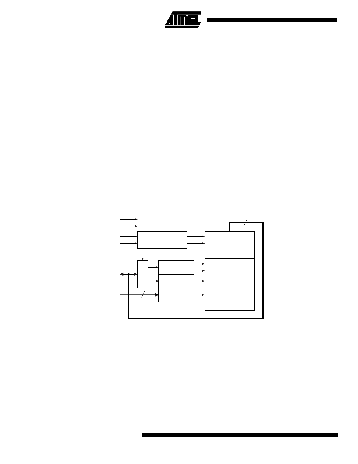
Block Diagram
programming equipment to select the proper programming
algorithms and voltages. The AT27LV520 programs exactly
the same way as a standard 5V AT27C520 and uses the
same programming equipment.
System Considerations
Switching under active conditions may produce transient
voltage excursions. Unless accommodated by the system
design, these transients may exceed data sheet limits,
resulting in device non-conformance. At a minimum, a
0.1 µF high frequency, low inherent inductance, ceramic
capacitor should be utilized for each device. This capacitor
should be connected between the V
nals of the device, as close to the device as possible. Additionally, to stabilize the supply voltage level on printed
circuit boards with large EPROM arrays, a 4.7 µF bulk electrolytic capacitor should be utilized, again connected
between the V
and Ground terminals. This capacitor
CC
should be positioned as close as possible to the point
where the power supply is connected to the array.
and Ground termi-
CC
VCC
GND
OE/VPP
ALE
AD7 - AD0
A15 - A8
OE, ALE, AND
PROGRAM LOGIC
Y DECODER
LATCHES
8
X DECODER
8
OUTPUT
BUFFERS
Y-GATING
CELL MATRIX
IDENTIFICATION
2
AT27LV520
Page 3
Absolute Maximum Ratings*
Temperature under Bias ................................ -55°C to +125°C
Storage Temperature ..................................... -65°C to +150°C
Voltage on Any Pin with
Respect to Ground .........................................-2.0V to +7.0V
Voltage on A9 with
Respect to Ground ......................................-2.0V to +14.0V
AT27LV520
*NOTICE: Stresses beyond those listed under “Absolute
Maximum Ratings” may cause permanent damage to the device. This is a stress rating only and
functional operation of the device at these or any
(1)
(1)
other conditions beyond those indicated in the
operational sections of this specification is not
implied. Exposure to absolute maximum rating
conditions for extended periods may affect device
reliability.
VPP Supply Voltage with
Respect to Ground .......................................-2.0V to +14.0V
(1)
Note: 1. Minimum voltage is -0.6V DC which may undershoot to -2.0V for pulses of less than 20 ns. Maximum output pin voltage is
+ 0.75V DC which may overshoot to +7.0V for pulses of less than 20 ns.
V
CC
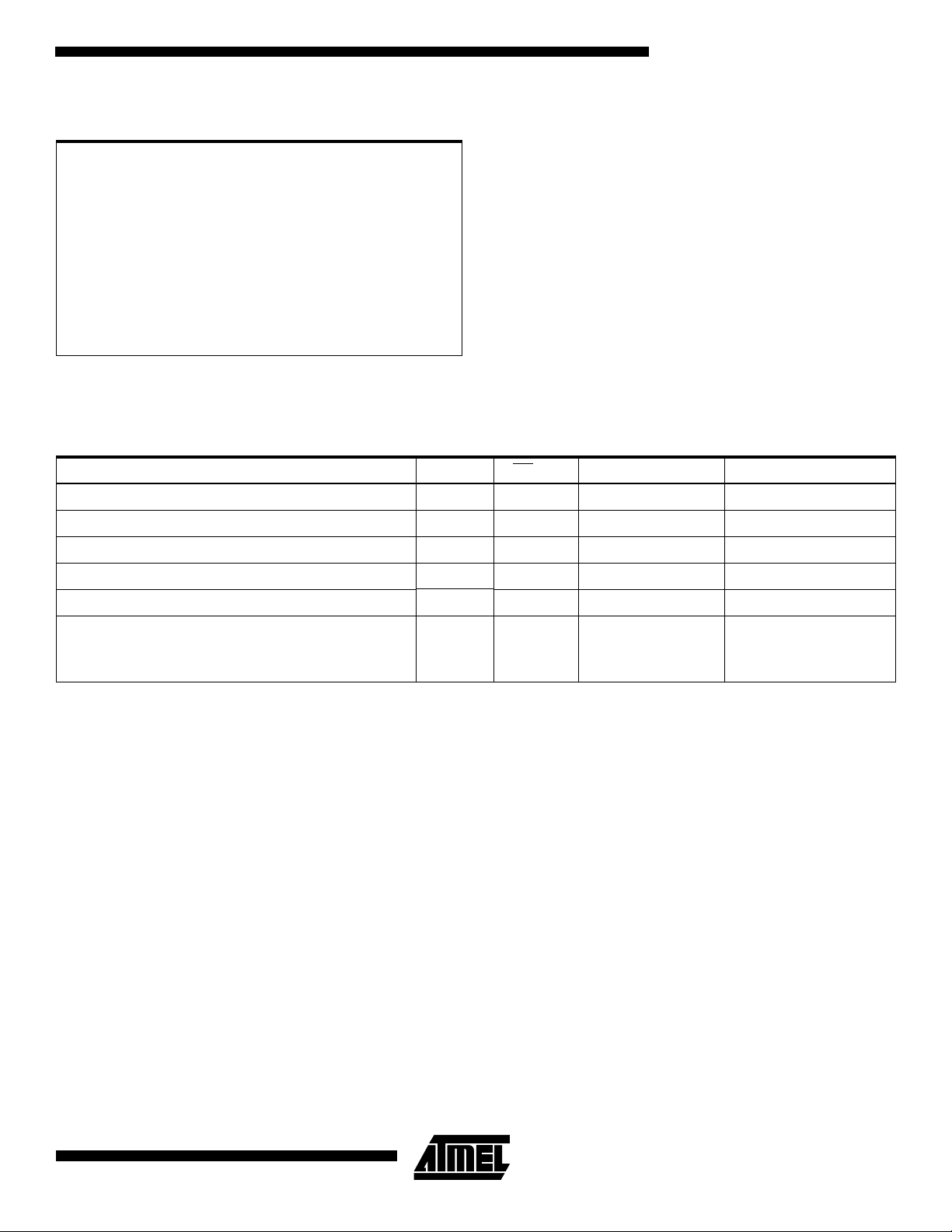
Operating Modes
Mode/Pin ALE OE/V
(2)
Read
Output Disable
(2)
Standby V
Address Latch Enable
Rapid Program
Product Identification
Notes: 1. X can be VIL or V
(2)
(3)
(4)
IH.
V
VIL/V
V
V
V
IL
IH
IH
IH
IH
IL
2. Read, output disable, and standby modes require 3.0V ≤ VCC ≤ 3.6V, or 4.5V ≤ VCC ≤ 5.5V.
3. Refer to Programming Characteristics.
= 12.0 ± 0.5V.
4. V
H
5. Two identifier bytes may be selected. All A8 - A15 inputs are held low (V
gled low (V
) to select the Manufacturer’s Identification byte and high (VIH) to select the Device Code byte.
IL
PP
V
IL
V
IH
V
IH
V
IH
V
PP
V
IL
IL
A8 - A15 AD0 - AD7
Ai D
(1)
X
OUT
High Z/A0 - A7
Ai A0 - A7
XA0 - A7
Ai D
A9 = V
A8 = VIH or V
A10 - A15 = V
(5)
H
IL
IL
Identification Code
IN
), except A9 which is set to VH and A8 which is tog-
3
Page 4
DC and AC Operating Conditions for Read Operation
AT27LV520-70 AT27LV520-90
Operating Temp. (Case)
Com. 0°C - 70°C0°C - 70°C
Ind. -40°C - +85°C-40°C - +85°C
Supply
V
CC
5V ±=10% 5V ±=10%
DC and Operating Characteristics for Read Operation
Symbol Parameter Condition Min Max Units
V
= 3.0V to 3.6V
CC
3.0V to 3.6V 3.0V to 3.6V
I
LI
I
LO
(1)
I
SB
I
CC
V
IL
V
IH
V
OL
V
OH
V
= 4.5V to 5.5V
CC
I
LI
I
LO
(1)
I
SB
I
CC
V
IL
V
IH
V
OL
V
OH
Note: 1. VCC standby current will be slightly higher with ALE, Ai, and ADi at TTL levels.
Input Load Current VIN = 0V to V
Output Leakage Current V
= 0V to V
OUT
CC
CC
±1µA
±5µA
VCC Standby Current ALE = VCC ± 0.3V; Ai, ADi = GND/VCC ± 0.3V 20 µA
VCC Active Current f = 5 MHz, I
= 0 mA, ALE = V
OUT
IL
8mA
Input Low Voltage -0.6 0.8 V
Input High Voltage 2.0 VCC + 0.5 V
Output Low Voltage IOL = 2.0 mA 0.4 V
Output High Voltage IOH = -2.0 mA 2.4 V
Input Load Current VIN = 0V to V
Output Leakage Current V
= 0V to V
OUT
CC
CC
±1µA
±5µA
VCC Standby Current ALE = VCC ± 0.3V; Ai, ADi = GND/VCC ± 0.3V 100 µA
VCC Active Current f = 5 MHz, I
= 0 mA, ALE = V
OUT
IL
20 mA
Input Low Voltage -0.6 0.8 V
Input High Voltage 2.0 VCC + 0.5 V
Output Low Voltage IOL = 2.1 mA 0.4 V
Output High Voltage IOH = -400 µA 2.4
4
AT27LV520
Page 5

AC Characteristics for Read Operation
VCC = 3.0V to 3.6V and 4.5V to 5.5V
Symbol Parameter Condition
(3)
t
ACC
t
CE
t
AS
t
AH
t
ALE
(3)
t
OE
(4)(5)
t
DF
t
OH
Note: 3, 4, 5 — see AC Waveforms for Read Operation
Address to Output Delay ALE = OE/VPP = V
Address Latch Enable Low to Output Delay Address Valid 55 70 ns
Address Setup Time OE/VPP = V
Address Hold Time OE/VPP = V
Address Latch Enable Width OE/VPP = V
OE/VPP to Output Delay ALE = V
OE/V
Output Hold from Address or OE/VPP,
High to Output Float ALE = V
PP
ALE = V
whichever occurred first
AT27LV520
AT27LV520-70 AT27LV520-90
UnitsMin Max Min Max
IL
IH
IH
IH
IL
IL
IL
12 15 ns
12 15 ns
40 45 ns
70ns
70 90 ns
30 35 ns
25 25 ns
AC Waveforms for Read Operation
(1)
tALE
ALE
tCE
PP
OE/V
tDF
tOH
DATA OUT
AD7 - AD0
tAS tAH
ADDRESS IN
tOE
tACC
A15 - A8
Notes: 1. Timing measurement reference levels for all speed grades are VOL = 0.8V and VOH = 2.0V. Input AC drive levels are VIL =
0.45V and V
/VPP may be delayed up to tCE - tOE after the address is valid without impact on tCE.
2. OE
/VPP may be delayed up to t
3. OE
= 2.4V.
IH
- tOE after the address is valid without impact on t
ACC
ACC
.
4. This parameter is only sampled and is not 100% tested.
5. Output float is defined as the point when data is no longer driven.
5
Page 6

Input Test Waveforms and
Output Test Load
Measurement Levels
tR, tF < 20 ns (10% to 90%)
Note: CL = 100 pF including jig capacitance.
Pin Capacitance
f = 1 MHz, T = 25°C
Symbol Typ Max Units Conditions
(1)
C
IN
C
OUT
Note: 1. Typical values for nominal supply voltage. This parameter is only sampled and is not 100% tested.
46pFV
812pFV
IN
OUT
= 0V
= 0V
6
AT27LV520
Page 7

Programming Waveforms
PROGRAM READ (VERIFY)
6.5V
VCC
5.0V
tVCS
13V
OE/VPP
V
IH
ALE
AD7 - AD0
A15 - A8
VIL
VIH
VIL
VIH
VIL
VIH
VIL
tLAS tLAH
tPRT
tLP
tALE
ADDR
tAS
Notes: 1. The Input Timing Reference is 0.8V for VIL and 2.0V for VIH.
2. t
OE
and t
are characteristics of the device but must be accommodated by the programmer.
DFP
tOES
tPW
DATA IN
tOEH
ADDRESS STABLE
AT27LV520
tVR
tALE
tDHtDS
ADDR
tLAHtLAS
tOE tDFP
DATA OUT
tAH
DC Programming Characteristics
TA = 25 ± 5°C, VCC = 6.5 ± 0.25V, OE/VPP = 13.0 ± 0.25V
Symbol Parameter Test Conditions
I
V
V
V
V
I
I
LI
IL
IH
OL
OH
CC2
PP2
Input Load Current VIN = VIL, V
IH
Input Low Level -0.6 0.8 V
Input High Level 2.0 V
Output Low Voltage I
= 2.1 mA 0.4 V
OL
Output High Voltage IOH = -400 µA 2.4 V
VCC Supply Current (Program and Verify) 25 mA
OE/VPP Current ALE = V
IH
Limits
±10 µA
+ 1.0 V
CC
25 mA
UnitsMin Max
7
Page 8

AC Programming Characteristics
TA = 25 ± 5°C, VCC = 6.5 ± 0.25V, OE/VPP = 13.0 ± 0.25V
Symbol Parameter
(1)
Test Conditions
Limits
UnitsMin Max
t
ALE
t
LAS
t
LAH
t
LP
t
OES
t
OEH
t
DS
t
DH
t
PW
t
VR
t
VCS
t
OE
t
DFP
t
AS
t
AH
t
PRT
Address Latch Enable Width
Latched Address Setup Time 100 ns
Latched Address Hold Time 100 ns
ALE Low to OE/VPP High Voltage Delay 2 µs
OE/VPP Setup Time 2 µs
OE/VPP Hold Time 2 µs
Data Setup Time 2 µs
Data Hold Time 2 µs
ALE Program Pulse Width
(2)
OE/VPP Recovery Time 2 µs
Input Rise and Fall Times:
(10% to 90%) 20 ns
Input Pulse Levels:
0.45V to 2.4V
Input Timing Reference Level:
0.8V to 2.0V
VCC Setup Time 2 µs
Data Valid from OE/V
PP
OE/VPP High to Output Float Delay
(3)
Output Timing Reference Level:
0.8V to 2.0V
Address Setup Time 2 µs
Address Hold Time 0 µs
OE/VPP Pulse Rise Time During
Programming
500 ns
47.5 52.5 µs
0 130 ns
50 ns
Notes: 1. VCC must be applied simultaneously or before OE/VPP and removed simultaneously or after OE/VPP.
2. Program Pulse width tolerance is 50=µsec=±=5%.
3. This parameter is only sampled and is not 100% tested. Output Float is defined as the point where data is no longer driven
— see timing diagram.
150 ns
Atmel’s 27LV520 Integrated Product Identification Code
Pins
Codes
Manufacturer 0000111101E
Device Type 1100111019D
Note: 1. The AT27LV520 has the same product identification code as the AT27C520. Both are programming compatible.
8
AT27LV520
Hex
DataA8 AD7 AD6 AD5 AD4 AD3 AD2 AD1 AD0
Page 9

™
Rapid
Programming Algorithm
A 50 µs ALE pulse width is used to program. The address
is set to the first location. V
is raised to 6.5V and OE/V
CC
PP
is raised to 13.0V. Each address is first programmed with
one 50 µs ALE pulse without verification. Then a verification/reprogramming loop is executed for each address. In
the event a byte fails to pass verification, up to 10 successive 50 µs pulses are applied with a verification after each
ADDR = FIRST LOCATION
VCC = 6.5V
VPP = 13.0V
PROGRAM ONE 50 µS PULSE
AT27LV520
pulse. If the byte fails to verify after 10 pulses have been
applied, the part is considered failed. After the byte verifies
properly, the next address is selected until all have been
checked. OE
bytes are read again and compared with the original data to
determine if the device passes or fails.
START
/VPP is then lowered to VIH and VCC to 5.0V. All
INCREMENT ADDRESS
INCREMENT ADDRESS
NO
LAST
ADDR.?
YES
NO
LAST
ADDR.?
YES
ADDR = FIRST LOCATION
X = 0
PASS
PROGRAM ONE 50 µS PULSE
VERIFY
BYTE
VCC = 5.0V
VPP = 5.0V
COMPARE
ALL BYTES
TO ORIGINAL
DATA
FAIL
FAIL
INCREMENT X
NO
X = 10?
YES
DEVICE
FAILED
PASS
PASSED
DEVICE
9
Page 10

Ordering Information
(mA)
I
CC
t
(ns)
ACC
90 8 AT27LV520-90SC
70 8 AT27LV520-70SC
Active Ordering Code Package Operation Range
AT27LV520-90XC
AT27LV520-90SI
AT27LV520-90XI
AT27LV520-70XC
AT27LV520-70SI
AT27LV520-70XI
20S
20X
20S
20X
20S
20X
20S
20X
Commercial
(0°C to 70°C)
Industrial
(-40°C to +85°C)
Commercial
(0°C to 70°C)
Industrial
(-40°C to +85°C)
Package Type
20S 20-lead, 0.300" Wide, Plastic Gull Wing Small Outline (SOIC)
20X 20-lead, 0.173" Wide, Thin Shrink Small Outline (TSSOP)
10
AT27LV520
Page 11

Packaging Information
AT27LV520
20S, 20-lead, 0.300" Wide,
Plastic Gull Wing Small Outline
Dimensions in Inches and (Millimeters)
0.020 (0.508)
0.013 (0.330)
0.299 (7.60)
PIN 1
0
8
REF
0.035 (0.889)
0.015 (0.381)
.050 (1.27) BSC
0.513 (13.0)
0.497 (12.6)
0.012 (0.305)
0.003 (0.076)
0.291 (7.39)
0.013 (0.330)
0.009 (0.229)
0.420 (10.7)
0.393 (9.98)
0.105 (2.67)
0.092 (2.34)
20X, 20-lead, 0.173" Wide,
Thin Super Small Outline Package (TSSOP)
Dimensions in (Millimeters) and Inches
0.30(0.012)
0.18(0.007)
PIN 1 ID
0
REF
8
6.60(.260)
6.40(.252)
0.70(.028)
0.50(.020)
4.48(.176)
4.30(.169)
0.65(.0256) BSC
0.15(.006)
0.05(.002)
6.50(.256)
6.25(.246)
1.10(0.043) MAX
0.18(.007)
0.09(.003)
11
Page 12

Atmel Headquarters Atmel Operations
Corporate Headquarters
2325 Orchard Parkway
San Jose, CA 95131
TEL (408) 441-0311
FAX (408) 487-2600
Europe
Atmel U.K., Ltd.
Coliseum Business Centre
Riverside Way
Camberley, Surrey GU15 3YL
England
TEL (44) 1276-686-677
FAX (44) 1276-686-697
Asia
Atmel Asia, Ltd.
Room 1219
Chinachem Golden Plaza
77 Mody Road Tsimhatsui
East Kowloon
Hong Kong
TEL (852) 2721-9778
FAX (852) 2722-1369
Japan
Atmel Japan K.K.
9F, Tonetsu Shinkawa Bldg.
1-24-8 Shinkawa
Chuo-ku, Tokyo 104-0033
Japan
TEL (81) 3-3523-3551
FAX (81) 3-3523-7581
Atmel Colorado Springs
1150 E. Cheyenne Mtn. Blvd.
Colorado Springs, CO 80906
TEL (719) 576-3300
FAX (719) 540-1759
Atmel Rousset
Zone Industrielle
13106 Rousset Cedex
France
TEL (33) 4-4253-6000
FAX (33) 4-4253-6001
Fax-on-Demand
North America:
1-(800) 292-8635
International:
1-(408) 441-0732
e-mail
literature@atmel.com
Web Site
http://www.atmel.com
BBS
1-(408) 436-4309
© Atmel Corporation 2000.
Atmel Corporation makes no warranty for the use of its products, other than those expressly contained in the Company’s standard warranty which is detailed in Atmel’s Terms and Conditions located on the Company’s web site. The Company assumes no responsibility for
any errors which may appear in this document, reserves the right to change devices or specifications detailed herein at any time without
notice, and does not make any commitment to update the information contained herein. No licenses to patents or other intellectual property of Atmel are granted by the Company in connection with the sale of Atmel products, expressly or by implication. Atmel’s products are
not authorized for use as critical components in life support devices or systems.
Marks bearing ® and/or ™ are registered trademarks and trademarks of Atmel Corporation.
Terms and product names in this document may be trademarks of others.
Printed on recycled paper.
0911D–05/00/xM
 Loading...