

Page 1
Features
• Fast Read Access Time - 90 ns
• Dual Voltage Range Operation
– Low Voltage Power Supply Range, 3.0V to 3.6V
– or Standard 5V ± 10% Supply Range
• Compatible with JEDEC Standard AT27C020
• Low Power CMOS Operation
– 20 µA max. (less than 1 µA typical) Standby for V
– 29 mW max. Active at 5 MHz for VCC = 3.6V
= 3.6V
CC
• JEDEC Standard Packages
– 32-lead PLCC
– 32-lead TSOP (8 x 20 mm)
– 32-lead VSOP (8 x 14 mm)
• High Reliability CMOS Technology
– 2,000V ESD Protection
– 200 mA Latchup Immunity
• Rapid™ Programming Algorithm - 100 µs/byte (typical)
• Two-line Control
• CMOS and TTL Compatible Inputs and Outputs
– JEDEC Standard for LVTTL
• Integrated Product Identification Code
• Commercial and Industrial Temperature Ranges
Description
The AT27LV020A is a high performance, low power, low voltage 2,097,152 bit onetime programmable read only memory (OTP EPROM) organized as 256K by 8 bits. It
requires only one supply in the range of 3.0 to 3.6V in normal read mode operation,
making it ideal for fast, portable systems using battery power.
2-Megabit
(256K x 8)
Low Voltage
OTP EPROM
AT27LV020A
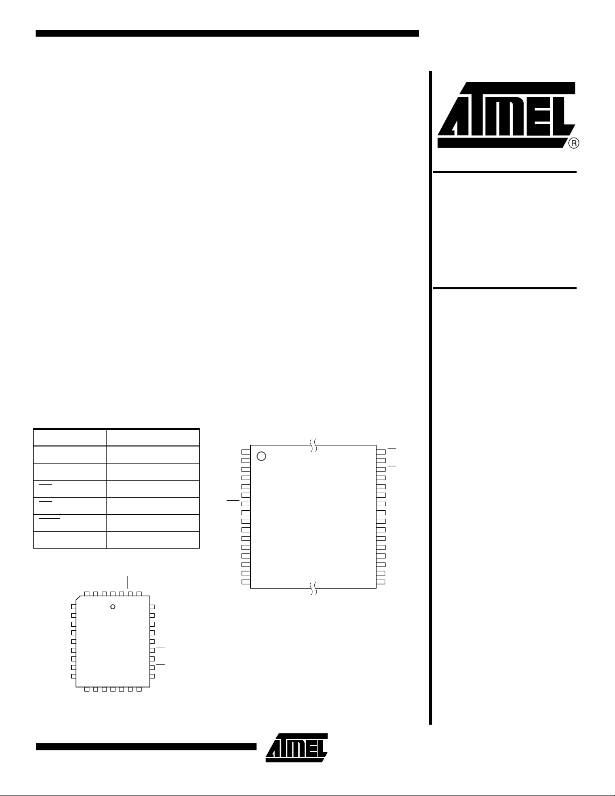
Pin Configurations
Pin Name Function
A0 - A17 Addresses
O0 - O7 Outputs
CE
OE
PGM
NC No Connect
PLCC, Top View
5
A7
6
A6
7
A5
8
A4
9
A3
10
A2
11
A1
12
A0
13
O0
Chip Enable
Output Enable
Program Strobe
A12
A15
A16
VPP
VCC
PGM
432
1
323130
14151617181920
O1
O2
O3O4O5
GND
A17
29
28
27
26
25
24
23
22
21
O6
A14
A13
A8
A9
A11
OE
A10
CE
O7
A11
A13
A14
A17
PGM
VCC
VPP
A16
A15
A12
(continued)
TSOP/VSOP Top View
Typ e 1
1
2
A9
3
A8
4
5
6
7
8
9
10
11
12
13
A7
14
A6
15
A5
16
A4
OE
32
A10
31
CE
30
O7
29
O6
28
O5
27
O4
26
O3
25
GND
24
02
23
01
22
O0
21
A0
20
A1
19
A2
18
A3
17
Rev. 0549E–04/01
1
Page 2
Atmel’s innovative design techniques provide fast speeds
that rival 5V parts while keeping the low power consumption of a 3V supply. At V
= 3.0V, any byte can be
CC
accessed in less than 90 ns. With a typical power dissipation of only 18 mW at 5 MHz and V
= 3.3V, the
CC
AT27LV020A consumes less than one fifth the power of a
standard 5V EPROM. Standby mode supply current is typically less than 1 µA at 3.3V.
The AT27LV020A is available in industry standard JEDEC
approved one-time programmable (OTP) plastic PLCC,
TSOP, and VSOP. All devices feature two-line control (CE
) to give designers the flexibility to prevent bus
OE
contention.
The AT27LV020A operating with V
at 3.0V produces TTL
CC
level outputs that are compatible with standard TTL logic
devices operating at V
= 5.0V. The device is also capa-
CC
ble of standard 5-volt operation making it ideally suited for
dual supply range systems or card products that are pluggable in both 3-volt and 5-volt hosts.
Atmel's AT27LV020A has additional features to ensure
high quality and efficient production use. The Rapid
™
Programming Algorithm reduces the time required to program
the part and guarantees reliable programming. Programming time is typically only 100 µs/byte. The Integrated
Product Identification Code electronically identifies the
device and manufacturer. This feature is used by industry
standard programming equipment to select the proper programming algorithms and voltages. The AT27LV020A programs exactly the same way as a standard 5V AT27C020
and uses the same programming equipment.
System Considerations
Switching between active and standby conditions via the
Chip Enable pin may produce transient voltage excursions.
,
Unless accommodated by the system design, these transients may exceed data sheet limits, resulting in device
non-conformance. At a minimum, a 0.1 µF high frequency,
low inherent inductance, ceramic capacitor should be utilized for each device. This capacitor should be connected
between the V
close to the device as possible. Additionally, to stabilize the
supply voltage level on printed circuit boards with large
EPROM arrays, a 4.7 µF bulk electrolytic capacitor should
be utilized, again connected between the V
terminals. This capacitor should be positioned as close as
possible to the point where the power supply is connected
to the array.
and Ground terminals of the device, as
CC
and Ground
CC
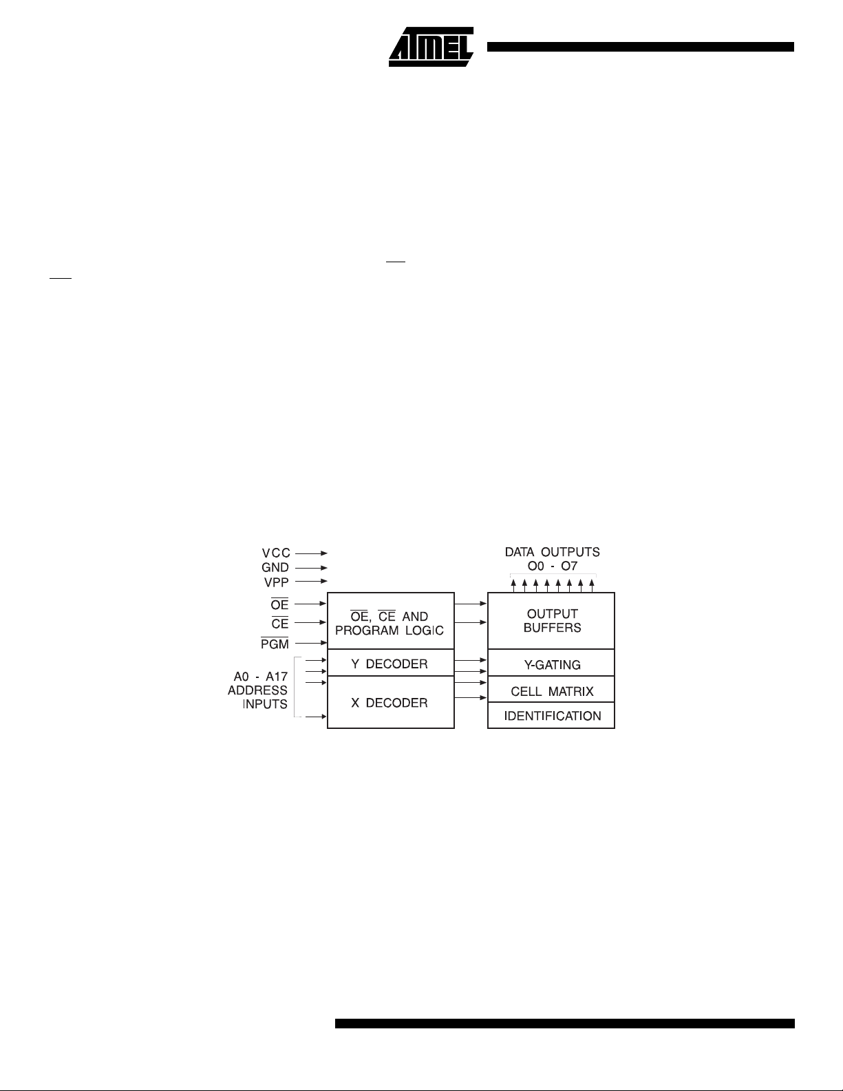
Block Diagram
2
AT27LV020A
Page 3
Absolute Maximum Ratings*
Temperature Under Bias.................................. -40°C to +85°C
Storage Temperature..................................... -65°C to +125°C
Voltage on any Pin with
with Respect to Ground..................................-2.0V to +7.0V
Voltage on A9 with
Respect to Ground .......................................-2.0V to +14.0V
AT27LV020A
*NOTICE: Stresses beyond those listed under “Absolute
Maximum Ratings” may cause permanent damage to the device. This is a stress rating only and
functional operation of the device at these or any
(1)
(1)
other conditions beyond those indicated in the
operational sections of this specification is not
implied. Exposure to absolute maximum rating
conditions for extended periods may affect device
reliability.
VPP Supply Voltage with
Respect to Ground .......................................-2.0V to +14.0V
(1)
Note: 1. Minimum voltage is -0.6V DC which may undershoot to -2.0V for pulses of less than 20 ns. Maximum output pin voltage is
VCC + 0.75V DC which may be exceeded if certain precautions are observed (consult application notes) and which may
overshoot to +7.0V for pulses of less than 20 ns.
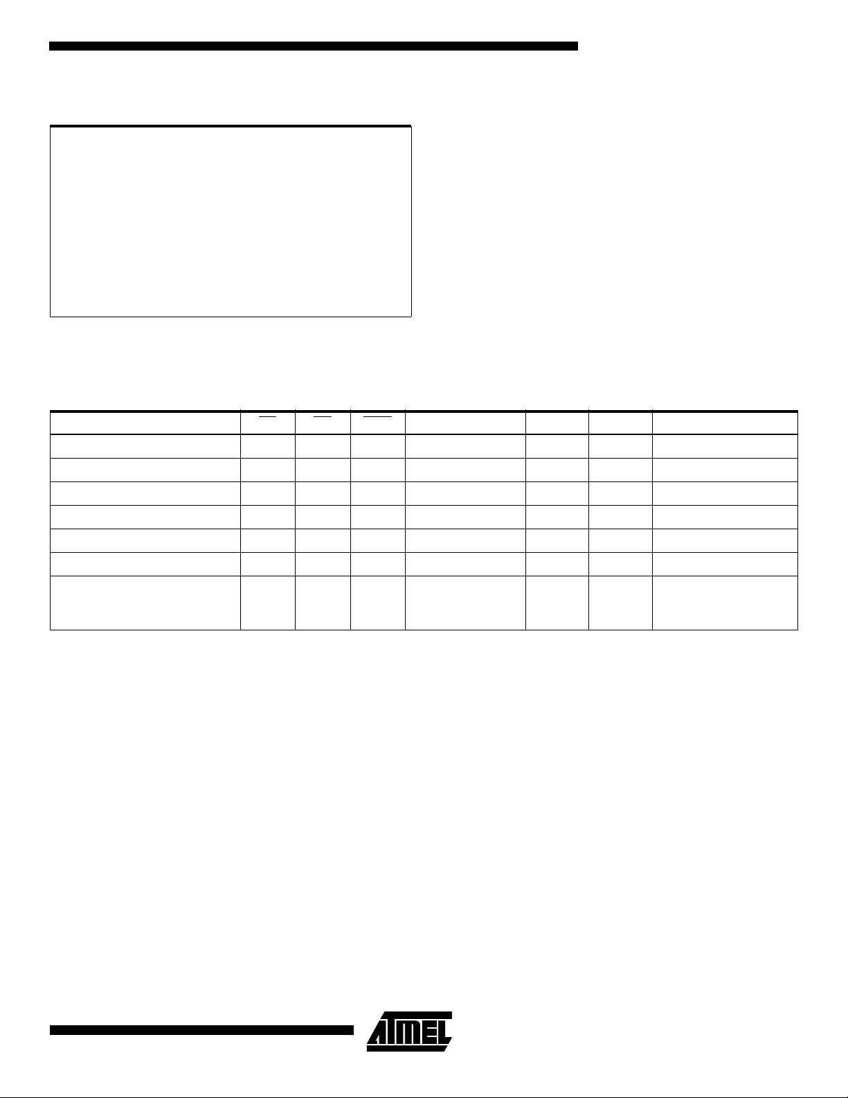
Operating Modes
Mode/Pin CE OE PGM Ai V
(2)
Read
Output Disable
Standby
Rapid Program
PGM Verify
PGM Inhibit
(2)
(2)
(3)
(3)
(3)
Product Identification
(3)(5)
V
IL
V
IL
XVIHXX XV
V
IH
V
IL
V
IL
V
IH
V
IL
XX X XV
V
IH
V
IL
XX X VPPV
V
IL
(1)
X
V
IL
V
IH
X
Ai X V
Ai V
Ai V
A9 = V
A0 = VIH or V
A1 - A17 = V
(4)
H
IL
IL
Notes: 1. X can be VIL or VIH.
2. Read, output disable, and standby modes require, 3.0V ≤ V
3. Refer to Programming Characteristics. Programming modes require V
≤=3.6V, or 4.5V ≤ VCC ≤ 5.5V.
CC
= 6.5V.
CC
4. VH = 12.0 ± 0.5V.
5. Two identifier bytes may be selected. All Ai inputs are held low (V
low (V
) to select the Manufacturer’s Identification byte and high (VIH) to select the Device Code byte.
IL
), except A9 which is set to VH and A0 which is toggled
IL
PP
PP
PP
XV
V
CC
CC
CC
CC
V
CC
V
CC
CC
CC
Outputs
(2)
D
OUT
(2)
High Z
(2)
High Z
(3)
D
IN
(3)
D
OUT
(3)
High Z
(3)
Identification Code
3
Page 4
DC and AC Operating Conditions for Read Operation
AT27LV020A-90 AT27LV020A-12 AT27LV020A-15
Operating Temperature
(Case)
Com. 0°C - 70°C0°C - 70°C0°C - 70°C
Ind. -40°C - 85°C-40°C - 85°C-40°C - 85°C
Power Supply
V
CC
5V ± 10% 5V ± 10% 5V ± 10%
DC and Operating Characteristics for Read Operation
Symbol Parameter Condition Min Max Units
V
= 3.0V to 3.6V
CC
3.0V to 3.6V 3.0V to 3.6V 3.0V to 3.6V
I
LI
I
LO
(2)
I
PP1
I
SB
I
CC
V
IL
V
IH
V
OL
V
OH
V
= 4.5V to 5.5V
CC
I
LI
I
LO
(2)
I
PP1
I
SB
I
CC
V
IL
V
IH
V
OL
V
OH
Notes: 1. VCC must be applied simultaneously with or before VPP, and removed simultaneously with or after VPP.
Input Load Current VIN = 0V to V
Output Leakage Current V
Read/Standby Current
VCC Standby Current
(1)
(1)
= 0V to V
OUT
VPP = V
I
I
CC
(CMOS), CE = V
SB1
(TTL), CE = 2.0 to VCC + 0.5V 100 µA
SB2
VCC Active Current f = 5 MHz, I
CC
CC
CC=
= 0 mA, CE = V
OUT
± 0.3V 20 µA
IL
±1µA
±5µA
10 µA
8mA
Input Low Voltage -0.6 0.8 V
Input High Voltage 2.0 VCC + 0.5 V
Output Low Voltage IOL = 2.0 mA 0.4 V
Output High Voltage IOH = -2.0=mA 2.4 V
Input Load Current VIN = 0V to V
Output Leakage Current V
Read/Standby Current
VCC Standby Current
(1)
(1)
= 0V to V
OUT
VPP = V
I
I
CC
(CMOS), CE = VCC ± 0.3V 100 µA
SB1
(TTL), CE = 2.0 to VCC + 0.5V 1 mA
SB2
VCC Active Current f = 5 MHz, I
CC
CC
= 0 mA, CE = V
OUT
IL
±1µA
±5µA
10 µA
25 mA
Input Low Voltage -0.6 0.8 V
Input High Voltage 2.0 VCC + 0.5 V
Output Low Voltage IOL = 2.1 mA 0.4 V
Output High Voltage IOH = -400 µA 2.4 V
may be connected directly to VCC, except during programming. The supply current would then be the sun of ICC and IPP.
2. V
PP
4
AT27LV020A
Page 5

AC Characteristics for Read Operation
VCC = 3.0V to 3.6V and 4.5V to 5.5V
AT27LV020A
AT27LV020A
-90 -12 -15
Symbol Parameter Condition
(3)
t
t
t
t
ACC
CE
OE
DF
(2)
(2)(3)
(4)(5)
Address to Output Delay CE = OE = V
CE to Output Delay OE = V
OE to Output Delay CE = V
OE or CE High to Output Float,
whichever occurred first
t
OH
Output Hold from Address, CE or OE,
whichever occurred first
AC Waveforms for Read Operation
Min Max Min Max Min Max
IL
IL
IL
90 120 150 ns
90 120 150 ns
50 50 60 ns
Units
40 40 50 ns
000ns
Notes: 1. Timing measurement references are 0.8V and 2.0V. Input AC drive levels are 0.45V and 2.4V, unless otherwise specified.
2. OE may be delayed up to tCE - tOE after the falling edge of CE without impact on tCE.
3. OE
may be delayed up to t
- tOE after the address is valid without impact on t
ACC
ACC
.
4. This parameter is only sampled and is not 100% tested.
5. Output float is defined as the point when data is no longer driven.
5
Page 6

Input Test Waveform and
Output Test Load
Measurement Level
tR, tF < 20 ns (1% to 90%)
Note: CL = 1 pF including jig capacitance.
Pin Capacitance
f = 1 MHz, T = 25°C
Symbol Typ Max Units Conditions
(1)
C
IN
C
OUT
Note: 1. Typical values for nominal supply voltage. This parameter is only sampled and is not 100% tested.
48pFV
812pFV
IN
OUT
= 0V
= 0V
6
AT27LV020A
Page 7

AT27LV020A
Programming Waveforms
(1)
Notes: 1. The Input Timing Reference is 0.8V for VIL and 2.0V for VIH.
2. tOE and t
are characteristics of the device but must be accommodated by the programmer.
DFP
3. When programming the AT27LV020A a 0.1 µF capacitor is required across V
transients.
DC Programming Characteristics
TA = 25 ± 5°C, VCC = 6.5 ± 0.25V, VPP = 13.0 ± 0.25V
Symbol Parameter Test Conditions
I
V
V
V
V
I
I
V
LI
IL
IH
OL
OH
CC2
PP2
ID
Input Load Current V
= VIL, V
IN
IH
Input Low Level -0.6 0.8 V
Input High Level 2.0 VCC + 0.5 V
Output Low Voltage IOL = 2.1 mA 0.4 V
Output High Voltage IOH = -400=µA 2.4 V
VCC Supply Current (Program and Verify) 40 mA
VPP Supply Current CE = PGM = V
A9 Product Identification Voltage 11.5 12.5 V
and ground to suppress spurious voltage
PP
Limits
UnitsMin Max
±10 µA
IL
20 mA
7
Page 8

AC Programming Characteristics
TA = 25 ± 5°C, VCC = 6.5 ± 0.25V, VPP = 13.0 ± 0.25V
Symbol Parameter Test Conditions
Limits
(1)
UnitsMin Max
t
AS
t
CES
t
OES
t
DS
t
AH
t
DH
t
DFP
t
VPS
t
VCS
t
PW
t
OE
t
PRT
Address Setup Time
CE Setup Time 2 µs
OE Setup Time 2 µs
Data Setup Time 2 µs
Address Hold Time 0 µs
Data Hold Time 2 µs
OE High to Output Float Delay
(3)
VPP Setup Time 2 µs
Input Rise and Fall Times
(10% to 90%) 20 ns
Input Pulse Levels
0.45V to 2.4V
Input Timing Reference Level
0.8V to 2.0V
VCC Setup Time 2 µs
PGM Program Pulse Width
(2)
Data Valid from OE 150 ns
Output Timing Reference Level
0.8V to 2.0V
VPP Pulse Rise Time During
Programming
2µs
0 130 ns
95 105 µs
50 ns
Notes: 1. VCC must be applied simultaneously or before VPP and removed simultaneously or after VPP.
2. This parameter is only sampled and is not 100% tested. Output Float is defined as the point where data is no longer driven
—see timing diagram.
3. Program Pulse width tolerance is 100 µsec=±=5%.
Atmel’s 27LV020A Integrated Product Identification Code
(1)
Pins
Codes
Hex
DataA0 O7 O6 O5 O4 O3 O2 O1 O0
Manufacturer 0 00011110 1E
Device Type 1 10000110 86
Note: 1. The AT27LV020A has the same Product Identification Code as the AT27C020. Both are programming compatible.
8
AT27LV020A
Page 9

Rapid Programming Algorithm
A 100 µs PGM pulse width is used to program. The
address is set to the first location. V
is raised to 13.0V. Each address is first programmed
V
PP
with one 100 µs PGM
verification/reprogramming loop is executed for each
address. In the event a byte fails to pass verification, up to
10 successive 100 µs pulses are applied with a verification
pulse without verification. Then a
is raised to 6.5V and
CC
AT27LV020A
after each pulse. If the byte fails to verify after 10 pulses
have been applied, the part is considered failed. After the
byte verifies properly, the next address is selected until all
have been checked. V
5.0V. All bytes are read again and compared with the original data to determine if the device passes or fails.
is then lowered to 5.0V and V
PP
CC
to
9
Page 10

Ordering Information
ICC (mA)
V
= 3.6V
t
ACC
(ns)
90 8 0.02 AT27LV020A-90JC
120 8 0.02 AT27LV020A-12JC
150 8 0.02 AT27LV020A-15JC
CC
Ordering Code Package Operation RangeActive Standby
AT27LV020A-90TC
AT27LV020A-90VC
8 0.02 AT27LV020A-90JI
AT27LV020A-90TI
AT27LV020A-90VI
AT27LV020A-12TC
AT27LV020A-12VC
8 0.02 AT27LV020A-12JI
AT27LV020A-12TI
AT27LV020A-12VI
AT27LV020A-15TC
AT27LV020A-15VC
8 0.02 AT27LV020A-15JI
AT27LV020A-15TI
AT27LV020A-15VI
32J
32T
32V
32J
32T
32V
32J
32T
32V
32J
32T
32V
32J
32T
32V
32J
32T
32V
Commercial
(0°C to 70°C)
Industrial
(-40°C to 85°C)
Commercial
(0°C to 70°C)
Industrial
(-40°C to 85°C)
Commercial
(0°C to 70°C)
Industrial
(-40°C to 85°C)
Package Type
32J 32-Lead, Plastic J-Leaded Chip Carrier (PLCC)
32T 32-Lead, Plastic Thin Small Outline Package (TSOP) 8 x 20 mm
32V 32-Lead, Plastic Thin Small Outline Package (VSOP) 8 x 14 mm
10
AT27LV020A
Page 11

Packaging Information
AT27LV020A
32J, 32-Lead, Plastic J-Leaded Chip Carrier (PLCC)
Dimensions in Inches and (Millimeters)
JEDEC STANDARD MS-016 AE
.045(1.14) X 45˚
.032(.813)
.026(.660)
.050(1.27) TYP
PIN NO. 1
IDENTIFY
.553(14.0)
.547(13.9)
.300(7.62) REF
.430(10.9)
.390(9.90)
AT CONTACT
POINTS
.453(11.5)
.447(11.4)
.495(12.6)
.485(12.3)
.025(.635) X 30˚ - 45˚
.595(15.1)
.585(14.9)
.021(.533)
.013(.330)
.140(3.56)
.120(3.05)
.022(.559) X 45˚ MAX (3X)
.012(.305)
.008(.203)
.030(.762)
.015(.381)
.095(2.41)
.060(1.52)
.530(13.5)
.490(12.4)
32T, 32-Lead, Plastic Thin Small Outline Package
(TSOP)
Dimensions in Millimeters and (Inches)*
JEDEC OUTLINE MO-142 BD
INDEX
MARK
0.50(.020)
BSC
0
REF
5
7.50(.295)
REF
8.20(.323)
7.80(.307)
0.15(.006)
0.05(.002)
18.5(.728)
18.3(.720)
0.25(.010)
0.15(.006)
0.70(.028)
0.50(.020)
20.2(.795)
19.8(.780)
1.20(.047) MAX
0.20(.008)
0.10(.004)
*Controlling dimensions: millimeters
32V, 32-Lead, Plastic Thin Small Outline Package
(VSOP)
Dimensions in Inches and (Millimeters)
JEDEC OUTLINE MO-142 BA
INDEX
MARK
0.50(.020)
BSC
0
REF
5
7.50(.295)
REF
8.10(.319)
7.90(.311)
0.15(.006)
0.05(.002)
12.5(.492)
12.3(.484)
0.25(.010)
0.15(.006)
0.70(.028)
0.50(.020)
14.2(.559)
13.8(.543)
1.20(.047) MAX
0.20(.008)
0.10(.004)
11
Page 12

Atmel Headquarters Atmel Operations
Corporate Headquarters
2325 Orchard Parkway
San Jose, CA 95131
TEL (408) 441-0311
FAX (408) 487-2600
Europe
Atmel SarL
Route des Arsenaux 41
Casa Postale 80
CH-1705 Fribourg
Switzerland
TEL (41) 26-426-5555
FAX (41) 26-426-5500
Asia
Atmel Asia, Ltd.
Room 1219
Chinachem Golden Plaza
77 Mody Road Tsimhatsui
East Kowloon
Hong Kong
TEL (852) 2721-9778
FAX (852) 2722-1369
Japan
Atmel Japan K.K.
9F, Tonetsu Shinkawa Bldg.
1-24-8 Shinkawa
Chuo-ku, Tokyo 104-0033
Japan
TEL (81) 3-3523-3551
FAX (81) 3-3523-7581
Atmel Colorado Springs
1150 E. Cheyenne Mtn. Blvd.
Colorado Springs, CO 80906
TEL (719) 576-3300
FAX (719) 540-1759
Atmel Rousset
Zone Industrielle
13106 Rousset Cedex
France
TEL (33) 4-4253-6000
FAX (33) 4-4253-6001
Atmel Smart Card ICs
Scottish Enterprise Technology Park
East Kilbride, Scotland G75 0QR
TEL (44) 1355-357-000
FAX (44) 1355-242-743
Atmel Grenoble
Avenue de Rochepleine
BP 123
38521 Saint-Egreve Cedex
France
TEL (33) 4-7658-3000
FAX (33) 4-7658-3480
Fax-on-Demand
North America:
e-mail
literature@atmel.com
1-(800) 292-8635
International:
1-(408) 441-0732
Web Site
http://www.atmel.com
BBS
1-(408) 436-4309
© Atmel Corporation 2001.
Atmel Corporation makes no warranty for the use of its products, other than those expressly contained in the Company’s standard warranty which is detailed in Atmel’s Terms and Conditions located on the Company’s website. The Company assumes no responsibility for
any errors which may appear in this document, reserves the right to change devices or specifications detailed herein at any time without
notice, and does not make any commitment to update the information contained herein. No licenses to patents or other intellectual property of Atmel are granted by the Company in connection with the sale of Atmel products, expressly or by implication. Atmel’s products are
not authorized for use as critical components in life support devices or systems.
Marks bearing ® and/or ™ are registered trademarks and trademarks of Atmel Corporation.
Terms and product names in this document may be trademarks of others
Printed on recycled paper.
0549E–04/01/xM
 Loading...