

Page 1
Features
•
Read Access Time - 90 ns
•
Word-wide or Byte-wide Configurable
•
8-Megabit Flash and Mask ROM Compatable
•
Low Power CMOS Operation
–100 µA Maximum Standby
– 50 mA Maximum Active at 5 MHz
•
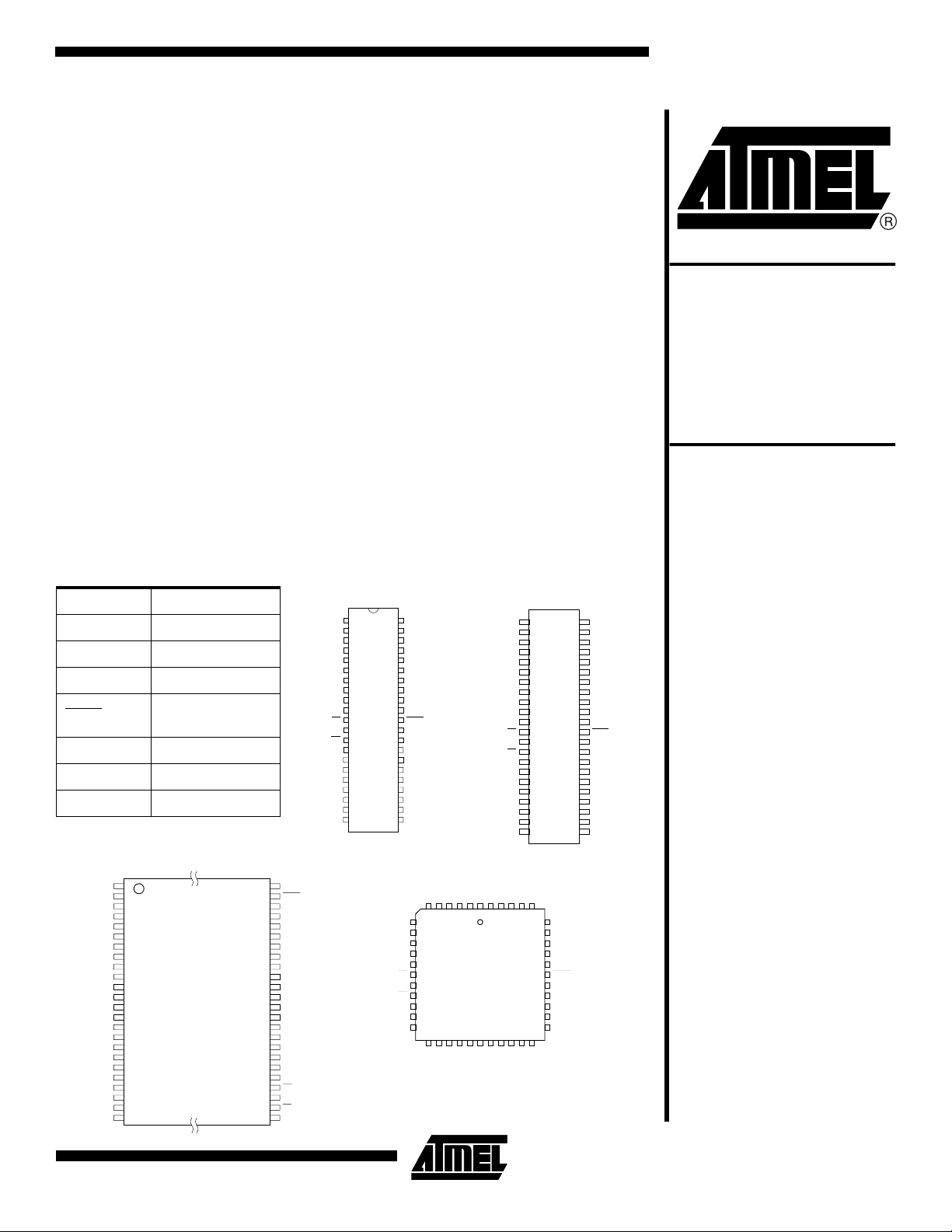
Wide Selection of JEDEC Standard Packages
– 42-Lead 600 mil PDIP
– 44-Lead PLCC
– 44-Lead SOIC (SOP)
– 48-Lead TSOP (12 mm x 20 mm)
±±±±
•
5V
10% Power Supply
•
High Reliability CMOS Technology
– 2,000 ESD Protection
– 200 mA Latchup Immunity
•
Rapid™ Programming Algorithm - 50 µs/word (typical)
•
CMOS and TTL Compatible Inputs and Outputs
•
Integrated Product Identification Code
•
Commercial and Industrial Temperature Ranges
8-Megabit
(512K x 16 or
1024K x 8)
OTP EPROM
Description
The AT27C800 is a low-power, high performance 8,388,608-bit UV erasable programmable read only memory (EPROM) organized as either 512K by 16 or 1024K by 8
(continued)
Pin Configurations
Pin Name Function
A0 - A18 Addresses
O0 - O15 Outputs
O15/A-1 Output/Address
BYTE
/VPP
Byte Mode/
Program Supp ly
CE Chip Enable
OE Output Enable
NC No Connect
TSOP
Type 1
1
A15
2
A14
3
A13
4
A12
5
A11
6
A10
7
A9
8
A8
9
NC
10
NC
11
NC
12
NC
13
NC
14
NC
15
NC
16
A18
17
A17
18
A7
19
A6
20
A5
21
A4
22
A3
23
A2
24
A1
PDIP Top View
1
A18
A17
A7
A6
A5
A4
A3
A2
A1
A0
CE
GND
OE
O0
O8
O1
O9
O2
O10
O3
O11
48
A16
47
BYTE/VPP
46
GND
45
O15/A-1
44
O7
43
O14
42
O6
41
O13
40
O5
39
O12
38
O4
37
VCC
36
O11
35
O3
34
O10
33
O2
32
O9
31
O1
30
O8
29
O0
28
OE
27
GND
26
CE
25
A0
42
41
40
39
38
37
36
35
34
33
32
31
30
29
28
27
26
25
24
23
22
NC
A8
A9
A10
A11
A12
A13
A14
A15
A16
BYTE/VPP
GND
O15/A-1
O7
O14
O6
O13
O5
O12
O4
VCC
2
3
4
5
6
7
8
9
10
11
12
13
14
15
16
17
18
19
20
21
PLCC Top View
A5A6A7
A17
65432
7
A4
8
A3
9
A2
10
A1
11
A0
12
CE
13
GND
14
OE
15
O0
16
O8
17
O1
1819202122232425262728
O9
O2
O10O3O11
Note: PLCC Package Pin 23 is
DON’T CONNECT.
NC
A18
A17
A7
A6
A5
A4
A3
A2
A1
A0
CE
GND
OE
O0
O8
O1
O9
O2
O10
O3
O11
A18NCNCA8A9
1
4443424140
O4
NC
VCC
SOIC (SOP)
1
44
2
43
3
42
4
41
5
40
6
39
7
38
8
37
9
36
10
35
11
34
12
33
13
32
14
31
15
30
16
29
17
28
18
27
19
26
20
25
21
24
22
23
A10
A11
39
A12
38
A13
37
A14
36
A15
35
A16
34
BYTE/VPP
33
GND
32
O15/A-1
31
O7
30
O14
29
O6
O12O5O13
NC
NC
A8
A9
A10
A11
A12
A13
A14
A15
A16
BYTE/VPP
GND
O15/A-1
O7
O14
O6
O13
O5
O12
O4
VCC
AT27C800
Rev. 0801B–10/98
1
Page 2
bits. It requires a single 5V power supply in normal read
mode operation. Any word can be accessed in less than 90
ns, eliminating th e need for speed -reducing WAIT states .
The x16 organ ization makes th is par t ideal for high -perfor mance 16- and 32-bit microprocessor systems.
The AT27C800 can be organized as either word-wide or
byte-wide. The org anizatio n is se lected v ia the B YTE
/V
PP
pin. When BYTE/VPP is asserted high (VIH), the word-wide
organization is sele cted and the O15/A-1 pi n is used for
O15 data output. When BYTE
/VPP is asserted low (VIL),the
byte wide organization is se lected and the O 15/A-1 pin is
used for the address pin A-1. When the AT27C800 is logically regarded as x16 (word-wide), but read in the bytewide mode, then with A-1=V
bit word are selected with A-1 =V
the lower eight bits of the 16
IL
the upper 8 bits of the
IH
16-bit word are selected.
In read mode, the AT27C800 typically consumes 15 mA.
Standby mode supply current is typically less than 10 µA.
The AT27C800 is available in industry standard JEDEC-
approved one -time prog rammable ( OTP) PLCC , PDIP,
SOIC (SOP), and TSOP a s well as UV er asab le win dowed
Cerdip packages. The device features two-line control(CE
,OE) to eliminate bus contention in high-speed sys-
tems.
With high den sity 51 2K word o r 1 024K -bit stor age capa bil-
ity, the AT27C800 allows firmware to be to be stored reliably and to be accessed by the system without the delays
of mass storage media.
Atmel’s AT27C800 has additional features that ensure high
quality and effic ient p roducti on us e. The Rapid
TM
Programming Algorithm reduces the time required to program the
part and guarantees reliable programming. Programming
time is typically only 50µs/word. The Integrated Prod uct
Identification Code electronically ide ntifies the device and
manufacturer. This feature is used by industry standard
programming eq uipme nt to sele ct the prop er program ming
equipment and voltages.
System Considerations
Switching between active and standby conditions via the
Chip Enable pin may produce transient voltage excursions.
Unless accommodated by the system design, these transients may exceed data sheet limits, resulting in device
non-conforman ce. At a mini mum, a 0.1 µF high frequency,
low inherent inductance, ceramic capacitor should be utilized for each device. This capacitor should be connected
between the V
close to the device as possible. Additionally, to stabilize the
supply voltage level on printed circuit boards with large
EPROM arrays, a 4.7 µF bulk electrolytic capacitor should
be utilized, again connected between the V
terminals. This capacitor should be positioned as close as
possible to the point where the power supply is connected
to the array.
and Ground terminals of the device, as
CC
and Ground
CC
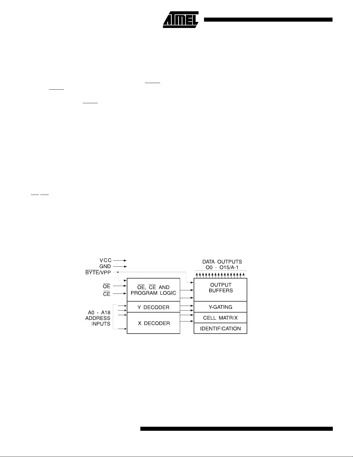
Block Diagram
2
AT27C800
Page 3
Absolute Maximum Ratings*
Temperature Under Bias................................-55°C to +125°C
Storage Temperature..................................... -65°C to +150°C
Voltage on Any Pin with
with Respect to Ground..................................-2.0V to +7.0V
Voltage on A9 with
Respect to Ground ......................................-2.0V to +14.0V
AT27C800
*NOTICE: Stresses beyond those listed under “Absolute
Maximum Ratings” may cause permanent damage to the device. This i s a s tress rating only a nd
functional opera tion of the devic e a t thes e o r any
(1)
(1)
other conditions beyond those indicated in the
operational sections of this specification is not
implied. Exposure to absolute maximum rating
conditions f or e xtended p eriods ma y aff ect de vice
reliability .
VPP Supply Voltage with
Respect to Ground .......................................-2.0V to +14.0V
(1)
Note: 1. Minimum voltage is -0.6V DC which may undershoot to -2.0V for pulses of less than 20 ns. Maximum output pin voltage is
Vcc + 0.75V DC which may overshoot to + 7.0V for pulses of less than 20 ns.
Operating Modes
Outputs
Mode\Pin CE OE Ai BYTE/V
Read Word-wide V
Read Byte -wide Upper V
Read Byte -wide Lower V
Output Disable X
Standby V
Rapid Program
(2)
IL
IL
IL
(1)
IH
V
IL
PGM Verify X V
PGM Inhibit V
Product Identification
Notes: 1 . X can be V
(4)
or V
IL
IH.
IH
V
IL
V
IL
V
IL
V
IL
V
IH
(1)
X
V
IH
IL
V
IH
V
IL
(1)
X
(1)
X
(1)
X
(1)
X
(1)
X
Ai V
Ai V
(1)
X
A9 = V
(3)
H
A0 = VIH or V
A1 - A18 = V
IL
IL
2. Refer to the programming characteristics tables in this data sh eet.
3. VH = 12.0 ± 0.5V.
4. Two identifier words may be selected. All Ai inputs are held low (VIL) except A9,which is set to VH, and A0, which is toggled
low (V
) to select the Manufacturer’s Identification word and high (VIH) to select the Device Code word.
IL
5. Standby VCC current (ISB) is specified with VPP = VCC. VCC > VPP will cause a slight increase in I
PP
V
IH
V
IL
V
IL
XHigh Z
(5)
X
PP
PP
V
PP
V
IH
O
D
D
D
0-O7
OUT
OUT
OUT
O8-O
D
High Z V
High Z V
High Z
D
High Z
Identification Code
.
SB
D
OUT
IN
OUT
14
O15/A-1
D
OUT
IH
IL
3
Page 4
DC and AC Operating Conditions for Read Operation
AT27C800
-90 -10 -12 -15
Operating
Temperature (Case)
Com.
Ind.
0°C - 70°C0°C - 70°C0°C - 70°C0°C - 70°C
-40°C - 85°C -40°C - 85°C -40°C - 85°C-40°C - 85°C
VCC Power Supply 5V ± 10% 5V ± 10% 5V ± 10% 5V ± 10%
DC and Operating Characteristics for Read Operation
Symbol Parameter Condition Min Max Units
I
LI
I
LO
(2)
I
PP1
I
SB
V
IL
V
IH
V
OL
V
OH
Notes: 1. VCC must be applied simultaneously or before VPP, and removed simultaneously or after VPP.
Input Load Current VIN = 0V to V
Output Leakage Current V
(1)
V
Read/Standby Current VPP= V
PP
(1)
V
Standby Current
CC
V
Active Current f = 5MHz, I
CC
= 0V to V
OUT
CC
(CMOS), CE = VCC ± 0.3V 100 µA
I
SB1
I
(TTL), CE = 2.0 to V
SB2
OUT
CC
CC
CC
= 0 mA,CE = V
+ 0.5V 1.0 mA
IL
±1.0 µA
±5.0 µA
±10 µA
50 mA
Input Low Voltage -0.6 0.8 V
Input High Vo ltage 2.0 VCC + 0.5 V
Output Low Voltage IOL= 2.1 mA 0.4 V
Output High Voltage IOH = -400 mA 2.4 V
2. VPP may be connected directly to VCC except during programming. The supply current would then be the sum of I
CC
and IPP.
AC Characteristics for Read Operat ion
Symbol Parameter Condition
(3)
t
t
t
t
t
t
t
ACC
CE
OE
DF
OH
ST
STD
(2)
(2,3)
(4,5)
(4)
Address to Output Delay CE = OE = V
CE to Output Delay OE = V
OE to Output Delay CE = V
IL
IL
OE or CE High to Output Float, whichever
occured first
Output Hold from Address CE or OE,
whichever occured first
BYTE High to Output Va lid 90 100 120 150 ns
BYTE Low to Output Transition 40 40 50 60 ns
Note: 2,3,4,5. See the AC Waveforms for Read Operation diagram.
Min Max Min Max Min Max Min Max
IL
5.0 5.0 5.0 5.0 ns
AT27C800
-90 -10 -12 -15
Units
90 100 120 150 ns
90 100 120 150 ns
40 40 40 50 ns
30 30 35 40 ns
Preliminary Information
4
AT27C800
Page 5

AT27C800
Byte-Wide Read Mode AC Waveforms
A18
Note: 1. BYTE/VPP = V
IL
Byte-Wide Read Mode AC Waveforms
A18
(1)
(1)
Note: 1. BYTE/VPP = V
BYTE
Transition AC W aveforms
A0-A18
A-1
BYTE/V
O-O
07
O-O
815
IH
VALID
VALID
t
PP
t
OH
t
STD
ACC
DATAOUT
HI-Z
t
OH
t
ST
DATAOUT
DATAOUT
Notes: 1. Timing measurement references are 0.8V and 2.0V. Input AC drive levels are 0.45V and 2.4V, unless otherwise specified.
2. OE
3. OE may be delayed up to t
may be delayed up to tCE - tOE after the falling edge of CE without impact on t
- tOE after the address is valid without impact on t
ACC
ACC
CE.
.
4. This parameter is only sampled and is not 100% tested.
5. Output float is defined as the point when data is no longer driven.
5
Page 6

Input Test Waveforms and
Output Test Load
Measurement Levels
tR, tF < 20 ns (10% to 90%)
Note: CL = 100 pF including jig capacitance.
Pin Capacitance
f = 1 MHz, T = 25°C
Symbol Typ Max Units Conditions
(1)
C
IN
C
OUT
Note: 1. Typical values for nominal supply voltage. This parameter is only sampled and is not 100% tested.
410pFV
812pFV
IN
OUT
= 0V
= 0V
6
AT27C800
Page 7

AT27C800
Programming Waveforms
(1)
Notes: 1. The Input Timing reference is 0.8V for VIL and 2.0V for VIH.
2. tOE and t
are characteristics of the device but must be accommodated by the programmer.
DFP
3. When programming the AT27C800, a 0.1 µF capacitor is required across V
DC Programming Characteristics
TA = 25 ± 5°C, VCC = 6.5 ± 0.25V, VPP = 13.0 ± 0.25V
Symbol Parameter T est Conditions
I
V
V
V
V
I
I
V
LI
IL
IH
OL
OH
CC2
PP2
ID
Input Load Current VIN = VIL, V
IH
Input Low Level -0.6 0.8 V
Input High Level 2.0 V
Output Low Voltage IOL = 2.1 mA 0.4 V
Output High Voltage IOH = -400 µA 2.4 V
VCC Supply Current (Program and Verify) 50 mA
VPP Supply Current CE = V
IL
A9 Product Identification Voltage 11.5 12.5 V
and ground to suppress voltage transients.
PP
Limits
UnitsMin Max
10
±
+ 0.5 V
CC
µ
30 mA
A
7
Page 8

AC Programming Characteristics
TA = 25 ± 5°C, VCC = 6.5 ± 0.25V, VPP = 13.0 ± 0.25V
Symbol Parameter Test Conditions
t
AS
t
OES
t
DS
t
AH
t
DH
t
DFP
t
VPS
t
VCS
t
PW
t
OE
t
PRT
Notes: 1. V
Address Setup Time
Input Rise and Fall Times:
OE Setup Time 2 µs
Data Setup Time 2 µs
Address Hold Time 0 µs
Input Pulse Levels:
Data Hold Time 2 µs
OE High to Output Float Delay
(2)
Input Pulse Levels:
VPP Setup Time 2 µs
VCC Setup Time 2 µs
CE Program Pulse Width
(3)
Input Timing Reference Level:
Data Valid from OE 150 ns
Output Timing Reference Level:
BYTE /VPP Pulse Rise Time During
Programming
must be applied simultaneously or before V
cc
and removed simultaneously or after VPP.
PP
2. This parameter is only sampled a nd is not 10 0% tested. Outpu t Float is de fined as th e point where data is no l onger driv en—
see timing diagram.
3. Program Pulse width tolerance is 50 µs ± 5%.
(1)
(10% to 90%) 20 ns
45V to 2.4V
0.8V to 2.0 V
0.8V to 2.0 V
0.8V to 2.0 V
Limits
UnitsMin Max
2µs
0 130 ns
47.5 52.5 µs
50 ns
Atmel’s 27C800 Integrated Product Identification Code
Pins
A0 O15 O14 O13 O12 O11 O10 O9 O8
Codes
O7 O6 O5 O4 O3 O2 O1 O0
Manufacturer 000011110 1E1E
Device Type 111111000 F8F8
Hex Data
8
AT27C800
Page 9

Rapid Programming Algorithm
A 50 µs CE pulse width is used to pr ogram . Th e add re ss is
set to the first location. V
is raised to 13.0V. Each address is first pr ogrammed with
one 50 µs CE
tion/reprogramming loop is execu ted for ea ch address . In
the event a word fails to pass verifi catio n, up to 10 s uccessive 50 µs pulses are applied with a verification after each
pulse without verification. Then a verifica-
is raised to 6.5V and BYTE/V
CC
PP
AT27C800
pulse. If the word fails to verify after 10 p ulses have be en
applied, the part is considered failed. After the word verifies
properly, the next address is selected until all have been
checked. V
words are read again and compared with the original data
to determine if the device passes or fails.
is then lowered to 5.0V and VCC to 5.0V. All
PP
9
Page 10

Ordering Information
I
t
ACC
(ns)
90 50 0.1 AT27C800-90JC
100 50 0.1 AT27C800-10JC
120 50 0.1 AT27C800-12JC
150 50 0.1 AT27C800-15JC
(mA)
CC
Ordering Code Package Operation RangeActive Standby
AT27C800-90PC
AT27C800-90RC
AT27C800-90TC
50 0.1 AT27C800-90JI
AT27C800-90PI
AT27C800-90RI
AT27C800-90TI
AT27C800-10PC
AT27C800-10RC
AT27C800-10TC
50 0.1 AT27C800-10JI
AT27C800-10PI
AT27C800-10RI
AT27C800-10TI
AT27C800-12PC
AT27C800-12RC
AT27C800-12TC
50 0.1 AT27C800-12JI
AT27C800-12PI
AT27C800-12RI
AT27C800-12TI
AT27C800-15PC
AT27C800-15RC
AT27C800-15TC
50 0.1 AT27C800-15JI
AT27C800-15PI
AT27C800-15RI
AT27C800-15TI
44J
42P6
44R
48T
44J
42P6
44R
48T
44J
42P6
44R
48T
44J
42P6
44R
48T
44J
42P6
44R
48T
44J
42P6
44R
48T
44J
42P6
44R
48T
44J
42P6
44R
48T
Commercial
(0°C to 70°C)
Industrial
(-40°C to 85°C)
Commercial
(0°C to 70°C)
Industrial
(-40°C to 85°C)
Commercial
(0°C to 70°C)
Industrial
(-40°C to 85°C)
Commercial
(0°C to 70°C)
Industrial
(-40°C to 85°C)
Package Type
44J 44-Lead, Plastic J Leaded Chip Carrier (PLCC)
42P6 42-Lead, 0.600" Wide, Plastic Dual Inline Package (PDIP)
44R 44-Lead, 0.525" Wide, Plastic Gull Wing Small Outline Package (SOIC/SOP)
48T 48-Lead, Plastic Thin Small Out line Package (TSOP) 12 x 20 mm
10
AT27C800
Preliminary Information
Page 11

Packaging Information
AT27C800
44J
, 44-Lead, Plastic J Leaded Chip Carrier (PLCC)
Dimensions in Inches and (Millimeters)
.045(1.14) X 45°
.032(.813)
.026(.660)
.050(1.27) TYP
PIN NO.1
IDENTIFY
.500(12.7) REF SQ
.045(1.14) X 30° - 45°
.656(16.7)
.650(16.5)
SQ
.695(17.7)
.685(17.4)
.022(.559) X 45° MAX (3X)
SQ
.012(.305)
.008(.203)
.630(16.0)
.590(15.0)
.021(.533)
.013(.330)
.043(1.09)
.020(.508)
.120(3.05)
.090(2.29)
.180(4.57)
.165(4.19)
42P6
, 42-Lead, 0.600" Wide, Plastic Dual Inline
Package (PDIP)
Dimensions in Inches and (Millimeters)
44R
, 44-Lead, 0.525" Wide, Plastic Gull Wing Small
Outline (SOIC)
Dimensions in Inches and (Millimeters)
48T
, 48-Lead, Plastic Thin Small Outline Package
(TSOP)
Dimensions in Millimeters and (Inches)*
JEDEC OUTLINE MO-142 DD
*Controlling dimension: millimeters
11
Page 12

Atmel Headquarters Atmel Operations
Corporate Headquarters
2325 Orchard Parkway
San Jose, CA 95131
TEL (408) 441- 0311
FAX (408) 487-2600
Europe
Atmel U.K., Ltd.
Coliseum Business Centre
Riverside Way
Camberley, Surrey GU15 3YL
England
TEL (44) 1276-686677
FAX (44) 1276-686697
Asia
Atmel Asia, Ltd.
Room 1219
Chinachem Golden Plaza
77 Mody Road
Tsimshatsui East
Kowloon, Hong Kong
TEL (852) 27219778
FAX (852) 27221369
Japan
Atmel Japan K.K.
Tonetsu Shinkawa Bldg., 9F
1-24-8 Shinka wa
Chuo-ku, Tokyo 104-0033
Japan
TEL (81) 3-3523-3551
FAX (81) 3-3523-7581
Atmel Colorado Springs
1150 E. Cheyenne Mtn. Blvd.
Colorado Springs, CO 80906
TEL (719) 576-3300
FAX (719) 540-1759
Atmel Rousset
Zone Indu strie lle
13106 Rousset Cedex, France
TEL (33) 4 42 53 60 00
FAX (33) 4 42 53 60 01
Fax-on-Demand
North America:
1-(800) 292-8635
International:
1-(408) 441-0732
e-mail
literature@atmel.com
Web Site
http://www.atmel.com
BBS
1-(408) 436-4309
© Atmel Corporation 1998.
Atmel Corporation makes no warranty for the use of its products, other than those expressly contained in the Company’s standard warranty which is detailed in Atmel’s Terms and Conditions located on the Company’s website. The Company assumes no responsibility for
any errors which may appear in this document, reserves the right to change devices or specifications detailed herein at any time without
notice, and does not make any commitment to update the information contained herein. No licenses to patents or other intellectual property of Atmel are granted by the Company in connection with the sale of Atmel products, expressly or by implication. Atmel’s products are
not authorized for use as critical components in life support devices or systems.
®
Marks bearing
Terms and product names in this document may be trademarks of others.
and/or ™ are registered trademarks and trademarks of Atmel Corporation.
Printed on recycled paper.
0801B–10/98/xM
 Loading...