

Page 1
Features
•
Fast Read Access Time - 45 ns
•
Low-Power CMOS Operation
– 100 µA max. Standby
– 25 mA max. Active at 5 MHz (AT27C010L)
– 35 mA max. Active at 5 MHz (AT27C010)
•
JEDEC Standard Packages
– 32-Lead 600-mil PDIP
– 32-Lead PLCC
– 32-Lead TSOP
•
5V ± 10% Supply
•
High Reliability CMOS Technology
– 2000V ESD Protection
– 200 mA Latchup Immunity
•
Rapid™ Programming Algorithm - 100 µs/b y te (typic al)
•
CMOS and TTL Compatible Inputs and Outputs
•
Integrated Product Identification Code
•
Commercial, Industrial and Automotive Temperature Ranges
1-Megabit
(128K x 8)
OTP EPROM
Description
The AT27C010(L) is a l ow- pow er , h igh -per forma nc e 1,04 8,5 76- bi t o ne-ti me pr og rammable read only memory (OTP EPROM) organized as 128K by 8 bits. They require
only one 5V power supply in normal read mo de opera tion. An y byte can be ac ces sed
in less than 45 ns, eliminating the need for speed reducing WAIT states on high-performance microprocessor systems.
Two power versions are o ffered . In r ead mod e, the AT27C010 typica lly c onsu mes 25
mA while the AT27C010L requires only 8 mA. Standby mode supply current for both
parts is typically less than 10 µA.
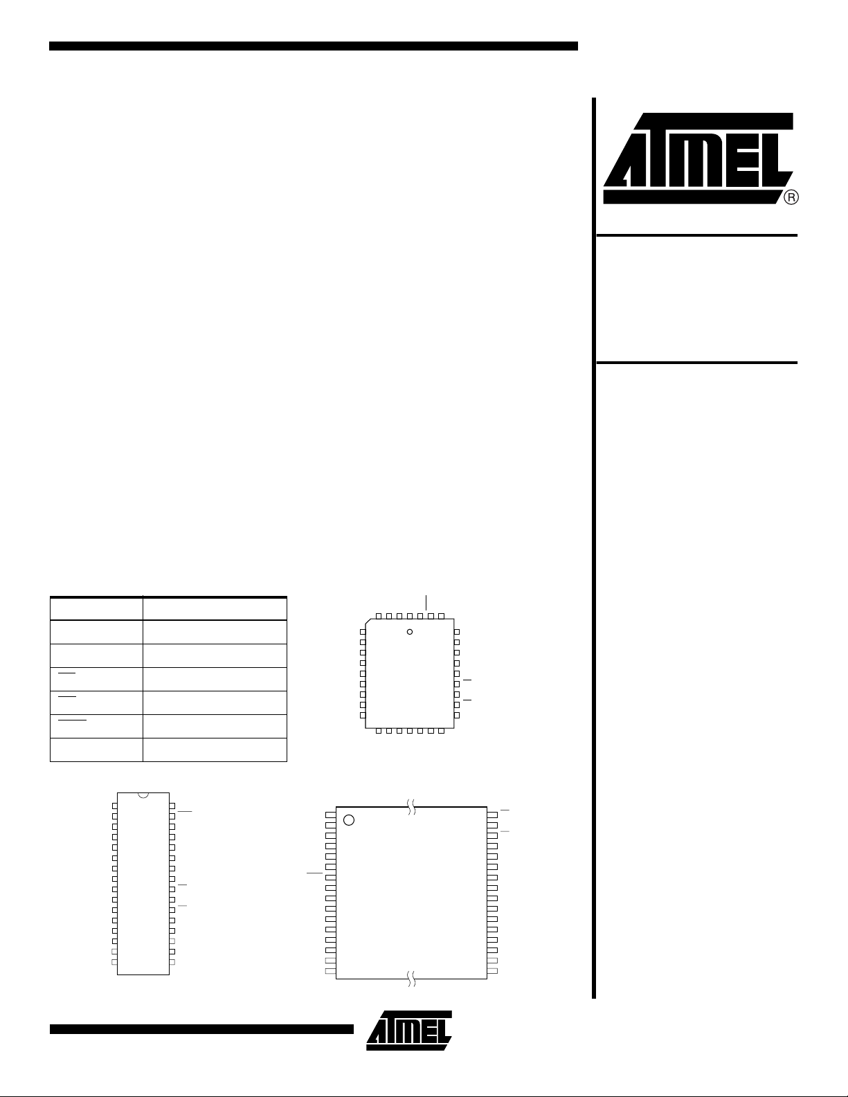
Pin Configurations
Pin Name Function
A0 - A16 Addresses
O0 - O7 Outputs
CE
OE Output En able
PGM
NC No Connect
PDIP Top View
VPP
A16
A15
A12
A7
A6
A5
A4
A3
A2
A1
A0
O0
O1
O2
GND
Chip Enable
Program Strobe
1
32
2
31
3
30
4
29
5
28
6
27
7
26
8
25
9
24
10
23
11
22
12
21
13
20
14
19
15
18
16
17
VCC
PGM
NC
A14
A13
A8
A9
A11
OE
A10
CE
O7
O6
O5
O4
O3
A11
A13
A14
PGM
VCC
VPP
A16
A15
A12
PLCC Top View
A12
A15
A16
VPP
VCC
PGM
NC
432
1
5
A7
6
A6
7
A5
8
A4
9
A3
10
A2
11
A1
12
A0
13
O0
14151617181920
O1
323130
29
A14
28
A13
27
A8
26
A9
25
A11
24
OE
23
A10
22
CE
21
O7
O2
O3O4O5
O6
GND
TSOP Top View
Type 1
1
2
A9
3
A8
4
5
6
NC
7
8
9
10
11
12
13
A7
14
A6
15
A5
16
A4
(continued)
OE
32
A10
31
CE
30
O7
29
O6
28
O5
27
O4
26
O3
25
GND
24
O2
23
O1
22
O0
21
A0
20
A1
19
A2
18
A3
17
AT27C010(L)
1M bit EPROM
Rev. 0321J–07/98
1
Page 2
The AT27C010(L) in available in a choice of industry standard JEDEC-approved one-time programmable (OTP)
plastic PDIP, PL CC, and T SOP packa ges. Al l device s feature two line control (CE
ity to prevent bus contention.
With 128K byte storage capability, the AT27C010(L) allows
firmware to be stored reliably and to be accessed by the
system without the delays of mass storage media.
Atmel’s 27C010 (L) hav e addition al feat ures to ensure hi gh
quality and efficient producti on use. The Rapi d™ Progra mming Algori thm reduc es the time require d to prog ram the
part and guarantees reliable programming. Programming
time is typically on ly 100 µs/ byte. The Inte grated Pr oduct
Identification Code electronica lly identifi es the devic e and
manufacturer. This feature is used by industry standard
programming equi pmen t to se lect the prop er progr ammi ng
algorithms and voltages.
, OE) to give designers th e flexi bil-
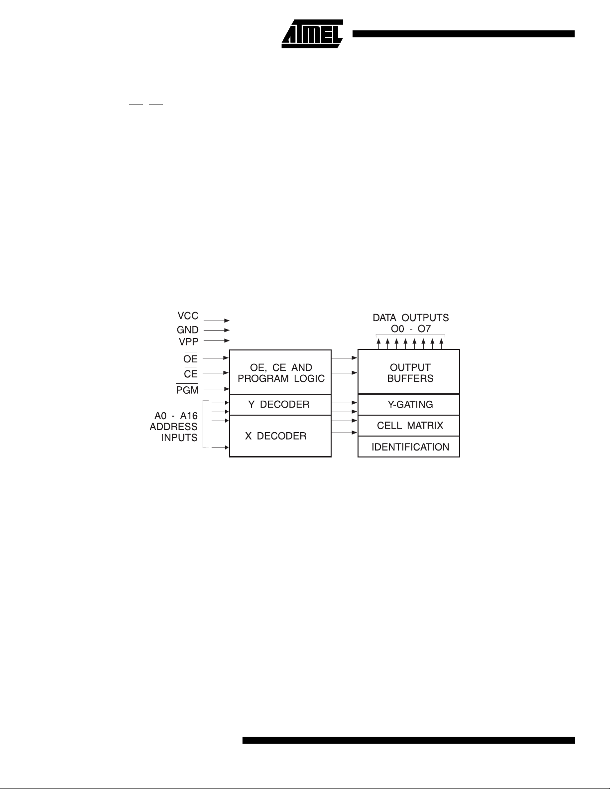
Block Diagram
System Considerations
Switching between active and standby conditions via the
Chip Enable pin may produ ce tra ns ien t vo ltag e ex cu rs i ons .
Unless accommodated by the system design, these transients may exceed data sheet limits, resulting in device
non-conforman ce. At a mini mum, a 0.1 µF high frequency,
low inherent inductance, ceramic capacitor should be utilized for each device. This capacitor should be connected
between the V
close to the device as possible. Additionally, to stabilize the
supply voltage level on printed circuit boards with large
EPROM arrays, a 4.7 µF bulk electrolytic capacitor should
be utilized, again connected between the V
terminals. This capacitor should be positioned as close as
possible to the point where the power supply is connected
to the array.
and Ground terminals of the device, as
CC
and Ground
CC
2
AT27C010(L)
Page 3
Absolute Maximum Ratings*
Temperature Under Bias................................ -55°C to +125°C
Storage Temperature.....................................-65°C to +150°C
Voltage on Any Pin with
Respect to Ground .........................................-2.0V to +7.0V
Voltage on A9 with
Respect to Ground ......................................-2.0V to +14.0V
AT27C010(L)
*NOTICE: Stresses beyond those listed under “Absolute Maxi-
mum Ratings” may cause permanent damage to
the device. This is a stress rating only and functional operation of the device at these or any other
(1)
(1)
conditions beyond those indicated in the operational sections of this specification is not implied.
Exposure to absolute maximum rating conditions
for extended periods may affect device reliability.
VPP Supply Voltage with
Respect to Ground .......................................-2.0V to +14.0V
(1)
Note: 1. Minimum voltage is -0.6V dc which may undershoot to -2.0V for pulses of less than 20 ns. Maximum output pin voltage is
+ 0.75V dc which may overshoot to +7.0 volts for pulses of less than 20 ns.
V
CC
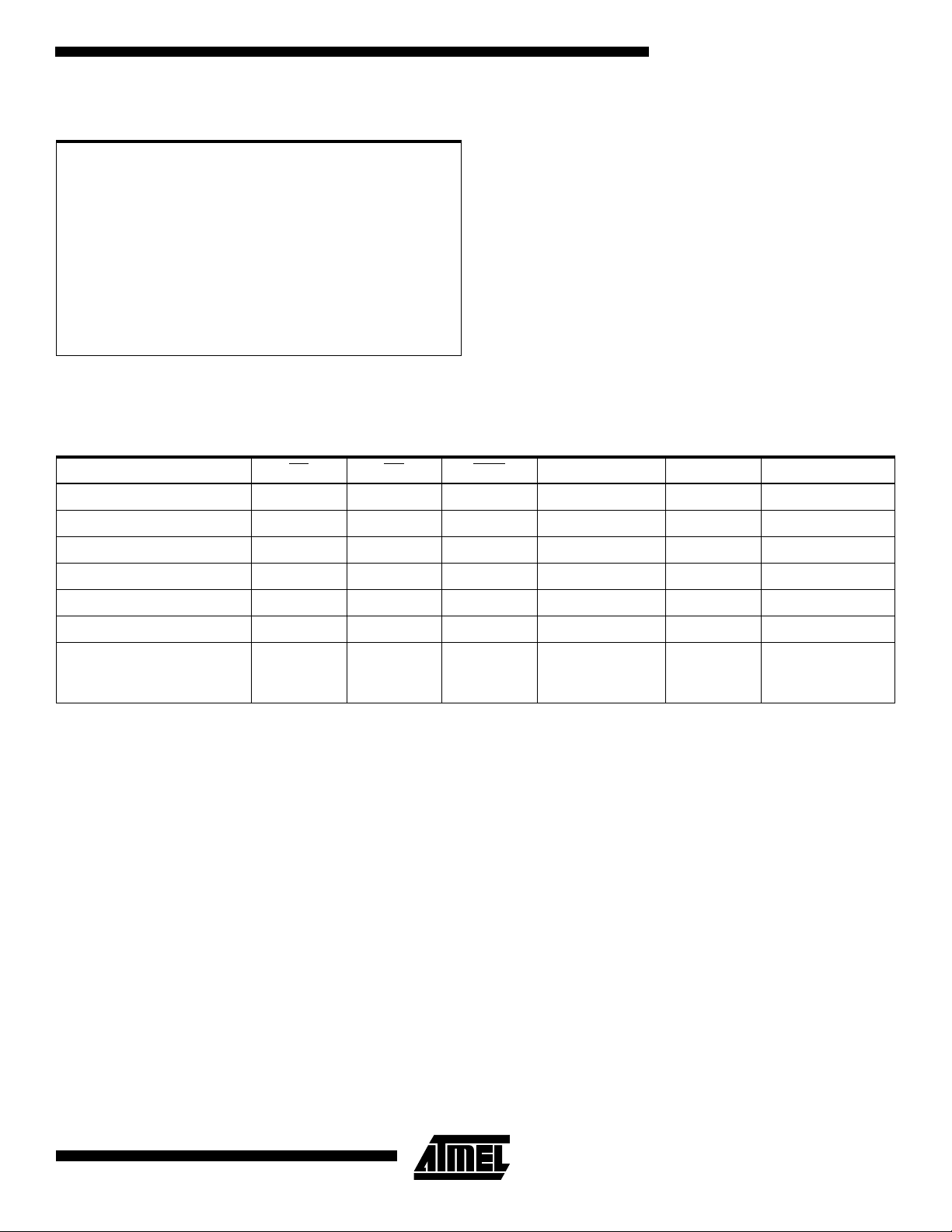
Operating Modes
Mode\Pin CE OE PGM Ai V
Read V
IL
Output Disable X V
Standby V
Rapid Program
(2)
PGM Verify V
PGM Inhibit V
Product Identification
(4)
IH
V
IL
IL
IH
V
IL
V
IL
IH
XXXXHigh Z
V
IH
V
IL
XX X VPPHigh Z
V
IL
(1)
X
Ai X D
XXXHigh Z
V
IL
V
IH
X
Ai V
Ai V
A9 = V
(3)
H
A0 = VIH or VIL
A1 - A16 = V
IL
Notes: 1 . X can be VIL or VIH.
2. Refer to Programming Characteristics.
= 12.0 ± 0.5V.
3. V
H
4. Two identifier bytes may be selected. All Ai inputs are held low (VIL), except A9 which is set to VH and A0 which is toggle d low
) to select the Manufacturer’s Identification byte and high (VIH) to select the Device Code byte.
(V
IL
PP
PP
PP
X Identification Code
D
D
Outputs
OUT
IN
OUT
3
Page 4
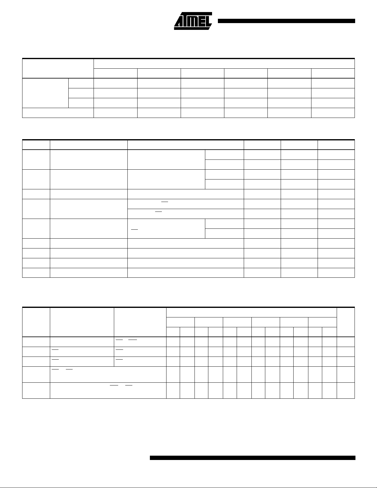
DC and AC Operating Conditions for Read Operation
AT27C010/AT27C010L
-45 -55 -70 -90 -12 -15
°
C - 70°C0
°
C - 85°C-40
Operating
Temp. (Case)
Com. 0°C - 70°C0
Ind. -40°C - 85°C-40
Auto. -40°C - 125°C-40
V
Power Supply 5V ± 10% 5V ± 10% 5V ± 10% 5V ± 10% 5V ± 10% 5V ± 10%
CC
°
C - 70°C0
°
C - 85°C-40
°
C - 70°C0
°
C - 85°C-40
°
C - 70°C0
°
C - 85°C-40
°
C - 125°C-40
°
C - 70°C
°
C - 85°C
°
C - 125°C
DC and Operating Characteristics for Read Operation
Symbol Parameter Condition Min Max Units
I
LI
I
LO
(2)
IPP1
I
SB
I
CC
V
IL
V
IH
V
OL
V
OH
Input Load Current VIN = 0V to V
CC
Auto.
Com., Ind.
Com., Ind.
Output Leakage Current V
(1))
V
Read/Standby Current VPP = V
PP
(1)
V
Standby Current
CC
VCC Active Current
= 0V to V
OUT
(CMOS), CE = V
I
SB1
I
(TTL), CE = 2.0 to VCC + 0.5V 1 mA
SB2
f = 5 MHz, I
= V
CE
CC
CC
± 0.3V 100 µA
CC
= 0 mA,
OUT
IL
Auto.
AT27C010(L) 25 mA
AT27C010 35 mA
Input Low Voltage -0.6 0.8 V
Input High Voltage 2.0 V
Output Low Voltage IOL = 2.1 mA 0.4 V
Output High Voltage I
= -400 µA2.4V
OH
±
1µA
±
5µA
±
5µA
±
10 µA
10 µA
+ 0.5 V
CC
Notes: 1. VCC must be applied simultaneously or before VPP, and removed simultaneously or after VPP..
may be connected directly to VCC, except d uring p r og r amming. The suppl y c urre nt w o ul d th en be the sum of ICC and IPP..
2. V
PP
AC Characteristics for Read Operat ion
Symbol Parameter Condition
t
t
t
t
t
ACC
CE
OE
DF
OH
(3)
(2)
(2)(3)
(4)(5)
Address to Output Delay CE =OE=V
CE to Output Delay OE = V
OE to Output Delay CE = V
IL
IL
IL
OE or CE High to Output Float, whichever occurred
first
Output Hold from Address, CE or OE, whichever
occurred first
Notes: 2,3,4,5. - see AC Waveforms for Read Operation.
4
AT27C010(L)
AT27C010/AT27C010L
-45 -55 -70 -90 -12 -15
Min Max Min Max Min Max Min Max Min Max Min Max
Units
45 55 70 90 120 150 ns
45 55 70 90 120 150 ns
20 25 30 35 35 40 ns
20 20 25 25 30 35 ns
777000ns
Page 5
AT27C010(L)
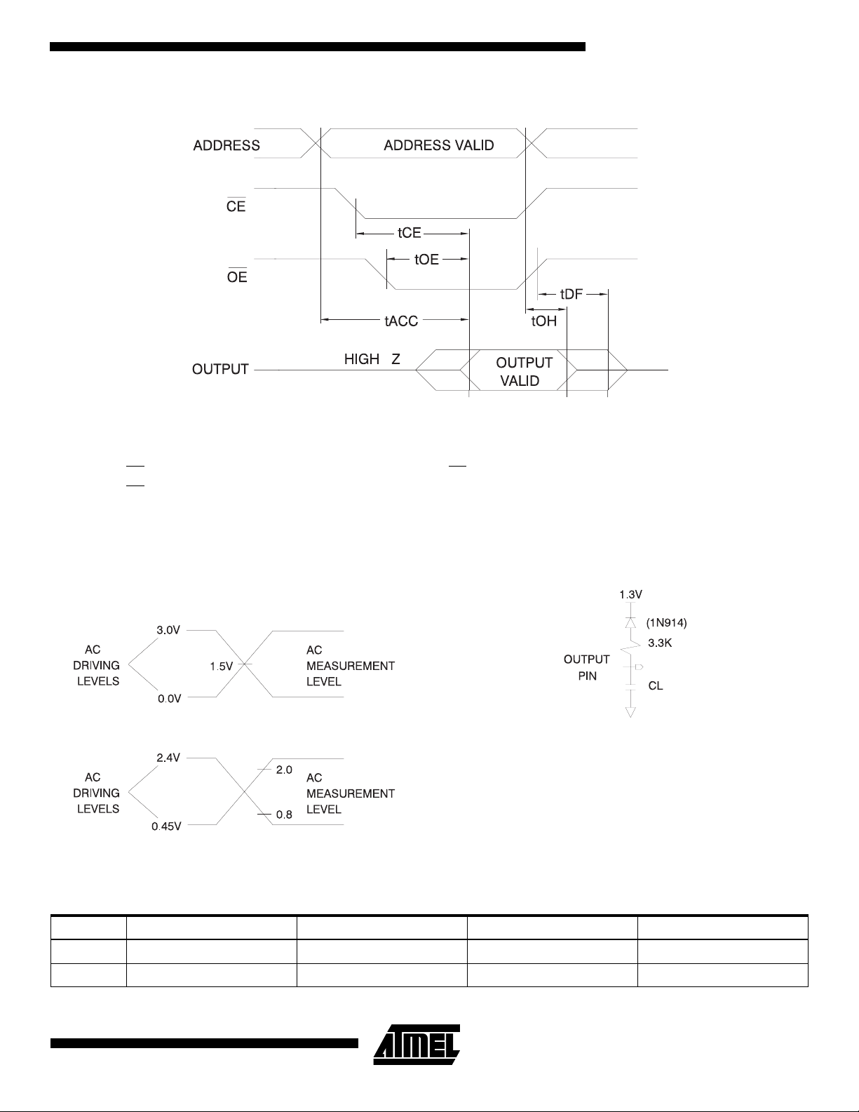
AC Waveforms for Read Operation
Notes: 1. Timing measurement reference level is 1.5V for -45 and -55 devices. Input AC drive levels are VIL = 0.0V and VIH = 3.0V.
Timing measurement reference levels for all other speed grades are V
= 0.45V and VIH = 2.4V.
V
IL
2. OE may be delayed up to tCE - tOE after the falling edge of CE without impact on tCE.
3. OE
4. This parameter is only sampled and is not 100% tested.
5. Output float is defined as the point when data is no longer driven.
may be delayed up to t
- tOE after the address is valid without impact on t
ACC
(1)
= 0.8V and VOH = 2.0V. Input AC drive levels are
OL
.
ACC
Input Test Waveforms and
Output Test Load
Measurement Levels
For -45 and -55 devices only:
tR, tF < 5 ns (10% to 90%)
For -70, -90, -12, -15, and -20 devices:
tR, tF < 20 ns (10% to 90%)
Note: CL = 100 pF including jig
capacitanc e, except for
the -45 and -55 devices,
where C
=30pF.
L
Pin Capacitance
f = 1 MHz, T = 25°C
Symbol Ty p Max Units Conditions
C
IN
C
OUT
Note: 1. Typical values for nominal supply voltage. This parameter is only sampled and is not 100% tested.
(1)
48pFV
812pFV
IN
OUT
= 0V
= 0V
5
Page 6

Programming Waveforms
(1)
Notes: 1. The Input Timing Reference is 0.8V for VIL and 2.0V for VIH.
2. t
OE
and t
are characteristics of the device but must be accommodated by the programmer.
DFP
3. When programming the AT27C010(L) at 0.1 µF capacitor is required across VPP and ground to suppress spurious voltage
transients.
DC Programming Characteristics
TA = 25 ± 5°C, VCC = 6.5 ± 0.25V, VPP = 13.0 ± 0.25V
Symbol Parameter T est Condit ions
I
LI
V
IL
V
IH
V
OL
V
OH
I
CC2
I
PP2
V
ID
Input Load Current VIN = VIL, V
IH
Input Low Level -0.6 0.8 V
Input High Level 2.0 VCC + 1 V
Output Low Voltage IOL = 2.1 mA 0.4 V
Output High Voltage IOH = -400 µA2.4 V
VCC Supply Current (Program and Verify) 40 mA
VPP Supply Current CE = PGM = V
A9 Product Identification Voltage 11.5 12.5 V
Limits
UnitsMin Max
10
±
IL
20 mA
A
µ
6
AT27C010(L)
Page 7

AC Programming Characteristics
TA = 25 ± 5°C, VCC = 6.5 ± 0.25 V, VPP = 13.0 ± 0.25V
Symbol Parameter T est Condit ions
AT27C010(L)
Limits
(1)
UnitsMin Max
t
AS
t
CES
t
OES
t
DS
t
AH
t
DH
t
DFP
t
VPS
t
VCS
t
PW
t
OE
t
PRT
Address Setup Time
CE Setup Time 2 µs
OE Setup Time 2 µs
Data Setup Time 2 µs
Address Hold Time 0 µs
Data Hold Time 2 µs
OE High to Output Float Delay
(2)
VPP Setup Time 2 µs
Input Rise and Fall Times
(10% to 90%) 20ns
Input Pulse Levels
0.45V to 2.4V
Input Timing Reference Level
0.8V to 2.0 V
VCC Setup Time 2 µs
PGM Program Pulse Width
(3)
Data Valid from OE 150 ns
Output Timing Reference Level
0.8V to 2.0 V
VPP Pulse Rise TIme
During Programming
2 µs
0 130 ns
95 105 µs
50 ns
Notes: 1. VCC must be applied simultaneously or before VPP and removed simultaneously or after VPP..
2. This parameter is only sample d and i s not 1 00% te sted. O utput Float i s defi ned as the po int wh ere dat a is no longe r driv en—
see timing diagram.
3. Program Pulse width tolerance is 100 µsec ± 5%.
Atmel’s 27C010(L) Integrated Product Identification Code
Pins
Codes
Hex
DataA0 O7 O6 O5 O4 O3 O2 O1 O0
Manufacturer 000011110 1E
Device Type 100000101 05
7
Page 8

Rapid Programming Algorithm
A 100 µs PGM pulse width is used to program. The
address is set to the first location. V
is raised to 13.0V. Eac h address i s first program med
V
PP
with one 100 µs PGM
verification / reprogramming loop is executed for each
address. In the event a byte fails to pa ss verificat ion, up to
10 successive 100 µs pulses are applied with a v erifica tion
pulse without verificat ion. Then a
is raised to 6.5V and
CC
after each pulse. If the byte fails to verify after 10 pulses
have been applied, the part is consi dered failed. After the
byte verifies properly, the next address is selected until all
have been checked. V
5.0V. All bytes are read again and compared wi th th e original data to determine if the device passes or fails.
is then lowered to 5.0V and VCC to
PP
8
AT27C010(L)
Page 9

AT27C010 Ordering Information
I
t
ACC
(ns)
45 35 0.1 AT27C010-45JC
55 35 0.1 AT27C010-55JC
70 35 0.1 AT27C010-70JC
(mA)
CC
Ordering Code Package Operation RangeActive Standby
AT27C010-45PC
AT27C010-45TC
35 0.1 AT27C010-45JI
AT27C010-45PI
AT27C010-45TI
AT27C010-55PC
AT27C010-55TC
35 0.1 AT27C010-55JI
AT27C010-55PI
AT27C010-55TI
AT27C010-70PC
AT27C010-70TC
35 0.1 AT27C010-70JI
AT27C010-70PI
AT27C010-70TI
32J
32P6
32T
32J
32P6
32T
32J
32P6
32T
32J
32P6
32T
32J
32P6
32T
32J
32P6
32T
AT27C010(L)
Commercial
(0°C to 70°C)
Industrial
(-40°C to 85°C)
Commercial
(0°C to 70°C)
Industrial
(-40°C to 85°C)
Commercial
(0°C to 70°C)
Industrial
(-40°C to 85°C)
Package Type
(continued)
32J 32-Lead, Plastic J-Leaded Chip Carrier (PLCC)
32P6 32-Lead, 0.600" Wide, Plastic Dual Inline Package (PDIP)
32T 32-Lead, Plastic Thin Small Outline Package (TSOP)
9
Page 10

AT27C010 Ordering Information (Continued)
I
t
ACC
(ns)
90 35 0.1 AT27C010-90JC
120 35 0.1 AT27C010-12JC
150 35 0.1 AT27C010-15JC
(mA)
CC
Ordering Code Package Operation RangeActive Standby
AT27C010-90PC
AT27C010-90TC
35 0.1 AT27C010-90JI
AT27C010-90PI
AT27C010-90TI
35 0.1 AT27C010-90JA
AT27C010-90PA
AT27C010-12PC
AT27C010-12TC
35 0.1 AT27C010-12JI
AT27C010-12PI
AT27C010-12TI
35 0.1 AT27C010-12JA
AT27C010-12PA
AT27C010-15PC
AT27C010-15TC
35 0.1 AT27C010-15JI
AT27C010-15PI
AT27C010-15TI
35 0.1 AT27C010-15JA
AT27C010-15PA
32J
32P6
32T
32J
32P6
32T
32J
32P6
32J
32P6
32T
32J
32P6
32T
32J
32P6
32J
32P6
32T
32J
32P6
32T
32J
32P6
Commercial
(0°C to 70°C)
Industrial
(-40°C to 85°C)
Automotive
(-40°C to 125°C)
Commercial
(0°C to 70°C)
Industrial
(-40°C to 85°C)
Automotive
(-40°C to 125°C)
Commercial
(0°C to 70°C)
Industrial
(-40°C to 85°C)
Automotive
(-40°C to 125°C)
Package Type
32J 32-Lead, Plastic J-Leaded Chip Carrier (PLCC)
32P6 32-Lead, 0.600" Wide, Plastic Dual Inline Package (PDIP)
32T 32-Lead, Plastic Thin Small Outline Package (TSOP)
10
AT27C010(L)
Page 11

AT27C010L Ordering Information
I
t
ACC
(ns)
45 25 0.1 AT27C010L-45JC
55 25 0.1 AT27C010L-55JC
70 25 0.1 AT27C010L-70JC
90 25 0.1 AT27C010L-90JC
120 25 0.1 AT27C010L-12JC
150 25 0.1 AT27C010L-15JC
(mA)
CC
Ordering Code Package Operation RangeActive Standby
AT27C010L-45PC
AT27C010L-45TC
25 0.1 AT27C010L-45JI
AT27C010L-45PI
AT27C010L-45TI
AT27C010L-55PC
AT27C010L-55TC
25 0.1 AT27C010L-55JI
AT27C010L-55PI
AT27C010L-55TI
AT27C010L-70PC
AT27C010L-70TC
25 0.1 AT27C010L-70JI
AT27C010L-70PI
AT27C010L-70TI
AT27C010L-90PC
AT27C010L-90TC
25 0.1 AT27C010L-90JI
AT27C010L-90PI
AT27C010L-90TI
AT27C010L-12PC
AT27C010L-12TC
25 0.1 AT27C010L-12JI
AT27C010L-12PI
AT27C010L-12TI
AT27C010L-15PC
AT27C010L-15TC
25 0.1 AT27C010L-15JI
AT27C010L-15PI
AT27C010L-15TI
32J
32P6
32T
32J
32P6
32T
32J
32P6
32T
32J
32P6
32T
32J
32P6
32T
32J
32P6
32T
32J
32P6
32T
32J
32P6
32T
32J
32P6
32T
32J
32P6
32T
32J
32P6
32T
32J
32P6
32T
AT27C010(L)
Commercial
(0°C to 70°C)
Industrial
(-40°C to 85°C)
Commercial
(0°C to 70°C)
Industrial
(-40°C to 85°C)
Commercial
(0°C to 70°C)
Industrial
(-40°C to 85°C)
Commercial
(0°C to 70°C)
Industrial
(-40°C to 85°C)
Commercial
(0°C to 70°C)
Industrial
(-40°C to 85°C)
Commercial
(0°C to 70°C)
Industrial
(-40°C to 85°C)
Package Type
32J 32-Lead, Plastic J-Leaded Chip Carrier (PLCC)
32P6 32-Lead, 0.600" Wide, Plastic Dual Inline Package (PDIP)
32T 32-Lead, Plastic Thin Small Outline Package (TSOP)
11
Page 12

Packaging Information
32J
, 32-Lead, Plastic J-Leaded Chip Carrier (PLCC)
Dimensions in Inches and (Millimeters)
JEDEC STANDARD MS-016 AE
.045(1.14) X 45˚
.032(.813)
.026(.660)
.050(1.27) TYP
.453(11.5)
.447(11.4)
.495(12.6)
.485(12.3)
PIN NO.1
IDENTIFY
.553(14.0)
.547(13.9)
.300(7.62) REF
.430(10.9)
.390(9.90)
.025(.635) X 30˚ - 45˚
.595(15.1)
.585(14.9)
AT CONTACT
POINTS
.022(.559) X 45˚ MAX (3X)
.012(.305)
.008(.203)
.021(.533)
.013(.330)
.030(.762)
.015(.381)
.095(2.41)
.060(1.52)
.140(3.56)
.120(3.05)
.530(13.5)
.490(12.4)
32P6
, 32-Lead, 0.600" Wide, Plastic Dual Inline
Package (PDIP)
Dimensions in Inches and (Millimeters)
1.67(42.4)
.220(5.59)
SEATING
PLANE
MAX
.161(4.09)
.125(3.18)
.110(2.79)
.090(2.29)
.012(.305)
.008(.203)
1.64(41.7)
1.500(38.10) REF
.065(1.65)
.041(1.04)
.630(16.0)
.590(15.0)
.690(17.5)
.610(15.5)
PIN
1
0
REF
15
.566(14.4)
.530(13.5)
.090(2.29)
.005(.127)
.065(1.65)
.015(.381)
.022(.559)
.014(.356)
MAX
MIN
32T
, 32-Lead, Plastic Thin Small Outline Package
(TSOP)
Dimensions in Millimeters and (Inches)*
JEDEC OUTLINE MO-142 BD
INDEX
MARK
0.50(.020)
BSC
0
REF
5
7.50(.295)
REF
8.20(.323)
7.80(.307)
0.15(.006)
0.05(.002)
18.5(.728)
18.3(.720)
0.25(.010)
0.15(.006)
0.70(.028)
0.50(.020)
20.2(.795)
19.8(.780)
1.20(.047) MAX
*Controlling dimension: millimeters
0.20(.008)
0.10(.004)
12
AT27C010(L)
Page 13

AT27C010(L)
13
Page 14

14
AT27C010(L)
Page 15

AT27C010(L)
15
Page 16

Atmel Headquarters Atmel Operations
Corporate Headquarters
2325 Orchard Parkway
San Jose, CA 95131
TEL (408) 441- 0311
FAX (408) 487-2600
Europe
Atmel U.K., Ltd.
Coliseum Business Centre
Riverside Way
Camberley, Surrey GU15 3YL
England
TEL (44) 1276-686677
FAX (44) 1276-686697
Asia
Atmel Asia, Ltd.
Room 1219
Chinachem Golden Plaza
77 Mody Road
Tsimshatsui East
Kowloon, Hong Kong
TEL (852) 27219778
FAX (852) 27221369
Japan
Atmel Japan K.K.
Tonetsu Shinkawa Bldg., 9F
1-24-8 Shinka wa
Chuo-ku, Tokyo 104-0033
Japan
TEL (81) 3-3523-3551
FAX (81) 3-3523-7581
Atmel Colorado Springs
1150 E. Cheyenne Mtn. Blvd.
Colorado Springs, CO 80906
TEL (719) 576-3300
FAX (719) 540-1759
Atmel Rousset
Zone Indu strie lle
13106 Rousset Cedex, France
TEL (33) 4 42 53 60 00
FAX (33) 4 42 53 60 01
Fax-on-Demand
North America:
1-(800) 292-8635
International:
1-(408) 441-0732
e-mail
literature@atmel.com
Web Site
http://www.atmel.com
BBS
1-(408) 436-4309
© Atmel Corporation 1998.
Atmel Corporation makes no warranty for the use of its products, other than those expressly contained in the Company’s standard warranty which is detailed in Atmel’s Terms and Conditions located on the Company’s website. The Company assumes no responsibility for
any errors which may appear in this document, reserves the right to change devices or specifications detailed herein at any time without
notice, and does not make any commitment to update the information contained herein. No licenses to patents or other intellectual property of Atmel are granted by the Company in connection with the sale of Atmel products, expressly or by implication. Atmel’s products are
not authorized for use as critical components in life support devices or systems.
®
Marks bearing
Terms and product names in this document may be trademarks of others.
and/or ™ are registered trademarks and trademarks of Atmel Corporation.
Printed on recycled paper.
0321J–07/98/xM
 Loading...