

Page 1
Features
• Serial Peripheral Interface (SPI) Compatible
• Supports SPI Modes 0 (0,0) and 3 (1,1)
– Datasheet Describes Mode 0 Operation
• 20 MHz Clock Rate
• Byte Mode and 256-byte Page Mode for Program Operations
• Sector Architecture:
– Four Sectors with 32K Bytes Each (1M)
– 128 Pages per Sector
• Product Identification Mode
• Low-voltage Operation
– 2.7 (V
• Sector Write Protection
• Write Protect (WP) Pin and Write Disable Instructions for
both Hardware and Software Data Protection
• Self-timed Program Cycle (20 µs/Byte Typical)
• Self-timed Sector Erase Cycle (1 second/Sector Typical)
• Single Cycle Reprogramming (Erase and Program) for Status Register
• High Reliability
– Endurance: 10,000 Write Cycles Typical
• Lead-free/Halogen-free Devices
• 8-lead JEDEC SOIC and 8-lead SAP Packages
= 2.7V to 3.6V)
CC
SPI Serial
Memory
1M (131,072 x 8)
AT25F1024A
Description
The AT25F1024A provides 1,048,576 bits of serial reprogrammable Flash memory
organized as 131,072 words of 8 bits each. The device is optimized for use in many
industrial and commercial applications where low-power and low-voltage operation
are essential. The AT25F1024A is available in a space-saving 8-lead JEDEC SOIC
and 8-lead SAP packages.
The AT25F1024A is enabled through the Chip Select pin (CS
wire interface consisting of Serial Data Input (SI), Serial Data Output (SO), and Serial
Clock (SCK). All write cycles are completely self-timed.
BLOCK WRITE protection for top 1/4, top 1/2 or the entire memory array is enabled by
programming the status register. Separate write enable and write disable instructions
are provided for additional data protection. Hardware data protection is provided via
the WP
HOLD
pin to protect against inadvertent write attempts to the status register. The
pin may be used to suspend any serial communication without resetting the
serial sequence.
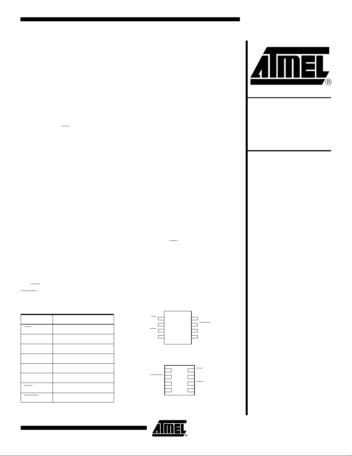
Pin Configurations
Pin Name Function
CS
SCK Serial Data Clock
SI Serial Data Input
SO Serial Data Output
GND Ground
VCC Power Supply
WP
HOLD
Chip Select
Write Protect
Suspends Serial Input
CS
SO
WP
GND
VCC
HOLD
SCK
SI
) and accessed via a 3-
8-lead SOIC
1
2
3
4
8-lead SAP
8
7
6
5
Bottom View
VCC
8
HOLD
7
SCK
6
SI
5
CS
1
SO
2
WP
3
GND
4
Advance
Information
Rev. 3346C–SEEPR–7/04
1
Page 2
Absolute Maximum Ratings*
Operating Temperature .................................... -40°C to +85°C
Storage Temperature..................................... -65°C to +150°C
Voltage on Any Pin
with Respect to Ground .....................................-1.0V to +3.6V
Maximum Operating Voltage ............................................ 3.6V
DC Output Current........................................................ 5.0 mA
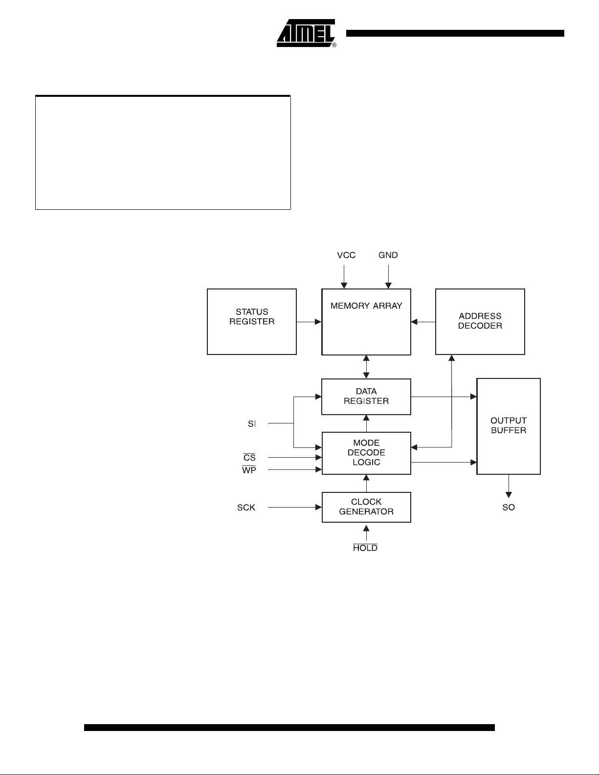
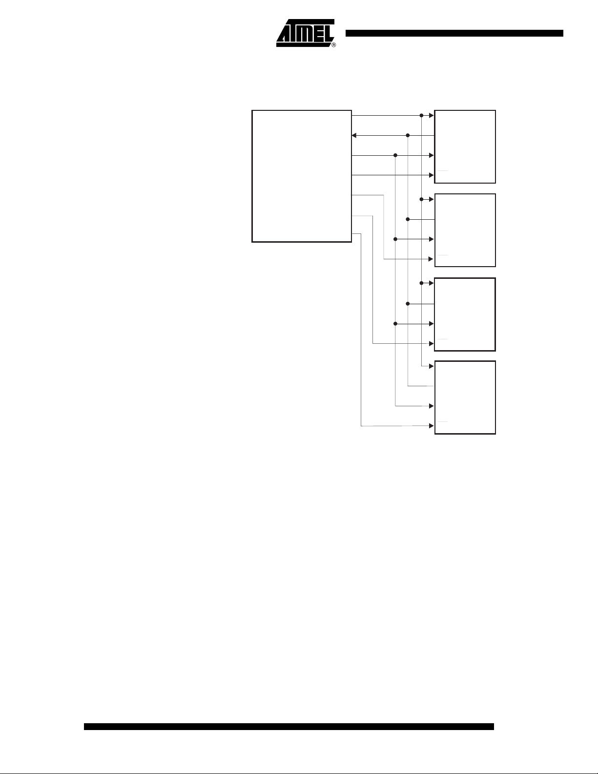
Block Diagram
*NOTICE: Stresses beyond those listed under “Absolute
Maximum Ratings” may cause permanent damage to the device. This is a stress rating only and
functional operation of the device at these or any
other conditions beyond those indicated in the
operational sections of this specification is not
implied. Exposure to absolute maximum rating
conditions for extended periods may affect
device reliability.
131,072 x 8
2
3346C–SEEPR–7/04
Page 3
Pin Capacitance
(1)
Applicable over recommended operating range from TA = 25°C, f = 20.0 MHz, VCC = +3.6V (unless otherwise noted).
Symbol Test Conditions Max Units Conditions
C
OUT
C
IN
Output Capacitance (SO) 8 pF V
Input Capacitance (CS, SCK, SI, WP, HOLD)6pFV
OUT
IN
= 0V
= 0V
Note: 1. This parameter is characterized and is not 100% tested.
DC Characteristics (Preliminary – Subject to Change)
Applicable over recommended operating range from: TAI = -40 to +85°C, VCC = +2.7 to +3.6V,
T
= 0 to +70°C, VCC = +2.7 to +3.6V (unless otherwise noted).
AC
Symbol Parameter Test Condition Min Typ Max Units
V
CC
I
CC1
I
CC2
I
SB
I
IL
I
OL
(1)
V
IL
(1)
V
IH
V
OL
V
OH
Note: 1. V
Supply Voltage 2.7 3.6 V
Supply Current VCC = 3.6V at 20 MHz, SO = Open Read 10.0 15.0 mA
Supply Current VCC = 3.6V at 20 MHz, SO = Open Write 25.0 35.0 mA
Standby Current VCC = 2.7V, CS = V
Input Leakage VIN = 0V to V
CC
CC
-3.0 3.0 µA
2.0 10.0 µA
Output Leakage VIN = 0V to VCC, TAC = 0°C to 70°C -3.0 3.0 µA
Input Low Voltage -0.6 V
x 0.3 V
CC
Input High Voltage VCC x 0.7 VCC + 0.5 V
Output Low Voltage
Output High Voltage IOH = -100 µA VCC - 0.2 V
2.7V ≤ V
and VIH max are reference only and are not tested.
IL
≤ 3.6V
CC
I
= 0.15 mA 0.2 V
OL
3346C–SEEPR–7/04
3
Page 4
AC Characteristics (Preliminary – Subject to Change)
Applicable over recommended operating range from TA = -40 to +85°C, VCC = +2.7 to +3.6V
C
= 1 TTL Gate and 30 pF (unless otherwise noted).
L
Symbol Parameter Min Typ Max Units
f
SCK
t
RI
t
FI
t
WH
t
WL
t
CS
t
CSS
t
CSH
t
SU
t
H
t
HD
t
CD
t
V
t
HO
t
LZ
t
HZ
t
DIS
t
EC
t
SR
t
BPC
Endurance
(2)
SCK Clock Frequency 0 20 MHz
Input Rise Time 20 ns
Input Fall Time 20 ns
SCK High Time 20 ns
SCK Low Time 20 ns
CS High Time 25 ns
CS Setup Time 25 ns
CS Hold Time 25 ns
Data In Setup Time 5 ns
Data In Hold Time 5 ns
Hold Setup Time 15 ns
Hold Time 15 ns
Output Valid 20 ns
Output Hold Time 0 ns
Hold to Output Low Z 200 ns
Hold to Output High Z 200 ns
Output Disable Time 100 ns
Erase Cycle Time per Sector 1.1 s
Status Register Write Cycle Time 60 ms
Byte Program Cycle Time
(1)
Notes: 1. The programming time for n bytes will be equal to n x t
2. This parameter is characterized at 3.3V, 25°C and is not 100% tested.
3. One write cycle consists of erasing a sector, followed by programming the same sector.
BPC
20 60 µs
10K Write Cycles
(3)
.
4
3346C–SEEPR–7/04
Page 5

Serial Interface
MASTER: The device that generates the serial clock.
Description
SLAVE: Because the Serial Clock pin (SCK) is always an input, the AT25F1024A
always operates as a slave.
TRANSMITTER/RECEIVER: The AT25F1024A has separate pins designated for data
transmission (SO) and reception (SI).
MSB: The Most Significant Bit (MSB) is the first bit transmitted and received.
SERIAL OP-CODE: After the device is selected with CS
received. This byte contains the op-code that defines the operations to be performed.
INVALID OP-CODE: If an invalid op-code is received, no data will be shifted into the
AT25F1024A, and the serial output pin (SO) will remain in a high impedance state until
the falling edge of CS
CHIP SELECT: The AT25F1024A is selected when the CS
is not selected, data will not be accepted via the SI pin, and the serial output pin (SO)
will remain in a high impedance state.
HOLD: The HOLD
When the device is selected and a serial sequence is underway, HOLD
pause the serial communication with the master device without resetting the serial
sequence. To pause, the HOLD
resume serial communication, the HOLD
(SCK may still toggle during HOLD
is in the high impedance state.
WRITE PROTECT: The AT25F1024A has a write lockout feature that can be activated
by asserting the write protect pin (WP
sectors will be READ only. The write protect pin will allow normal read/write operations
when held high. When the WP
the status register are inhibited. WP
the status register. If the internal status register write cycle has already been initiated,
WP
going low will have no effect on any write operation to the status register. The WP
pin function is blocked when the WPEN bit in the status register is “0”. This will allow the
user to install the AT25F1024A in a system with the WP
able to write to the status register. All WP
is set to “1”.
is detected again. This will reinitialize the serial communication.
pin is used in conjunction with the CS pin to select the AT25F1024A.
pin must be brought low while the SCK pin is low. To
pin is brought high while the SCK pin is low
). Inputs to the SI pin will be ignored while the SO pin
). When the lockout feature is activated, locked-out
is brought low and WPEN bit is “1”, all write operations to
going low while CS is still low will interrupt a write to
pin functions are enabled when the WPEN bit
going low, the first byte will be
pin is low. When the device
can be used to
pin tied to ground and still be
3346C–SEEPR–7/04
5
Page 6
SPI Serial Interface
MASTER:
MICROCONTROLLER
DATA OUT (MOSI)
DATA IN (MISO)
SERIAL CLOCK (SPI CK)
SS0
SS1
SS2
SS3
SLAVE:
AT25F1024A
SI
SO
SCK
CS
SI
SO
SCK
CS
SI
SO
SCK
CS
SI
SO
SCK
CS
6
3346C–SEEPR–7/04
Page 7
Functional Description
The AT25F1024A is designed to interface directly with the synchronous serial peripheral
interface (SPI) of the 6800 type series of microcontrollers.
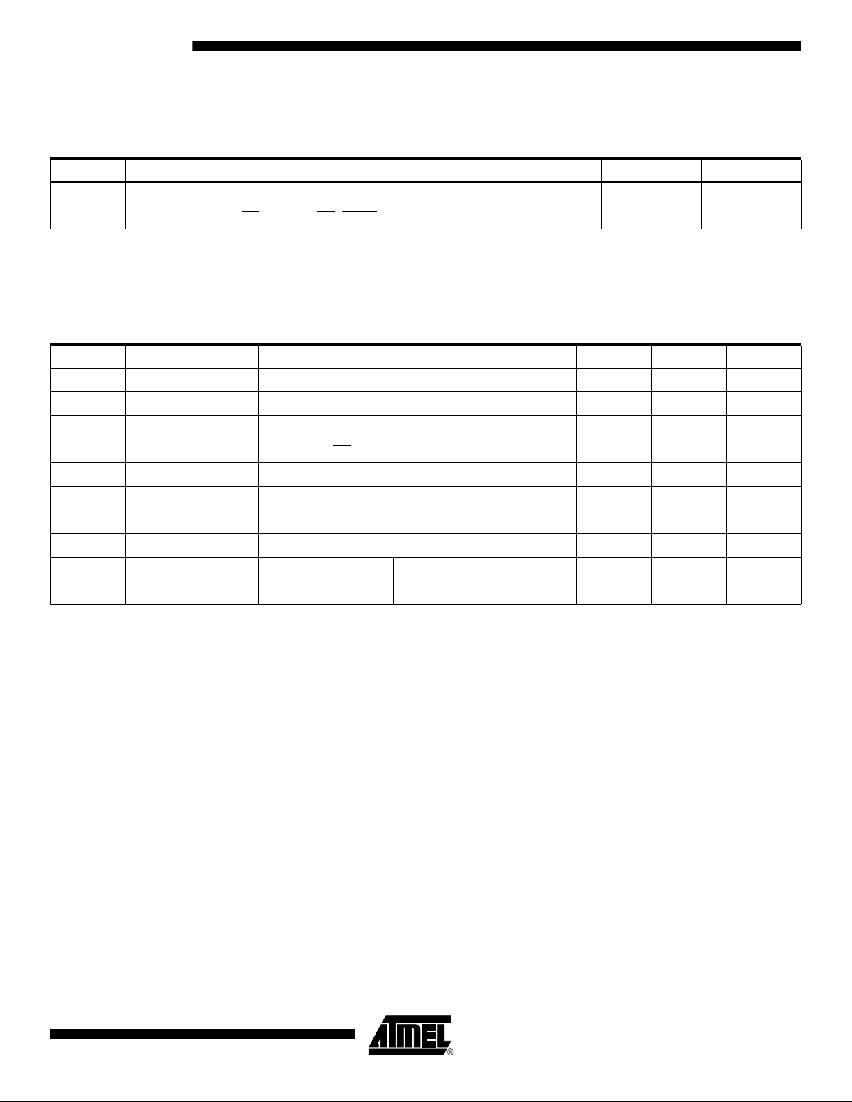
The AT25F1024A utilizes an 8-bit instruction register. The list of instructions and their
operation codes are contained in Table 1. All instructions, addresses, and data are
transferred with the MSB first and start with a high-to-low transition.
Write is defined as program and/or erase in this specification. The following commands,
PROGRAM, SECTOR ERASE, CHIP ERASE, and WRSR are write instructions for
AT25F1024A.
Table 1. Instruction Set for the AT25F1024A
Instruction
Instruction Name
WREN 0000 X110 Set Write Enable Latch
WRDI 0000 X100 Reset Write Enable Latch
RDSR 0000 X101 Read Status Register
WRSR 0000 X001 Write Status Register
READ 0000 X011 Read Data from Memory Array
PROGRAM 0000 X010 Program Data Into Memory Array
SECTOR ERASE 0101 X010 Erase One Sector in Memory Array
CHIP ERASE 0110 X010 Erase All Sectors in Memory Array
Format Operation
RDID 0001 X101 Read Manufacturer and Product ID
WRITE ENABLE (WREN): The device will power up in the write disable state when V
CC
is applied. All write instructions must therefore be preceded by the WREN instruction.
WRITE DISABLE (WRDI): To protect the device against inadvertent writes, the WRDI
instruction disables all write commands. The WRDI instruction is independent of the status of the WP
pin.
READ STATUS REGISTER (RDSR): The RDSR instruction provides access to the status register. The READY/BUSY and write enable status of the device can be determined
by the RDSR instruction. Similarly, the Block Write Protection bits indicate the extent of
protection employed. These bits are set by using the WRSR instruction. During internal
write cycles, all other commands will be ignored except the RDSR instruction.
Table 2. Status Register Format
Bit 7 Bit 6 Bit 5 Bit 4 Bit 3 Bit 2 Bit 1 Bit 0
WPEN X X X BP1 BP0 WEN RDY
3346C–SEEPR–7/04
7
Page 8

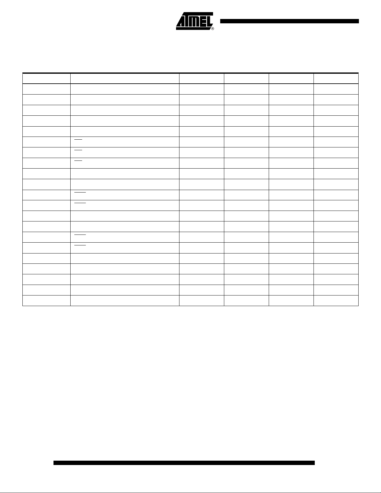
Table 3. Read Status Register Bit Definition
Bit Definition
Bit 0 (RDY
Bit 1 (WEN)
Bit 2 (BP0) See Table 4.
Bit 3 (BP1) See Table 4.
Bits 4-6 are 0s when device is not in an internal write cycle.
Bit 7 (WPEN) See Table 5.
Bits 0-7 are 1s during an internal write cycle.
)
Bit 0 = 0 (RDY
write cycle is in progress.
Bit 1 = 0 indicates the device
the device is WRITE ENABLED.
) indicates the device is READY. Bit 0 = 1 indicates the
is not
WRITE ENABLED. Bit 1 = 1 indicates
READ PRODUCT ID (RDID): The RDID instruction allows the user to read the manufacturer and product ID of the device. The first byte after the instruction will be the
manufacturer code (1FH = ATMEL), followed by the device code, 60H.
WRITE STATUS REGISTER (WRSR): The WRSR instruction allows the user to select
one of four levels of protection for the AT25F1024A. The AT25F1024A is divided into
four sectors where the top quarter (1/4), top half (1/2), or all of the memory sectors can
be protected (locked out) from write. Any of the locked-out sectors will therefore be
READ only. The locked-out sector and the corresponding status register control bits are
shown in Table 4.
The three bits, BP0, BP1, and WPEN, are nonvolatile cells that have the same properties and functions as the regular memory cells (e.g., WREN, t
, RDSR).
WC
Table 4. Block Write Protect Bits
Status Register Bits AT25F1024A
Array Addresses
Level
000None None
1(1/4) 0 1 018000 - 01FFFF Sector 4
2(1/2) 1 0 010000 - 01FFFF Sector 3, 4
3(All) 1 1 000000 - 01FFFF
BP1 BP0
Locked Out
Locked-out
Sector(s)
All sectors
(1 - 4)
8
3346C–SEEPR–7/04
Page 9

The WRSR instruction also allows the user to enable or disable the Write Protect (WP)
pin through the use of the Write Protect Enable (WPEN) bit. Hardware write protection is
enabled when the WP
disabled when either the WP
pin is low and the WPEN bit is “1”. Hardware write protection is
pin is high or the WPEN bit is “0.” When the device is hardware write protected, writes to the Status Register, including the Block Protect bits and
the WPEN bit, and the locked-out sectors in the memory array are disabled. Write is
only allowed to sectors of the memory which are not locked out. The WRSR instruction
is self-timed to automatically erase and program BP0, BP1, and WPEN bits. In order to
write the status register, the device must first be write enabled via the WREN instruction.
Then, the instruction and data for the three bits are entered. During the internal write
cycle, all instructions will be ignored except RDSR instructions. The AT25F1024A will
automatically return to write disable state at the completion of the WRSR cycle.
Note: When the WPEN bit is hardware write protected, it cannot be changed back to “0”, as
long as the WP
pin is held low.
Table 5. WPEN Operation
WPEN WP WEN ProtectedBlocks UnprotectedBlocks Status Register
0 X 0 Protected Protected Protected
0 X 1 Protected Writable Writable
1 Low 0 Protected Protected Protected
1 Low 1 Protected Writable Protected
X High 0 Protected Protected Protected
X High 1 Protected Writable Writable
READ* (READ): Reading the AT25F1024A via the SO (Serial Output) pin requires the
following sequence. After the CS
line is pulled low to select a device, the READ instruc-
tion is transmitted via the SI line followed by the byte address to be read (Refer to Table
6). Upon completion, any data on the SI line will be ignored. The data (D7-D0) at the
specified address is then shifted out onto the SO line. If only one byte is to be read, the
CS
line should be driven high after the data comes out. The READ instruction can be
continued since the byte address is automatically incremented and data will continue to
be shifted out. For the AT25F1024A, when the highest address is reached, the address
counter will roll over to the lowest address allowing the entire memory to be read in one
continuous READ instruction.
PROGRAM (PROGRAM): In order to program the AT25F1024A, two separate instructions must be executed. First, the device must be write enabled via the WREN
instruction. Then the PROGRAM instruction can be executed. Also, the address of the
memory location(s) to be programmed must be outside the protected address field location selected by the Block Write Protection Level. During an internal self-timed
programming cycle, all commands will be ignored except the RDSR instruction.
The PROGRAM instruction requires the following sequence. After the CS
line is pulled
low to select the device, the PROGRAM instruction is transmitted via the SI line followed
by the byte address and the data (D7-D0) to be programmed (Refer to Table 6). Programming will start after the CS
pin is brought high. The low-to-high transition of the CS
pin must occur during the SCK low time immediately after clocking in the D0 (LSB) data
bit.
3346C–SEEPR–7/04
The READY/BUSY status of the device can be determined by initiating a RDSR instruction. If Bit 0 = 1, the program cycle is still in progress. If Bit 0 = 0, the program cycle has
ended. Only the RDSR instruction is enabled during the program cycle.
9
Page 10

A single PROGRAM instruction programs 1 to 256 consecutive bytes within a page if it
is not write protected. The starting byte could be anywhere within the page. When the
end of the page is reached, the address will wrap around to the beginning of the same
page. If the data to be programmed are less than a full page, the data of all other bytes
on the same page will remain unchanged. If more than 256 bytes of data are provided,
the address counter will roll over on the same page and the previous data provided will
be replaced. The same byte cannot be reprogrammed without erasing the whole sector
first. The AT25F1024A will automatically return to the write disable state at the completion of the PROGRAM cycle.
Note: If the device is not write enabled (WREN), the device will ignore the Write instruction and
will return to the standby state, when CS
required to re-initiate the serial communication.
is brought high. A new CS falling edge is
Table 6. Address Key
Address AT25F1024A
A
N
Don’t Care Bits A
A16 - A
- A
23
0
17
SECTOR ERASE (SECTOR ERASE): Before a byte can be reprogrammed, the sector
which contains the byte must be erased. In order to erase the AT25F1024A, two separate instructions must be executed. First, the device must be write enabled via the
WREN instruction. Then the SECTOR ERASE instruction can be executed.
Table 7. Sector Addresses
Sector Address AT25F1024A Sector
000000 to 007FFF Sector 1
008000 to 00FFFF Sector 2
010000 to 017FFF Sector 3
018000 to 01FFFF Sector 4
The SECTOR ERASE instruction erases every byte in the selected sector if the sector is
not locked out. Sector address is automatically determined if any address within the sector is selected. The SECTOR ERASE instruction is internally controlled; it will
automatically be timed to completion. During this time, all commands will be ignored,
except RDSR instruction. The AT25F1024A will automatically return to the write disable
state at the completion of the SECTOR ERASE cycle.
10
CHIP ERASE (CHIP ERASE): As an alternative to the SECTOR ERASE, the CHIP
ERASE instruction will erase every byte in all sectors that are not locked out. First, the
device must be write enabled via the WREN instruction. Then the CHIP ERASE instruction can be executed. The CHIP ERASE instruction is internally controlled; it will
automatically be timed to completion. The CHIP ERASE cycle time typically is 3.5 seconds. During the internal erase cycle, all instructions will be ignored except RDSR. The
AT25F1024A will automatically return to the write disable state at the completion of the
CHIP ERASE cycle.
3346C–SEEPR–7/04
Page 11

Timing Diagrams (for SPI Mode 0 (0, 0))
Synchronous Data Timing
V
IH
CS
V
IL
t
CSS
V
SCK
SI
SO
WREN Timing
IH
V
IL
t
SU
V
IH
VAL ID IN
V
IL
V
OH
HI-Z
V
OL
t
WH
t
H
t
CS
t
CSH
t
WL
t
V
t
HO
t
DIS
HI-Z
WRDI Timing
3346C–SEEPR–7/04
11
Page 12

RDSR Timing
CS
WRSR Timing
SCK
SI
SO
01234567891011121314
INSTRUCTION
HIGH IMPEDANCE
76543210
DATA OUT
MSB
15
READ Timing
12
CS
SCK
SI
SO
0123445566778 9 10 11 28
3-BYTE ADDRESS
INSTRUCTION
HIGH IMPEDANCE
23 22 21 3
29 30 31 32 33 34 35 36 37 38
...
21
39
32100
3346C–SEEPR–7/04
Page 13

PROGRAM Timing
CS
SCK
SI
SO
HOLD Timing
HOLD
0123456789101128
3-BYTE ADDRESS
INSTRUCTION
23 22 21 3 1 0 6 5 4 3 2 1 072
HIGH IMPEDANCE
CS
t
CD
SCK
t
HD
SO
29 30 31 32 33 34
1st BYTE DATA-IN
t
HD
t
HZ
2075
2076
t
CD
t
LZ
2077
2078
2079
256th BYTE DATA-IN
SECTOR ERASE Timing
3346C–SEEPR–7/04
X
X = Don’t Care bit
13
Page 14

CHIP ERASE Timing
RDID Timing
X
X = Don’t Care bit
12 13 14 15 16 172318 19
X
MANUFACTURER
CODE (ATMEL)
DEVICE CODE
14
3346C–SEEPR–7/04
Page 15

Ordering Information
Ordering Code Package Operation Range
AT25F1024AN-10SU-2.7
AT25F1024AY4-10YU-2.7
8S1
8Y4
Lead-free/Halogen-free Industrial
(-40 to 85°C)
Package Type
8S1 8-lead, 0.150" Wide, Plastic Gull Wing Small Outline Package (JEDEC SOIC)
8Y4 8-lead, 6.00 mm x 4.90 mm Body, Dual Footprint, Non-leaded, Small Array Package (SAP)
Options
-2.7 Low-voltage (2.7V to 3.6V)
3346C–SEEPR–7/04
15
Page 16
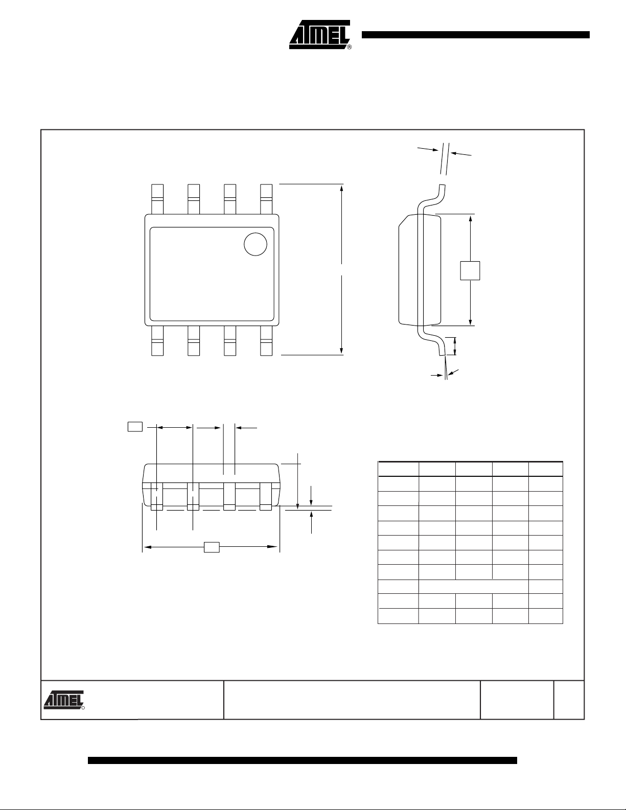
Package Drawing
8S1 – JEDEC SOIC
C
1
E
N
∅
E1
L
Top View
End View
e
D
Side View
B
A
SYMBOL
A1
A 1.35 – 1.75
A1 0.10 – 0.25
b 0.31 – 0.51
C 0.17 – 0.25
D 4.80 – 5.00
E1 3.81 – 3.99
E 5.79 – 6.20
e 1.27 BSC
L 0.40 – 1.27
∅ 0˚ – 8˚
COMMON DIMENSIONS
(Unit of Measure = mm)
MIN
NOM
MAX
NOTE
16
Note:
These drawings are for general information only. Refer to JEDEC Drawing MS-012, Variation AA for proper dimensions, tolerances, datums, etc.
1150 E. Cheyenne Mtn. Blvd.
Colorado Springs, CO 80906
R
TITLE
8S1, 8-lead (0.150" Wide Body), Plastic Gull Wing
Small Outline (JEDEC SOIC)
DRAWING NO.
10/7/03
REV.
8S1 B
3346C–SEEPR–7/04
Page 17
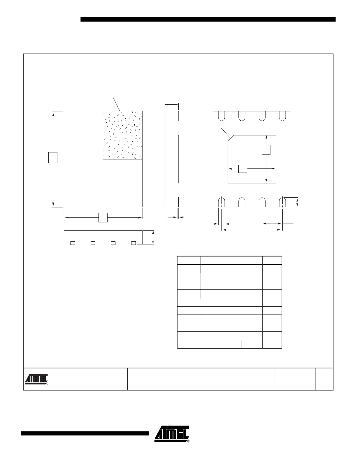
8Y4 – SAP
PIN 1 INDEX AREA
D
E
1150 E. Cheyenne Mtn. Blvd.
R
Colorado Springs, CO 80817
A
PIN 1 ID
E1
A1
b
e1
A
COMMON DIMENSIONS
(Unit of Measure = mm)
SYMBOL
A – – 0.90
A1 0.00 – 0.05
D 5.80 6.00 6.20
E 4.70 4.90 5.10
D1 2.85 3.00 3.15
E1 2.85 3.00 3.15
b 0.35 0.40 0.45
e 1.27 TYP
e1 3.81 REF
L 0.50 0.60 0.70
TITLE
8Y4, 8-lead (6.00 x 4.90 mm Body) SOIC Array Package
(SAP) Y4
MIN
NOM
MAX
D1
NOTE
DRAWING NO.
8Y4
L
e
5/24/04
REV.
A
3346C–SEEPR–7/04
17
Page 18

Atmel Corporation Atmel Operations
2325 Orchard Parkway
San Jose, CA 95131, USA
Tel: 1(408) 441-0311
Fax: 1(408) 487-2600
Regional Headquarters
Europe
Atmel Sarl
Route des Arsenaux 41
Case Postale 80
CH-1705 Fribourg
Switzerland
Tel: (41) 26-426-5555
Fax: (41) 26-426-5500
Asia
Room 1219
Chinachem Golden Plaza
77 Mody Road Tsimshatsui
East Kowloon
Hong Kong
Tel: (852) 2721-9778
Fax: (852) 2722-1369
Japan
9F, Tonetsu Shinkawa Bldg.
1-24-8 Shinkawa
Chuo-ku, Tokyo 104-0033
Japan
Tel: (81) 3-3523-3551
Fax: (81) 3-3523-7581
Memory
2325 Orchard Parkway
San Jose, CA 95131, USA
Tel: 1(408) 441-0311
Fax: 1(408) 436-4314
Microcontrollers
2325 Orchard Parkway
San Jose, CA 95131, USA
Tel: 1(408) 441-0311
Fax: 1(408) 436-4314
La Chantrerie
BP 70602
44306 Nantes Cedex 3, France
Tel: (33) 2-40-18-18-18
Fax: (33) 2-40-18-19-60
ASIC/ASSP/Smart Cards
Zone Industrielle
13106 Rousset Cedex, France
Tel: (33) 4-42-53-60-00
Fax: (33) 4-42-53-60-01
1150 East Cheyenne Mtn. Blvd.
Colorado Springs, CO 80906, USA
Tel: 1(719) 576-3300
Fax: 1(719) 540-1759
Scottish Enterprise Technology Park
Maxwell Building
East Kilbride G75 0QR, Scotland
Tel: (44) 1355-803-000
Fax: (44) 1355-242-743
RF/Automotive
Theresienstrasse 2
Postfach 3535
74025 Heilbronn, Germany
Tel: (49) 71-31-67-0
Fax: (49) 71-31-67-2340
1150 East Cheyenne Mtn. Blvd.
Colorado Springs, CO 80906, USA
Tel: 1(719) 576-3300
Fax: 1(719) 540-1759
Biometrics/Imaging/Hi-Rel MPU/
High Speed Converters/RF Datacom
Avenue de Rochepleine
BP 123
38521 Saint-Egreve Cedex, France
Tel: (33) 4-76-58-30-00
Fax: (33) 4-76-58-34-80
Literature Requests
www.atmel.com/literature
Disclaimer: Atmel Corporation makes no warranty for the use of its products, other than those expressly contained in the Company’s standard
warranty which is detailed in Atmel’s Terms and Conditions located on the Company’s web site. The Company assumes no responsibility for any
errors which may appear in this document, reserves the right to change devices or specifications detailed herein at any time without notice, and
does not make any commitment to update the information contained herein. No licenses to patents or other intellectual property of Atmel are
granted by the Company in connection with the sale of Atmel products, expressly or by implication. Atmel’s products are not authorized for use
as critical components in life support devices or systems.
© Atmel Corporation 2004. All rights reserved. Atmel® and combinations thereof, are the registered
trademarks of Atmel Corporation or its subsidiaries. Other terms and product names may be the trademarks of
others.
Printed on recycled paper.
3346C–SEEPR–7/04
 Loading...