

Page 1

AT25DQ321
32-Mbit, 2.7V Minimum SPI Serial Flash Memory
with Dual-I/O and Quad-I/O Support
DATASHEET
Features
Single 2.7V - 3.6V supply
Serial Peripheral Interface (SPI) compatible
Supports SPI Modes 0 and 3
Supports RapidS
Supports Dual- and Quad-Input Program
Supports Dual- and Quad-Output Read
Very high operating frequencies
100MHz for RapidS
85MHz for SPI
Clock-to-output (t
Flexible, optimized erase architecture for code + data storage applications
Uniform 4KB, 32KB, and 64KB Block Erase
Full Chip Erase
Individual sector protection with Global Protect/Unprotect feature
64 sectors of 64KB each
Hardware controlled locking of protected sectors via WP pin
Sector Lockdown
Make any combination of 64KB sectors permanently read-only
128-byte Programmable OTP Security Register
Flexible programming
Byte/Page Program (1 to 256 bytes)
Fast Program and Erase times
1.5ms typical Page Program (256 bytes) time
50ms typical 4KB Block Erase time
250ms typical 32KB Block Erase time
400ms typical 64KB Block Erase time
Program and Erase Suspend/Resume
Automatic checking and reporting of erase/program failures
Software controlled reset
JEDEC Standard Manufacturer and Device ID Read Methodology
Low power dissipation
7mA Active Read current (typical at 20MHz)
5μA Deep Power-Down current (typical)
Endurance: 100,000 program/erase cycles
Data retention: 20 years
Complies with full industrial temperature range
Industry standard green (Pb/Halide-free/RoHS compliant) package options
8-lead SOIC (208-mil wide)
8-pad Ultra-thin DFN (5 x 6 x 0.6mm)
16-lead SOIC (300-mil wide)
™
operation
) of 5ns maximum
V
8718D–DFLASH–12/2012
Page 2

1. Description
The AT25DQ321 is a serial interface Flash memory device designed for use in a wide variety of high-volume consumer
based applications in which program code is shadowed from Flash memory into embedded or external RAM for
execution. The flexible erase architecture of the AT25DQ321, with its erase granularity as small as 4KB, makes it ideal
for data storage as well, eliminating the need for additional data storage EEPROM devices.
The physical sectoring and the erase block sizes of the AT25DQ321 have been optimized to meet the needs of today's
code and data storage applications. By optimizing the size of the physical sectors and erase blocks, the memory space
can be used much more efficiently. Because certain code modules and data storage segments must reside by
themselves in their own protected sectors, the wasted and unused memory space that occurs with large sectored and
large block erase Flash memory devices can be greatly reduced. This increased memory space efficiency allows
additional code routines and data storage segments to be added while still maintaining the same overall device density.
The AT25DQ321 also offers a sophisticated method for protecting individual sectors against erroneous or malicious
program and erase operations. By providing the ability to individually protect and unprotect sectors, a system can
unprotect a specific sector to modify its contents while keeping the remaining sectors of the memory array securely
protected. This is useful in applications where program code is patched or updated on a subroutine or module basis, or in
applications where data storage segments need to be modified without running the risk of errant modifications to the
program code segments. In addition to individual sector protection capabilities, the AT25DQ321 incorporates Global
Protect and Global Unprotect features that allow the entire memory array to be either protected or unprotected all at
once. This reduces overhead during the manufacturing process since sectors do not have to be unprotected one-by-one
prior to initial programming.
To take code and data protection to the next level, the AT25DQ321 incorporates a sector lockdown mechanism that
allows any combination of individual 64KB sectors to be locked down and become permanently read-only. This
addresses the need of certain secure applications that require portions of the Flash memory array to be permanently
protected against malicious attempts at altering program code, data modules, security information or
encryption/decryption algorithms, keys, and routines. The device also contains a specialized OTP (One-Time
Programmable) Security Register that can be used for purposes such as unique device serialization, system-level
Electronic Serial Number (ESN) storage, locked key storage, etc.
Specifically designed for use in 3V systems, the AT25DQ321 supports read, program, and erase operations with a
supply voltage range of 2.7V to 3.6V. No separate voltage is required for programming and erasing.
AT25DQ321 [DATASHEET]
8718D–DFLASH–12/2012
2
Page 3

2. Pin Descriptions and Pinouts
Table 2-1. Pin Descriptions
Symbol Name and Function
Chip Select: Asserting the CS pin selects the device. When the CS pin is
deasserted, the device will be deselected and normally be placed in standby
mode (not Deep Power-Down mode) and the SO pin will be in a
high-impedance state. When the device is deselected, data will not be
CS
SCK
SI (I/O0)
accepted on the SI pin.
A high-to-low transition on the
low-to-high transition is required to end an operation. When ending an internally
self-timed operation such as a program or erase cycle, the device will not enter
the standby mode until the completion of the operation.
Serial Clock: This pin is used to provide a clock to the device and is used to
control the flow of data to and from the device. Command, address and input
data present on the SI pin or I/O pins is always latched in on the rising edge of
SCK, while output data on the SO pin or I/O pins is always clocked out on the
falling edge of SCK.
Serial Input (I/O0): The SI pin is used to shift data into the device. The SI pin is
used for all data input including command and address sequences. Data on the
SI pin is always latched in on the rising edge of SCK.
With the Dual-Input and Quad-Input Byte/Page Program commands, the SI pin
is used as an input pin (I/O
(on I/O
) or four bits (on I/O
1-0
) in conjunction with other pins to allow two bits
0
3-0
SCK. With the Dual-Output and Quad-Output Read Array commands, the SI
pin becomes an output pin (I/O
(on I/O
) or four bits (on I/O
1-0
3-0
of SCK. To maintain consistency with SPI nomenclature, the SI (I/O
referenced as SI throughout the document with exception to sections dealing
with the Dual-Input and Quad-Dual-Output Byte/Page Program commands as
well as the Dual-Output and Quad-Output Read Array commands in which it will
be referenced as I/O
.
0
Data present on the SI pin will be ignored whenever the device is deselected
CS is deasserted).
(
CS pin is required to start an operation and a
) of data to be clocked in on every rising edge of
) and, along with other pins, allows two bits
0
) of data to be clocked out on every falling edge
) pin will be
0
Asserted
State
Low Input
- Input
- Input/Output
Type
SO (I/O1)
Serial Output (I/O1): The SO pin is used to shift data out from the device. Data
on the SO pin is always clocked out on the falling edge of SCK.
With the Dual-Input and Quad-Input Byte/Page Program commands, the SO pin
becomes an input pin (I/O
(on I/O
) or four bits (on I/O
1-0
) and, along with other pins, allows two bits
1
) of data to be clocked in on every rising edge of
3-0
SCK. With the Dual-Output and Quad-Output Read Array commands, the SO
pin is used as an output pin (I/O
(on I/O
) or four bits (on I/O
1-0
of SCK. To maintain consistency with SPI nomenclature, the SO (I/O
) in conjunction with other pins to allow two bits
1
) of data to be clocked out on every falling edge
3-0
) pin will
1
be referenced as SO throughout the document with exception to sections
dealing with the Dual-Input and Quad-Input Byte/Page Program commands as
well as the Dual-Output and Quad-Output Read Array commands in which it will
be referenced as I/O
.
1
The SO pin will be in a high-impedance state whenever the device is deselected
CS is deasserted).
(
AT25DQ321 [DATASHEET]
- Input/Output
3
8718D–DFLASH–12/2012
Page 4
Table 2-1. Pin Descriptions (Continued)
Symbol Name and Function
Write Protect (I/O2): The WP# pin controls the hardware locking feature of the
device. See “Protection Commands and Features” on page 24 for more details
on protection features and the
With the Quad-Input Byte/Page Program command, the
WP (I/O2)
input pin (I/O
be clocked in on every rising edge of SCK. With the Quad-Output Read Array
command, the
) and, along with other pins, allows four bits (on I/O
2
WP pin becomes an output pin (I/O2) and, when used with other
pins, allows four bits (on I/O
SCK. The QE bit in the Configuration Register must be set in order for the
pin to be used as an I/O data pin.
WP pin must be driven at all times or pulled-high using an external pull-up
The
resistor.
Hold (I/O3): The HOLD pin is used to temporarily pause serial communication
without deselecting or resetting the device. While the
transitions on the SCK pin and data on the SI pin will be ignored and the SO pin
will be in a high-impedance state.
The
CS pin must be asserted and the SCK pin must be in the low state in order
for a Hold condition to start. A Hold condition pauses serial communication only
and does not have an affect on internally self-timed operations such as a
program or erase cycle. See “Hold” on page 53 for additional details on the Hold
HOLD (I/O3)
operation.
With the Quad-Input Byte/Page Program command, the
input pin (I/O
) and, along with other pins, allows four bits (on I/O
3
be clocked in on every rising edge of SCK. With the Quad-Output Read Array
command, the
HOLD pin becomes an output pin (I/O3) and, when used with
other pins, allows four bits (on I/O
edge of SCK. The QE bit in the Configuration Register must be set in order for
the
HOLD pin to be used as an I/O data pin.
HOLD pin must be driven at all times or pulled-high using an external
The
pull-up resistor.
WP pin.
WP pin becomes an
) of data to
3-0
) of data to be clocked out on every falling edge of
3-0
HOLD pin is asserted,
HOLD pin becomes an
) of data to
3-0
) of data to be clocked out on every falling
3-0
WP
Asserted
State
Type
Low Input/Output
Low Input/Output
Device Power Supply: The VCC pin is used to supply the source voltage to the
V
CC
device.
Operations at invalid V
be attempted.
GND
Ground: The ground reference for the power supply. GND should be
connected to the system ground.
Figure 2-1. Pin Configurations
8-lead SOIC
CS
SO (I/O
WP (I/O2)
GND
1
)
2
1
3
4
8
7
6
5
V
CC
HOLD (I/O3)
SCK
SI (I/O0)
voltages may produce spurious results and should not
CC
CS
SO (I/O1)
WP (I/O2)
GND
8-pad UDFN
8
1
7
2
6
3
5
4
V
CC
HOLD (I/O3)
SCK
SI (I/O0)
NC
V
NC
NC
NC
NC
CS
SO
CC
16-lead SOIC
1
2
3
4
5
6
7
8
AT25DQ321 [DATASHEET]
- Power
- Power
SCK
16
SI
15
NC
14
NC
13
NC
12
NC
11
GND
10
WP
9
8718D–DFLASH–12/2012
4
Page 5
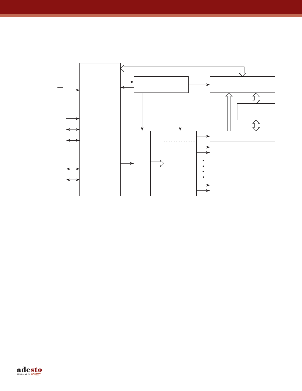
3. Block Diagram
Figure 3-1. Block Diagram
SI (I/O0)
SO (I/O1)
WP (I/O2)
HOLD (I/O3)
Note: I/O
Control and
CS
SCK
pin naming convention is used for Dual-I/O and Quad-I/O commands.
3-0
Interface
Control
And
Logic
Protection Logic
Y-Decoder
X-Decoder
Address Latch
I/O Buffers
and Latches
SRAM
Data Buffer
Y-Gating
Flash
Memory
Array
AT25DQ321 [DATASHEET]
8718D–DFLASH–12/2012
5
Page 6
4. Memory Array
–
–
–
–
–
–
–
–
–
–
–
–
–
–
–
–
–
–
–
–
–
–
–
–
–
–
–
–
–
–
–
–
–
–
–
–
–
–
–
–
–
–
–
–
–
–
–
–
–
–
–
To provide the greatest flexibility, the memory array of the AT25DQ321 can be erased in four levels of granularity
including a Full Chip Erase. In addition, the array has been divided into physical sectors of uniform size, of which each
sector can be individually protected from program and erase operations. The size of the physical sectors is optimized for
both code and data storage applications, allowing both code and data segments to reside in their own isolated regions.
The Memory Architecture Diagram illustrates the breakdown of each erase level as well as the breakdown of each
physical sector.
Figure 4-1. Memory Architecture Diagram
Block Erase Detail Page Program Detail
Internal Sectoring for 64KB 32KB 4KB 1-256 Byte
Sector Protection Block Erase Block Erase Block Erase Page Program
Function (D8h Command) (52h Command) (20h Command) (02h Command)
3FF000h 256 bytes 3FFFFFh–3FFF00h
3FE000h 256 bytes 3FFEFFh–3FFE00h
3FD000h 256 bytes 3FFDFFh–3FFD00h
3FC000h 256 bytes 3FFCFFh–3FFC00h
3FB000h 256 bytes 3FFBFFh–3FFB00h
3FA000h 256 bytes 3FFAFFh–3FFA00h
3F9000h 256 bytes 3FF9FFh–3FF900h
3F8000h 256 bytes 3FF8FFh–3FF800h
3F7000h 256 bytes 3FF7FFh–3FF700h
3F6000h 256 bytes 3FF6FFh–3FF600h
3F5000h 256 bytes 3FF5FFh–3FF500h
3F4000h 256 bytes 3FF4FFh–3FF400h
3F3000h 256 bytes 3FF3FFh–3FF300h
3F2000h 256 bytes 3FF2FFh–3FF200h
3F1000h 256 bytes 3FF1FFh–3FF100h
3F0000h 256 bytes 3FF0FFh–3FF000h
3EF000h 256 bytes 3FEFFFh–3FEF00h
3EE000h 256 bytes 3FEEFFh–3FEE00h
3ED000h 256 bytes 3FEDFFh–3FED00h
3EC000h 256 bytes 3FECFFh–3FEC00h
3EB000h 256 bytes 3FEBFFh–3FEB00h
3EA000h 256 bytes 3FEAFFh–3FEA00h
3E9000h 256 bytes 3FE9FFh–3FE900h
3E8000h 256 bytes 3FE8FFh–3FE800h
3E7000h
3E6000h
3E5000h
3E4000h 256 bytes 0017FFh–001700h
3E3000h 256 bytes 0016FFh–001600h
3E2000h 256 bytes 0015FFh–001500h
3E1000h 256 bytes 0014FFh–001400h
3E0000h 256 bytes 0013FFh–001300h
00F000h 256 bytes 000FFFh–000F00h
00E000h 256 bytes 000EFFh–000E00h
00D000h 256 bytes 000DFFh–000D00h
00C000h 256 bytes 000CFFh–000C00h
00B000h 256 bytes 000BFFh–000B00h
00A000h 256 bytes 000AFFh–000A00h
009000h 256 bytes 0009FFh–000900h
008000h 256 bytes 0008FFh–000800h
007000h 256 bytes 0007FFh–000700h
006000h 256 bytes 0006FFh–000600h
005000h 256 bytes 0005FFh–000500h
004000h 256 bytes 0004FFh–000400h
003000h 256 bytes 0003FFh–000300h
002000h 256 bytes 0002FFh–000200h
001000h 256 bytes 0001FFh–000100h
000000h 256 bytes 0000FFh–000000h
•
•
•
256 bytes 0012FFh
256 bytes 0011FFh
256 bytes 0010FFh
64KB
(Sector 63)
64KB
(Sector 62)
•
•
•
64KB
(Sector 0)
64KB
64KB
64KB
4KB
4KB
4KB
32KB
32KB
32KB
32KB
•
•
•
• • •
32KB
32KB
4KB
4KB
4KB
4KB
4KB
4KB
4KB
4KB
4KB
4KB
4KB
4KB
4KB
4KB
4KB
4KB
4KB
4KB
4KB
4KB
4KB
4KB
4KB
4KB
4KB
4KB
4KB
4KB
4KB
• • •
4KB
4KB
4KB
4KB
4KB
4KB
4KB
4KB
4KB
4KB
4KB
4KB
4KB
4KB
4KB
4KB
3FFFFFh
3FEFFFh
3FDFFFh
3FCFFFh
3FBFFFh
3FAFFFh
3F9FFFh
3F8FFFh
3F7FFFh
3F6FFFh
3F5FFFh
3F4FFFh
3F3FFFh
3F2FFFh
3F1FFFh
3F0FFFh
3EFFFFh
3EEFFFh
3EDFFFh
3ECFFFh
3EBFFFh
3EAFFFh
3E9FFFh
3E8FFFh
3E7FFFh
3E6FFFh
3E5FFFh
3E4FFFh
3E3FFFh
3E2FFFh
3E1FFFh
3E0FFFh
00FFFFh
00EFFFh
00DFFFh
00CFFFh
00BFFFh
00AFFFh
009FFFh
008FFFh
007FFFh
006FFFh
005FFFh
004FFFh
003FFFh
002FFFh
001FFFh
000FFFh
Page AddressBlock Address
RangeRange
001200h
001100h
001000h
AT25DQ321 [DATASHEET]
8718D–DFLASH–12/2012
6
Page 7
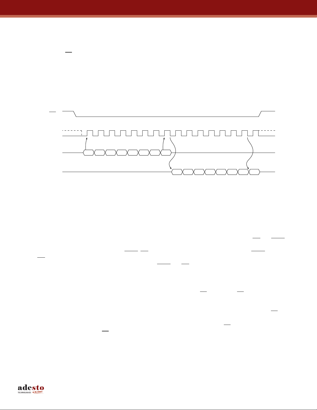
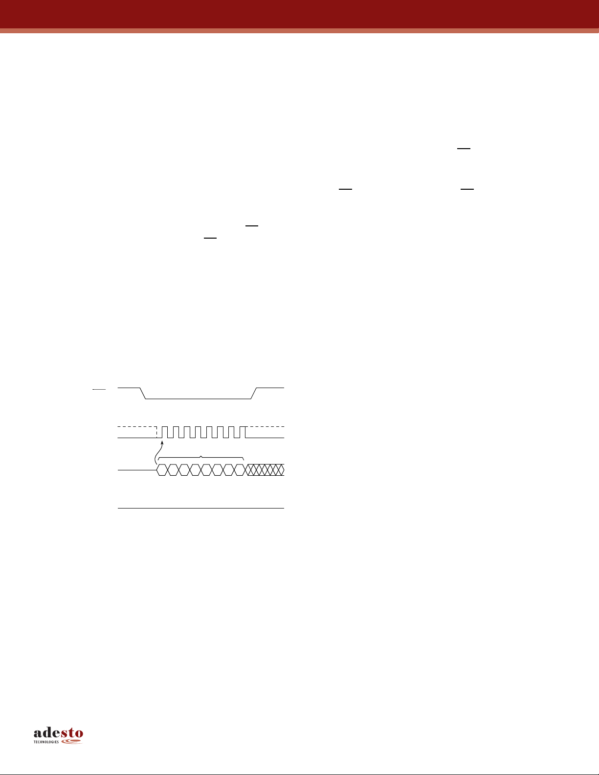
5. Device Operation
The AT25DQ321 is controlled by a set of instructions that are sent from a host controller, commonly referred to as the SPI
Master. The SPI Master communicates with the AT25DQ321 via the SPI bus which is comprised of four signal lines:
Chip Select (
The SPI protocol defines a total of four modes of operation (mode 0, 1, 2, or 3) with each mode differing in respect to the
SCK polarity and phase and how the polarity and phase control the flow of data on the SPI bus. The AT25DQ321 supports
the two most common modes, SPI Modes 0 and 3. The only difference between SPI Modes 0 and 3 is the polarity of the
SCK signal when in the inactive state (when the SPI Master is in standby mode and not transferring any data). With SPI
Modes 0 and 3, data is always latched in on the rising edge of SCK and always output on the falling edge of SCK.
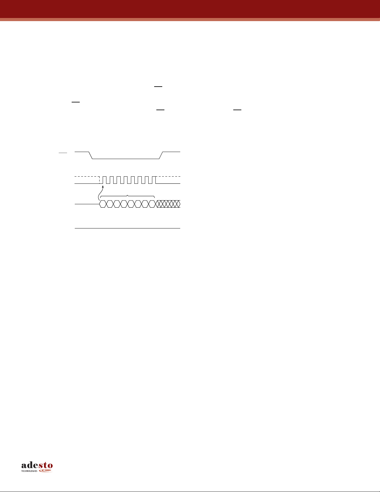
Figure 5-1. SPI Mode 0 and 3
CS
SCK
CS), Serial Clock (SCK), Serial Input (SI), and Serial Output (SO).
SI
SO
MSB LSB
5.1 Dual-I/O and Quad-I/O Operation
The AT25DQ321 features a Dual-Input Program mode and a Dual-Output Read mode that allows two bits of data to be
clocked into or out of the device every clock cycle to improve throughputs. To accomplish this, both the SI and SO pins
are utilized as inputs/outputs for the transfer of data bytes. With the Dual-Input Byte/Page Program command, the the SO
pin becomes an input along with the SI pin. Alternatively, with the Dual-Output Read Array command, the SI pin becomes
an output along with the SO pin. For both Dual-I/O commands, the SO pin will be referred to as I/O
referred to as I/O
.
0
The device also supports a Quad-Input Program mode and a Quad-Output Read mode in which the
become data pins for even higher throughputs. For the Quad-Input Byte/Page Program command and for the
Quad-Output Read Array command, the
HOLD, WP, SO, and SI pins are referred to as I/O
WP becomes I/O2, SO becomes I/O1, and SI becomes I/O0. The QE bit in the Configuration Register must be set in order
for both Quad-I/O commands to be enabled and for the
6. Commands and Addressing
A valid instruction or operation must always be started by first asserting the CS pin. After the CS pin has been asserted,
the host controller must then clock out a valid 8-bit opcode on the SPI bus. Following the opcode, instruction dependent
information such as address and data bytes would then be clocked out by the host controller. All opcode, address, and
data bytes are transferred with the Most-Significant Bit (MSB) first. An operation is ended by deasserting the
Opcodes not supported by the AT25DQ321 will be ignored by the device and no operation will be started. The device will
continue to ignore any data presented on the SI pin until the start of the next operation (
reasserted). In addition, if the
then no operation will be performed and the device will simply return to the idle state and wait for the next operation.
Addressing of the device requires a total of three bytes of information to be sent, representing address bits A23-A0. Since
the upper address limit of the AT25DQ321 memory array is 3FFFFFh, address bits A23-A22 are always ignored by the
device.
CS pin is deasserted before complete opcode and address information is sent to the device,
MSB LSB
and the SI pin will be
1
WP and HOLD pins
where HOLD becomes I/O3,
3-0
HOLD and WP pins to be converted to I/O data pins.
CS pin being deasserted and then
CS pin.
AT25DQ321 [DATASHEET]
8718D–DFLASH–12/2012
7
Page 8

Table 6-1. Command Listing
Command Opcode
Clock
Frequency
Address
Bytes
Dummy
Bytes
Read Commands
1Bh 0001 1011 Up to 100MHz 3 2 1+
Read Array
0Bh 0000 1011 Up to 85MHz 3 1 1+
03h 0000 0011 Up to 50MHz 3 0 1+
Dual-Output Read Array 3Bh 0011 1011 Up to 85MHz 3 1 1+
Quad-Output Read Array 6Bh 0110 1011 Up to 66MHz 3 1 1+
Program and Erase Commands
Block Erase (4KB) 20h 0010 0000 Up to 100MHz 3 0 0
Block Erase (32KB) 52h 0101 0010 Up to 100MHz 3 0 0
Block Erase (64KB) D8h 1101 1000 Up to 100MHz 3 0 0
Chip Erase
60h 0110 0000 Up to 100MHz 0 0 0
C7h 1100 0111 Up to 100MHz 0 0 0
Byte/Page Program (1 to 256 bytes) 02h 0000 0010 Up to 100MHz 3 0 1+
Dual-Input Byte/Page Program (1 to 256 bytes) A2h 1010 0010 Up to 100MHz 3 0 1+
Quad-Input Byte/Page Program (1 to 256 bytes) 32h 0011 0010 Up to 100MHz 3 0 1+
Program/Erase Suspend B0h 1011 0000 Up to 100MHz 0 0 0
Program/Erase Resume D0h 1101 0000 Up to 100MHz 0 0 0
Protection Commands
Write Enable 06h 0000 0110 Up to 100MHz 0 0 0
Write Disable 04h 0000 0100 Up to 100MHz 0 0 0
Protect Sector 36h 0011 0110 Up to 100MHz 3 0 0
Unprotect Sector 39h 0011 1001 Up to 100MHz 3 0 0
Global Protect/Unprotect Use Write Status Register Byte 1 Command
Read Sector Protection Registers 3Ch 0011 1100 Up to 100MHz 3 0 1+
Security Commands
Sector Lockdown 33h 0011 0011 Up to 100MHz 3 0 1
Freeze Sector Lockdown State 34h 0011 0100 Up to 100MHz 3 0 1
Read Sector Lockdown Registers 35h 0011 0101 Up to 100MHz 3 0 1+
Program OTP Security Register 9Bh 1001 1011 Up to 100MHz 3 0 1+
Read OTP Security Register 77h 0111 0111 Up to 100MHz 3 2 1+
Status and Configuration Register Commands
Read Status Register 05h 0000 0101 Up to 100MHz 0 0 1+
Write Status Register Byte 1 01h 0000 0001 Up to 100MHz 0 0 1
Write Status Register Byte 2 31h 0011 0001 Up to 100MHz 0 0 1
Read Configuration Register 3Fh 0011 1111 Up to 100MHz 0 0 1+
Write Configuration Register 3Eh 0011 1110 Up to 100MHz 0 0 1
Miscellaneous Commands
Reset F0h 1111 0000 Up to 100MHz 0 0 1
Read Manufacturer and Device ID 9Fh 1001 1111 Up to 85MHz 0 0 1 to 4
Deep Power-Down B9h 1011 1001 Up to 100MHz 0 0 0
Resume from Deep Power-Down ABh 1010 1011 Up to 100MHz 0 0 0
Data
Bytes
AT25DQ321 [DATASHEET]
8718D–DFLASH–12/2012
8
Page 9
7. Read Commands
7.1 Read Array
The Read Array command can be used to sequentially read a continuous stream of data from the device by simply
providing the clock signal once the initial starting address has been specified. The device incorporates an internal
address counter that automatically increments on every clock cycle.
Three opcodes (1Bh, 0Bh, and 03h) can be used for the Read Array command. The use of each opcode depends on the
maximum clock frequency that will be used to read data from the device. The 0Bh opcode can be used at any clock
frequency up to the maximum specified by f
to the maximum specified by f
any clock frequency up to the maximum specified by f
should be reserved to systems employing the RapidS protocol.
f
CLK
To perform the Read Array operation, the
must be clocked into the device. After the opcode has been clocked in, the three address bytes must be clocked in to
specify the starting address location of the first byte to read within the memory array. Following the three address bytes,
additional dummy bytes may need to be clocked into the device depending on which opcode is used for the Read Array
operation. If the 1Bh opcode is used, then two dummy bytes must be clocked into the device after the three address
bytes. If the 0Bh opcode is used, then a single dummy byte must be clocked in after the address bytes.
After the three address bytes (and the dummy bytes or byte if using opcodes 1Bh or 0Bh) have been clocked in,
additional clock cycles will result in data being output on the SO pin. The data is always output with the MSB of a byte
first. When the last byte (3FFFFFh) of the memory array has been read, the device will continue reading back at the
beginning of the array (000000h). No delays will be incurred when wrapping around from the end of the array to the
beginning of the array.
Deasserting the
be deasserted at any time and does not require that a full byte of data be read.
CS pin will terminate the read operation and put the SO pin into a high-impedance state. The CS pin can
, and the 03h opcode can be used for lower frequency read operations up
CLK
. The 1Bh opcode allows the highest read performance possible and can be used at
RDLF
; however, use of the 1Bh opcode at clock frequencies above
MAX
CS pin must first be asserted and the appropriate opcode (1Bh, 0Bh, or 03h)
Figure 7-1. Read Array – 1Bh Opcode
CS
2310
675410119812 394243414037 3833 36353431 3229 30 44 47 484645 50 5149 52 55 565453
SCK
Opcode
SI
SO
00011011
MSB MSB
High-impedance
AAAA AAAAA
Address Bits A23-A0
Don't Care
XXXXXXXX
MSB
Don't Care
XXXXXXXX
MSB
Data Byte 1
DDDDDDDDDD
MSB MSB
AT25DQ321 [DATASHEET]
8718D–DFLASH–12/2012
9
Page 10
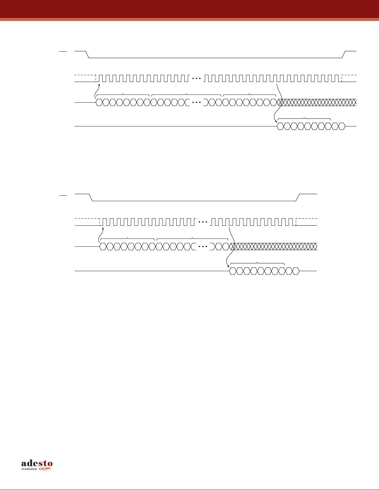
Figure 7-2. Read Array – 0Bh Opcode
CS
2310
SCK
Opcode
SI
SO
00001011
MSB MSB
High-impedance
Figure 7-3. Read Array – 03h Opcode
CS
2310
SCK
Opcode
SI
SO
00000011
MSB MSB
High-impedance
675410119812 394243414037 3833 36353431 3229 30 44 47 484645
Address Bits A23-A0 Don't Care
AAAA AAAAA
675410119812 373833 36353431 3229 30 39 40
Address Bits A23-A0
AAAA AAAAA
XXXXXXXX
MSB
Data Byte 1
DDDDDDDDDD
MSB MSB
Data Byte 1
DDDDDDDDDD
MSB MSB
AT25DQ321 [DATASHEET]
8718D–DFLASH–12/2012
10
Page 11
7.2 Dual-Output Read Array
The Dual-Output Read Array command is similar to the standard Read Array command and can be used to sequentially
read a continuous stream of data from the device by simply providing the clock signal once the initial starting address has
been specified. Unlike the standard Read Array command however, the Dual-Output Read Array command allows two
bits of data to be clocked out of the device on every clock cycle rather than just one.
The Dual-Output Read Array command can be used at any clock frequency up to the maximum specified by f
perform the Dual-Output Read Array operation, the
into the device. After the opcode has been clocked in, the three address bytes must be clocked in to specify the starting
address location of the first byte to read within the memory array. Following the three address bytes, a single dummy
byte must also be clocked into the device.
After the three address bytes and the dummy byte have been clocked in, additional clock cycles will result in data being
output on both the I/O1 and I/O0 pins. The data is always output with the MSB of a byte first, and the MSB is always
output on the I/O
same data byte will be output on the I/O
on the I/O
1
cycles. When the last byte (3FFFFFh) of the memory array has been read, the device will continue reading back at the
beginning of the array (000000h). No delays will be incurred when wrapping around from the end of the array to the
beginning of the array.
Deasserting the
can be deasserted at any time and does not require that a full byte of data be read.
Figure 7-4. Dual-Output Read Array
pin. During the first clock cycle, bit 7 of the first data byte will be output on the I/O1 pin while bit 6 of the
1
and I/O0 pins, respectively. The sequence continues with each byte of data being output after every four clock
CS pin will terminate the read operation and put the I/O
. To
RDDO
CS pin must first be asserted and the opcode of 3Bh must be clocked
pin. During the next clock cycle, bits 5 and 4 of the first data byte will be output
0
pins into a high-impedance state. The CS pin
1-0
CS
SCK
SI (I/O
SO (I/O1)
2310
Opcode
)
0
00111011
MSB MSB
High-impedance
675410119812 394243414037 3833 36353431 3229 30 44 47 484645
Address Bits A23-A0 Don't Care
AAAA AAAAA
XXXXXXXX
MSB
Output
Data Byte 1
D6 D4 D2 D0 D6 D4 D2 D0 D6 D
D7 D5 D3 D1 D7 D5 D3 D1 D7 D
MSB MSB
Output
Data Byte 2
4
5
AT25DQ321 [DATASHEET]
8718D–DFLASH–12/2012
11
Page 12
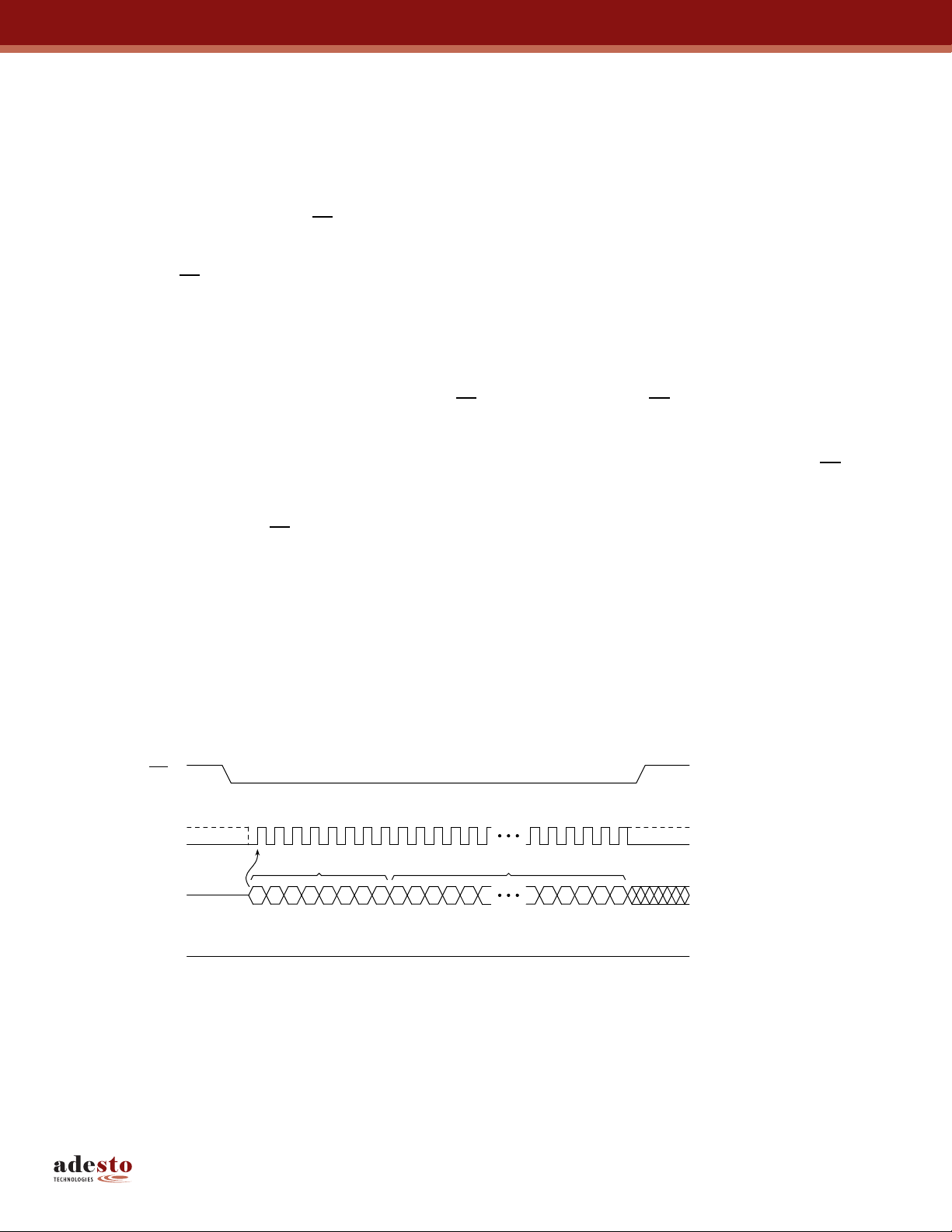
7.3 Quad-Output Read Array
The Quad-Output Read Array command is similar to the Dual-Output Read Array command and can be used to
sequentially read a continuous stream of data from the device by simply providing the clock signal once the initial starting
address has been specified. Unlike the Dual-Output Read Array command however, the Quad-Output Read Array
command allows four bits of data to be clocked out of the device on every clock cycle rather than two.
The Quad-Output Read Array command can be used at any clock frequency up to the maximum specified by f
perform the Quad-Output Read Array operation, the
clocked into the device. After the opcode has been clocked in, the three address bytes must be clocked in to specify the
starting address location of the first byte to read within the memory array. Following the three address bytes, a single
dummy byte must also be clocked into the device.
After the three address bytes and the dummy byte have been clocked in, additional clock cycles will result in data being
output on the I/O
pin. During the first clock cycle, bit 7 of the first data byte will be output on the I/O
data byte will be output on the I/O
first data byte will be output on the I/O
data being output after every two clock cycles. When the last byte (3FFFFFh) of the memory array has been read, the
device will continue reading back at the beginning of the array (000000h). No delays will be incurred when wrapping
around from the end of the array to the beginning of the array.
Deasserting the
can be deasserted at any time and does not require that a full byte of data be read.
Figure 7-5. Quad-Output Read Array
pins. The data is always output with the MSB of a byte first and the MSB is always output on the I/O3
3-0
CS pin will terminate the read operation and put the I/O
. To
RDQO
CS pin must first be asserted and the opcode of 6Bh must be
pin while bits 6, 5, and 4 of the same
3
, I/O1, and I/O0 pins, respectively. During the next clock cycle, bits 3, 2, 1, and 0 of the
2
, I/O2, I/O1 and I/O0 pins, respectively. The sequence continues with each byte of
3
pins into a high-impedance state. The CS pin
3-0
CS
SCK
I/O
(SI)
I/O
(SO)
I/O
(WP)
I/O
(HOLD)
2310
Opcode
0
1
2
3
01101011
06% 06%
High-impedance
High-impedance
High-impedance
675410119812 394243414037 3833 36353431 3229 30 44 47 484645
Byte 1
Byte 2
Address Bits A23-A0 Don't Care
AAAA AAAAA
XXXXXXXX
06%
OUT
D4 D0 D4 D0 D4 D0 D4 D0 D4 D
D5 D1 D5 D1 D5 D1 D5 D1 D5 D
D6 D2 D6 D2 D6 D2 D6 D2 D6 D
D7 D3 D7 D3 D7 D3 D7 D3 D7 D
MSB MSB MSB MSB MSB
OUT
Byte 3
OUT
Byte 4
OUT
Byte 5
OUT
0
1
2
3
AT25DQ321 [DATASHEET]
8718D–DFLASH–12/2012
12
Page 13

8. Program and Erase Commands
8.1 Byte/Page Program
The Byte/Page Program command allows anywhere from a single byte of data to 256 bytes of data to be programmed
into previously erased memory locations. An erased memory location is one that has all eight bits set to the Logical 1
state (a byte value of FFh). Before a Byte/Page Program command can be started, the Write Enable command must
have been previously issued to the device (see “Write Enable” on page 24) to set the Write Enable Latch (WEL) bit of the
Status Register to a Logical 1 state.
To perform a Byte/Page Program command, an opcode of 02h must be clocked into the device followed by the three
address bytes denoting the first byte location of the memory array to begin programming at. After the address bytes have
been clocked in, data can then be clocked into the device and will be stored in an internal buffer.
If the starting memory address denoted by A23-A0 does not fall on an even 256-byte page boundary (A7-A0 are not
all 0), then special circumstances regarding which memory locations to be programmed will apply. In this situation, any
data that is sent to the device that goes beyond the end of the page will wrap around back to the beginning of the same
page.
Example: If the starting address denoted by A23-A0 is 0000FEh and three bytes of data are sent to the device, then
the first two bytes of data will be programmed at addresses 0000FEh and 0000FFh while the last byte of
data will be programmed at address 000000h. The remaining bytes in the page (addresses 000001h
through 0000FDh) will not be programmed and will remain in the erased state (FFh). In addition, if more
than 256 bytes of data are sent to the device, then only the last 256 bytes sent will be latched into the
internal buffer.
When the
CS pin is deasserted, the device will take the data stored in the internal buffer and program it into the
appropriate memory array locations based on the starting address specified by A23-A0 and the number of data bytes
sent to the device. If less than 256 bytes of data were sent to the device, then the remaining bytes within the page will not
be programmed and will remain in the erased state (FFh). The programming of the data bytes is internally self-timed and
should take place in a time of t
The three address bytes and at least one complete byte of data must be clocked into the device before the
deasserted, and the
CS pin must be deasserted on even byte boundaries (multiples of eight bits); otherwise, the device
or tBP if only programming a single byte.
PP
CS pin is
will abort the operation and no data will be programmed into the memory array. In addition, if the address specified by
A23-A0 points to a memory location within a sector that is in the protected state (see “Protect Sector” on page 26) or
locked down (see “Sector Lockdown” on page 32), then the Byte/Page Program command will not be executed and the
device will return to the idle state once the
CS pin has been deasserted. The WEL bit in the Status Register will be reset
back to the Logical 0 state if the program cycle aborts due to an incomplete address being sent, an incomplete byte of
data being sent, the
CS pin being deasserted on non-byte boundaries, or because the memory location to be
programmed is protected or locked down.
While the device is programming, the Status Register can be read and will indicate that the device is busy. For faster
throughput, it is recommended that the Status Register be polled rather than waiting the t
or tPP time to determine if the
BP
data bytes have finished programming. At some point before the program cycle completes, the WEL bit in the Status
Register will be reset back to the Logical 0 state.
The device also incorporates an intelligent programming algorithm that can detect when a byte location fails to program
properly. If a programming error arises, it will be indicated by the EPE bit in the Status Register.
AT25DQ321 [DATASHEET]
8718D–DFLASH–12/2012
13
Page 14
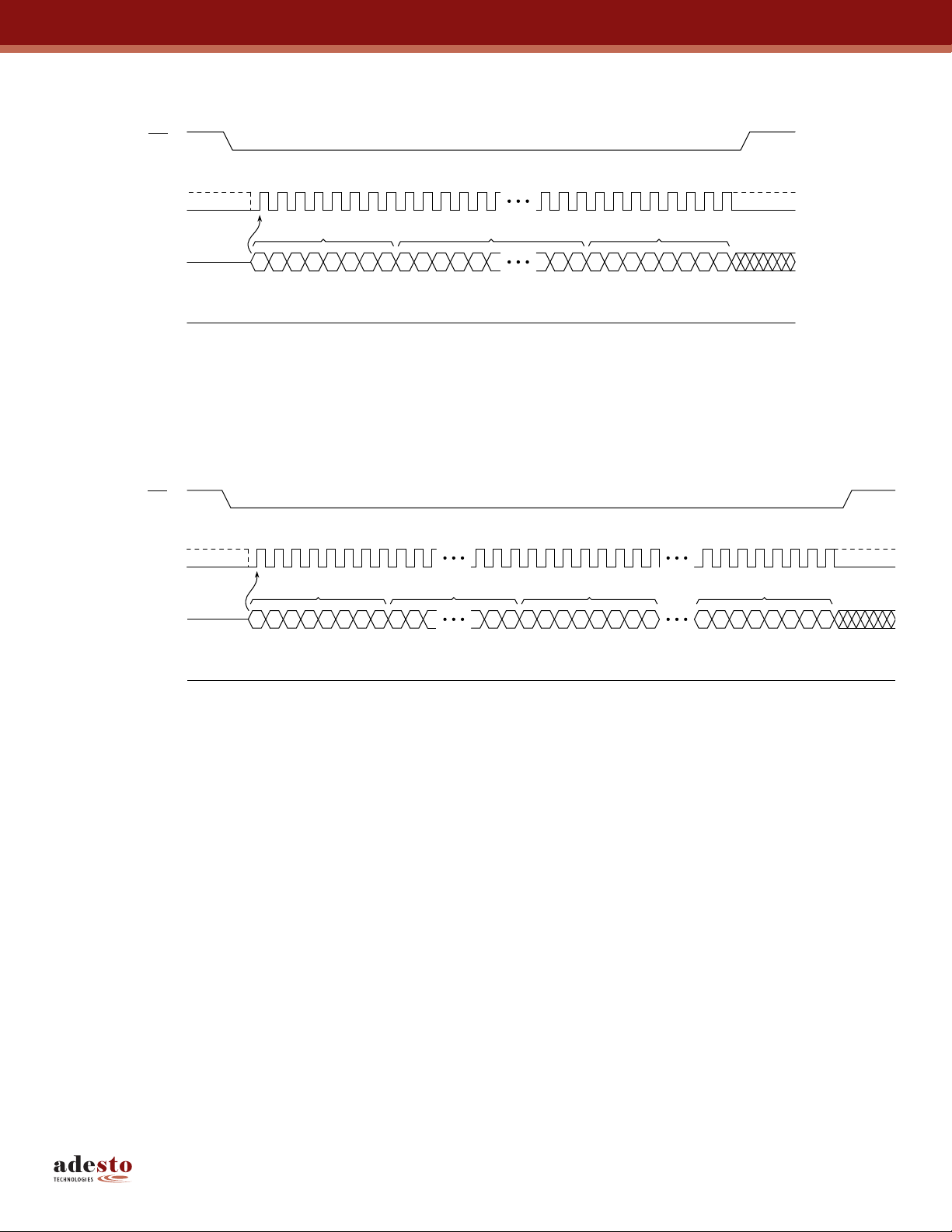
Figure 8-1. Byte Program
CS
SCK
SI
SO
00000010
MSB MSB
High-impedance
Figure 8-2. Page Program
CS
SCK
SI
00000010
MSB MSB
2310
Opcode
2310
Opcode
675410119812 3937 3833 36353431 3229 30
Address Bits A23-A0 Data IN
AAAA AAAAA
6754983937 3833 36353431 3229 30
Address Bits A23-A0 Data IN Byte 1
AA AAAA
DDDDDDDD
MSB
DDDDDDDD
MSB
Data IN Byte n
DDDDDDDD
MSB
SO
High-impedance
AT25DQ321 [DATASHEET]
8718D–DFLASH–12/2012
14
Page 15

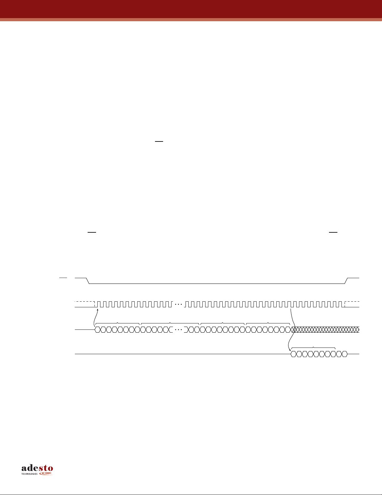
8.2 Dual-Input Byte/Page Program
The Dual-Input Byte/Page Program command is similar to the standard Byte/Page Program command and can be used
to program anywhere from a single byte of data up to 256 bytes of data into previously erased memory locations. Unlike
the standard Byte/Page Program command, the Dual-Input Byte/Page Program command allows two bits of data to be
clocked into the device on every clock cycle rather than just one.
Before the Dual-Input Byte/Page Program command can be started, the Write Enable command must have been
previously issued to the device (see “Write Enable” on page 24) to set the Write Enable Latch (WEL) bit of the Status
Register to a Logical 1 state. To perform a Dual-Input Byte/Page Program command, an opcode of A2h must be clocked
into the device followed by the three address bytes denoting the first byte location of the memory array to begin
programming at. After the address bytes have been clocked in, data can then be clocked into the device two bits at a time
on both the I/O
The data is always input with the MSB of a byte first, and the MSB is always input on the I/O
cycle, bit 7 of the first data byte would be input on the I/O
pin. During the next clock cycle, bits 5 and 4 of the first data byte would be input on the I/O
The sequence would continue with each byte of data being input after every four clock cycles. Like the standard
Byte/Page Program command, all data clocked into the device is stored in an internal buffer.
If the starting memory address denoted by A23-A0 does not fall on an even 256-byte page boundary (A7-A0 are not
all 0), then special circumstances regarding which memory locations to be programmed will apply. In this situation, any
data that is sent to the device that goes beyond the end of the page will wrap around back to the beginning of the same
page.
Example: If the starting address denoted by A23-A0 is 0000FEh and three bytes of data are sent to the device, then
and I/O0 pins.
1
the first two bytes of data will be programmed at addresses 0000FEh and 0000FFh while the last byte of
data will be programmed at address 000000h. The remaining bytes in the page (addresses 000001h
through 0000FDh) will not be programmed and will remain in the erased state (FFh). In addition, if more
than 256 bytes of data are sent to the device, then only the last 256 bytes sent will be latched into the
internal buffer.
pin. During the first clock
1
pin while bit 6 of the same data byte would be input on the I/O0
1
and I/O0 pins respectively.
1
When the
CS pin is deasserted, the device will take the data stored in the internal buffer and program it into the
appropriate memory array locations based on the starting address specified by A23-A0 and the number of data bytes
sent to the device. If less than 256 bytes of data were sent to the device, then the remaining bytes within the page will not
be programmed and will remain in the erased state (FFh). The programming of the data bytes is internally self-timed and
should take place in a time of t
The three address bytes and at least one complete byte of data must be clocked into the device before the
deasserted and the
CS pin must be deasserted on even byte boundaries (multiples of eight bits); otherwise, the device
or tBP if only programming a single byte.
PP
CS pin is
will abort the operation and no data will be programmed into the memory array. In addition, if the address specified by
A23-A0 points to a memory location within a sector that is in the protected state (see “Protect Sector” on page 26) or
locked down (see “Sector Lockdown” on page 32), then the Byte/Page Program command will not be executed and the
device will return to the idle state once the
CS pin has been deasserted. The WEL bit in the Status Register will be reset
back to the Logical 0 state if the program cycle aborts due to an incomplete address being sent, an incomplete byte of
data being sent, the
CS pin being deasserted on non-byte boundaries or because the memory location to be
programmed is protected or locked down.
While the device is programming, the Status Register can be read and will indicate that the device is busy. For faster
throughput, it is recommended that the Status Register be polled rather than waiting the t
or tPP time to determine if the
BP
data bytes have finished programming. At some point before the program cycle completes, the WEL bit in the Status
Register will be reset back to the Logical 0 state.
The device also incorporates an intelligent programming algorithm that can detect when a byte location fails to program
properly. If a programming error arises, it will be indicated by the EPE bit in the Status Register.
AT25DQ321 [DATASHEET]
8718D–DFLASH–12/2012
15
Page 16
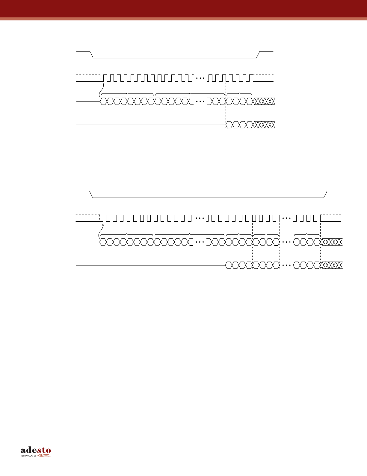
Figure 8-3. Dual-Input Byte Program
CS
2310
SCK
Opcode
SI (I/O0)
SO (I/O1)
10100010
MSB MSB
High-impedance
Figure 8-4. Dual-Input Page Program
CS
2310
SCK
Opcode
SI (I/O0)
10100010
MSB MSB
675410119812 33353431 3229 30
Address Bits A23-A0
AAAA AAAAA
675410119812 3937 3833 36353431 3229 30
Address Bits A23-A0
AAAA AAAAA
Input
Data Byte
D
D
6
4
D
D
7
5
MSB
Input
Data Byte 1
D
D
6
4
D
D
2
0
D
D
3
1
Input
Data Byte 2
D
D
D
D
D
2
0
6
D
4
2
0
Input
Data Byte n
D
D
6
4
D
D
2
0
SO (I/O1)
High-impedance
D
D
D
D
7
5
MSB MSB
D
3
1
D
D
7
D
5
3
1
D
MSB
D
D
7
D
5
3
1
AT25DQ321 [DATASHEET]
8718D–DFLASH–12/2012
16
Page 17

8.3 Quad-Input Byte/Page Program
The Quad-Input Byte/Page Program command is similar to the Dual-Input Byte/Page Program command and can be
used to program anywhere from a single byte of data up to 256 bytes of data into previously erased memory locations.
Unlike the Dual-Input Byte/Page Program command, the Quad-Input Byte/Page Program command allows four bits of
data to be clocked into the device on every clock cycle rather than two.
Before the Quad-Input Byte/Page Program command can be started, the Write Enable command must have been
previously issued to the device (See “Write Enable” on page 24) to set the Write Enable Latch (WEL) bit of the Status
Register to a Logical 1 state. To perform a Quad-Input Byte/Page Program command, an opcode of 32h must be
clocked into the device followed by the three address bytes denoting the first byte location of the memory array to begin
programming at. After the address bytes have been clocked in, data can then be clocked into the device four bits at a
time on the I/O
The data is always input with the MSB of a byte first, and the MSB is always input on the I/O
cycle, bit 7 of the first data byte would be input on the I/O
on the I/O
2
input on the I/O
after every two clock cycles. Like the standard Byte/Page Program and Dual-Input Byte/Page Program commands, all
data clocked into the device is stored in an internal buffer.
If the starting memory address denoted by A23-A0 does not fall on a 256-byte page boundary (A7-A0 are not all 0), then
special circumstances regarding which memory locations to be programmed will apply. In this situation, any data that is
sent to the device that goes beyond the end of the page will wrap around back to the beginning of the same page.
Example: If the starting address denoted by A23-A0 is 0000FEh and three bytes of data are sent to the device, then
pins.
3-0
, I/O1, and I/O0 pins, respectively. During the next clock cycle, bits 3, 2, 1, and 0 of the first data byte would be
, I/O2, I/O1, and I/O0 pins, respectively. The sequence would continue with each byte of data being input
3
the first two bytes of data will be programmed at addresses 0000FEh and 0000FFh while the last byte of
data will be programmed at address 000000h. The remaining bytes in the page (addresses 000001h
through 0000FDh) will not be programmed and will remain in the erased state (FFh). In addition, if more
than 256 bytes of data are sent to the device, then only the last 256 bytes sent will be latched into the
internal buffer.
pin. During the first clock
3
pin while bits 6, 5, and 4 of the same data byte would be input
3
When the
CS pin is deasserted, the device will take the data stored in the internal buffer and program it into the
appropriate memory array locations based on the starting address specified by A23-A0 and the number of data bytes
sent to the device. If less than 256 bytes of data were sent to the device, then the remaining bytes within the page will
not be programmed and will remain in the erased state (FFh). The programming of the data bytes is internally self-timed
and should take place in a time of t
The three address bytes and at least one complete byte of data must be clocked into the device before the
deasserted and the
CS pin must be deasserted on byte boundaries (multiples of eight bits); otherwise, the device will
or tBP if only programming a single byte.
PP
CS pin is
abort the operation and no data will be programmed into the memory array. In addition, if the address specified by
A23-A0 points to a memory location within a sector that is in the protected state (See “Protect Sector” on page 26) or
locked down (See “Sector Lockdown” on page 32), then the Quad-Input Byte/Page Program command will not be
executed and the device will return to the idle state once the
CS pin has been deasserted. The WEL bit in the Status
Register will be reset back to the Logical 0 state if the program cycle aborts due to an incomplete address being sent, an
incomplete byte of data being sent, the
CS pin being deasserted on non-byte boundaries or because the memory
location to be programmed is protected or locked down.
While the device is programming, the Status Register can be read and will indicate that the device is busy. For faster
throughput, it is recommended that the Status Register be polled rather than waiting the t
or tPP time to determine if the
BP
data bytes have finished programming. At some point before the program cycle completes, the WEL bit in the Status
Register will be reset back to the Logical 0 state.
The device also incorporates an intelligent programming algorithm that can detect when a byte location fails to program
properly. If a programming error arises, it will be indicated by the EPE bit in the Status Register.
AT25DQ321 [DATASHEET]
8718D–DFLASH–12/2012
17
Page 18
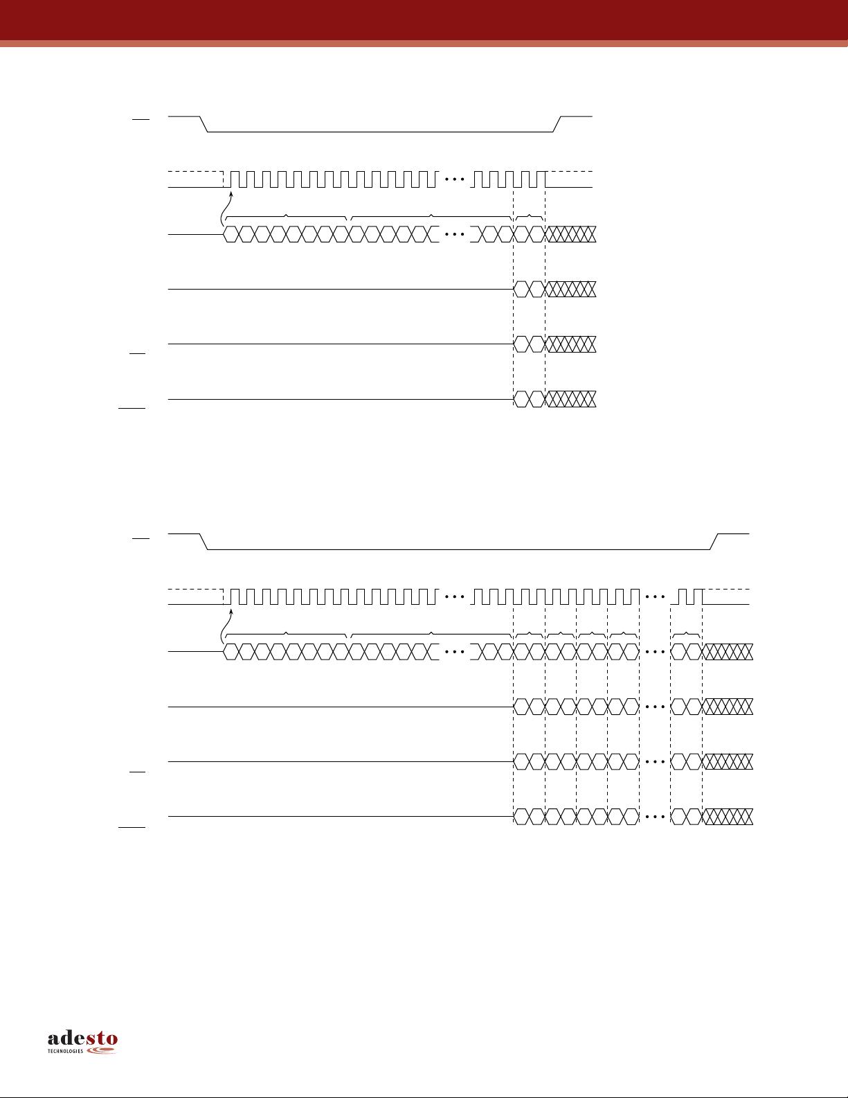
Figure 8-5. Quad-Input Byte Program
CS
2310
SCK
Opcode
I/O
I/O
0
(SI)
1
00110010
MSB MSB
High-impedance
(SO)
I/O
2
High-impedance
(WP)
I/O
3
High-impedance
(HOLD)
Figure 8-6. Quad-Input Page Program
CS
675410119812 3331 3229 30
Address Bits A23-A0
AAAA AAAAA
D
D
D6D
D7D
MSB
Byte
4
5
IN
D
0
D
1
2
3
SCK
I/O
(SI)
I/O
(SO)
I/O
(WP)
I/O
(HOLD)
2310
Opcode
0
1
00110010
MSB MSB
High-impedance
High-impedance
2
High-impedance
3
675410119812 3937 3833 36353431 3229 30
Address Bits A23-A0
AAAA AAAAA
Byte 1INByte 2INByte 3INByte 4
D
D
D
D
D
D
4
0
D
D
D
1
5
D6D
D6D
2
D7D
D7D
3
MSB MSB MSBMSB
4
0
D
5
1
2
3
4
D
5
D6D
D7D
D
0
D
D
1
D6D
2
D7D
3
IN
D
4
0
D
5
1
2
3
Byte n
D
D
D6D
D7D
MSB
IN
D
4
0
D
5
1
2
3
AT25DQ321 [DATASHEET]
8718D–DFLASH–12/2012
18
Page 19
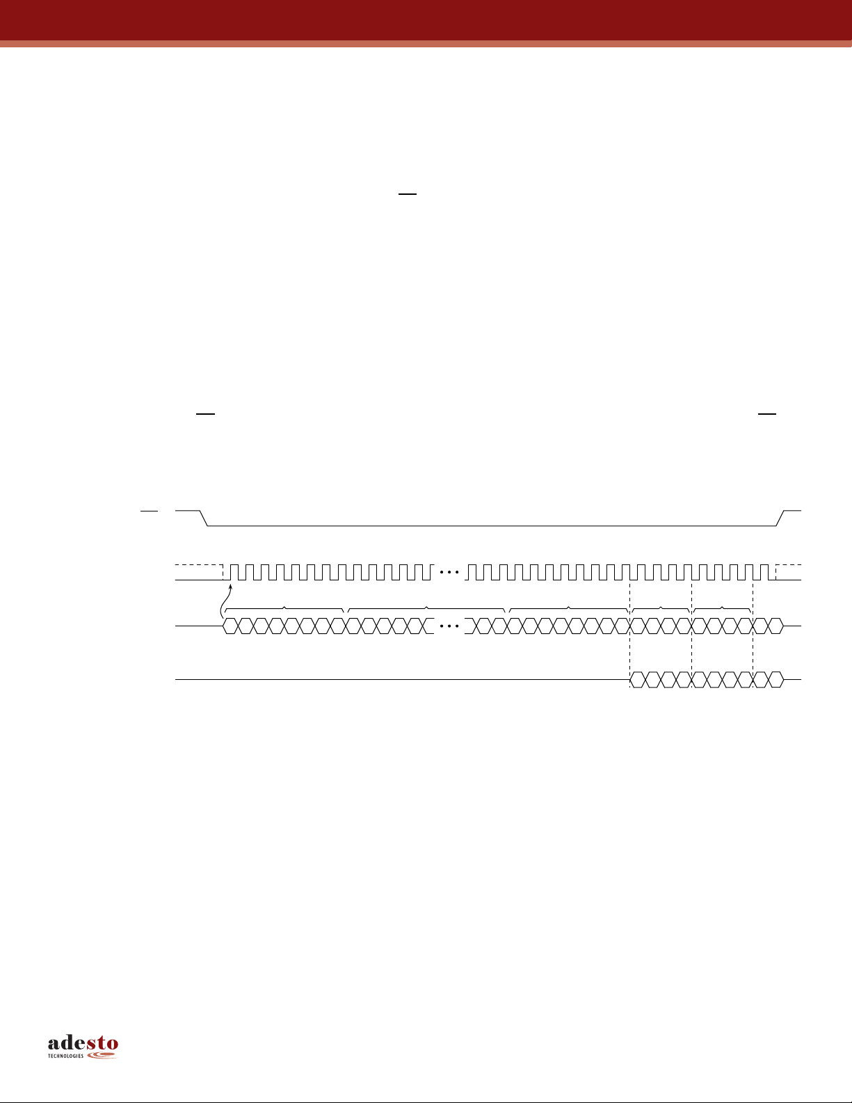
8.4 Block Erase
A block of 4, 32, or 64 KB can be erased (all bits set to the Logical 1 state) in a single operation by using one of three
different opcodes for the Block Erase command. An opcode of 20h is used for a 4KB erase, an opcode of 52h is used for
a 32KB erase and an opcode of D8h is used for a 64KB erase. Before a Block Erase command can be started, the Write
Enable command must have been previously issued to the device to set the WEL bit of the Status Register to a Logical 1
state.
To perform a Block Erase, the CS pin must first be asserted and the appropriate opcode (20h, 52h, or D8h) must be
clocked into the device. After the opcode has been clocked in, the three address bytes specifying an address within the
4KB, 32KB, or 64KB block to be erased must be clocked in. Any additional data clocked into the device will be ignored.
When the
self-timed and should take place in a time of t
Since the Block Erase command erases a region of bytes, the lower order address bits do not need to be decoded by the
device. Therefore, for a 4KB erase, address bits A11-A0 will be ignored by the device and their values can be either a
Logical 1 or 0. For a 32KB erase, address bits A14-A0 will be ignored and for a 64KB erase, address bits A15-A0 will be
ignored by the device. Despite the lower order address bits not being decoded by the device, the complete three address
bytes must still be clocked into the device before the CS pin is deasserted and the CS pin must be deasserted on a byte
boundary (multiples of eight bits); otherwise, the device will abort the operation and no erase operation will be performed.
If the address specified by A23-A0 points to a memory location within a sector that is in the protected or locked down
state, then the Block Erase command will not be executed and the device will return to the idle state once the
been deasserted.
The WEL bit in the Status Register will be reset back to the Logical 0 state if the erase cycle aborts due to an incomplete
address being sent, the
region to be erased is protected or locked down.
While the device is executing a successful erase cycle, the Status Register can be read and will indicate that the device
is busy. For faster throughput, it is recommended that the Status Register be polled rather than waiting the t
determine if the device has finished erasing. At some point before the erase cycle completes, the WEL bit in the Status
Register will be reset back to the Logical 0 state.
The device also incorporates an intelligent erase algorithm that can detect when a byte location fails to erase properly. If
an erase error occurs, it will be indicated by the EPE bit in the Status Register.
CS pin is deasserted, the device will erase the appropriate block. The erasing of the block is internally
.
BLKE
CS pin has
CS pin being deasserted on non-byte boundaries or because a memory location within the
time to
BLKE
Figure 8-7. Block Erase
CS
SCK
SI
SO
CCCCCCCC
MSB MSB
High-impedance
2310
Opcode
675410119812 3129 3027 2826
Address Bits A23-A0
AAAA AAAAA A A A
AT25DQ321 [DATASHEET]
8718D–DFLASH–12/2012
19
Page 20
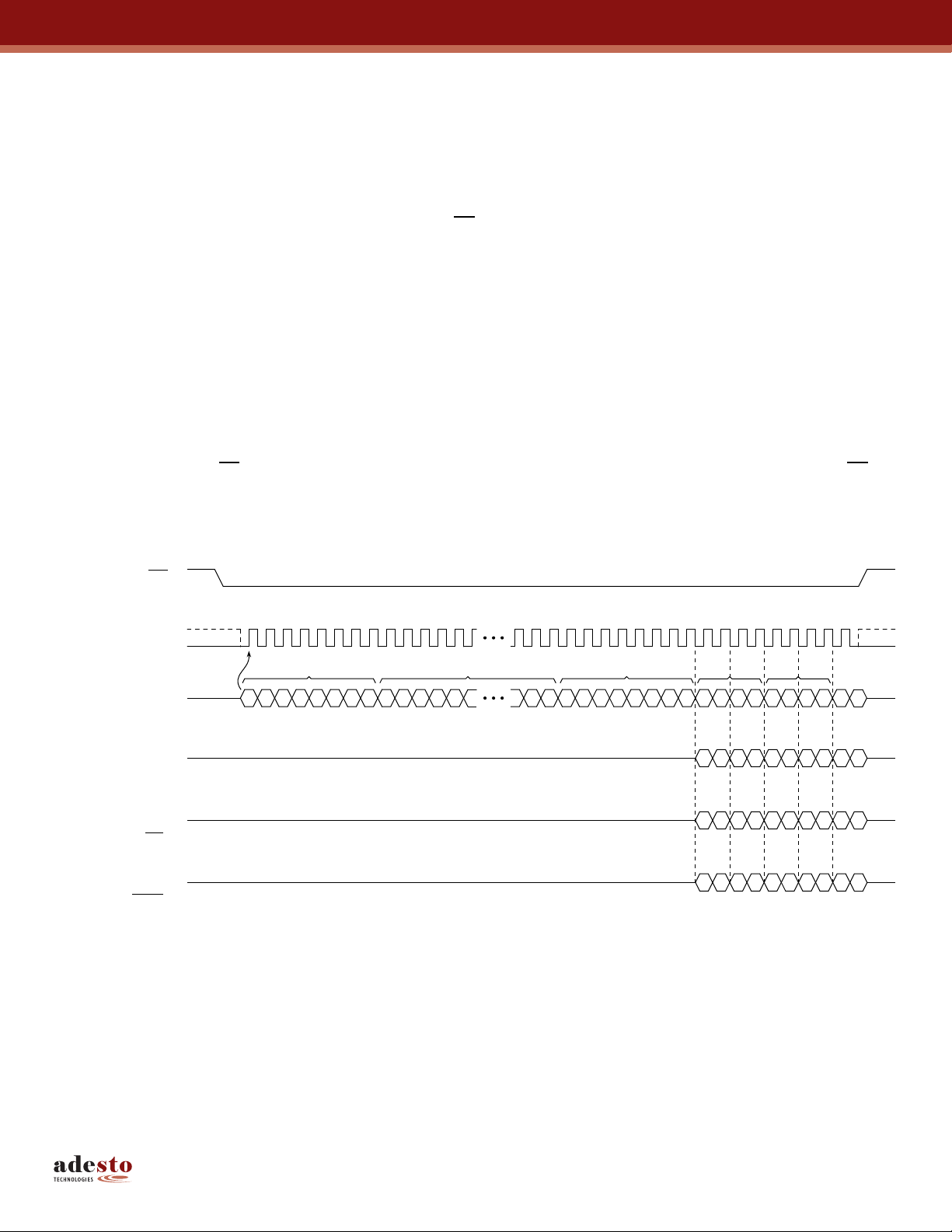
8.5 Chip Erase
The entire memory array can be erased in a single operation by using the Chip Erase command. Before a Chip Erase
command can be started, the Write Enable command must have been previously issued to the device to set the WEL bit
of the Status Register to a Logical 1 state.
Two opcodes, 60h and C7h, can be used for the Chip Erase command. There is no difference in device functionality
when utilizing the two opcodes, so they can be used interchangeably. To perform a Chip Erase, one of the two opcodes
(60h or C7h) must be clocked into the device. Since the entire memory array is to be erased, no address bytes need to
be clocked into the device and any data clocked in after the opcode will be ignored. When the
device will erase the entire memory array. The erasing of the device is internally self-timed and should take place in a
time of t
The complete opcode must be clocked into the device before the
deasserted on a byte boundary (multiples of eight bits); otherwise, no erase will be performed. In addition, if any sector of
the memory array is in the protected or locked down state, then the Chip Erase command will not be executed and the
device will return to the idle state once the
back to the Logical 0 state if the
down state.
While the device is executing a successful erase cycle, the Status Register can be read and will indicate that the device
is busy. For faster throughput, it is recommended that the Status Register be polled rather than waiting the t
determine if the device has finished erasing. At some point before the erase cycle completes, the WEL bit in the Status
Register will be reset back to the Logical 0 state.
The device also incorporates an intelligent erase algorithm that can detect when a byte location fails to erase properly. If
an erase error occurs, it will be indicated by the EPE bit in the Status Register.
CHPE
.
CS pin is deasserted, the
CS pin is deasserted and the CS pin must be
CS pin has been deasserted. The WEL bit in the Status Register will be reset
CS pin is deasserted on non-byte boundaries or if a sector is in the protected or locked
time to
CHPE
Figure 8-8. Chip Erase
CS
SCK
SI
SO
CCCCCCCC
MSB
High-impedance
2310
Opcode
6754
AT25DQ321 [DATASHEET]
8718D–DFLASH–12/2012
20
Page 21

8.6 Program/Erase Suspend
In some code plus data storage applications, it is often necessary to process certain high-level system interrupts that
require relatively immediate reading of code or data from the Flash memory. In such an instance, it may not be possible
for the system to wait the microseconds or milliseconds required for the Flash memory to complete a program or erase
cycle. The Program/Erase Suspend command allows a program or erase operation in progress to a particular 64KB
sector of the Flash memory array to be suspended so that other device operations can be performed.
Example: By suspending an erase operation to a particular sector, the system can perform functions such as a
program or read operation within another 64KB sector in the device. Other device operations, such as a
Read Status Register, can also be performed while a program or erase operation is suspended. Table 8-1
outlines the operations that are allowed and not allowed during a program or erase suspend.
Since the need to suspend a program or erase operation is immediate, the Write Enable command does not need to be
issued prior to the Program/Erase Suspend command being issued. Therefore, the Program/Erase Suspend command
operates independently of the state of the WEL bit in the Status Register.
To perform a Program/Erase Suspend, the
device. No address bytes need to be clocked into the device and any data clocked in after the opcode will be ignored.
When the
t
SUSP
Logical 1 state to indicate that the program or erase operation has been suspended. In addition, the RDY/BSY bit in the
Status Register will indicate that the device is ready for another operation. The complete opcode must be clocked into
the device before the
bits); otherwise, no suspend operation will be performed.
If the Program/Erase Suspend command is issued while the device is not busy performing a program or erase operation,
(CRDY/BSY is in the Logic 1 state), then the device is simply ignore the Program/Erase Suspend command and the PS
and ES bits in the status Register will indicate that the device is not in a suspend state, (PS and ES will be a Logic 0).
Read operations are not allowed to a 64KB sector that has had its program or erase operation suspended. If a read is
attempted to a suspended sector, then the device will output undefined data. Therefore, when performing a Read Array
operation to an unsuspended sector and the device’s internal address counter increments and crosses the sector
boundary to a suspended sector, the device will then start outputting undefined data continuously until the address
counter increments and crosses a sector boundary to an unsuspended sector.
A program operation is not allowed to a sector that has been erase suspended. If a program operation is attempted to an
erase suspended sector, then the program operation will abort and the WEL bit in the Status Register will be reset back
to the Logical 0 state. Likewise, an erase operation is not allowed to a sector that has been program suspended. If
attempted, the erase operation will abort and the WEL bit in the Status Register will be reset to a Logical 0 state.
During an Erase Suspend, a program operation to a different 64KB sector can be started and subsequently suspended.
This results in a simultaneous Erase Suspend/Program Suspend condition and will be indicated by the states of both the
ES and PS bits in the Status Register being set to the Logical 1 state.
If a Reset operation (see “Reset” on page 48) is performed while a sector is erase suspended, the suspend operation will
abort and the contents of the block in the suspended sector will be left in an undefined state. However, if a Reset is
performed while a sector is program suspended, the suspend operation will abort but only the contents of the page that
was being programmed and subsequently suspended will be undefined. The remaining pages in the 64KB sector will
retain their previous contents.
If an attempt is made to perform an operation that is not allowed during a program or erase suspend, such as a Protect
Sector operation, then the device will simply ignore the opcode and no operation will be performed. The state of the WEL
bit in the Status Register, as well as the SPRL (Sector Protection Registers Locked) and SLE (Sector Lockdown
Enabled) bits, will not be affected.
CS pin is deasserted, the program or erase operation currently in progress will be suspended within a time of
. The Program Suspend (PS) bit or the Erase Suspend (ES) bit in the Status Register will then be set to the
CS pin is deasserted and the CS pin must be deasserted on non-byte boundary (multiples of eight
CS pin must first be asserted and the opcode of B0h must be clocked into the
AT25DQ321 [DATASHEET]
8718D–DFLASH–12/2012
21
Page 22
Table 8-1. Operations Allowed and Not Allowed During a Program or Erase Suspend
Command
Operation During
Program Suspend
Operation During
Erase Suspend
Read Commands
Read Array (All Opcodes) Allowed Allowed
Program and Erase Commands
Block Erase Not Allowed Not Allowed
Chip Erase Not Allowed Not Allowed
Byte/Page Program (All Opcodes) Not Allowed Allowed
Program/Erase Suspend Not Allowed Allowed
Program/Erase Resume Allowed Allowed
Protection Commands
Write Enable Not Allowed Allowed
Write Disable Not Allowed Allowed
Protect Sector Not Allowed Not Allowed
Unprotect Sector Not Allowed Not Allowed
Global Protect/Unprotect Not Allowed Not Allowed
Read Sector Protection Registers Allowed Allowed
Security Commands
Sector Lockdown Not Allowed Not Allowed
Freeze Sector Lockdown State Not Allowed Not Allowed
Read Sector Lockdown Registers Allowed Allowed
Program OTP Security Register Not Allowed Not Allowed
Read OTP Security Register Allowed Allowed
Status and Configuration Register Commands
Read Status Register Allowed Allowed
Write Status Register (All Opcodes) Not Allowed Not Allowed
Read Configuration Register Allowed Allowed
Write Configuration Register Not Allowed Not Allowed
Miscellaneous Commands
Reset Allowed Allowed
Read Manufacturer and Device ID Allowed Allowed
Deep Power-Down Not Allowed Not Allowed
Resume from Deep Power-Down Not Allowed Not Allowed
Figure 8-9. Program/Erase Suspend
CS
2310
SCK
Opcode
SI
SO
10110000
MSB
High-impedance
6754
AT25DQ321 [DATASHEET]
8718D–DFLASH–12/2012
22
Page 23
8.7 Program/Erase Resume
The Program/Erase Resume command allows a suspended program or erase operation to be resumed and continue
programming a Flash page or erasing a Flash memory block where it left off. As with the Program/Erase Suspend
command, the Write Enable command does not need to be issued prior to the Program/Erase Resume command being
issued. Therefore, the Program/Erase Resume command operates independently of the state of the WEL bit in the
Status Register.
To perform a Program/Erase Resume, the CS pin must first be asserted and the opcode of D0h must be clocked into the
device. No address bytes need to be clocked into the device and any data clocked in after the opcode will be ignored.
When the
t
RES
program or erase operation is no longer suspended. In addition, the RDY/BSY bit in the Status Register will indicate that
the device is busy performing a program or erase operation. The complete opcode must be clocked into the device
before the
otherwise, no resume operation will be performed.
During a simultaneous Erase Suspend/Program Suspend condition, issuing the Program/Erase Resume command will
result in the program operation resuming first. After the program operation has been completed, the Program/Erase
Resume command must be issued again in order for the erase operation to be resumed.
While the device is busy resuming a program or erase operation, any attempts at issuing the Program/Erase Suspend
command will be ignored. Therefore, if a resumed program or erase operation needs to be subsequently suspended
again, the system must either wait the entire t
check the status of the RDY/BSY bit or the appropriate PS or ES bit in the Status Register to determine if the previously
suspended program or erase operation has resumed.
CS pin is deasserted, the program or erase operation currently suspended will be resumed within a time of
. The PS bit or the ES bit in the Status Register will then be reset back to the Logical 0 state to indicate that the
CS pin is deasserted and the CS pin must be deasserted on a byte boundary (multiples of eight bits);
time before issuing the Program/Erase Suspend command, or it must
RES
Figure 8-10. Program/Erase Resume
CS
2310
SCK
Opcode
SI
SO
11010000
MSB
High-impedance
6754
AT25DQ321 [DATASHEET]
8718D–DFLASH–12/2012
23
Page 24
9. Protection Commands and Features
9.1 Write Enable
The Write Enable command is used to set the Write Enable Latch (WEL) bit in the Status Register to a Logical 1 state.
The WEL bit must be set before a Byte/Page Program, Erase, Protect Sector, Unprotect Sector, Sector Lockdown,
Freeze Sector Lockdown State, Program OTP Security Register, Write Status Register, or Write Configuration Register
command can be executed. This makes the issuance of these commands a two step process, thereby reducing the
chances of a command being accidentally or erroneously executed. If the WEL bit in the Status Register is not set prior to
the issuance of one of these commands, then the command will not be executed.
To issue the Write Enable command, the
device. No address bytes need to be clocked into the device and any data clocked in after the opcode will be ignored.
When the
CS pin is deasserted, the WEL bit in the Status Register will be set to a Logical 1. The complete opcode must
be clocked into the device before the
(multiples of eight bits); otherwise, the device will abort the operation and the state of the WEL bit will not change.
Figure 9-1. Write Enable
CS
CS pin must first be asserted and the opcode of 06h must be clocked into the
CS pin is deasserted and the CS pin must be deasserted on an even byte boundary
SCK
SI
SO
2310
Opcode
00000110
MSB
High-impedance
6754
AT25DQ321 [DATASHEET]
8718D–DFLASH–12/2012
24
Page 25
9.2 Write Disable
The Write Disable command is used to reset the Write Enable Latch (WEL) bit in the Status Register to the Logical 0
state. With the WEL bit reset, all Byte/Page Program, Erase, Protect Sector, Unprotect Sector, Sector Lockdown, Freeze
Sector Lockdown State, Program OTP Security Register, Write Status Register, and Write Configuration Register
commands will not be executed. Other conditions can also cause the WEL bit to be reset; for more details, refer to the
WEL bit section of the Status Register description.
To issue the Write Disable command, the CS pin must first be asserted and the opcode of 04h must be clocked into the
device. No address bytes need to be clocked into the device and any data clocked in after the opcode will be ignored.
When the
must be clocked into the device before the
(multiples of eight bits); otherwise, the device will abort the operation and the state of the WEL bit will not change.
Figure 9-2. Write Disable
CS pin is deasserted, the WEL bit in the Status Register will be reset to a Logical 0. The complete opcode
CS
CS pin is deasserted and the CS pin must be deasserted on a byte boundary
SCK
SI
SO
2310
Opcode
00000100
MSB
High-impedance
6754
AT25DQ321 [DATASHEET]
8718D–DFLASH–12/2012
25
Page 26

9.3 Protect Sector
Every physical 64KB sector of the device has a corresponding single-bit Sector Protection Register that is used to control
the software protection of a sector. Upon device power-up, each Sector Protection Register will default to the Logical 1
state indicating that all sectors are protected and cannot be programmed or erased.
Issuing the Protect Sector command to a particular sector address will set the corresponding Sector Protection Register
to the Logical 1 state. The following table outlines the two states of the Sector Protection Registers.
Table 9-1. Sector Protection Register Values
Value Sector Protection Status
0 Sector is unprotected and can be programmed and erased.
1 Sector is protected and cannot be programmed or erased. This is the default state.
Before the Protect Sector command can be issued, the Write Enable command must have been previously issued to set
the WEL bit in the Status Register to a Logical 1. To issue the Protect Sector command, the
and the opcode of 36h must be clocked into the device followed by three address bytes designating any address within
the sector to be protected. Any additional data clocked into the device will be ignored. When the
the Sector Protection Register corresponding to the physical sector addressed by A23-A0 will be set to the Logical 1
state and the sector itself will then be protected from program and erase operations. In addition, the WEL bit in the Status
Register will be reset back to the Logical 0 state.
The complete three address bytes must be clocked into the device before the
be deasserted on an even byte boundary (multiples of eight bits); otherwise, the device will abort the operation. When the
device aborts the Protect Sector operation, the state of the Sector Protection Register will be unchanged and the WEL bit
in the Status Register will be reset to a Logical 0.
As a safeguard against accidental or erroneous protecting or unprotecting of sectors, the Sector Protection Registers can
themselves be locked from updates by using the SPRL (Sector Protection Registers Locked) bit of the Status Register
See Status RegisterSee “Status Register Commands” on page 39 description for more details). If the Sector Protection
(
Registers are locked, then any attempts to issue the Protect Sector command will be ignored and the device will reset the
WEL bit in the Status Register back to a Logical 0 and return to the idle state once the
CS pin must first be asserted
CS pin is deasserted,
CS pin is deasserted and the CS pin must
CS pin has been deasserted.
Figure 9-3. Protect Sector
CS
SCK
SI
SO
00110
06% 06%
High-impedance
2310
Opcode
675410119812 3129 3027 2826
Address Bits A23-A0
AAAA AAAAA A A A
101
AT25DQ321 [DATASHEET]
8718D–DFLASH–12/2012
26
Page 27

9.4 Unprotect Sector
Issuing the Unprotect Sector command to a particular sector address will reset the corresponding Sector Protection
Register to the Logical 0 state (see Table 9-1 for Sector Protection Register values). Every physical sector of the device
has a corresponding single-bit Sector Protection Register that is used to control the software protection of a sector.
Before the Unprotect Sector command can be issued, the Write Enable command must have been previously issued to
set the WEL bit in the Status Register to a Logical 1. To issue the Unprotect Sector command, the
asserted and the opcode of 39h must be clocked into the device. After the opcode has been clocked in, the three address
bytes designating any address within the sector to be unprotected must be clocked in. Any additional data clocked into
the device after the address bytes will be ignored. When the
corresponding to the sector addressed by A23-A0 will be reset to the Logical 0 state and the sector itself will be
unprotected. In addition, the WEL bit in the Status Register will be reset back to the Logical 0 state.
The complete three address bytes must be clocked into the device before the
be deasserted on a byte boundary (multiples of eight bits); otherwise, the device will abort the operation, the state of the
Sector Protection Register will be unchanged and the WEL bit in the Status Register will be reset to a Logical 0.
As a safeguard against accidental or erroneous locking or unlocking of sectors, the Sector Protection Registers can
themselves be locked from updates by using the SPRL (Sector Protection Registers Locked) bit of the Status Register
(please refer to the Status Register description for more details). If the Sector Protection Registers are locked, then any
attempts to issue the Unprotect Sector command will be ignored and the device will reset the WEL bit in the Status
Register back to a Logical 0 and return to the idle state once the
Figure 9-4. Unprotect Sector
CS pin must first be
CS pin is deasserted, the Sector Protection Register
CS pin is deasserted and the CS pin must
CS pin has been deasserted.
CS
SCK
SI
SO
2310
Opcode
00111
06% 06%
High-impedance
675410119812 3129 3027 2826
010
Address Bits A23-A0
AAAA AAAAA A A A
AT25DQ321 [DATASHEET]
8718D–DFLASH–12/2012
27
Page 28

9.5 Global Protect/Unprotect
The Global Protect and Global Unprotect features can work in conjunction with the Protect Sector and Unprotect Sector
functions.
Example: A system can globally protect the entire memory array and then use the Unprotect Sector command to
individually unprotect certain sectors and individually reprotect them later by using the Protect Sector
command. Likewise, a system can globally unprotect the entire memory array and then individually protect
certain sectors as needed.
Performing a Global Protect or Global Unprotect is accomplished by writing a certain combination of data to the Status
Register using the Write Status Register Byte 1 command (see “Write Status Register Byte 1” on page 43 for command
execution details). The Write Status Register command is also used to modify the SPRL (Sector Protection Registers
Locked) bit to control hardware and software locking.
To perform a Global Protect, the appropriate
Logical 1 to bits 5, 4, 3, and 2 of the first byte of the Status Register. Conversely, to perform a Global Unprotect, the same
WP and SPRL conditions must be met but the system must write a Logical 0 to bits 5, 4, 3, and 2 of the first byte of the
Status Register. Table 9-2 details the conditions necessary for a Global Protect or Global Unprotect to be performed.
Sectors that have been erase or program suspended must remain in the unprotected state. If a Global Protect operation
is attempted while a sector is erase or program suspended, the protection operation will abort, the protection states of all
sectors in the Flash memory array will not change and WEL bit in the Status Register will be reset back to a Logical 0.
Essentially, if the SPRL bit of the Status Register is in the Logical 0 state (Sector Protection Registers are not locked),
then writing a 00h to the first byte of the Status Register will perform a Global Unprotect without changing the state of the
SPRL bit. Similarly, writing a 7Fh to the first byte of the Status Register will perform a Global Protect and keep the SPRL
bit in the Logical 0 state. The SPRL bit can, of course, be changed to a Logical 1 by writing an FFh if software-locking or
hardware-locking is desired along with the Global Protect.
If the desire is to only change the SPRL bit without performing a Global Protect or Global Unprotect, then the system can
simply write a 0Fh to the first byte of the Status Register to change the SPRL bit from a Logical 1 to a Logical 0 provided
the
WP pin is deasserted. Likewise, the system can write an F0h to change the SPRL bit from a Logical 0 to a Logical 1
without affecting the current sector protection status (no changes will be made to the Sector Protection Registers).
When writing to the first byte of the Status Register, bits 5, 4, 3, and 2 will not actually be modified but will be decoded by
the device for the purposes of the Global Protect and Global Unprotect functions. Only bit 7, the SPRL bit, will actually be
modified. Therefore, when reading the first byte of the Status Register, bits 5, 4, 3, and 2 will not reflect the values written
to them but will instead indicate the status of the WP pin and the sector protection status. Please refer to “Read Status
Register” on page 39 and Table 11-1 on page 39 for details on the Status Register format and what values can be read
for bits 5, 4, 3, and 2.
WP pin and SPRL conditions must be met and the system must write a
AT25DQ321 [DATASHEET]
8718D–DFLASH–12/2012
28
Page 29

Table 9-2. Valid SPRL and Global Protect/Unprotect Conditions
New Write Status
Register Byte 1
Data
Bit
7 6 5 4 3 2 1 0
Protection Operation
WP
State
Current
SPRL
Value
New
SPRL
Value
0 x 0 0 0 0 x x
0 x 0 0 0 1 x x
0 x 1 1 1 0 x x
0 x 1 1 1 1 x x
0 0
1 x 0 0 0 0 x x
1 x 0 0 0 1 x x
1 x 1 1 1 0 x x
1 x 1 1 1 1 x x
0 1 x x x x x x x x
0 x 0 0 0 0 x x
0 x 0 0 0 1 x x
0 x 1 1 1 0 x x
0 x 1 1 1 1 x x
1 0
1 x 0 0 0 0 x x
1 x 0 0 0 1 x x
1 x 1 1 1 0 x x
1 x 1 1 1 1 x x
Global Unprotect – all Sector Protection Registers reset to 0
No change to current protection
No change to current protection
No change to current protection
Global Protect – all Sector Protection Registers set to 1
Global Unprotect – all Sector Protection Registers reset to 0
No change to current protection
No change to current protection
No change to current protection
Global Protect – all Sector Protection Registers set to 1
No change to the current protection level. All sectors currently protected will remain protected
and all sectors currently unprotected will remain unprotected.
The Sector Protection Registers are hard-locked and cannot be changed when the WP pin is
LOW and the current state of SPRL is 1. Therefore, a Global Protect/Unprotect will not occur.
In addition, the SPRL bit cannot be changed (the WP pin must be HIGH in order to change
SPRL back to a 0).
Global Unprotect – all Sector Protection Registers reset to 0
No change to current protection
No change to current protection
No change to current protection
Global Protect – all Sector Protection Registers set to 1
Global Unprotect – all Sector Protection Registers reset to 0
No change to current protection
No change to current protection
No change to current protection
Global Protect – all Sector Protection Registers set to 1
0
0
0
0
0
1
1
1
1
1
0
0
0
0
0
1
1
1
1
1
1 1
0 x 0 0 0 0 x x
0 x 0 0 0 1 x x
0 x 1 1 1 0 x x
0 x 1 1 1 1 x x
1 x 0 0 0 0 x x
1 x 0 0 0 1 x x
1 x 1 1 1 0 x x
1 x 1 1 1 1 x x
No change to the current protection level. All sectors currently protected will remain
protected and all sectors currently unprotected will remain unprotected.
The Sector Protection Registers are soft-locked and cannot be changed when the
current state of SPRL is 1. Therefore, a Global Protect/Unprotect will not occur.
However, the SPRL bit can be changed back to a 0 from a 1 since the WP pin is
HIGH. To perform a Global Protect/Unprotect, the Write Status Register command
must be issued again after the SPRL bit has been changed from a 1 to a 0.
AT25DQ321 [DATASHEET]
8718D–DFLASH–12/2012
0
0
0
0
0
1
1
1
1
1
29
Page 30

9.6 Read Sector Protection Registers
The Sector Protection Registers can be read to determine the current software protection status of each sector. Reading
the Sector Protection Registers, however, will not determine the status of the
To read the Sector Protection Register for a particular sector, the
must be clocked in. Once the opcode has been clocked in, three address bytes designating any address within the sector
must be clocked in. After the last address byte has been clocked in, the device will begin outputting data on the SO pin
during every subsequent clock cycle. The data being output will be a repeating byte of either FFh or 00h to denote the
value of the appropriate Sector Protection Register.
At clock frequencies above f
above f
, at least two bytes of data must be clocked out from the device in order to determine the correct status of the
CLK
appropriate Sector Protection Register.
Table 9-3. Read Sector Protection Register - Output Data
Output Data Sector Protection Register Value
00h Sector Protection Register Value is 0 (Sector is Unprotected).
FFh Sector Protection Register Value is 1 (Sector is Protected).
Deasserting the CS pin will terminate the read operation and put the SO pin into a high-impedance state. The CS pin can
be deasserted at any time and does not require that a full byte of data be read.
In addition to reading the individual Sector Protection Registers, the Software Protection Status (SWP) bits in the Status
Register can be read to determine if all, some or none of the sectors are software protected (See “Read Status Register”
on page 39 for more details).
, the first byte of data output will not be valid. Therefore, if operating at clock frequencies
CLK
WP pin.
CS pin must first be asserted and the opcode of 3Ch
Figure 9-5. Read Sector Protection Register
CS
2310
675410119812 373833 36353431 3229 30 39 40
SCK
Opcode
SI
SO
00111100
MSB MSB
High-impedance
AAAA AAAAA
Address Bits A23-A0
Data Byte
DDDDDDDDDD
MSB MSB
AT25DQ321 [DATASHEET]
8718D–DFLASH–12/2012
30
Page 31

9.7 Protected States and the Write Protect (WP) Pin
The WP pin is not linked to the memory array itself and has no direct effect on the protection status or lockdown status of
the memory array. Instead, the
Status Register, is used to control the hardware locking mechanism of the device. For hardware locking to be active, two
conditions must be met-the
When hardware locking is active, the Sector Protection Registers are locked and the SPRL bit itself is also locked.
Therefore, sectors that are protected will be locked in the protected state and sectors that are unprotected will be locked
in the unprotected state. These states cannot be changed as long as hardware locking is active, so the Protect Sector,
Unprotect Sector, and Write Status Register commands will be ignored. In order to modify the protection status of a
sector, the WP pin must first be deasserted and the SPRL bit in the Status Register must be reset back to the Logical 0
state using the Write Status Register command. When resetting the SPRL bit back to a Logical 0, it is not possible to
perform a Global Protect or Global Unprotect at the same time since the Sector Protection Registers remain soft-locked
until after the Write Status Register command has been executed.
If the
WP pin is permanently connected to GND, then once the SPRL bit is set to a Logical 1, the only way to reset the bit
back to the Logical 0 state is to power-cycle the device. This allows a system to power-up with all sectors software
protected but not hardware locked. Therefore, sectors can be unprotected and protected as needed and then hardware
locked at a later time by simply setting the SPRL bit in the Status Register.
When the
WP pin is deasserted or if the WP pin is permanently connected to VCC, the SPRL bit in the Status Register
can still be set to a Logical 1 to lock the Sector Protection Registers. This provides a software locking ability to prevent
erroneous Protect Sector or Unprotect Sector commands from being processed. When changing the SPRL bit to a
Logical 1 from a Logical 0, it is also possible to perform a Global Protect or Global Unprotect at the same time by writing
the appropriate values into bits 5, 4, 3, and 2 of the first byte of the Status Register.
Tables 9-4 and 9-5 detail the various protection and locking states of the device.
WP pin, in conjunction with the SPRL (Sector Protection Registers Locked) bit in the
WP pin must be asserted and the SPRL bit must be in the Logical 1 state.
Table 9-4. Sector Protection Register States
WP
X
(Don't Care)
Note: 1. “n” represents a sector number.
Table 9-5. Hardware and Software Locking
SPRL Change
WP SPRL Locking
0 0
0 1
1 0
1 1
Hardware
Locked
Software
Locked
Allowed
Can be modified
from 0 to 1
Locked
Can be modified
from 0 to 1
Can be modified
from 1 to 0
Sector Protection Register
(1)
n
0 Unprotected
1 Protected
Sector Protection Registers
Unlocked and modifiable using the Protect and Unprotect Sector
commands. Global Protect and Unprotect can also be performed.
Locked in current state. Protect and Unprotect Sector commands will
be ignored. Global Protect and Unprotect cannot be performed.
Unlocked and modifiable using the Protect and Unprotect Sector
commands. Global Protect and Unprotect can also be performed.
Locked in current state. Protect and Unprotect Sector commands will
be ignored. Global Protect and Unprotect cannot be performed.
Sector
(1)
n
AT25DQ321 [DATASHEET]
8718D–DFLASH–12/2012
31
Page 32

10. Security Commands
10.1 Sector Lockdown
Certain applications require that portions of the Flash memory array be permanently protected against malicious
attempts at altering program code, data modules, security information or encryption/decryption algorithms, keys, and
routines. To address these applications, the device incorporates a sector lockdown mechanism that allows any
combination of individual 64KB sectors to be permanently locked so that they become read-only. Once a sector is locked
down, it can never be erased or programmed again and it can never be unlocked from the locked down state.
Each 64KB physical sector has a corresponding single-bit Sector Lockdown Register that is used to control the lockdown
status of that sector. These registers are nonvolatile and will retain their state even after a device power-cycle or reset
operation. The following table outlines the two states of the Sector Lockdown Registers.
Table 10-1. Sector Lockdown Register Values
Value Sector Lockdown Status
0 Sector is not locked down and can be programmed and erased. This is the default state.
1 Sector is permanently locked down and can never be programmed or erased again.
Issuing the Sector Lockdown command to a particular sector address will set the corresponding Sector Lockdown
Register to the Logical 1 state. Each Sector Lockdown Register can only be set once; therefore, once set to the Logical 1
state, a Sector Lockdown Register cannot be reset back to the Logical 0 state.
Before the Sector Lockdown command can be issued, the Write Enable command must have been previously issued to
set the WEL bit in the Status Register to a Logical 1. In addition, the Sector Lockdown Enabled (SLE) bit in the Status
Register must have also been previously set to the Logical 1 state by using the Write Status Register Byte 2 command
(see “Write Status Register Byte 2” on page 44). To issue the Sector Lockdown command, the
asserted and the opcode of 33h must be clocked into the device followed by three address bytes designating any
address within the 64KB sector to be locked down. After the three address bytes have been clocked in, a confirmation
byte of D0h must also be clocked in immediately following the three address bytes. Any additional data clocked into the
device after the first byte of data will be ignored. When the
corresponding to the sector addressed by A23-A0 will be set to the Logical 1 state and the sector itself will then be
permanently locked down from program and erase operations within a time of t
Status Register will be reset back to the Logical 0 state.
The complete three address bytes and the correct confirmation byte value of D0h must be clocked into the device before
the
CS pin is deasserted and the CS pin must be deasserted on a byte boundary (multiples of eight bits); otherwise, the
device will abort the operation. When the device aborts the Sector Lockdown operation, the state of the corresponding
Sector Lockdown Register as well as the SLE bit in the Status Register will be unchanged; however, the WEL bit in the
Status Register will be reset to a Logical 0.
As a safeguard against accidental or erroneous locking down of sectors, the Sector Lockdown command can be enabled
and disabled as needed by using the SLE bit in the Status Register. In addition, the current sector lockdown state can be
frozen so that no further modifications to the Sector Lockdown Registers can be made (see “Freeze Sector Lockdown
State” ). If the Sector Lockdown command is disabled or if the sector lockdown state is frozen, then any attempts to issue
the Sector Lockdown command will be ignored and the device will reset the WEL bit in the Status Register back to a
Logical 0 and return to the idle state once the
CS pin is deasserted, the Sector Lockdown Register
CS pin has been deasserted.
CS pin must first be
. In addition, the WEL bit in the
LOCK
AT25DQ321 [DATASHEET]
8718D–DFLASH–12/2012
32
Page 33

Figure 10-1. Sector Lockdown
CS
SCK
SI
SO
2310
Opcode
00110011
MSB MSB
High-impedance
6754983937 3833 36353431 3229 30
Address Bits A23-A0 Confirmation Byte IN
AA AAAA
11010000
MSB
AT25DQ321 [DATASHEET]
8718D–DFLASH–12/2012
33
Page 34
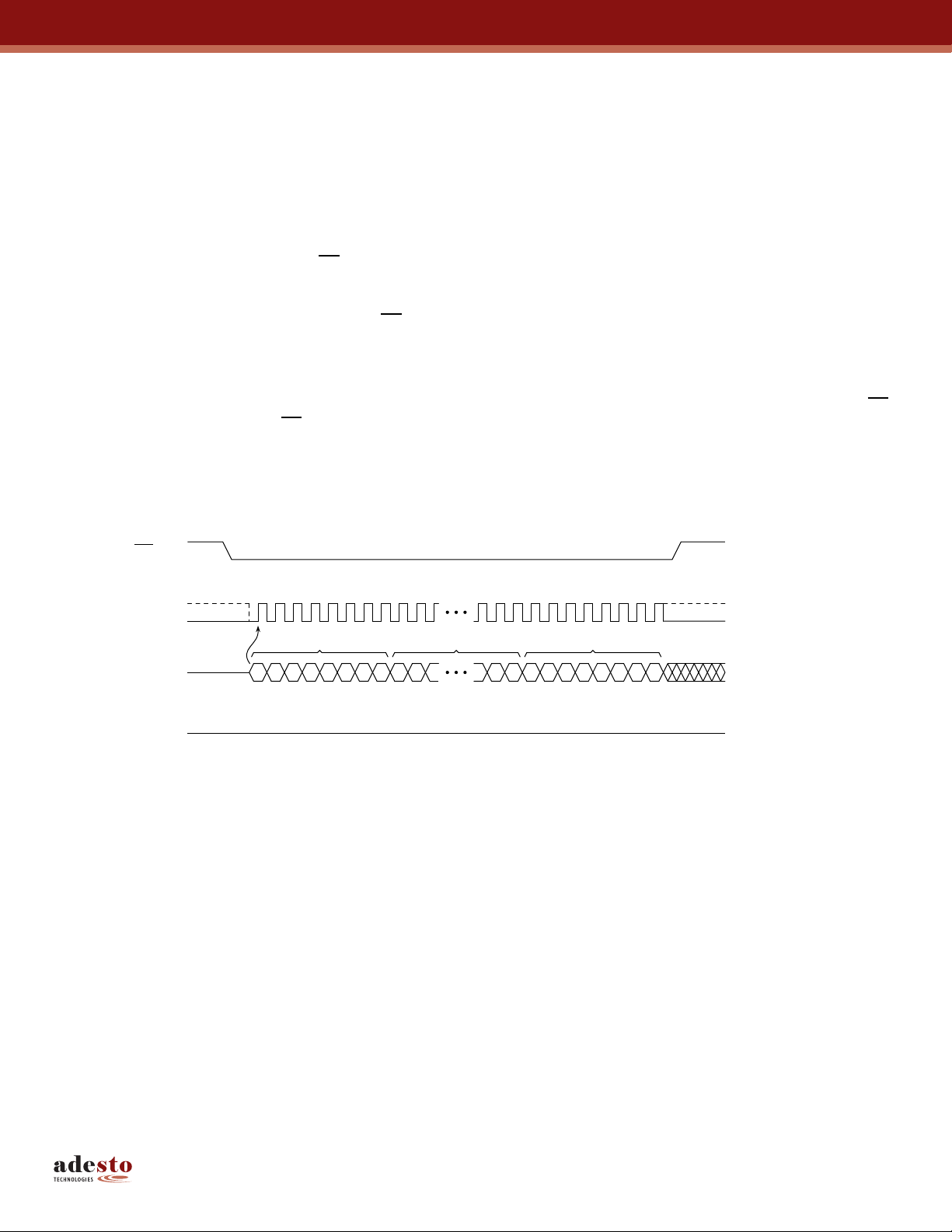
10.2 Freeze Sector Lockdown State
The current sector lockdown state can be permanently frozen so that no further modifications to the Sector Lockdown
Registers can be made; therefore, the Sector Lockdown command will be permanently disabled and no additional
sectors can be locked down aside from those already locked down. Any attempts to issue the Sector Lockdown
command after the sector lockdown state has been frozen will be ignored.
Before the Freeze Sector Lockdown State command can be issued, the Write Enable command must have been
previously issued to set the WEL bit in the Status Register to a Logical 1. In addition, the Sector Lockdown Enabled
(SLE) bit in the Status Register must have also been previously set to the Logical 1 state. To issue the Freeze Sector
Lockdown State command, the
followed by three command specific address bytes of 55AA40h. After the three address bytes have been clocked in, a
confirmation byte of D0h must be clocked in immediately following the three address bytes. Any additional data clocked
into the device will be ignored. When the
frozen within a time of t
LOCK
the SLE bit will be permanently reset to a Logical 0 to indicate that the Sector Lockdown command is permanently
disabled.
The complete and correct three address bytes and the confirmation byte must be clocked into the device before the
pin is deasserted and the
will abort the operation. When the device aborts the Freeze Sector Lockdown State operation, the WEL bit in the Status
Register will be reset to a Logical 0; however, the state of the SLE bit will be unchanged.
Figure 10-2. Freeze Sector Lockdown State
CS pin must first be asserted and the opcode of 34h must be clocked into the device
. In addition, the WEL bit in the Status Register will be reset back to the Logical 0 state and
CS pin must be deasserted on a byte boundary (multiples of eight bits); otherwise, the device
CS pin is deasserted, the current sector lockdown state will be permanently
CS
CS
SCK
SI
SO
2310
Opcode
00110100
MSB MSB
High-impedance
6754983937 3833 36353431 3229 30
Address Bits A23-A0 Confirmation Byte IN
01 0000
11010000
MSB
AT25DQ321 [DATASHEET]
8718D–DFLASH–12/2012
34
Page 35
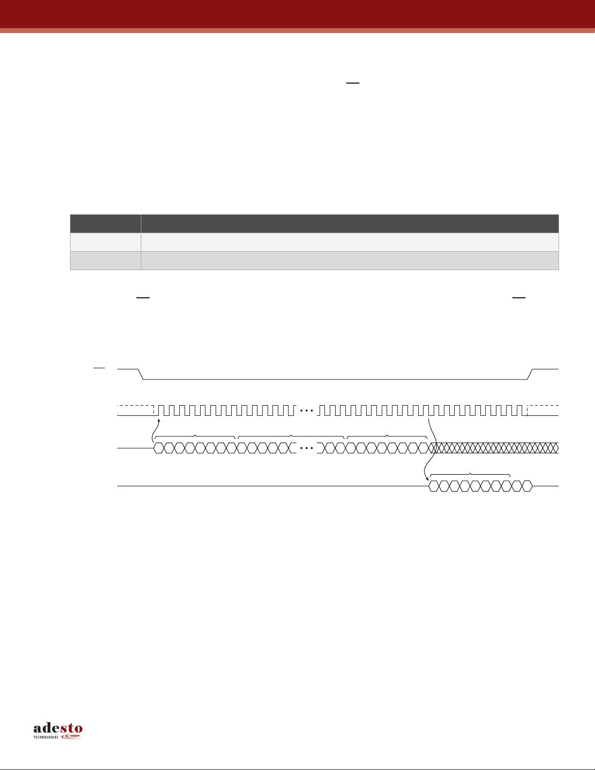
10.3 Read Sector Lockdown Registers
The Sector Lockdown Registers can be read to determine the current lockdown status of each physical 64KB sector. To
read the Sector Lockdown Register for a particular 64KB sector, the
must be clocked in. Once the opcode has been clocked in, three address bytes designating any address within the 64KB
sector must be clocked in. After the address bytes have been clocked in, data will be output on the SO pin during every
subsequent clock cycle. The data being output will be a repeating byte of either FFh or 00h to denote the value of the
appropriate Sector Lockdown Register.
At clock frequencies above f
above f
, at least two bytes of data must be clocked out from the device in order to determine the correct status of the
CLK
appropriate Sector Lockdown Register.
Table 10-2. Read Sector Lockdown Register - Output Data
Output Data Sector Lockdown Register Value
00h Sector Lockdown Register Value is 0 (Sector is Not Locked Down).
FFh Sector Lockdown Register Value is 1 (Sector is Permanently Locked Down).
Deasserting the CS pin will terminate the read operation and put the SO pin into a high-impedance state. The CS pin can
be deasserted at any time and does not require that a full byte of data be read.
, the first byte of data output will not be valid. Therefore, if operating at clock frequencies
CLK
CS pin must first be asserted and the opcode of 35h
Figure 10-3. Read Sector Lockdown Register
CS
2310
675410119812 394243414037 3833 36353431 3229 30 44 47 484645
SCK
Opcode
SI
SO
00110101
MSB MSB
High-impedance
AAAA AAAAA
Address Bits A23-A0 Don't Care
XXXXXXXX
MSB
Data Byte
DDDDDDDDDD
MSB MSB
AT25DQ321 [DATASHEET]
8718D–DFLASH–12/2012
35
Page 36

10.4 Program OTP Security Register
The device contains a specialized OTP (One-Time Programmable) Security Register that can be used for purposes such
as unique device serialization, system-level Electronic Serial Number (ESN) storage, locked key storage, etc. The OTP
Security Register is independent of the Main Flash Memory Array and is comprised of a total of 128 bytes of memory
divided into two portions. The first 64 bytes (byte locations 0 through 63) of the OTP Security Register are allocated as a
one-time user programmable space. Once these 64 bytes have been programmed, they cannot be erased or
reprogrammed. The remaining 64 bytes of the OTP Security Register (byte locations 64 through 127) are factory
programmed by Adesto
cannot be changed.
Table 10-3. OTP Security Register
0 1 . . . 62 63 64 65 . . . 126 127
One-Time User Programmable Factory Programmed by Adesto
The user-programmable portion of the OTP Security Register does not need to be erased before it is programmed. In
addition, the Program OTP Security Register command operates on the entire 64-byte user-programmable portion of the
OTP Security Register at one time. Once the user-programmable space has been programmed with any number of
bytes, the user-programmable space cannot be programmed again; therefore, it is not possible to only program the first
two bytes of the register and then program the remaining 62 bytes at a later time.
Before the Program OTP Security Register command can be issued, the Write Enable command must have been
previously issued to set the WEL bit in the Status Register to a Logical 1. To program the OTP Security Register, the
pin must first be asserted and an opcode of 9Bh must be clocked into the device followed by the three address bytes
denoting the first byte location of the OTP Security Register to begin programming at. Since the size of the
user-programmable portion of the OTP Security Register is 64 bytes, the upper order address bits do not need to be
decoded by the device, therefore, address bits A23-A6 will be ignored by the device and their values can be either a
Logical 1 or 0. After the address bytes have been clocked in, data can then be clocked into the device and will be stored
in the internal buffer.
If the starting memory address denoted by A23-A0 does not start at the beginning of the OTP Security Register memory
space (A5-A0 are not all 0), then special circumstances regarding which OTP Security Register locations to be
programmed will apply. In this situation, any data that is sent to the device that goes beyond the end of the 64-byte
user-programmable space will wrap around back to the beginning of the OTP Security Register.
®
and will contain a unique value for each device. The factory programmed data is fixed and
Security Register Byte Number
CS
Example: If the starting address denoted by A23-A0 is 00003Eh and three bytes of data are sent to the device, then
the first two bytes of data will be programmed at OTP Security Register addresses 00003Eh and 00003Fh
while the last byte of data will be programmed at address 000000h. The remaining bytes in the OTP
Security Register (addresses 000001h through 00003Dh) will not be programmed and will remain in the
erased state (FFh). In addition, if more than 64 bytes of data are sent to the device, then only the last
64 bytes sent will be latched into the internal buffer.
When the
CS pin is deasserted, the device will take the data stored in the internal buffer and program it into the
appropriate OTP Security Register locations based on the starting address specified by A23-A0 and the number of data
bytes sent to the device. If less than 64 bytes of data were sent to the device, then the remaining bytes within the OTP
Security Register will not be programmed and will remain in the erased state (FFh). The programming of the data bytes
is internally self-timed and should take place in a time of t
. It is not possible to suspend the programming of the OTP
OTPP
Security Register.
AT25DQ321 [DATASHEET]
8718D–DFLASH–12/2012
36
Page 37
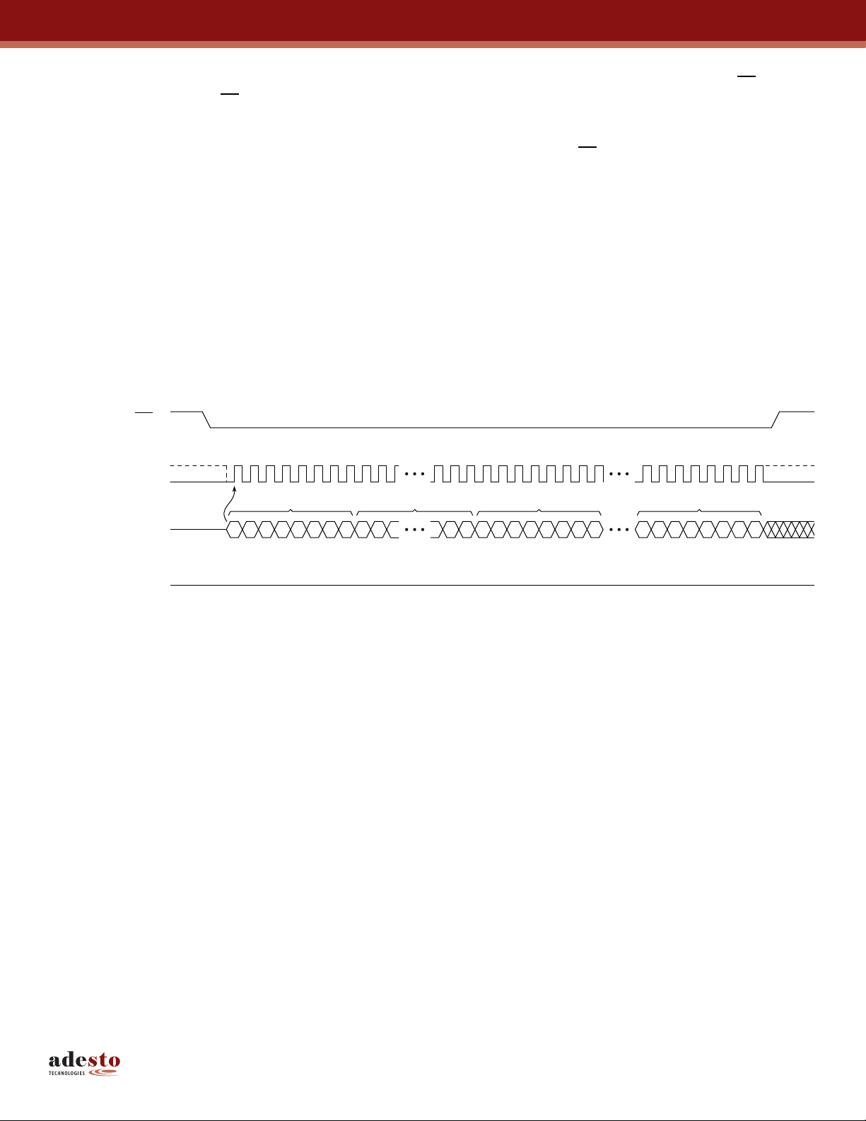
The three address bytes and at least one complete byte of data must be clocked into the device before the CS pin is
deasserted and the
CS pin must be deasserted on byte boundaries (multiples of eight bits); otherwise, the device will
abort the operation and the user-programmable portion of the OTP Security Register will not be programmed. The WEL
bit in the Status Register will be reset back to the Logical 0 state if the OTP Security Register program cycle aborts due
to an incomplete address being sent, an incomplete byte of data being sent, the
CS pin being deasserted on non-byte
boundaries or because the user-programmable portion of the OTP Security Register was previously programmed.
While the device is programming the OTP Security Register, the Status Register can be read and will indicate that the
device is busy. For faster throughput, it is recommended that the Status Register be polled rather than waiting the t
OTPP
time to determine if the data bytes have finished programming. At some point before the OTP Security Register
programming completes, the WEL bit in the Status Register will be reset back to the Logical 0 state.
If the device is powered-down during the OTP Security Register program cycle, then the contents of the 64-byte user
programmable portion of the OTP Security Register cannot be guaranteed and cannot be programmed again.
The Program OTP Security Register command utilizes the internal 256-buffer for processing. Therefore, the contents of
the buffer will be altered from its previous state when this command is issued.
Figure 10-4. Program OTP Security Register
CS
SCK
SI
SO
2310
Opcode
10011011
MSB MSB
High-impedance
6754983937 3833 36353431 3229 30
Address Bits A23-A0 Data In Byte 1
AA AAAA
DDDDDDDD
MSB
Data In Byte N
DDDDDDDD
MSB
AT25DQ321 [DATASHEET]
8718D–DFLASH–12/2012
37
Page 38

10.5 Read OTP Security Register
The OTP Security Register can be sequentially read in a similar fashion to the Read Array operation up to the maximum
clock frequency specified by f
of 77h must be clocked into the device. After the opcode has been clocked in, the three address bytes must be clocked in
to specify the starting address location of the first byte to read within the OTP Security Register. Following the three
address bytes, two dummy bytes must be clocked into the device before data can be output.
After the three address bytes and the dummy bytes have been clocked in, additional clock cycles will result in OTP
Security Register data being output on the SO pin. When the last byte (00007Fh) of the OTP Security Register has been
read, the device will continue reading back at the beginning of the register (000000h). No delays will be incurred when
wrapping around from the end of the register to the beginning of the register.
Deasserting the
CS pin will terminate the read operation and put the SO pin into a high-impedance state. The CS pin can
be deasserted at any time and does not require that a full byte of data be read.
Figure 10-5. Read OTP Security Register
CS
. To read the OTP Security Register, the CS pin must first be asserted and the opcode
MAX
SCK
SI
SO
2310
Opcode
01110111
MSB MSB
High-impedance
675410119812 3336353431 3229 30
Address Bits A23-A0
AAAA AAAAA XXX
XXXXXX
MSB
Don't Care
Data Byte 1
DDDDDDDDDD
MSB MSB
AT25DQ321 [DATASHEET]
8718D–DFLASH–12/2012
38
Page 39
11. Status Register Commands
11.1 Read Status Register
The 2-byte Status Register can be read to determine the device’s ready/busy status, as well as the status of many other
functions such as Hardware Locking and Software Protection. The Status Register can be read at any time, including
during an internally self-timed program or erase operation.
To read the Status Register, the
After the opcode has been clocked in, the device will begin outputting Status Register data on the SO pin during every
subsequent clock cycle. After the second byte of the Status Register has been clocked out, the sequence will repeat itself
starting again with the first byte of the Status Register as long as the
pulsed. The data in the Status Register is constantly being updated, so each repeating sequence will output new data.
The RDY/BSY status is available for both bytes of the Status Register and is updated for each byte.
At clock frequencies above f
operating at clock frequencies above f
the correct values of both bytes of the Status Register.
Deasserting the
state. The
Table 11-1. Status Register Format – Byte 1
(1)
Bit
CS pin will terminate the Read Status Register operation and put the SO pin into a high-impedance
CS pin can be deasserted at any time and does not require that a full byte of data be read.
CS pin must first be asserted and the opcode of 05h must be clocked into the device.
, the first two bytes of data output from the Status Register will not be valid. Therefore, if
CLK
, at least four bytes of data must be clocked out from the device in order to read
CLK
Name Type
CS pin remains asserted and the clock pin is being
(2)
Description
7 SPRL
6 RES Reserved for Future Use R 0 Reserved for future use.
5 EPE Erase/Program Error R
4 WPP Write Protect (WP) Pin Status R
3:2 SWP Software Protection Status R
1 WEL Write Enable Latch Status R
Sector Protection Registers
Locked
R/W
0 Sector Protection Registers are unlocked. (Default)
1 Sector Protection Registers are locked.
0 Erase or Program Operation was successful.
1 Erase or Program Error detected.
0 WP is asserted.
1 WP is deasserted.
All sectors are software unprotected.
00
(All Sector Protection Registers are 0)
Some sectors are software protected.
Read individual Sector Protection Registers to
01
determine which sectors are protected.
10 Reserved for future use.
All sectors are software protected.
11
(All Sector Protection Registers are 1 – Default)
0 Device is not write enabled. (Default)
1 Device is write enabled.
0 RDY/BSY Ready/Busy Status R
0 Device is ready.
1 Device is busy with an internal operation.
Notes: 1. Only bit 7 of Status Register Byte 1 will be modified when using the Write Status Register Byte 1 command.
2. R/W = Readable and writeable
R = Readable only
AT25DQ321 [DATASHEET]
8718D–DFLASH–12/2012
39
Page 40

Table 11-2. Status Register Format – Byte 2
(2)
Bit
7 RES Reserved for Future Use R 0 Reserved for future use.
6 RES Reserved for Future Use R 0 Reserved for future use.
5 RES Reserved for Future Use R 0 Reserved for future use.
Name Type
(2)
Description
4 RSTE Reset Enabled R/W
3 SLE Sector Lockdown Enabled R/W
2 PS Program Suspend Status R
1 ES Erase Suspend Status R
0 RDY/BSY Ready/Busy Status R
Notes: 1. Only bits 4 and 3 of Status Register Byte 2 will be modified when using the Write Status Register Byte 2
11.1.1 SPRL Bit
command.
2. R/W = Readable and Writeable
R = Readable only
0 Reset command is disabled. (Default)
1 Reset command is enabled.
Sector Lockdown and Freeze Sector Lockdown.
0
State commands are disabled.(Default)
Sector Lockdown and Freeze Sector Lockdown
1
State commands are enabled.
0 No sectors are program suspended. (Default)
1 A sector is program suspended.
0 No sectors are erase suspended. (Default)
1 A sector is erase suspended.
0 Device is ready.
1 Device is busy with an internal operation.
The SPRL bit is used to control whether the Sector Protection Registers can be modified or not. When the SPRL bit is in
the Logical 1 state, all Sector Protection Registers are locked and cannot be modified with the Protect Sector and
Unprotect Sector commands (the device will ignore these commands). In addition, the Global Protect and Global
Unprotect features cannot be performed. Any sectors that are presently protected will remain protected and any sectors
that are presently unprotected will remain unprotected.
When the SPRL bit is in the Logical 0 state, all Sector Protection Registers are unlocked and can be modified (the
Protect Sector and Unprotect Sector commands, as well as the Global Protect and Global Unprotect features, will be
processed as normal). The SPRL bit defaults to the Logical 0 state after device power-up. The Reset command has no
effect on the SPRL bit.
The SPRL bit can be modified freely whenever the
WP pin is deasserted. However, if the WP pin is asserted, then the
SPRL bit may only be changed from a Logical 0 (Sector Protection Registers are unlocked) to a Logical 1 (Sector
Protection Registers are locked). In order to reset the SPRL bit back to a Logical 0 using the Write Status Register
Byte 1 command, the
WP pin will have to first be deasserted.
The SPRL bit is the only bit of Status Register Byte 1 that can be user modified via the Write Status Register Byte 1
command.
AT25DQ321 [DATASHEET]
8718D–DFLASH–12/2012
40
Page 41

11.1.2 EPE Bit
The EPE bit indicates whether the last erase or program operation completed successfully or not. If at least one byte
during the erase or program operation did not erase or program properly, then the EPE bit will be set to the Logical 1
state. The EPE bit will not be set if an erase or program operation aborts for any reason such as an attempt to erase or
program a protected region or a locked down sector, an attempt to erase or program a suspended sector or if the WEL bit
is not set prior to an erase or program operation. The EPE bit will be updated after every erase and program operation.
11.1.3 WPP Bit
The WPP bit can be read to determine if the WP pin has been asserted or not.
11.1.4 SWP Bits
The SWP bits provide feedback on the software protection status for the device. There are three possible combinations
of the SWP bits that indicate whether none, some or all of the sectors have been protected using the Protect Sector
command or the Global Protect feature. If the SWP bits indicate that some of the sectors have been protected, then the
individual Sector Protection Registers can be read with the Read Sector Protection Registers command to determine
which sectors are in fact protected.
11.1.5 WEL Bit
The WEL bit indicates the current status of the internal Write Enable Latch. When the WEL bit is in the Logical 0 state,
the device will not accept any Byte/Page Program, Erase, Protect Sector, Unprotect Sector, Sector Lockdown, Freeze
Sector Lockdown State, Program OTP Security Register, Write Status Register, or Write Configuration Register
commands. The WEL bit defaults to the Logical 0 state after a device power-up or reset operation. In addition, the WEL
bit will be reset to the Logical 0 state automatically under the following conditions:
Write Disable operation completes successfully.
Write Status Register operation completes successfully or aborts.
Write Configuration Register operation completes successfully or aborts.
Protect Sector operation completes successfully or aborts.
Unprotect Sector operation completes successfully or aborts.
Sector Lockdown operation completes successfully or aborts.
Freeze Sector Lockdown State operation completes successfully or aborts.
Program OTP Security Register operation completes successfully or aborts.
Byte/Page Program operation completes successfully or aborts.
Block Erase operation completes successfully or aborts.
Chip Erase operation completes successfully or aborts.
Hold condition aborts.
If the WEL bit is in the Logical 1 state, it will not be reset to a Logical 0 if an operation aborts due to an incomplete or
unrecognized opcode being clocked into the device before the
CS pin is deasserted. In order for the WEL bit to be reset
when an operation aborts prematurely, the entire opcode for a Byte/Page Program, Erase, Protect Sector, Unprotect
Sector, Sector Lockdown, Freeze Sector Lockdown State, Program OTP Security Register, Write Status Register, or
Write Configuration Register command must have been clocked into the device.
AT25DQ321 [DATASHEET]
8718D–DFLASH–12/2012
41
Page 42

11.1.6 RSTE Bit
The RSTE bit is used to enable or disable the Reset command. When the RSTE bit is in the Logical 0 state (the default
state after power-up), the Reset command is disabled and any attempts to reset the device using the Reset command
will be ignored. When the RSTE bit is in the Logical 1 state, the Reset command is enabled.
The RSTE bit will retain its state as long as power is applied to the device. Once set to the Logical 1 state, the RSTE bit
will remain in that state until it is modified using the Write Status Register Byte 2 command or until the device has been
power cycled. The Reset command itself will not change the state of the RSTE bit.
11.1.7 SLE Bit
The SLE bit is used to enable and disable the Sector Lockdown and Freeze Sector Lockdown State commands. When
the SLE bit is in the Logical 0 state (the default state after power-up), the Sector Lockdown and Freeze Sector Lockdown
commands are disabled. If the Sector Lockdown and Freeze Sector Lockdown commands are disabled, then any
attempts to issue the commands will be ignored. This provides a safeguard for these commands against accidental or
erroneous execution. When the SLE bit is in the Logical 1 state, the Sector Lockdown and Freeze Sector Lockdown
State commands are enabled.
Unlike the WEL bit, the SLE bit does not automatically reset after certain device operations. Therefore, once set, the SLE
bit will remain in the Logical 1 state until it is modified using the Write Status Register Byte 2 command or until the device
has been power cycled. The Reset command has no effect on the SLE bit.
If the Freeze Sector Lockdown State command has been issued, then the SLE bit will be permanently reset in the
Logical 0 state to indicate that the Sector Lockdown command has been disabled.
11.1.8 PS Bit
The PS bit indicates whether or not a sector is in the Program Suspend state.
11.1.9 ES Bit
The ES bit indicates whether or not a sector is in the Erase Suspend state.
11.1.10 RDY/BSY Bit
The RDY/BSY bit is used to determine whether or not an internal operation, such as a program or erase, is in progress.
To poll the RDY/BSY bit to detect the completion of a program or erase cycle, new Status Register data must be
continually clocked out of the device until the state of the RDY/BSY bit changes from a Logical 1 to a Logical 0.
Figure 11-1. Read Status Register
CS
SCK
SI
SO
2310
Opcode
00000101
MSB
High-impedance
675410119812 212217 20191815 1613 14 23 24 28 29272625 30
Status Register
Byte 1
DDDDDD DDDD
MSB MSB
Status Register
Byte 2
DDDDDDDD D DDD D D
MSB
Status Register
Byte 1
AT25DQ321 [DATASHEET]
8718D–DFLASH–12/2012
42
Page 43

11.2 Write Status Register Byte 1
The Write Status Register Byte 1 command is used to modify the SPRL bit of the Status Register and/or to perform a
Global Protect or Global Unprotect operation. Before the Write Status Register Byte 1 command can be issued, the Write
Enable command must have been previously issued to set the WEL bit in the Status Register to a Logical 1.
To issue the Write Status Register Byte 1 command, the
clocked into the device followed by one byte of data. The one byte of data consists of the SPRL bit value, a don’t care bit,
four data bits to denote whether a Global Protect or Unprotect should be performed and two additional don’t care bits
(see Table 11-3). Any additional data bytes that are sent to the device will be ignored. When the
the SPRL bit in the Status Register will be modified and the WEL bit in the Status Register will be reset back to a
Logical 0. The values of bits 5, 4, 3, and 2 and the state of the SPRL bit before the Write Status Register Byte 1
command was executed (the prior state of the SPRL bit) will determine whether or not a Global Protect or Global
Unprotect will be performed. See “Global Protect/Unprotect” on page 28 for more details.
The complete one byte of data must be clocked into the device before the CS pin is deasserted and the CS pin must be
deasserted on even byte boundaries (multiples of eight bits); otherwise, the device will abort the operation, the state of
the SPRL bit will not change, no potential Global Protect or Unprotect will be performed, and the WEL bit in the Status
Register will be reset back to the Logical 0 state.
If the
WP pin is asserted, then the SPRL bit can only be set to a Logical 1. If an attempt is made to reset the SPRL bit to
a Logical 0 while the
in the Status Register will be reset back to the Logical 0 state. In order to reset the SPRL bit to a Logical 0, the
must be deasserted.
Table 11-3. Write Status Register Byte 1 Format
WP pin is asserted, then the Write Status Register Byte 1 command will be ignored and the WEL bit
CS pin must first be asserted and the opcode of 01h must be
CS pin is deasserted,
WP pin
Bit 7 Bit 6 Bit 5 Bit 4 Bit 3 Bit 2 Bit 1 Bit 0
SPRL X Global Protect/Unprotect X X
Figure 11-2. Write Status Register Byte 1
CS
2310
6754
10 119814151312
SCK
Status Register IN
Byte 1
1
DXDDDDXX
MSB
SI
SO
Opcode
0000000
MSB
High-impedance
AT25DQ321 [DATASHEET]
8718D–DFLASH–12/2012
43
Page 44

11.3 Write Status Register Byte 2
The Write Status Register Byte 2 command is used to modify the RSTE and SLE bits of the Status Register. Using the
Write Status Register Byte 2 command is the only way to modify the RSTE and SLE bits in the Status Register during
normal device operation and the SLE bit can only be modified if the sector lockdown state has not been frozen. Before
the Write Status Register Byte 2 command can be issued, the Write Enable command must have been previously issued
to set the WEL bit in the Status Register to a Logical 1.
To issue the Write Status Register Byte 2 command, the CS pin must first be asserted and the opcode of 31h must be
clocked into the device followed by one byte of data. The one byte of data consists of three don’t care bits, the RSTE bit
value, the SLE bit value and three additional don’t care bits (see Table 11-4). Any additional data bytes that are sent to
the device will be ignored. When the
and the WEL bit in the Status Register will be reset back to a Logical 0. The SLE bit will only be modified if the Freeze
Sector Lockdown State command has not been previously issued.
The complete one byte of data must be clocked into the device before the
deasserted on even byte boundaries (multiples of eight bits); otherwise, the device will abort the operation, the state of
the RSTE and SLE bits will not change and the WEL bit in the Status Register will be reset back to the Logical 0 state.
Table 11-4. Write Status Register Byte 2 Format
Bit 7 Bit 6 Bit 5 Bit 4 Bit 3 Bit 2 Bit 1 Bit 0
X X X RSTE SLE X X X
CS pin is deasserted, the RSTE and SLE bits in the Status Register will be modified
CS pin is deasserted and the CS pin must be
Figure 11-3. Write Status Register Byte 2
CS
2310
6754
SCK
Opcode
SI
SO
0011000
MSB
High-impedance
10 119814151312
Status Register IN
Byte 2
1
XXXDDXXX
MSB
AT25DQ321 [DATASHEET]
8718D–DFLASH–12/2012
44
Page 45

11.4 Read Configuration Register
The non-volatile Configuration Register can be read to determine if the Quad-Input Byte/Page Program and Quad-Output
Read Array commands have been enabled. Unlike the Status Register, the Configuration Register can only be read
when the device is in an idle state (when the RDY/BSY bit of the Status Register indicates that the device is in a ready
state).
To read the Configuration Register, the
device. After the opcode has been clocked in, the device will begin outputting the one byte of Configuration Register
data on the SO pin during subsequent clock cycles. The data being output will be a repeating byte as long as the
remains asserted and the clock pin is being pulsed.
At clock frequencies above f
above f
, at least two bytes of data must be clocked out from the device in order to determine the correct value of the
CLK
Configuration Register.
Deasserting the
CS pin will terminate the Read Configuration Register operation and put the SO pin into a
high-impedance state. The
The Configuration Register is a non-volatile register; therefore, the contents of the Configuration Register are not
affected by power cycles or power-on reset operations.
Table 11-5. Configuration Register Format
, the first byte of data output will not be valid. Therefore, if operating at clock frequencies
CLK
CS pin can be deasserted at any time and does not require that a full byte of data be read.
CS pin must first be asserted and the opcode of 3Fh must be clocked into the
CS pin
(1)
Bit
Name Type
7 QE Quad Enable R/W
6:0 RES Reserved for Future Use R 0 Reserved for future use.
(2)
Description
0 Quad-Input/Output commands and operation disabled.
Quad-Input/Output commands and operation enabled.
1
(
WP and HOLD disabled)
Notes: 1. Only bit 7 of the Configuration Register will be modified when using the Write Configuration Register
command.
2. R/W = Readable and Writeable
R = Readable only
AT25DQ321 [DATASHEET]
8718D–DFLASH–12/2012
45
Page 46

11.4.1 QE Bit
The QE bit is used to control whether the Quad-Input Byte/Page Program and Quad-Output Read Array commands are
enabled or disabled. When the QE bit is in the Logical 1 state, the Quad-Input Byte/Page Program and Quad-Output
Read Array commands are enabled and will be recognized by the device. In addition, the
disabled and the
is I/O
3
When the QE bit is in the Logical 0 state, the Quad-Input Byte/Page Program and Quad-Output Read Array commands
are disabled and will not be recognized by the device as valid commands and the
control pins. The
The Reset command has no effect on the QE bit. The QE bit defaults to the Logical 0 state when devices are initially
shipped from Adesto.
Figure 11-4. Read Configuration Register
WP and HOLD functions are
WP and HOLD pins themselves operate as a bidirectional input/output pins (WP is I/O2 and HOLD
).
WP and HOLD pins function as normal
WP and HOLD pins should be externally pulled-high to avoid erroneous or unwanted device operation.
CS
SCK
SI
SO
2310
Opcode
00111111
MSB
High-impedance
675410119812 212217 20191815 1613 14 23 24
Configuration
Register Out
XXXXXX DXXD
MSB MSB
MSB
Configuration
Register Out
XXXXXXXD
AT25DQ321 [DATASHEET]
8718D–DFLASH–12/2012
46
Page 47

11.5 Write Configuration Register
The Write Configuration Register command is used to modify the QE bit of the non-volatile Configuration Register.
Before the Write Configuration Register command can be issued, the Write Enable command must have been previously
issued to set the WEL bit in the Status Register to a Logical 1.
To issue the Write Configuration Register command, the
clocked into the device followed by one byte of data. The one byte of data consists of the QE bit value and seven don’t
care bits (Table 11-6). Any additional data clocked into the device will be ignored. When the
QE bit of the Configuration Register will be modified within a time of t
reset back to a Logical 0.
The complete one byte of data must be clocked into the device before the
deasserted on byte boundaries (multiples of eight bits); otherwise, the device will abort the operation, the value of the
Configuration Register will not change and the WEL bit in the Status Register will be reset back to the Logical 0 state.
The Configuration Register is a non-volatile register and is subject to the same program/erase endurance characteristics
of the Main Memory Array.
The programming of the Configuration Register is internally self-timed and should take place in a time of t
Configuration Register is being updated, the Status Register can be read and will indicate that the device is busy. For
faster throughput, it is recommended that the Status Register be polled rather than waiting the t
the Configuration Register has completed the programming cycle. At some point before the programming cycle
completes, the WEL bit in the Status Register will be reset back to the Logical 0 state.
Table 11-6. Write Configuration Register Format
CS pin must first be asserted and the opcode of 3Eh must be
CS pin is deasserted, the
and the WEL bit in the Status Register will be
WRCR
CS pin is deasserted and the CS pin must be
While the
WRCR.
time to determine if
WRCR
Bit 7 Bit 6 Bit 5 Bit 4 Bit 3 Bit 2 Bit 1 Bit 0
QE X X X X X X X
Figure 11-5. Write Configuration Register
CS
2310
6754
10 119814151312
SCK
Configuration
Register IN
DXXXXXXX
MSB
SI
SO
Opcode
0011111
MSB
High-impedance
0
AT25DQ321 [DATASHEET]
8718D–DFLASH–12/2012
47
Page 48

12. Other Commands and Functions
12.1 Reset
In some applications, it may be necessary to prematurely terminate a program or erase cycle early rather than wait the
hundreds of microseconds or milliseconds necessary for the program or erase operation to complete normally. The
Reset command allows a program or erase operation in progress to be ended abruptly and returns the device to an idle
state. Since the need to reset the device is immediate, the Write Enable command does not need to be issued prior to the
Reset command being issued. Therefore, the Reset command operates independently of the state of the WEL bit in the
Status Register.
The Reset command can only be executed if the command has been enabled by setting the Reset Enabled (RSTE) bit in
the Status Register to a Logical 1. If the Reset command has not been enabled (the RSTE bit is in the Logical 0 state),
then any attempts at executing the Reset command will be ignored.
To perform a Reset, the
address bytes need to be clocked in, but a confirmation byte of D0h must be clocked into the device immediately after the
opcode. Any additional data clocked into the device after the confirmation byte will be ignored. When the
deasserted, the program or erase operation currently in progress will be terminated within a time of t
program or erase operation may not complete before the device is reset, the contents of the page being programmed or
the block being erased cannot be guaranteed to be valid.
The Reset command has no effect on the states of the Sector Protection Registers, the Sector Lockdown Registers, the
Configuration Register or the SPRL, RSTE, and SLE bits in the Status Register. The WEL, PS and ES bits of the Status
Register, however, will be reset back to their default states. If a Reset operation is performed while a sector is erase
suspended, the suspend operation will abort and the contents of the block being erased in the suspended sector will be
left in an undefined state. If a Reset is performed while a sector is program suspended, the suspend operation will abort
and the contents of the page that was being programmed and subsequently suspended will be undefined. The remaining
pages in the 64KB sector will retain their previous contents.
The complete opcode and confirmation byte must be clocked into the device before the CS pin is deasserted and the CS
pin must be deasserted on a byte boundary (multiples of eight bits); otherwise, no Reset operation will be performed.
CS pin must first be asserted and the opcode of F0h must be clocked into the device. No
CS pin is
. Since the
RST
Figure 12-1. Reset
CS
SCK
SI
SO
2310
Opcode Confirmation Byte IN
1111000
MSB
High-impedance
6754
0
10 119814151312
11010000
MSB
AT25DQ321 [DATASHEET]
8718D–DFLASH–12/2012
48
Page 49

12.2 Read Manufacturer and Device ID
Identification information can be read from the device to enable systems to electronically query and identify the device
while it is in system. The identification method and the command opcode comply with the JEDEC standard for
“Manufacturer and Device ID Read Methodology for SPI Compatible Serial Interface Memory Devices”. The type of
information that can be read from the device includes the JEDEC Defined Manufacturer ID, the vendor specific Device ID
and the vendor specific Extended Device Information.
The Read Manufacturer and Device ID command is limited to a maximum clock frequency of f
devices are capable of operating at very high clock frequencies, applications should be designed to read the
identification information from the devices at a reasonably low clock frequency to ensure that all devices to be used in the
application can be identified properly. Once the identification process is complete, the application can then increase the
clock frequency to accommodate specific Flash devices that are capable of operating at the higher clock frequencies.
To read the identification information, the CS pin must first be asserted and the opcode of 9Fh must be clocked into the
device. After the opcode has been clocked in, the device will begin outputting the identification data on the SO pin during
the subsequent clock cycles. The first byte that will be output will be the Manufacturer ID followed by two bytes of Device
ID information. The fourth byte output will be the Extended Device Information (EDI) String Length, which will be 01h
indicating that one byte of EDI data follows. After the one byte of EDI data is output, the SO pin will go into a
high-impedance state; therefore, additional clock cycles will have no affect on the SO pin and no data will be output. As
indicated in the JEDEC standard, reading the EDI String Length and any subsequent data is optional.
Deasserting the
high-impedance state. The
Table 12-1. Manufacturer and Device ID Information
CS pin will terminate the Manufacturer and Device ID Read operation and put the SO pin into a
CS pin can be deasserted at any time and does not require that a full byte of data be read.
. Since not all Flash
CLK
Byte No. Data Type Value
1 Manufacturer ID 1Fh
2 Device ID (Part 1) 87h
3 Device ID (Part 2) 00h
4 [Optional to Read] Extended Device Information (EDI) String Length 01h
5 [Optional to Read] EDI Byte 1 00h
Table 12-2. Manufacturer and Device ID Details
Hex
Data Type Bit 7 Bit 6 Bit 5 Bit 4 Bit 3 Bit 2 Bit 1 Bit 0
JEDEC Assigned Code
Manufacturer ID
0 0 0 1 1 1 1 1
Family Code Density Code
Device ID (Part 1)
1 0 0 0 0 1 1 1
Sub Code Product Variant
Device ID (Part 2)
0 0 0 0 0 0 0 0
Value Details
1Fh JEDEC Code: 0001 1111 (1Fh for Adesto)
Family Code: 100 (Quad-I/O or Rapid4™)
87h
Density Code: 00111 (32-Mbit)
Sub Code: 000 (Quad-I/O Series)
00h
Product Variant: 00000 (Standard Version)
Table 12-3. EDI Data
Byte Number Bit 7 Bit 6 Bit 5 Bit 4 Bit 3 Bit 2 Bit 1 Bit 0
RFU Device Revision
1
0 0 0 0 0 0 0 0
Hex
Value Details
RFU: Reserved for Future Use
00h
Density Code: 00000 (Initial Version)
AT25DQ321 [DATASHEET]
8718D–DFLASH–12/2012
49
Page 50
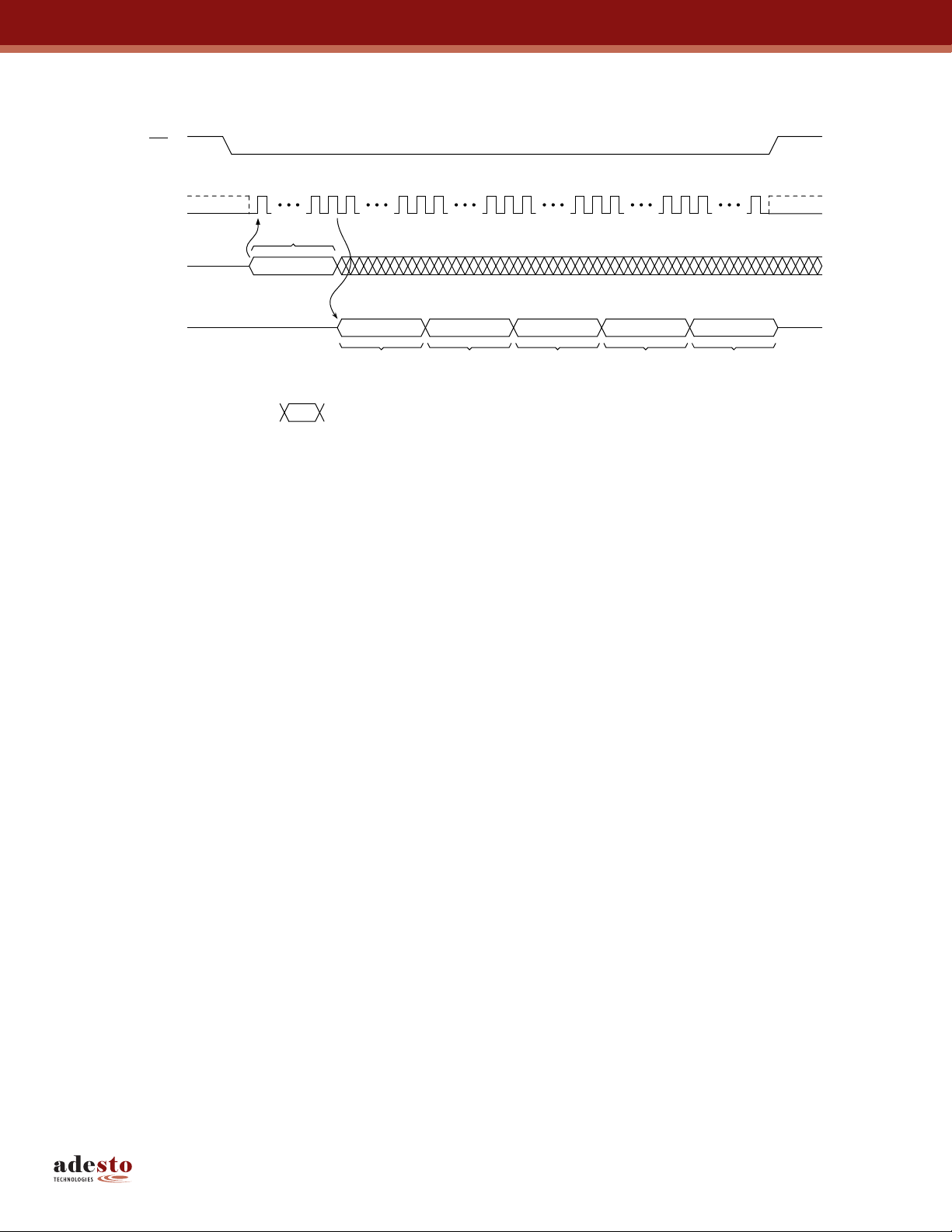
Figure 12-2. Read Manufacturer and Device ID
CS
60
87 46
14 1615 22 2423 38 403930 3231
SCK
Opcode
SI
SO
High-impedance
9Fh
1Fh 86h 00h 01h 00h
Manufacturer ID Device ID
Byte 1
Device ID
Byte 2
String Length
Note: Each transition shown for SI and SO represents one byte (8 bits)
EDI
EDI
Data Byte 1
AT25DQ321 [DATASHEET]
8718D–DFLASH–12/2012
50
Page 51
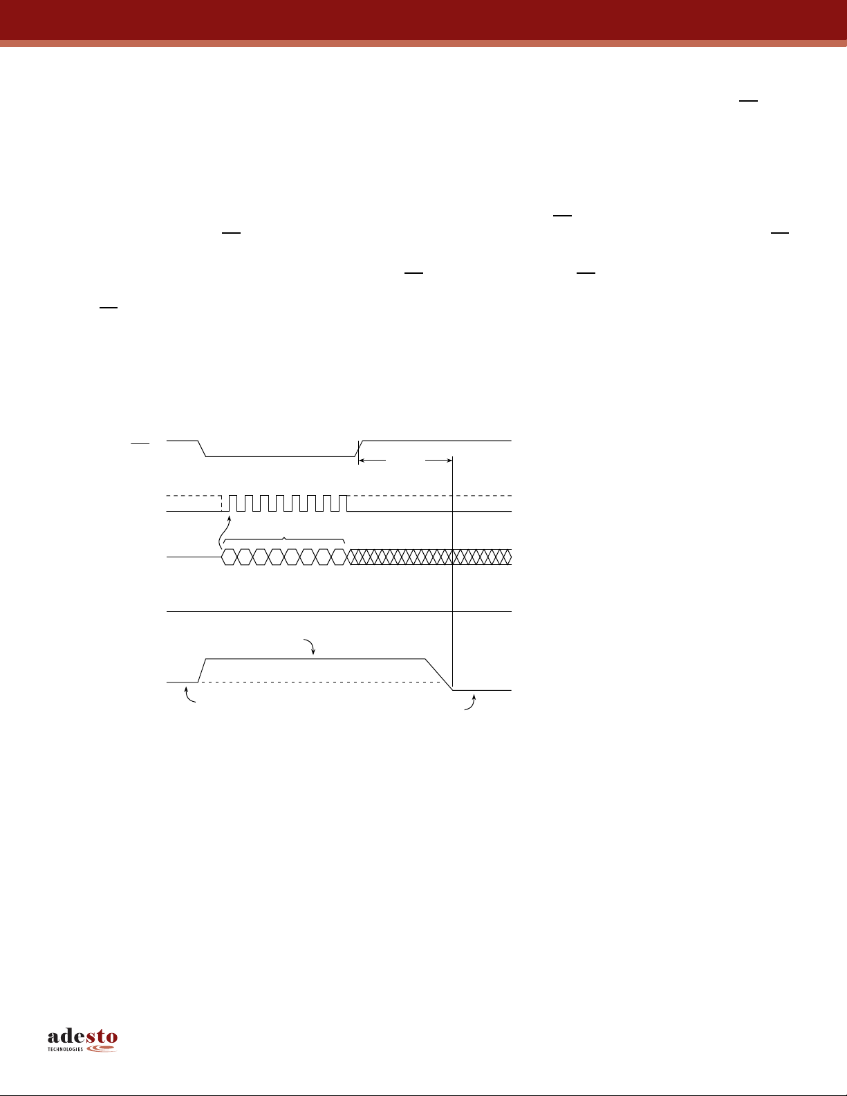
12.3 Deep Power-Down
During normal operation, the device will be placed in the standby mode to consume less power as long as the CS pin
remains deasserted and no internal operation is in progress. The Deep Power-Down command offers the ability to place
the device into an even lower power consumption state called the Deep Power-Down mode.
When the device is in the Deep Power-Down mode, all commands including the Read Status Register command will be
ignored with the exception of the Resume from Deep Power-Down command. Since all commands will be ignored, the
mode can be used as an extra protection mechanism against program and erase operations.
Entering the Deep Power-Down mode is accomplished by simply asserting the
then deasserting the
pin is deasserted, the device will enter the Deep Power-Down mode within the maximum time of t
The complete opcode must be clocked in before the
boundary (multiples of eight bits); otherwise, the device will abort the operation and return to the standby mode once the
CS pin is deasserted. In addition, the device will default to the standby mode after a power-cycle.
The Deep Power-Down command will be ignored if an internally self-timed operation such as a program or erase cycle is
in progress. The Deep Power-Down command must be reissued after the internally self-timed operation has been
completed in order for the device to enter the Deep Power-Down mode.
Figure 12-3. Deep Power-Down
CS pin. Any additional data clocked into the device after the opcode will be ignored. When the CS
CS pin, clocking in the opcode of B9h and
.
EDPD
CS pin is deasserted and the CS pin must be deasserted on a byte
CS
SCK
SI
SO
I
CC
2310
Opcode
10111001
MSB
High-impedance
Active Current
Standby Mode Current
t
EDPD
6754
Deep Power-down Mode Current
AT25DQ321 [DATASHEET]
8718D–DFLASH–12/2012
51
Page 52
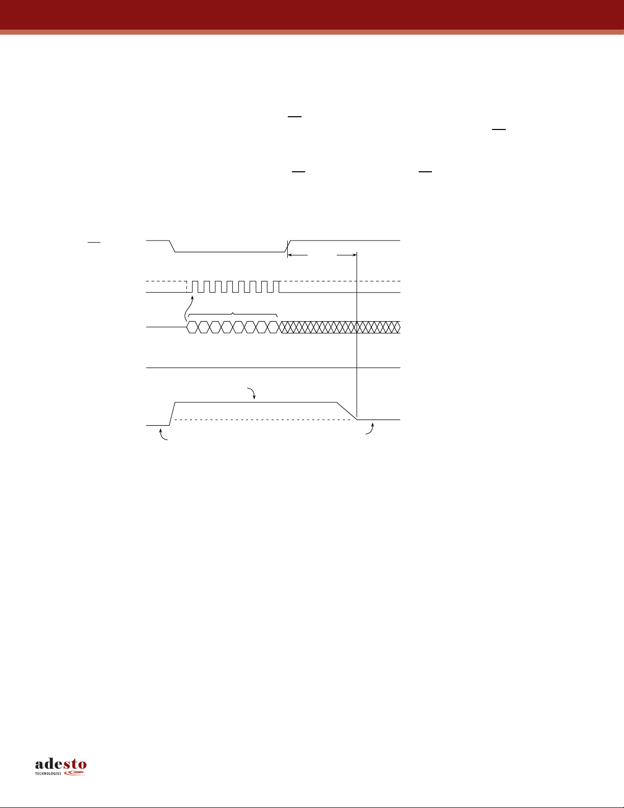
12.4 Resume from Deep Power-Down
In order to exit the Deep Power-Down mode and resume normal device operation, the Resume from Deep Power-Down
command must be issued. The Resume from Deep Power-Down command is the only command that the device will
recognized while in the Deep Power-Down mode.
To resume from the Deep Power-Down mode, the
the device. Any additional data clocked into the device after the opcode will be ignored. When the
the device will exit the Deep Power-Down mode within the maximum time of t
the device has returned to the standby mode, normal command operations such as Read Array can be resumed.
If the complete opcode is not clocked in before the
boundary (multiples of eight bits), then the device will abort the operation and return to the Deep Power-Down mode.
Figure 12-4. Resume from Deep Power-Down
CS pin must first be asserted and opcode of ABh must be clocked into
CS pin is deasserted,
and return to the standby mode. After
RDPD
CS pin is deasserted or if the CS pin is not deasserted on a byte
CS
SCK
SI
SO
I
CC
2310
Opcode
10101011
MSB
High-impedance
Active Current
Deep Power-down Mode Current
6754
t
RDPD
Standby Mode Current
AT25DQ321 [DATASHEET]
8718D–DFLASH–12/2012
52
Page 53

12.5 Hold
The HOLD pin is used to pause the serial communication with the device without having to stop or reset the clock
sequence. The Hold mode, however, does not have an affect on any internally self-timed operations such as a program
or erase cycle. Therefore, if an erase cycle is in progress, asserting the
erase cycle will continue until it is finished.
The Hold mode can only be entered while the
HOLD pin during the SCK low pulse. If the HOLD pin is asserted during the SCK high pulse, then the Hold mode won’t be
started until the beginning of the next SCK low pulse. The device will remain in the Hold mode as long as the
CS pin are asserted.
and
While in the Hold mode, the SO pin will be in a high-impedance state. In addition, both the SI pin and the SCK pin will be
ignored. The
To end the Hold mode and resume serial communication, the
HOLD pin is deasserted during the SCK high pulse, then the Hold mode won’t end until the beginning of the next SCK
the
low pulse.
If the
aborted and the device will reset the WEL bit in the Status Register back to the Logical 0 state.
Figure 12-5. Hold Mode
HOLD pin will not pause the operation and the
CS pin is asserted. The Hold mode is activated simply by asserting the
HOLD pin
WP pin, however, can still be asserted or deasserted while in the Hold mode.
HOLD pin must be deasserted during the SCK low pulse. If
CS pin is deasserted while the HOLD pin is still asserted, then any operation that may have been started will be
CS
SCK
HOLD
Hold HoldHold
AT25DQ321 [DATASHEET]
8718D–DFLASH–12/2012
53
Page 54
13. Electrical Specifications
13.1 Absolute Maximum Ratings*
Temperature under Bias . . . . . . . . . . -55C to +125C
Storage Temperature . . . . . . . . . . . . -65C to +150C
All Input Voltages (including NC Pins)
with Respect to Ground . . . . . . . . . . . . .-0.6V to +4.1V
All Output Voltages
with Respect to Ground . . . . . . . . .-0.6V to V
13.2 DC and AC Operating Range
Operating Temperature (Case) Industrial -40C to 85C
VCC Power Supply 2.7V to 3.6V
13.3 DC Characteristics
Symbol Parameter Condition Min Typ Max Units
I
SB
I
DPD
I
CC1
I
CC2
I
CC3
I
LI
I
LO
V
V
V
V
IL
IH
OL
OH
Standby Current
Deep Power-Down Current
Active Current, Read Operation
Active Current, Program Operation CS = VCC, VCC = Max 10 20 mA
Active Current, Erase Operation CS = VCC, VCC = Max 12 20 mA
Input Leakage Current VIN = CMOS levels 1 μA
Output Leakage Current V
Input Low Voltage 0.3 x V
Input High Voltage 0.7 x V
Output Low Voltage IOL = 1.6mA; VCC = Min 0.4 V
Output High Voltage IOH = -100μA; VCC = Min VCC - 0.2V V
*Notice: Stresses beyond those listed under “Absolute Maximum
+ 0.5V
CC
CS, WP, HOLD = VCC,
All inputs at CMOS levels
CS, WP, HOLD = VCC,
All inputs at CMOS levels
f = 100 MHz; I
CS = VIL, VCC = Max
f = 85 MHz; I
OUT
CS = VIL, VCC = Max
f = 66 MHz; I
OUT
CS = VIL, VCC = Max
f = 50 MHz; I
OUT
CS = VIL, VCC = Max
f = 33 MHz; I
OUT
CS = VIL, VCC = Max
f = 20 MHz; I
OUT
CS = VIL, VCC = Max
= CMOS levels 1 μA
OUT
Ratings” may cause permanent damage to the device.
Functional operation of the device at these ratings or any
other conditions beyond those indicated in the operational
sections of this specification is not implied. Exposure to
absolute maximum rating conditions for extended periods
may affect device reliability. Voltage extremes referenced in
the "Absolute Maximum Ratings" are intended to
accommodate short duration undershoot/overshoot
conditions and does not imply or guarantee functional device
operation at these levels for any extended period of time.
AT25DQ321
25 50 μA
5 10 μA
= 0mA;
OUT
= 0mA;
= 0mA;
= 0mA;
= 0mA;
= 0mA;
CC
12 19
10 17
8 14
7 12
6 10
5 8
CC
mA
V
V
AT25DQ321 [DATASHEET]
8718D–DFLASH–12/2012
54
Page 55
13.4 AC Characteristics – Maximum Clock Frequencies
Symbol Parameter Min Max Units
RapidS and SPI Operation
f
MAX
f
CLK
f
RDLF
f
RDDO
f
RDQO
Maximum Clock Frequency for All Operations – RapidS Operation Only
(Excluding 03h, 0Bh, 3Bh, 6Bh, and 9F Opcodes)
Maximum Clock Frequency for All Operations (Excluding 03h Opcode) 85 MHz
Maximum Clock Frequency for 03h Opcode (Read Array – Low Frequency) 50 MHz
Maximum Clock Frequency for 3Bh Opcode (Dual-Output Read) 85 MHz
Maximum Clock Frequency for 6Bh Opcode (Quad-Output Read) 66 MHz
13.5 AC Characteristics – All Other Parameters
Symbol Parameter Min Max Units
t
CLKH
t
CLKL
t
CLKR
t
CLKF
t
CSH
t
CSLS
t
CSLH
t
CSHS
t
CSHH
t
DS
t
DH
(1)
t
DIS
(2)
t
V
t
OH
t
HLS
t
HLH
t
HHS
t
HHH
t
HLQZ
t
HHQX
(1)(3)
t
WPS
(1)(3)
t
WPH
t
SECP
t
SECUP
t
LOCK
t
EDPD
t
RDPD
t
RST
Notes: 1. Not 100% tested. (Value guaranteed by design and characterization)
Clock High Time 4.3 ns
Clock Low Time 4.3 ns
(1)
Clock Rise Time, Peak-to-Peak (Slew Rate) 0.1 V/ns
(1)
Clock Fall Time, Peak-to-Peak (Slew Rate) 0.1 V/ns
Chip Select High Time 50 ns
Chip Select Low Setup Time (Relative to Clock) 5 ns
Chip Select Low Hold Time (Relative to Clock) 5 ns
Chip Select High Setup Time (Relative to Clock) 5 ns
Chip Select High Hold Time (Relative to Clock) 5 ns
Data In Setup Time 2 ns
Data In Hold Time 1 ns
Output Disable Time 5 ns
Output Valid Time 5 ns
Output Hold Time 2 ns
HOLD Low Setup Time (Relative to Clock) 5 ns
HOLD Low Hold Time (Relative to Clock) 5 ns
HOLD High Setup Time (Relative to Clock) 5 ns
HOLD High Hold Time (Relative to Clock) 5 ns
(1)
HOLD Low to Output High-Z 5 ns
(1)
HOLD High to Output Low-Z 5 ns
Write Protect Setup Time 20 ns
Write Protect Hold Time 100 ns
(1)
Sector Protect Time (From Chip Select High) 20 ns
(1)
Sector Unprotect Time (From Chip Select High) 20 ns
(1)
Sector Lockdown and Freeze Sector Lockdown State Time (From Chip Select High) 200 μs
(1)
Chip Select High to Deep Power-Down 1 μs
(1)
Chip Select High to Standby Mode 30 μs
Reset Time 30 μs
2. 15pF load at frequencies above 70MHz, 30pF otherwise.
3. Only applicable as a constraint for the Write Status Register Byte 1 command when SPRL = 1.
100 MHz
AT25DQ321 [DATASHEET]
8718D–DFLASH–12/2012
55
Page 56
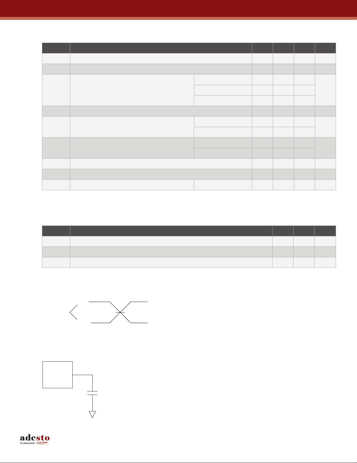
13.6 Program and Erase Characteristics
Symbol Parameter Min Typ Max Units
(1)
t
PP
t
BP
t
BLKE
t
CHPE
t
SUSP
Page Program Time (256-bytes) 1.5 3.0 ms
Byte Program Time 7 μs
(1)
Block Erase Time
(1)(2)
Chip Erase Time 25 40 sec
Suspend Time
4KB 50 200
ms32KB 250 600
64KB 400 950
Program 10 20
μs
Erase 25 40
t
RES
t
OTPP
t
WRSR
t
WRCR
Resume Time
(1)
OTP Security Register Program Time 200 500 μs
(2)
Write Status Register Time 200 ns
Write Configuration Register Time 15 35 ms
Notes: 1. Maximum values indicate worst-case performance after 100,000 erase/program cycles.
2. Not 100% tested. (Value guaranteed by design and characterization)
13.7 Power-up Conditions
Symbol Parameter Min Max Units
t
VCSL
t
PUW
V
POR
Minimum VCC to Chip Select Low Time 70 μs
Power-Up Device Delay Before Program or Erase Allowed 10 ms
Power-On Reset Voltage 1.5 2.5 V
13.8 Input Test Waveforms and Measurement Levels
0.9V
0.1V
CC
VCC/2
AC
Measurement
Level
CC
AC
Driving
Levels
tR, tF < 2ns (10% to 90%)
Program 10 20
μs
Erase 12 20
13.9 Output Test Load
Device
Under
Test
15pF (Frequencies above 70MHz)
or
30pF
AT25DQ321 [DATASHEET]
8718D–DFLASH–12/2012
56
Page 57

14. AC Waveforms
Figure 14-1. Serial Input Timing
CS
t
CSLS
SCK
t
CLKH
t
CLKL
t
CSLH
t
t
CSHS
CSH
t
CSHH
t
DS
SI
SO
High-impedance
MSB
Figure 14-2. Serial Output Timing
CS
SCK
SI
t
V
SO
t
DH
MSBLSB
t
CLKH
t
OH
t
V
t
CLKL
t
DIS
Figure 14-3.
CS
WP
SCK
SI
SO
WP Timing for Write Status Register Byte 1 Command When SPRL = 1
LSB of
Data Byte
t
WPH
t
WPS
000
MSB of
Write Status Register
Byte 1 Opcode
High-impedance
Write Status Register
AT25DQ321 [DATASHEET]
MSBX
MSB of
Next Opcode
8718D–DFLASH–12/2012
57
Page 58

Figure 14-4. HOLD Timing – Serial Input
CS
SCK
t
HHH
HOLD
SI
t
HLS
t
HLH
t
HHS
SO
Figure 14-5.
CS
SCK
HOLD
SI
SO
High-impedance
HOLD Timing – Serial Output
t
HHH
t
HLQZ
t
HLS
t
HLH
t
HHQX
t
HHS
AT25DQ321 [DATASHEET]
8718D–DFLASH–12/2012
58
Page 59

15. Ordering Information
15.1 Ordering Code Detail
AT25DQ321-S3H-B
Designator
Product Family
Device Density
32 = 32Mb
Interface
1 = Serial
Shipping Carrier Option
B = Bulk (tubes)
Y = Bulk (trays)
T = Tape and reel
Device Grade
H = Green, NiPdAu lead finish
Industrial Temperature Range
(-40°C to +85°C)
Package Option
S = 8-lead, 0.208" wide SOIC
M = 8-pad, 5 x 6 x 0.6mm UDFN
S3 = 16-lead, 0.300" wide SOIC
15.2 Green Package Options (Pb/Halide-free/RoHS-compliant)
Lead (Pad)
Adesto Ordering Code Package
AT25DQ321-SH-B
AT25DQ321-SH-T
AT25DQ321-MH-Y
AT25DQ321-MH-T
8S2
8MA1
Finish
NiPdAu 2.7V to 3.6V 100
Operating Voltage
Max. Freq.
(MHz)
Operation Range
Industrial
(-40°C to +85°C)
AT25DQ321-S3H-B
AT25DQ321-S3H-T
16S
Note: The shipping carrier option code is not marked on the devices.
Package Type
8S2 8-lead, 0.208” wide, Plastic Gull Wing Small Outline (EIAJ SOIC)
8MA1 8-pad (5 x 6 x 0.6mm body), Thermally Enhanced Plastic Ultra Thin Dual Flat No Lead (UDFN)
16S 16-lead, 0.300” wide, Plastic Gull Wing Small Outline (SOIC)
AT25DQ321 [DATASHEET]
8718D–DFLASH–12/2012
59
Page 60

16. Packaging Information
q
1
N
E
TOP VIEW
C
E1
END VIEW
A
b
L
A1
e
D
SIDE VIEW
16.1 8S2 – 8-lead EIAJ SOIC
C
1
TOP VIEW
E
N
q
E1
L
END VIEW
e
D
b
A
A1
Notes: 1. This drawing is for general information only; refer to EIAJ Drawing EDR-7320 for additional information.
2. Mismatch of the upper and lower dies and resin burrs aren't included.
3. Determines the true geometric position.
4. Values b,C apply to plated terminal. The standard thickness of the plating layer shall measure between 0.007 to .021 mm.
Package Drawing Contact:
contact@adestotech.com
SIDE VIEW
TITLE
8S2, 8-lead, 0.208” Body, Plastic Small
Outline Package (EIAJ)
SYMBOL
A 1.70 2.16
A1 0.05 0.25
b 0.35 0.48 4
C 0.15 0.35 4
D 5.13 5.35
E1 5.18 5.40 2
E 7.70 8.26
L 0.51 0.85
q 0° 8°
e 1.27 BSC 3
COMMON DIMENSIONS
(Unit of Measure = mm)
MIN
NOM
MAX
DRAWING NO. GPC
8S2 STN F
NOTE
4/15/08
REV.
AT25DQ321 [DATASHEET]
8718D–DFLASH–12/2012
60
Page 61

16.2 8MA1 – 8-pad UDFN
D
D2
E
C
Pin 1 ID
SIDE VIEW
y
TOP VIEW
A1
A
K
8
7
6
5
L
E2
Pin #1 Notch
(0.20 R)
(Option B)
BOTTOM VIEW
0.45
Option A
1
2
e
3
4
b
Pin #1
Cham f e r
(C 0.35)
SYMBOL
A 0.45 0.55 0.60
A1 0.00 0.02 0.05
b 0.35 0.40 0.48
C 0.152 REF
D 4.90 5.00 5.10
D2 3.80 4.00 4.20
E 5.90 6.00 6.10
E2 3.20 3.40 3.60
e 1.27
L 0.50 0.60 0.75
y 0.00 – 0.08
K 0.20 – –
COMMON DIMENSIONS
(Unit of Measure = mm)
MIN
NOM
MAX
N O T E
Package Drawing Contact:
contact@adestotech.com
TITLE
8MA1, 8-pad (5 x 6 x 0.6 mm Body), Thermally
Enhanced Plastic Ultra Thin Dual Flat No Lead
Package (UDFN)
AT25DQ321 [DATASHEET]
DRAWING NO.GPC
8718D–DFLASH–12/2012
8MA1 YFG D
4/15/08
REV.
61
Page 62

16.3 16S – 16-lead SOIC
1
End View
H
E
E
N
Top View
e
b
A1
D
Side View
Notes: 1. This drawing is for general information only; refer to
JEDEC Drawing MS-013, Variation AA for additional
information.
2. Dimension D does not include mold Flash, protrusions
or gate burrs. Mold Flash, protrusion and gate burrs
shall not exceed 0.15 mm (0.006") per side.
3. Dimension E does not include inter-lead Flash or
protrusion. Inter-lead flash and protrusions shall not
exceed 0.25 mm (0.010") per side.
4. L is the length of the terminal for soldering to a
substrate.
L
C
A
COMMON DIMENSIONS
(Unit of Measure = mm)
SYMBOL MIN NOM MAX NOTE
A
A1
b
D
E
H
L
e
C
2.35
0.10
0.31
10.30 BSC
7.50 BSC
10.30 BSC
0.40
1.27 BSC
0.20
2.65
–
0.30
–
0.51
–
1.27
–
0.33
2
3
4
Package Drawing Contact:
contact@adestotech.com
16S, 16-lead, 0.300" Wide Body, Plastic Gull
Wing Small Outline Package (SOIC)
DRAWING NO. REV. TITLE
16S A
AT25DQ321 [DATASHEET]
8718D–DFLASH–12/2012
11/02/05
62
Page 63

17. Revision History
Doc. Rev. Date Comments
8718D 12/2012 Update 8S1 JEDEC SOIC to 8S2 EIAJ SOIC package option.
8718C 11/2012 Update to Adesto.
8718B 02/2012
8718A 04/2010 Initial document release.
Correct CPN.
Correct electrical parameters.
Update template.
AT25DQ321 [DATASHEET]
8718D–DFLASH–12/2012
63
Page 64

Corporate Office
California | USA
Adesto Headquarters
1250 Borregas Avenue
Sunnyvale, CA 94089
Phone: (+1) 408.400.0578
Email: contact@adestotech.com
© 2012 Adesto Technologies. All rights reserved. / Rev.: 8718D–DFLASH–12/2012
Adesto®, the Adesto logo, CBRAM®, and DataFlash® are registered trademarks or trademarks of Adesto Technologies. All other marks are the property of their respective
owners.
Disclaimer: Adesto Technologies Corporation makes no warranty for the use of its products, other than those expressly contained in the Company's standard warranty which is detailed in Adesto's Terms
and Conditions located on the Company's web site. The Company assumes no responsibility for any errors which may appear in this document, reserves the right to change devices or specifications
detailed herein at any time without notice, and does not make any commitment to update the information contained herein. No licenses to patents or other intellectual property of Adesto are granted by the
Company in connection with the sale of Adesto products, expressly or by implication. Adesto's products are not authorized for use as critical components in life support devices or systems.
 Loading...