

Page 1
Features
• Serial Peripheral Interf ace (SPI) Compatible
• Supports SPI Modes 0 (0,0) and 3 (1,1)
• Medium-v olt age and Standard-voltage Operation
– 5.0 (V
– 2.7 (V
• 3.0 MHz Clock Rate (5V)
• 32-byte Page Mode
• Block Write Pr otection
– Protect 1/4, 1/2, or Entire Array
• Write Protect (WP) Pin and Write Disable Instructions for
both Hardware and Software Data Protection
• Self-timed Write Cycle (5 ms Typica l)
• High-reliability
– Enduranc e: One Million Write Cycles
– Data Retention: 100 Years
• 8-lead PDIP and 8-lead JEDEC SOIC Packages
= 4.5V to 5.5V)
CC
= 2.7V to 5.5V)
CC
SPI Serial
Automotive
EEPROMs
8K (1024 x 8)
Description
The AT25080/160/320/640 provides 8192/16384/32768/65536 bits of serial electrically-erasable programmable read only memory (EEPROM) organized as
1024/204 8/40 96/819 2 wo rds of 8 bits each . Th e device is o pti mized for use in m any
automotive applications where low-power and low-voltage operation are essential.
The AT25080/160/320/640 is available in space saving 8-lead PDIP and 8-lead
JEDEC SOIC packages.
The AT25080/160/320/640 is enabled through the Chip Se lect pin (CS
) and accessed
via a 3-wire interface consisting of Serial Data Input (SI), Serial Data Output (SO), and
Serial C lock (SC K). All programm ing cy cle s are c omp letely self-tim ed, and no sep arate ERASE cycle is required before WRITE.
BLOCK WRIT E protectio n is enabled by programmi ng the statu s registe r with on e of
four blocks of write protection. Separate program enable and program disable instructions are provided for additional data protection. Hardware data protection i s provided
via the WP
HOLD
pin to protect against inadvertent write at tempt s to the status regist er. The
pin may be used to suspend any serial communication without resetting the
serial sequence.
Pin Configuration
Pin Name Function
CS
SCK Seria l Da ta Cl ock
SI Serial Data Input
SO Serial Data Output
Chip Select
CS
SO
WP
GND
8-lead PDIP
1
2
3
4
8
7
6
5
VCC
HOLD
SCK
SI
CS
SO
WP
GND
8-lead SOIC
1
2
3
4
8
7
6
5
VCC
HOLD
SCK
SI
16K (2048 x 8)
32K (4096 x 8)
64K (8192 x 8)
AT25080
AT25160
AT25320
AT25640
GND Ground
VCC Power Supply
WP
HOLD
NC No Connect
DC Don’t Connect
Write Protect
Suspends Serial Input
3260D–SEEPR–9/03
1
Page 2
Absolute Maximum Ratings*
Operating Temperature.................................. -55°C to +125°C
Storage Temperature........... .............. ........... .-65°C to +150°C
Voltage on Any Pin
with Resp e c t to Gr o und ...... .. ... ....... .. ... ..............-1.0V to +7.0 V
Maximum Operating Voltage .......................................... 6.25V
DC Output Current........................................................ 5.0 mA
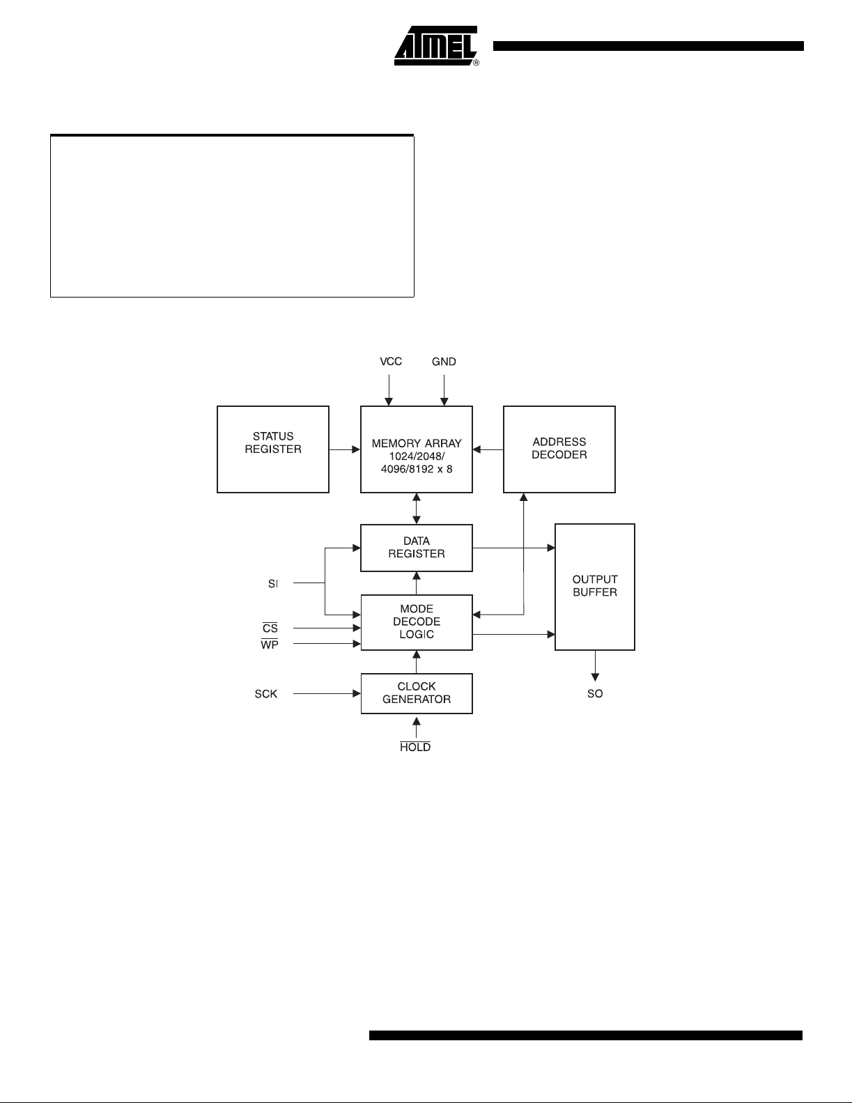
Block Diagram
*NOTICE: Stresses beyond those listed under “Absolute
Maximum Ratings” may cause permanent damage to the device . This is a stress r ating onl y and
functional operation of th e device at these or any
other conditions beyond those indi cated in the
operational sections of this specification is not
implied. Exposure to absolute maximum rating
conditions f or e xtended p eriods may af fe ct devi ce
reliability.
2
AT25080/160/320/640
3260D–SEEPR–9/03
Page 3
AT25080/160/320/640
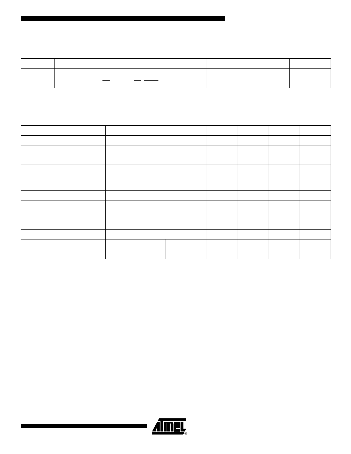
Pin Capacitance
(1)
Applicable over recommended operating range from TA = 25°C, f = 1.0 MHz, VCC = +5.0V (unless otherwise noted).
Symbol Tes t Condi ti ons Max Units Conditions
C
OUT
C
IN
Output Capacitanc e (SO) 8 pF V
Input Capacitance (CS, SCK, SI, WP, HOLD)6pFV
OUT
IN
= 0V
= 0V
Note: 1. This parameter is characterized and is not 100% tested.
DC Characteristics
(1)
Applicable over recommended operating range from: TA = -40°C to +125 °C, VCC = +2.7V to +5.5V
Symbol Parameter Test Condition Min Typ Max Units
V
CC1
V
Supply Voltage 4.5 5.5 V
CC2
I
Supply Current VCC = 5.0V at 1 MHz, SO = Open, Read 3.0 mA
CC1
I
Supply Current VCC = 5.0V at 2 MHz, SO = Open,
CC2
Standby Current VCC = 2.7V, CS = V
I
SB1
I
SB2
I
Input Leakage VIN = 0V to V
IL
I
OL
(1)
V
IL
(1)
V
IH
V
Output Low-voltage 2.7V ≤ VCC ≤ 5.5V IOL = 3.0 mA 0.4 V
OL1
V
OH1
Note: 1. VIL min and VIH max are reference onl y and are not tested.
Supply Voltage 2.7 5.5 V
5.0 mA
Read, Write
0.2 2.0 µA
2.0 5.0 µA
Standby Current VCC = 5.0V, CS = V
CC
Output Leakage V
= 0V to VCC -3.0 3.0 µA
IN
CC
CC
-3.0 µA
Input Low-voltage -0.6 VCC x 0.3 V
Input High-v oltage VCC x 0.7 VCC + 0.5 V
Output High-voltage IOH = -1.6 mA VCC - 0.8 V
3260D–SEEPR–9/03
3
Page 4
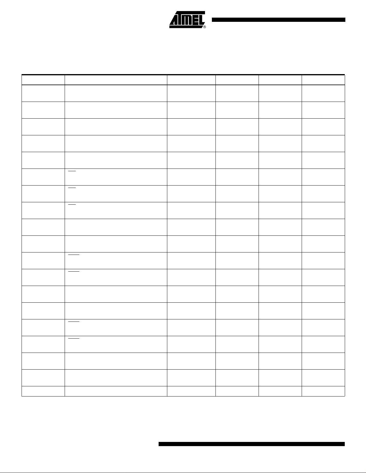
AC Characteristics
Applicable over recommended operating range from TA = -40°C to +125°C, VCC = As Specified,
CL = 1 TTL Gate and 100 pF (unless otherwise noted).
Symbol Parameter Voltage Min Max Units
f
SCK
SCK Clock Frequency 4.5 - 5.5
2.7 - 5.5
t
RI
Input Rise Time 4.5 - 5.5
2.7 - 5.5
t
FI
Input Fall Time 4.5 - 5.5
2.7 - 5.5
t
WH
SCK High Time 4.5 - 5.5
2.7 - 5.5
t
WL
SCK Low Time 4.5 - 5.5
2.7 - 5.5
t
CS
CS High Time 4.5 - 5.5
2.7 - 5.5
t
CSS
CS Setup Time 4.5 - 5.5
2.7 - 5.5
t
CS Hold Time 4.5 - 5.5
CSH
2.7 - 5.5
t
Data In Setup Time 4.5 - 5.5
SU
2.7 - 5.5
t
H
Data In Hold Time 4.5 - 5.5
2.7 - 5.5
t
Hold Setup Time 4.5 - 5.5
HD
2.7 - 5.5
0
0
133
200
133
200
250
250
250
250
250
250
50
50
50
50
100
100
3.0
2.1
2
2
2
2
ns
MHz
µs
µs
ns
ns
ns
ns
ns
ns
t
CD
t
V
t
HO
t
LZ
t
HZ
t
DIS
t
WC
Endurance
Hold Hold Time 4.5 - 5.5
Output Valid 4.5 - 5.5
Output Hold Time 4.5 - 5.5
Hold to Outp u t Low Z 4.5 - 5.5
Hold to Output High Z 4.5 - 5.5
Output Disabl e Time 4.5 - 5.5
Write Cycle Time 4.5 - 5.5
(1)
5.0V, 25°C, Page Mode 1M Write Cycles
Note: 1. This parameter is characterized and is not 100% tested.
4
AT25080/160/320/640
2.7 - 5.5
2.7 - 5.5
2.7 - 5.5
2.7 - 5.5
2.7 - 5.5
2.7 - 5.5
2.7 - 5.5
200
200
0
0
0
0
0
0
133
200
100
100
100
100
250
250
5
10
ns
ns
ns
ns
ns
ns
ms
3260D–SEEPR–9/03
Page 5

AT25080/160/320/640
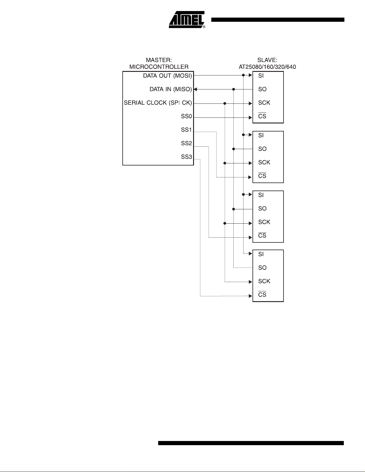
Serial Interface Description
MASTER: The device that generates the serial clock.
SLAVE: Because the Serial Clock pin (SCK) is always an input, the AT25080/160/320/640
always operates as a slave.
TRANSMITTER/RECEIVER: The AT25080/160/320/640 has separate pins designated for
data transmission (SO) and reception (SI).
MSB: The Most Significant Bit (MSB) is the first bit transmitted and received.
SERIAL OP-CODE: After the device is selected with CS
received. This byte contains the op-code that defines the operations to be performed.
INVALID O P-COD E: If an invalid op-code is received, no data will be shifted into the
AT25080/160/320/640, and the serial output pin (SO) will remain in a high impedance state
until the falling edge of CS
CHIP SELECT: The AT25080/160/320/640 is selected when the CS
device is not selected, data will not be accept ed via the SI pin, and the serial output pin (SO)
will remain in a high impedance state.
HOLD: The HOLD
AT25080/160 /320/640. When the dev ice is selected and a serial sequ ence is underway ,
HOLD
can be used to pause the serial communication with the master device without resetting
the serial sequence. To pause, the HOLD
To resume serial communication, the HOLD
may still toggle during HOLD
high impedance state.
is detected again. This will reinitialize the serial communication.
pin is used in conjunction with the CS pin to select the
pin must be bro ugh t low whil e the S CK pin is l ow.
pin is brought high while the SCK pin is low (SCK
). Inputs to the SI pin will be ignored while the SO pin is in the
going low, the first byte will be
pin is low. When the
WRITE PROTECT: The write protect pin (WP
held high. When the WP pin is brought low and WPEN bit is “1”, all write operations to the status register are in hibited. WP
register. If the internal write cycle has al ready been initiated, WP
on any write operation to t he st atus register. Th e WP
bit in the status register is "0". This will allow t he user to install the AT25080/160/320/640 in a
system with the WP
pin functions are enabled when the WPEN bit is set to “1”.
pin tied to g round an d still b e able to write to the st atus register. All WP
going low while C S is still low will in terrupt a write to the st atus
) will allow normal read/write operations when
going low will have no effe ct
pin function is blocked when the WPEN
3260D–SEEPR–9/03
5
Page 6
SPI Serial Interface
6
AT25080/160/320/640
3260D–SEEPR–9/03
Page 7

AT25080/160/320/640
Functional Description
The AT25080/160/320/640 is designed to interface directly with the synchronous serial peripheral interface (SPI) of the 6805 and 68HC11 series of microcontrollers.
The AT25080/160/320/640 utilizes an 8-bit instruction register. The list of instructions and their
operation codes are contained in Table 1. All instructions, addresses, and data are transferred
with the MSB first and start with a high-to-low CS transition.
Table 1. Instruction Set for the AT25080/160/320/640
Instruction Name Instruction Format Operation
WREN 0000 X110 Set Write Enable Latch
WRDI 0000 X100 Reset Write Enable Latch
RDSR 0000 X101 Read Status Register
WRSR 0000 X001 Write Status Register
READ 0000 X011 Read Data from Memory Array
WRITE 0000 X010 Write Data to Memory Array
WRITE ENA BLE ( WRE N): The device will power-up in the w rite disable state when V
CC
is
applied. All programming instruc tions must therefore be preceded by a Write Enabl e
instruction.
WRITE DISABLE (WRDI): To protect the device ag ainst inadvertent writes, the Write Disabl e
instruction disabl es all prog ramm ing modes . The WRD I instructi on is inde penden t of the status of the WP
pin.
READ STATUS REGISTER (RDSR): The Read Status Register instruction provides access to
the status register. The READY/BUSY and Write Enable status of the device can be determined by the RDSR instruction. Similarly, the Block Write Protection bits indicate the extent of
protection employed. These bits are set by using the WRSR instruction.
Table 2. Status Register Format
Bit 7 Bit 6 Bit 5 Bit 4 Bit 3 Bit 2 Bit 1 Bit 0
WPEN X X X BP1 BP0 WEN RDY
Table 3. Read Status Register Bit Definition
Bit Definition
Bit 0 (RDY
Bit 1 (WEN) Bit 1= 0 indicates the device is not WRITE ENABLED. Bit 1 = 1 indicates the
Bit 2 (BP0) See Table 4 on page 8.
Bit 3 (BP1) See Table 4 on page 8.
Bits 4 - 6 are 0s when device is not in an internal write cycle.
Bit 7 (WPEN) See Table 5 on page 8.
Bits 0 - 7 are 1s during an internal write cycle.
) Bit 0 = 0 (RDY) in dicates the device is READY. Bit 0 = 1 indi cates the write cycle is
in progress.
device is WRITE ENABLED.
3260D–SEEPR–9/03
7
Page 8

WRITE STATUS REGISTER (WRSR): The WRSR instruction allows the user t o sel ec t one of
four levels of pr otectio n. The A T25080 /160/32 0/640 is divide d into four arra y segm ents. On e
quarter (1/4), one half (1/2), or all of the m em ory s eg men ts ca n b e protected. Any of t he dat a
within any selected segment will therefore be READ only. The block write protection levels and
corresponding status register control bits are shown in Table 4.
The three bits, BP0, BP1, and WPEN are nonvolatile cells that have the same properties and
functions as the regular memory cells (e.g. WREN, t
, RDSR).
WC
Table 4. Block Write Protect Bits
Status
Register Bits Array Addresses Protected
Level
0 0 0 None None None None
1(1/4)
2(1/2)
3(All)
The WRSR instruction also allows the user to enable or disable the write protect (WP
BP1 BP0 AT25080 AT25160 AT25320 AT25640
01
10
11
0300
-03FF
0200
-03FF
0000
-03FF
0600
-07FF
0400
-07FF
0000
-07FF
0C00
-0FFF
0800
-0FFF
0000
-0FFF
1800
-1FFF
1000
-1FFF
0000
-1FFF
) pin
through the use of the W rite Protect En able (W PEN) bi t. Hardware w rite protection is enabled
when the WP
either the WP
pin is low and the WPE N bit is “1”. Hardware write protect ion is disabl ed when
pin is high or the WPEN bit is “0”. When the device is hardware write protected,
writes to the Status Register, including the Block Protect bits and the WPEN bit, and the blockprotected sections in the memory array are disabled. Writes are only allowed to sections of the
memory which are not block-protected.
NOTE: When the WPEN bit is hardware write protected, it cannot be changed back to “0”, as
long as the WP
pin is held low.
Table 5. WPEN Operation
WPEN WP WEN
Protected
Blocks
Unprotected
Blocks
Status
Register
0 X 0 Protected Protected Protected
0 X 1 Protected Writable Writable
1 Low 0 Protected Protected Protected
1 Low 1 Protected Writable Protected
X High 0 Protected Protected Protected
X High 1 Protected Writable Writable
8
AT25080/160/320/640
3260D–SEEPR–9/03
Page 9

AT25080/160/320/640
READ SEQUENCE (READ): Readin g the AT 2508 0 /16 0/320 /64 0 v ia th e SO (S eria l Ou tpu t)
pin requires the following sequence. After the CS
READ op-code is transmitted via the SI line followed by the byte address to be read (A15 - A0,
Refer to Table 6). Upon completion, any data on the SI line will be ignored. The data (D7 - D0)
at the specified address is then shi fted out ont o t he SO l ine. If onl y o ne byt e is to be read, t he
CS
line should b e driven h igh af ter the data co mes out. The REA D s equence can b e continued since the b yte ad dres s is aut om aticall y incr eme nted an d d ata w ill cont inue to be shifte d
out. When the highest address is reached, the address counter will roll over to the lowest
address allowing the entire memory to be read in one continuous READ cycle.
WRITE SEQUENCE (WRITE): In orde r to p rog ram th e AT 2508 0/1 60/320 /64 0, two sep arat e
instructions must be e xecuted. First, the device must be write enabled via the Write Enable
(WREN) Instruction. Then a Write (W RITE) Instruction m ay be ex ecut ed. A lso, th e address of
the memory location(s) to be programmed must be outside the protected address field location
selected by the Block Write Protection Level. During an internal write cycle, all commands will
be ignored except the RDSR instruction.
line is pulled low to select a device, the
A Write Instruction requires the following sequence. After the CS
line is pulled low to select the
device, the WRIT E op-cod e is transmitt ed via the S I line follo wed by th e byte add ress (A15 A0) and the data (D7 - D0) t o be program m ed (Refer to Table 6 ). Programm ing will start after
the CS
pin is brought high. The Low-to-High transition of the CS pin must occur during the
SCK low-time immediately after clocking in the D0 (LSB) data bit.
The READY/BUSY status of the device can be determined by initiating a READ STATUS
REGISTER (RDSR) Ins tru ction. If Bit 0 = 1, the WRITE cycle is stil l in progress. If Bit 0 = 0, the
WRITE cycle has en ded. Only the READ ST ATUS RE GISTER instru ction is en abled during
the WRITE programming cycle.
The AT25080/160/320/640 is capable of a 32-byte PAGE WRITE operation. After each byte of
data is received, the five low order address bits are internally incremented by one; the high
order bits o f the a ddres s wil l remai n c onsta nt. If more t han 32 byte s of da ta a re tra nsmi tted,
the address counter will roll ov er and the previously written d ata will be overwritten. The
AT25080/160/320/640 is automa tically returned to the write disable state at the completion of
a WRITE cycle.
NOTE: If the device is not Write enabled (WRE N), the devi ce will ignore th e Write instruction
and will return to the standby state, when CS
is brought high. A new CS falling edge is
required to re-initiate the serial communication.
Table 6. Address Key
Address AT25080 AT25160 AT25320 AT25640
A
N
Don't
Care Bits
A9 - A
A
15
- A
0
10
A10 - A
A15 - A
0
11
A11 - A
A
- A
15
0
12
A12 - A
A15 - A
0
13
3260D–SEEPR–9/03
9
Page 10

Timing Diagrams
Synchronous Data Timing (for Mode 0)
V
IH
CS
V
IL
t
CSS
V
SO
IH
V
IL
t
SU
V
IH
SI
V
IL
V
OH
HI-Z
V
OL
VALID IN
SCK
WREN Timing
t
CS
t
CSH
t
WH
t
H
t
WL
t
V
t
HO
t
DIS
HI-Z
WRDI Timing
10
AT25080/160/320/640
3260D–SEEPR–9/03
Page 11

RDSR Timing
AT25080/160/320/640
CS
WRSR Timing
SCK
CS
SCK
SI
SI
SO
01234567891011121314
INSTRUCTION
HIGH IMPEDANCE
00112233445566778 9 10 11 12 13 14 15
INSTRUCTION
76543210
MSB
DATA OUT
DATA IN
15
3260D–SEEPR–9/03
SO
HIGH IMPEDANCE
11
Page 12

READ Timing
CS
WRITE Timing
CS
SCK
SI
SCK
SI
SO
0
1
2
3
INSTRUCTION
HIGH IMPEDANCE
0
1
2
3
445566778910
INSTRUCTION
445566778910
BYTE ADDRESS
15 14 13
BYTE ADDRESS DATA IN
15 14 13
11 20 21 22 23 24 25 26 27 28 29 30
...
3
0
1
2
31
DATA OUT
0
1
2
3
MSB
11 20 21 22 23 24 25 26 27 28 29 30 31
...
3
0
1
2
1
2
3
0
HOLD
12
HIGH IMPEDANCE
SO
Timin g
CS
SCK
t
HD
HOLD
SO
AT25080/160/320/640
t
CD
t
HD
t
HZ
t
CD
t
LZ
3260D–SEEPR–9/03
Page 13
AT25080/160/320/640
AT250 80 Orderin g Informatio n
Ordering Code Package Operation Range
AT25080-10PA-5.0C
AT25080N-10SA-5.0C
AT25080-10PA-2.7C
AT25080N-10SA-2.7C
8P3
8S1
8P3
8S1
Automotive
(-40°C to 125°C)
Automotive
(-40°C to 125°C)
Package Type
8P3 8-lead, 0.300" Wide, Plastic Dual Inline Package (PDIP)
8S1 8-lead, 0.150" Wide, Plastic G ull Wing Small Outline (JEDEC SOIC)
Options
-5.0 Standard Device (4.5V to 5.5V)
-2.7 Low Voltage (2.7V to 5.5V)
3260D–SEEPR–9/03
13
Page 14

AT251 60 Orderin g Informatio n
Order i n g Code Pa ckag e Opera t i on Range
AT25160-10PA-5.0C
AT25160N-10SA-5.0C
AT25160-10PA-2.7C
AT25160N-10SA-2.7C
8P3
8S1
8P3
8S1
Automotive
(-40°C to 125 °C)
Automotive
(-40°C to 125 °C)
Package Type
8P3 8-lead, 0.300" Wide, Plastic Dual Inline Package (PDIP)
8S1 8-lead, 0.150" Wide, Plastic G ull Wing Small Outline (JEDEC SOIC)
Options
-5.0 Standard Device (4.5V to 5.5V)
-2.7 Low Voltage (2.7V to 5.5V)
14
AT25080/160/320/640
3260D–SEEPR–9/03
Page 15

AT25080/160/320/640
AT253 20 Orderin g Informatio n
Order i n g Code Pa ckag e Opera t i on Range
AT25320-10PA-5.0C
AT25320N-10SA-5.0C
AT25320-10PA-2.7C
AT25320N-10SA-2.7C
8P3
8S1
8P3
8S1
Automotive
(-40°C to 125 °C)
Automotive
(-40°C to 125 °C)
Package Type
8P3 8-lead, 0.300" Wide, Plastic Dual Inline Package (PDIP)
8S1 8-lead, 0.150" Wide, Plastic G ull Wing Small Outline (JEDEC SOIC)
Options
-5.0 Standard Device (4.5V to 5.5V)
-2.7 Low Voltage (2.7V to 5.5V)
3260D–SEEPR–9/03
15
Page 16
AT256 40 Orderin g Informatio n
Order i n g Code Pa ckag e Opera t i on Range
AT25640-10PA-5.0C
AT25640N-10SA-5.0C
AT25640-10PA-2.7C
AT25640N-10SA-2.7C
8P3
8S1
8P3
8S1
Automotive
(-40°C to 125 °C)
Automotive
(-40°C to 125 °C)
Package Type
8P3 8-lead, 0.300" Wide, Plastic Dual Inline Package (PDIP)
8S1 8-lead, 0.150" Wide, Plastic G ull Wing Small Outline (JEDEC SOIC)
Options
-5.0 Standard Device (4.5V to 5.5V)
-2.7 Low Voltage (2.7V to 5.5V)
16
AT25080/160/320/640
3260D–SEEPR–9/03
Page 17

Packaging Information
8P3 – PDIP
AT25080/160/320/640
D1
b3
4 PLCS
Top View
D
e
Side View
N
1
b
b2
A2 A
E
E1
c
eA
End View
COMMON DIMENSIONS
(Unit of Measure = inches)
SYMBOL
A 0.210 2
A2 0.115 0.130 0.195
b 0.014 0.018 0.022 5
b2 0.045 0.060 0.070 6
b3 0.030 0.039 0.045 6
c 0.008 0.010 0.014
D 0.355 0.365 0.400 3
L
D1 0.005 3
E 0.300 0.310 0.325 4
E1 0.240 0.250 0.280 3
e 0.100 BSC
eA 0.300 BSC 4
L 0.115 0.130 0.150 2
MIN
NOM
MAX
NOTE
Notes: 1. This drawing is for general information only; refer to JEDEC Drawing MS-001, Variation BA for additional information.
3260D–SEEPR–9/03
2. Dimensions A and L are measured with the package seated in JEDEC seating plane Gauge GS-3.
3. D, D1 and E1 dimensions do not include mold Flash or protrusions. Mold Flash or protrusions shall not exceed 0.010 inch.
4. E and eA measured with the leads constrained to be perpendicular to datum.
5. Pointed or rounded lead tips are preferred to ease insertion.
6. b2 and b3 maximum dimensions do not include Dambar protrusions. Dambar protrusions shall not exceed 0.010 (0.25 mm).
TITLE
2325 Orchard Parkway
R
San Jose, CA 95131
8P3, 8-lead, 0.300" Wide Body, Plastic Dual
In-line Package (PDIP)
DRAWING NO.
8P3
01/09/02
REV.
B
17
Page 18

8S1 – JEDEC SOIC
Top View
1
2
3
H
N
A2
L
e
D
Side View
E
End View
B
A
COMMON DIMENSIONS
(Unit of Measure = mm)
SYMBOL
A – – 1.75
B – – 0.51
C
C – – 0.25
D – – 5.00
E – – 4.00
e 1.27 BSC
H – – 6.20
L – – 1.27
MIN
NOM
MAX
NOTE
18
Note:
This drawing is for general information only. Refer to JEDEC Drawing MS-012 for proper dimensions, tolerances, datums, etc.
TITLE
2325 Orchard Parkway
R
San Jose, CA 95131
8S1, 8-lead (0.150" Wide Body), Plastic Gull Wing
Small Outline (JEDEC SOIC)
AT25080/160/320/640
DRAWING NO.
8S1 A
3260D–SEEPR–9/03
10/10/01
REV.
Page 19

Atmel Corporation Atmel Operations
2325 Orchard Park way
San Jose, CA 95131, USA
Tel: 1(408) 4 41-0311
Fax: 1(408) 487-260 0
Regional Headquarters
Europe
Atmel Sa rl
Route des Ars enau x 41
Case Postale 8 0
CH-1705 Fri bourg
Switzerland
Tel: (41) 26-4 26-55 55
Fax: (41) 26 -426-550 0
Asia
Room 121 9
Chinachem Gold en Plaza
77 Mody Ro ad Tsims hatsu i
East Kowloon
Hong Kong
Tel: (852) 27 21-9778
Fax: (852) 2 722-136 9
Japan
9F, Tonetsu Sh inkaw a Bl dg.
1-24-8 Shi nkawa
Chuo-ku, Tok yo 10 4-0033
Japan
Tel: (81) 3-35 23-35 51
Fax: (81) 3-3 523-758 1
Memory
2325 Orch ard Parkw ay
San Jose, C A 95131 , USA
Tel: 1(408 ) 441-031 1
Fax: 1(408) 43 6-43 14
Microcontrollers
2325 Orch ard Parkw ay
San Jose, C A 95131 , USA
Tel: 1(408 ) 441-031 1
Fax: 1(408) 43 6-43 14
La Chantrer ie
BP 70602
44306 Na ntes Cede x 3, Fra nce
Tel: (33) 2-4 0-18 -18-18
Fax: (33) 2-40-18-19-60
ASIC/ASSP/Smart Cards
Zone In dustrielle
13106 Rousse t Ced ex, France
Tel: (33) 4-4 2-53 -60-00
Fax: (33) 4-42-53-60-01
1150 East C heyenn e Mtn. Blvd.
Colorado Sp rings, CO 8 0906, USA
Tel: 1(719 ) 576-330 0
Fax: 1(719) 54 0-17 59
Scottish Enterprise Technology Park
Maxwell Building
East Kilbrid e G7 5 0QR, S cotlan d
Tel: (44) 13 55-803- 000
Fax: (44) 1355 -242 -743
RF/Automotive
Theresienstrasse 2
Postfach 3535
74025 Heilbr onn, Ge rmany
Tel: (49) 71-31-67-0
Fax: (49) 71 -31-67- 2340
1150 East Ch eyenne M tn. B lvd.
Colorado Spr ings, CO 80 906, USA
Tel: 1(719) 57 6-3300
Fax: 1(719) 540-1759
Biometrics/Imaging/Hi-Rel MPU/
High Speed Converters/RF Datacom
Avenue de R ocheplei ne
BP 123
38521 Saint- Egreve Cedex, France
Tel: (33) 4-76-58-30-00
Fax: (33) 4-7 6-58-3 4-80
Literature Requests
www.atmel.com/literature
Disclaimer: Atmel Corporation makes no warranty for the use of its products, other than those expressly contained in the Company’s standard
warranty which is detailed in Atmel’s Terms and Conditions located on the Company’s web site. The Company assumes no responsibility for any
errors which may appear in this document, reserves the right to change devices or specifications detailed herein at any time without notice, and
does no t make any com mitment to u pdate the informat ion contai ned herei n. No licen ses to paten ts or othe r intellect ual proper ty of Atmel are
granted by th e Com pany in conn ecti on w ith t he sale of A tme l pr oduc ts, exp ressl y or by im pli catio n. Atme l’s pro duct s ar e no t aut ho rized for us e
as critical components in life support devices or systems.
© Atm el Corporatio n 2003. All rights reserved. Atmel® and combinations thereof, are the regi stered trademarks of Atmel Corporation or its
subsid ia ries. O th er terms and pro du c t n am es m ay be th e t ra d em arks o f others.
Printe d on rec ycled pape r.
3260D–SEEPR–9/03 xM
 Loading...