

Page 1
Features
• Serial Peripheral Interf ace (SPI) Compatible
• Supports SPI Modes 0 (0,0) and 3 (1,1)
• Medium-v olt age and Standard-voltage Operation
– 5.0 (V
– 2.7 (V
• 3 MHz Clock Rate (5V)
• 64-byte Page Mode and Byte Write Operation
• Block Write Pr otection
– Protect 1/4, 1/2, or Entire Array
• Write Protect (WP) Pin and Write Disable Instructions for
both Hardware and Software Data Protection
• Self-timed Write Cycle (5 ms Typica l)
• High-reliability
– Endurance: 100,000 Write Cycles
– Data Retention: >200 Years
• 8-lead PDIP, 8- lead JEDEC SOIC and 8-lead EIAJ SOIC Packages
= 4.5V to 5.5V)
CC
= 2.7V to 5.5V)
CC
SPI Serial
Automotive
EEPROMs
128K (16,384 x 8)
Description
The AT25128A/256A provides 131,072/262,144 bits of serial electrically-erasable programmable read only memory (EEPROM) organized as 16,384/32,768 words of 8 bits
each. The device is optimized for use in many industrial and commerc ial applications
where low-power and low-vol tage operation are essential. The devices are available in
space saving 8-lead PDIP, 8-lead JEDEC SOIC and 8-lead EIAJ SOIC (AT25256A)
packages. In addition, the entire family is available in 5.0V (4.5V to 5.5V) and 2.7V
(2.7V to 5.5V) versions.
Pin Configurations
CS
SO
WP
GND
CS
SO
WP
GND
8-lead PDIP
1
8
2
7
3
6
4
5
8-lead SOIC
1
2
3
4
8
7
6
5
VCC
HOLD
SCK
SI
VCC
HOLD
SCK
SI
Pin Name Function
CS
SCK Serial Data Clock
SI Serial Data Input
SO Serial Data Output
GND Ground
VCC Power Supply
WP
HOLD
NC No Connect
DC Don't Connect
Chip Se lec t
Write Protect
Suspends Serial Input
256K (32,768 x 8)
AT25128A
AT25256A
Preliminary
Rev. 3404A–SEEPR–10/03
1
Page 2
The AT25128A/256A is enabled through the Ch ip Sele ct pin (CS) an d accessed via a 3-wire interface consisting of Seria l
Data Input (SI), Serial Data Output (SO), and Serial Clock (SCK). All programming cycles are completely self-timed, and no
separate ERASE cycle is required before WRITE.
BLOCK WRITE protection is enabled by programming the status register with top ¼ , top ½ or entire array of write protection. Separate program enable and program disable instructions are provided for additional data protection. Hardware data
protection is provided via the WP
pin to protect against inadvertent write attempts to the status register. The HOLD pin may
be used to suspend any serial communication without resetting the serial sequence.
Absolute Maximum Ratings*
Operating Temperature.................................. -55°C to +125°C
Storage Temperature............................ ......... -65°C to +150°C
Voltage on Any Pin
with Resp e c t to Gr o und . .. ... ....... .. ... ....... ... .. .......-1.0V to +7.0 V
Maximum Operating Voltage .......................................... 6.25V
DC Output Current........................................................ 5.0 mA
*NOTICE: Str esses beyond th ose listed under “Absolute Max i-
mum Ratings” ma y cause permanent damage to the
device. This is a stress rating only and functional
operation of the device at these or any other conditions beyond those indicated in the operational sections of this specification is not implied. Exposure to
absolute maximum rating conditions for extended
periods may affect device reliability.
Block Diagram
16384/32768 x 8
2
AT25128A/256A [Preliminary]
3404A–SEEPR–10/03
Page 3
AT25128A/256A [Preliminary]
Pin Capacitance
(1)
Applicable over recommended operating range from TA = 25°C, f = 1.0 MHz, VCC = +5.0V (unless otherwise noted).
Symbol T est Conditions Max Units Conditions
C
OUT
C
IN
Output Capacitance (SO) 8 pF V
Input Capacit ance (CS, SCK, SI, WP, HOLD)6pFV
OUT
IN
= 0V
= 0V
Note: 1. This parameter is characterized and is not 100% tested.
DC Characteristics
Applicable over recommended operating range from TA = -40°C to +125°C, VCC = +2.7V to +5.5V
Symbol Paramet er Test Condition Min Typ Max Units
V
CC1
V
CC2
I
CC1
I
CC2
I
SB1
I
SB2
I
IL
I
OL
(1)
V
IL
(1)
V
IH
V
OL1
V
OH1
Note: 1. V
Supply Voltage 2.7 5.5 V
Supply Voltage 4.5 5.5 V
Supply Current VCC = 5.0V at 1 MHz, SO = Open, Read 2.0 3.0 mA
= 5.0V at 2 MHz,
V
Supply Current
CC
SO = Open, Read, Write
Standby Current VCC = 2.7V, CS = V
Standby Current VCC = 5.0V, CS = V
Input Leakage VIN = 0V to V
CC
CC
CC
-3.0 3.0 µA
3.0 5.0 mA
0.2 2.0 µA
2.0 5.0 µA
Output Leakage VIN = 0V to VCC -3.0 3.0 µA
Input Low-voltage -1.0 VCC x 0.3 V
Input High-v oltage VCC x 0.7 VCC + 0.5 V
Outp u t Lo w -voltag e
Output High-voltage IOH = -1.6 mA VCC - 0.8 V
4.5 ≤ V
and VIH max are reference only and are not tested.
IL
≤ 5.5V
CC
I
= 3.0 mA 0.4 V
OL
3404A–SEEPR–10/03
3
Page 4
AC Characteristics
Applicable over recommended operating range from TA = -40°C to +125°C, VCC = As Specified,
CL = 1 TTL Gate and 100 pF (unless otherwise noted).
Symbol Parameter Voltage Min Max Units
f
SCK
t
RI
t
FI
t
WH
t
WL
t
CS
t
CSS
t
CSH
t
SU
t
H
t
HD
SCK Clock Frequency
Input Rise Time
Input Fall Time
SCK High Time
SCK Low Time
CS High Time
CS Setup Time
CS Hold Time
Data In Setup Time
Data In Hold Time
Hold Setup Time
4.5 - 5.5
2.7 - 5.5
4.5 - 5.5
2.7 - 5.5
4.5 - 5.5
2.7 - 5.5
4.5 - 5.5
2.7 - 5.5
4.5 - 5.5
2.7 - 5.5
4.5 - 5.5
2.7 - 5.5
4.5 - 5.5
2.7 - 5.5
4.5 - 5.5
2.7 - 5.5
4.5 - 5.5
2.7 - 5.5
4.5 - 5.5
2.7 - 5.5
4.5 - 5.5
2.7 - 5.5
0
0
150
200
150
200
250
250
100
250
150
250
30
50
50
50
100
100
3.0
2.1
2
2
2
2
MHz
µs
µs
ns
ns
ns
ns
ns
ns
ns
ns
t
CD
t
V
t
HO
t
LZ
t
HZ
t
DIS
t
WC
Endurance
Hold Hold Time
Output Valid
Output Hold Time
Hold to Output Low Z
Hold to Output High Z
Output Disable Time
Write Cycle Time
(1)
5.0V, 25°C, Page Mode 100K Write Cycles
4.5 - 5.5
2.7 - 5.5
4.5 - 5.5
2.7 - 5.5
4.5 - 5.5
2.7 - 5.5
4.5 - 5.5
2.7 - 5.5
4.5 - 5.5
2.7 - 5.5
4.5 - 5.5
2.7 - 5.5
4.5 - 5.5
2.7 - 5.5
200
300
0
0
0
0
0
0
Note: 1. This parameter is characterized and is not 100% tested. Contact Atmel for further information.
4
AT25128A/256A [Preliminary]
150
200
100
200
100
200
200
250
5
10
ns
ns
ns
ns
ns
ns
ms
3404A–SEEPR–10/03
Page 5

AT25128A/256A [Preliminary]
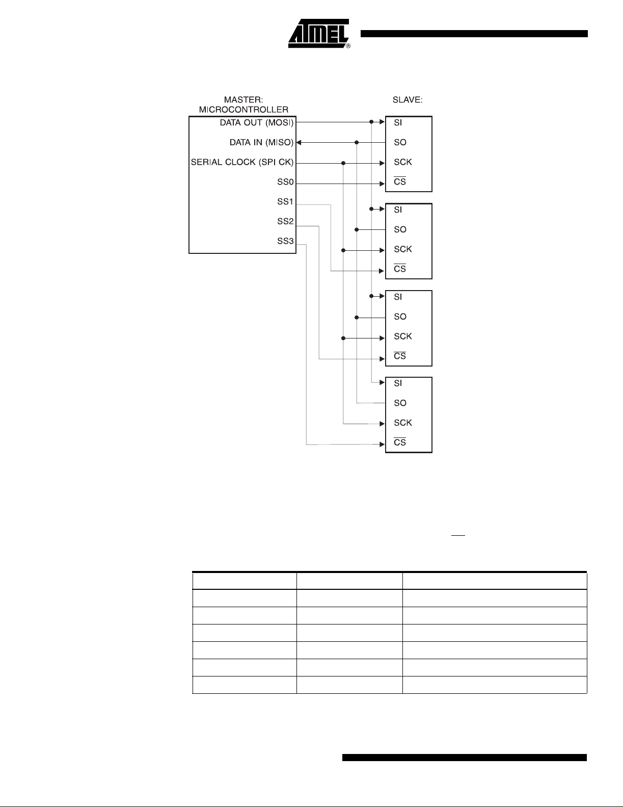
Serial Interface Description
MASTER: The device that generates the serial clock.
SLAVE: Be cause the Se rial Clock pi n (SCK) is alw ays an i nput, the AT2 5128A /256A
always operates as a slave.
TRANSMITTER/RECEIVER: The AT25128A/256A has separate pins designated for
data transmission (SO) and reception (SI).
MSB: The Most Significant Bit (MSB) is the first bit transmitted and received.
SERIAL OP-CODE: After th e device is selected with CS
be received. This byte contains the op-code that defines the operations to be performed.
INVALID OP-CODE: If an inv alid op-co de is rec eived, no data will be shifte d into the
AT251 28A /256 A, and th e ser ial out put pin ( SO) wi ll rem ain in a high im peda nce sta te
until the falling edge of CS
communication.
CHIP SELECT: The AT25128A/256A is selected when the CS
device is not selecte d, data wil l not be accepted via the S I pin, and the serial output pi n
(SO) will remain in a high impedance state.
HOLD: The HOLD
AT25128A/ 256A. Whe n the device is selected an d a serial seque nce is underway ,
HOLD
can be used to pause the serial communication with the master device without
resett ing th e s erial sequ en ce. To pa use, th e HOLD
SCK pin is low. To resume serial communication, the HOLD
SCK pin is low (SCK ma y still toggle duri ng HOLD
while the SO pin is in the high impedance state.
pin is used in conjunction with the CS pin to s elect th e
is detecte d again. This will rein itialize the seri al
pin mu st be brou gh t low whil e the
). Inputs to the SI pin will be i gnored
going low, the first byte will
pin is low. When the
pin is brought high while the
WRITE PROTECT: The write pro tect pin (WP
when he ld hi gh. Wh en the W P
tions to the status register are inhibited. WP
write to the status register. If the internal write cycle has already been initiated, WP
going lo w will ha ve n o effe ct on any wri te o perat ion to the status r egis ter . The WP pi n
funct ion is b loc ke d w hen th e WP EN bi t in the st atu s reg is ter is “ 0” . Thi s wi ll all ow th e
user to install the AT25128A/256A in a system with the WP
able to write to the status register. All WP
is set to “1”.
pin is brought low and WPEN bit is “1”, all write opera-
) will allo w no rmal read /wr ite o perat io ns
going low while CS is still low will interrupt a
pin tied to ground and still be
pin functions are enabled when the WPEN bit
3404A–SEEPR–10/03
5
Page 6
SPI Serial Interface
AT25128A/256A
Functional Description
6
AT25128A/256A [Preliminary]
The AT25128A/256A is designed to interface directly with the synchronous serial
peripheral interface (SPI) of the 6800 type series of microcontrollers.
The AT25128A/256A utilizes an 8-bit instruction register. The list of instructions and
their operation codes are contained in Table 1. All instructions, addresses, and data are
transferred with the MSB first and start with a high-to-low CS
Table 1. Instruction Set for the AT25128A/256A
Instruction Name Instruction Format Operation
WREN 0000 X110 Set Write Enable Latch
WRDI 0000 X100 Reset Write Enable Latch
RDSR 0000 X101 Read Status Register
WRSR 0000 X001 Write Status Registe r
READ 0000 X011 Read Data from Memory Array
WRITE 0000 X010 Write Data to Memory Array
transition..
3404A–SEEPR–10/03
Page 7

AT25128A/256A [Preliminary]
WRITE ENABLE (WREN): The device will power-up in the write disable state when V
CC
is applied. All prog ramm ing instruct ions must t herefore be pre cede d by a Write Enable
instruction.
WRITE DISA BLE (W RDI): To protect the device against inadvertent writes, the Write
Disable inst ruction d isable s all prog ramm ing mode s. Th e WRDI instructi on is ind ependent of the status of the WP
pin.
READ STATUS REGISTER (RDSR): The Read Status Register instruction provides
access to the status register. The READY/ BUSY and W rite Enable status of the device
can be determined by the RDSR instruction. Similarly, the Block Write Protection
bits indicate the extent of protection
instruction
.
employed. These bits are set by using the WRSR
Table 2. Status Register Format
Bit 7 Bit 6 Bit 5 Bit 4 Bit 3 Bit 2 Bit 1 Bit 0
WPEN X X X BP1 BP0 WEN RDY
Table 3. Read Status Register Bit Definition
Bit Definition
Bit 0 (RDY)Bit 0 = 0 (RDY) indicates the device is READY.
Bit 0 = 1 indicates the write cycle is i n progress.
Bit 1 (WEN) B it 1 = 0 indi cates t he de vi ce
the device is WRITE ENABLED.
is not
WRITE ENABLED . Bit 1 = 1 indicat es
Bit 2 (BP0) See Table 4.
Bit 3 (BP1) See Table 4.
Bits 4 - 6 are 0s when device is not in an internal write cycle.
Bit 7 (WPEN) See Table 5.
Bits 0 - 7 are 1s during an internal write cycle.
WRITE STATUS REGISTER (WRSR): The WRSR instruction allows the user to select
one of four levels of protection. The AT25128A/256A is divided into four array segments.
Top quarter (1/4), top half (1/2), or all of the memory segments can be protected. Any of
the data within any selected segment will therefore be REA D only. The block write protection levels and corresponding status register control bits are shown in Table 4.
The three bits, BP0, BP1, and WPEN are nonvolatile cells that have the same properties
and functions as the regular memory cells (e.g. WREN, t
, RDSR).
WC
Table 4. Block Write Protect Bits
Status Register Bits Array Addresses Protected
Level
0 0 0 None None
1(1/4) 0 1 3000 - 3FFF 6000 - 7FFF
2(1/2) 1 0 2000 - 3FFF 4000 - 7FFF
BP1 BP0 AT25128A AT25256A
3404A–SEEPR–10/03
3(All) 1 1 0000 - 3FFF 0000 - 7FFF
7
Page 8

The WRSR instruc tion als o allows t he user t o enab le or di sable the write prot ect (W P)
pin through the use of the Write Protect Enable (WPEN) bit. Hardware write protection is
enabled wh en the WP
disabled when
either
pin is low and t he WPE N bit is “1 ”. Hardware write protection is
the WP pin is high or the WPEN bit is “0.” When the device is hardware write protected, writes to the Status Regis ter, including the B lock Protec t bits and
the WPEN b it, and the bl ock-protec ted section s in the mem ory array are disa bled.
Writes are only allowed to sections of the memory which are not block-protected.
NOTE: When the WPEN bit is ha rdwa re write p rote cted, it cann ot be chan ged ba ck to
“0”, as long as the WP
pin is held low.
Table 5. WPEN Operation
Protected
WPEN WP WEN
0 X 0 Protected Protected Protected
0 X 1 Protected Writable Writable
1 Low 0 Protected Protected Protected
1 Low 1 Protected Writable Protected
X High 0 Protected Protected Protected
X High 1 Protected Writable Writable
Blocks
Unprotected
Blocks
Status
Register
READ SEQUENCE (READ): Reading the AT 25128A / 256A v ia the S O (S erial Output)
pin requires the following sequence. After the CS
line is pulled low to select a device,
the READ op-code is transm itted via the SI line followed by the by te addres s to be read
(Refer t o Tabl e 6). U po n co mpleti on , any data o n the S I line will b e ign ored. Th e dat a
(D7 - D0) at the specified address is then shifted out onto the SO line. If only one byte is
to be read, the CS
line should be dri ven high after the d ata comes out. The READ
sequence can be continued since the byte address is automatically incremented and
data will cont inue to be s hifted out . When t he hi ghest addres s is reach ed, the add ress
counter will roll over to the lowest address allowing the entire memory to be read in o ne
continuous READ cycle.
WRITE SEQUENCE (WRITE): In order to program the AT25128A/256A, two separate
instructions must be executed. First, the device must be write enabled via the Write
Enable (W REN) Instru ction . Then a W rite (WRIT E) Inst ruction m ay be exe cuted . Also,
the address of the memory location(s) to be programmed must be outside the protected
address field location selected by the Block Write Protection Level. During an internal
write cycle, all commands will be ignored except the RDSR instruction.
A Write Instruction requires the following sequence. After the CS
line is pulled low to
select the device, t he WRITE op-code is transmitted via the S I line f ollowed by the byte
address and the data (D7 - D0) to be program m ed (Refer to Table 6). Programm ing will
start after the CS
pin is brought high. (The LOW-to-High transition of the CS pin must
occur during the SCK low time immediately after clocking in the D0 (LSB) data bit.
The READY/BUSY status of the device can be determined by initiating a READ STA-
TUS REGISTER (RDSR) Instruction. If Bit 0 = 1, the WRITE cycle is still in progress. If
Bit 0 = 0, the WRITE cycle has ended. Only the READ STATUS REGISTER instruction
is enabled during the WRITE programming cycle.
8
AT25128A/256A [Preliminary]
3404A–SEEPR–10/03
Page 9

AT25128A/256A [Preliminary]
The AT25128A/256A is capable of a 64-byte PAGE WRITE operation. After each byte of
data is received, the six low order address bits are internally incremented by one; the
high order bits of the address will remain c onstant. If more than 64 by tes of data are
transmitted, the address counter will roll over and the pr eviously written data will be
overwritten. The AT25 128A /256A i s automat ically returned t o the w rite disabl e state at
the completion of a WRITE cycle.
NOTE: If the devi ce is not Write enabled (WREN), the devic e will ignore the Write
instruction and will return to th e st andby st at e, when CS
ing edge is required to re-initiate the serial communication.
Table 6. Address Key
Address AT25128A AT25256A
A
N
Don’t Care Bits A
A13 - A
15 - A14
is brought high. A new CS fall-
0
A14 - A
A
15
0
3404A–SEEPR–10/03
9
Page 10

Timing Diagrams (for S PI Mode 0 (0, 0))
Synchronous Data Timing
V
IH
CS
V
IL
t
CSS
V
WREN Timing
SCK
SO
IH
V
IL
t
SU
V
IH
SI
V
IL
V
OH
HI-Z
V
OL
VALID IN
t
WH
t
H
t
CS
t
CSH
t
WL
t
V
t
HO
t
DIS
HI-Z
WRDI Timing
10
AT25128A/256A [Preliminary]
3404A–SEEPR–10/03
Page 11

RDSR Timing
AT25128A/256A [Preliminary]
CS
WRSR Timing
SCK
SI
SO
01234567891011121314
INSTRUCTION
HIGH IMPEDANCE
76543210
MSB
DATA OUT
15
READ Timing
3404A–SEEPR–10/03
11
Page 12

WRITE Timing
HOLD Timing
SCK
HOLD
CS
SO
t
CD
t
HD
t
HD
t
HZ
t
CD
t
LZ
12
AT25128A/256A [Preliminary]
3404A–SEEPR–10/03
Page 13

AT25128A/256A [Preliminary]
AT25128A Ordering Information
Ordering Code Package Operation Range
AT25128A-10PA-5.0C
AT25128AN-10SA-5.0C
AT25128A-10PA-2.7C
AT25128AN-10SA-2.7C
8P3
8S1
8P3
8S1
Automotive
(-40°C to 125 °C)
Automotive
(-40°C to 125 °C)
Package Type
8P3 8-lead, 0.300" Wide, Plastic Dual In-line Package (PDIP)
8S1 8-lead, 0.150" Wide, Plastic Gull Wing Small Outline Package (JEDEC SOIC)
Options
-5.0 Standard Device (4.5V to 5.5V)
-2.7 Low-voltage (2.7V to 5.5V)
3404A–SEEPR–10/03
13
Page 14

AT25256A Ordering Information
Ordering Code Package Operation Range
AT25256A-10PA-5.0C
AT25256AN-10SA-5.0C
AT25256AW-10SA-5.0C
AT25256A-10PA-2.7C
AT25256AN-10SA-2.7C
AT25256AW-10SA-2.7C
8P3
8S1
8S2
8P3
8S1
8S2
Automotive
(-40°C to 125 °C)
Automotive
(-40°C to 125 °C)
Package Type
8P3 8-lead, 0.300" Wide, Plastic Dual In-line Package (PDIP)
8S1 8-lead, 0.150" Wide, Plastic Gull Wing Small Outline Package (JEDEC SOIC)
8S2 8-lead, 0.200" Wide, Plastic Gull Wing Small Outline Package (EIAJ SOIC)
Options
-5.0 Standard Device (4.5V to 5.5V)
-2.7 Low-voltage (2.7V to 5.5V)
14
AT25128A/256A [Preliminary]
3404A–SEEPR–10/03
Page 15

Packaging Information
8P3 – PDIP
AT25128A/256A [Preliminary]
D1
b3
4 PLCS
Top View
D
e
Side View
1
E
E1
N
c
eA
End View
COMMON DIMENSIONS
(Unit of Measure = inches)
b2
b
A2 A
SYMBOL
A 0.210 2
A2 0.115 0.130 0.195
b 0.014 0.018 0.022 5
b2 0.045 0.060 0.070 6
b3 0.030 0.039 0.045 6
c 0.008 0.010 0.014
D 0.355 0.365 0.400 3
L
D1 0.005 3
E 0.300 0.310 0.325 4
E1 0.240 0.250 0.280 3
e 0.100 BSC
eA 0.300 BSC 4
L 0.115 0.130 0.150 2
MIN
NOM
MAX
NOTE
Notes: 1. This drawing is for general information only; refer to JEDEC Drawing MS-001, Variation BA for additional information.
3404A–SEEPR–10/03
2. Dimensions A and L are measured with the package seated in JEDEC seating plane Gauge GS-3.
3. D, D1 and E1 dimensions do not include mold Flash or protrusions. Mold Flash or protrusions shall not exceed 0.010 inch.
4. E and eA measured with the leads constrained to be perpendicular to datum.
5. Pointed or rounded lead tips are preferred to ease insertion.
6. b2 and b3 maximum dimensions do not include Dambar protrusions. Dambar protrusions shall not exceed 0.010 (0.25 mm).
TITLE
2325 Orchard Parkway
R
San Jose, CA 95131
8P3, 8-lead, 0.300" Wide Body, Plastic Dual
In-line Package (PDIP)
DRAWING NO.
8P3
01/09/02
REV.
B
15
Page 16

8S1 – JEDEC SOIC
1
E
N
E1
L
Top View
A1
End View
e
D
Side View
b
A
SYMBOL
A 1.35 – 1.75
A1 0.10 – 0.25
b 0.31 – 0.51
C 0.17 – 0.25
D 4.80 – 5.00
E1 3.81 – 3.99
E 5.79 – 6.20
e 1.27 BSC
L 0.40 – 1.27
COMMON DIMENSIONS
(Unit of Measure = mm)
MIN
NOM
MAX
NOTE
16
Note:
These drawings are for general information only. Refer to JEDEC Drawing MS-012, Variation AA for proper dimensions, tolerances, datums, etc.
1150 E. Cheyenne Mtn. Blvd.
Colorado Springs, CO 80906
R
TITLE
8S1, 8-lead (0.150" Wide Body), Plastic Gull Wing
Small Outline (JEDEC SOIC)
DRAWING NO.
AT25128A/256A [Preliminary]
10/3/03
REV.
8S1 B
3404A–SEEPR–10/03
Page 17

8S2 – EIAJ SOIC
AT25128A/256A [Preliminary]
1
E
N
Top View
e
b
A
D
COMMON DIMENSIONS
(Unit of Measure = mm)
Side View
SYMBOL
A 1.70 2.16
A1
C
L
E1
End View
Notes: 1. This drawing is for general information only; refer to EIAJ Drawing EDR-7320 for additional information.
2. Mismatch of the upper and lower dies and resin burrs aren't included.
3. It is recommended that upper and lower cavities be equal. If they are different, the larger dimension shall be regarded.
4. Determines the true geometric position.
5. Values b,C apply to pb/Sn solder plated terminal. The standard thickness of the solder layer shall be 0.010 +0.010/-0.005 mm.
A1 0.05 0.25
b 0.35 0.48 5
C 0.15 0.35 5
D 5.13 5.35
E1 5.18 5.40 2, 3
E 7.70 8.26
L 0.51 0.85
e 1.27 BSC 4
MIN
NOM
MAX
NOTE
10/3/03
2325 Orchard Parkway
R
San Jose, CA 95131
3404A–SEEPR–10/03
TITLE
8S2, 8-lead, 0.209" Body, Plastic Small
Outline Package (EIAJ)
DRAWING NO.
8S2
REV.
C
17
Page 18

Atmel Corporation Atmel Operations
2325 Orchard Park way
San Jose, CA 95131, USA
Tel: 1(408) 4 41-0311
Fax: 1(408) 487-260 0
Regional Headquarters
Europe
Atmel Sa rl
Route des Ars enau x 41
Case Postale 8 0
CH-1705 Fri bourg
Switzerland
Tel: (41) 26-4 26-55 55
Fax: (41) 26 -426-550 0
Asia
Room 121 9
Chinachem Gold en Plaza
77 Mody Ro ad Tsims hatsu i
East Kowloon
Hong Kong
Tel: (852) 27 21-9778
Fax: (852) 2 722-136 9
Japan
9F, Tonetsu Sh inkaw a Bl dg.
1-24-8 Shi nkawa
Chuo-ku, Tok yo 10 4-0033
Japan
Tel: (81) 3-35 23-35 51
Fax: (81) 3-3 523-758 1
Memory
2325 Orch ard Parkw ay
San Jose, C A 95131 , USA
Tel: 1(408 ) 441-031 1
Fax: 1(408) 43 6-43 14
Microcontrollers
2325 Orch ard Parkw ay
San Jose, C A 95131 , USA
Tel: 1(408 ) 441-031 1
Fax: 1(408) 43 6-43 14
La Chantrer ie
BP 70602
44306 Na ntes Cede x 3, Fra nce
Tel: (33) 2-4 0-18 -18-18
Fax: (33) 2-40-18-19-60
ASIC/ASSP/Smart Cards
Zone In dustrielle
13106 Rousse t Ced ex, France
Tel: (33) 4-4 2-53 -60-00
Fax: (33) 4-42-53-60-01
1150 East C heyenn e Mtn. Blvd.
Colorado Sp rings, CO 8 0906, USA
Tel: 1(719 ) 576-330 0
Fax: 1(719) 54 0-17 59
Scottish Enterprise Technology Park
Maxwell Building
East Kilbrid e G7 5 0QR, S cotlan d
Tel: (44) 13 55-803- 000
Fax: (44) 1355 -242 -743
RF/Automotive
Theresienstrasse 2
Postfach 3535
74025 Heilbr onn, Ge rmany
Tel: (49) 71-31-67-0
Fax: (49) 71 -31-67- 2340
1150 East Ch eyenne M tn. B lvd.
Colorado Spr ings, CO 80 906, USA
Tel: 1(719) 57 6-3300
Fax: 1(719) 540-1759
Biometrics/Imaging/Hi-Rel MPU/
High Speed Converters/RF Datacom
Avenue de R ocheplei ne
BP 123
38521 Saint- Egreve Cedex, France
Tel: (33) 4-76-58-30-00
Fax: (33) 4-7 6-58-3 4-80
Literature Requests
www.atmel.com/literature
Disclaimer: Atmel Corporation makes no warranty for the use of its products, other than those expressly contained in the Company’s standard
warranty which is detailed in Atmel’s Terms and Conditions located on the Company’s web site. The Company assumes no responsibility for any
errors which may appear in this document, reserves the right to change devices or specifications detailed herein at any time without notice, and
does no t make any com mitment to u pdate the informat ion contai ned herei n. No licen ses to paten ts or othe r intellect ual proper ty of Atmel are
granted by th e Com pany in conn ecti on w ith t he sale of A tme l pr oduc ts, exp ressl y or by im pli catio n. Atme l’s pro duct s ar e no t aut ho rized for us e
as critical components in life support devices or systems.
© Atm el Corporati on 2003. All rights reserved. Atmel® and co mbinat ions th ereof, ar e the registe red trad emar ks of Atme l Cor porati on or its
subsid ia ries. O th er terms and pro du c t n am es m ay be th e t ra d em arks o f others.
Printe d on rec ycled pape r.
3404A–SEEPR–10/03 xM
 Loading...