

Page 1
Features
• Serial Peripheral Interf ace (SPI) Compatible
• Supports SPI Modes 0 (0,0) and 3 (1,1)
• Medium-v olt age and Standard-voltage Operation
– 5.0 (V
– 2.7 (V
• 3.0 MHz Clock Rate (5V)
• 8-byte Page M o de
• Block Write Pr otection
– Protect 1/4, 1/2, or Entire Array
• Write Protect (WP) Pin and Write Disable Instructions for
Both Hardware and Sof tware Data Protection
• Self-timed Write Cycle (10 ms max)
• High Reliability
– Enduranc e: One Million Write Cycles
– Data Retention: 100 Years
• 8-pin PDIP and 8-lead JEDEC SOIC Package
= 4.5V to 5.5V)
CC
= 2.7V to 5.5V)
CC
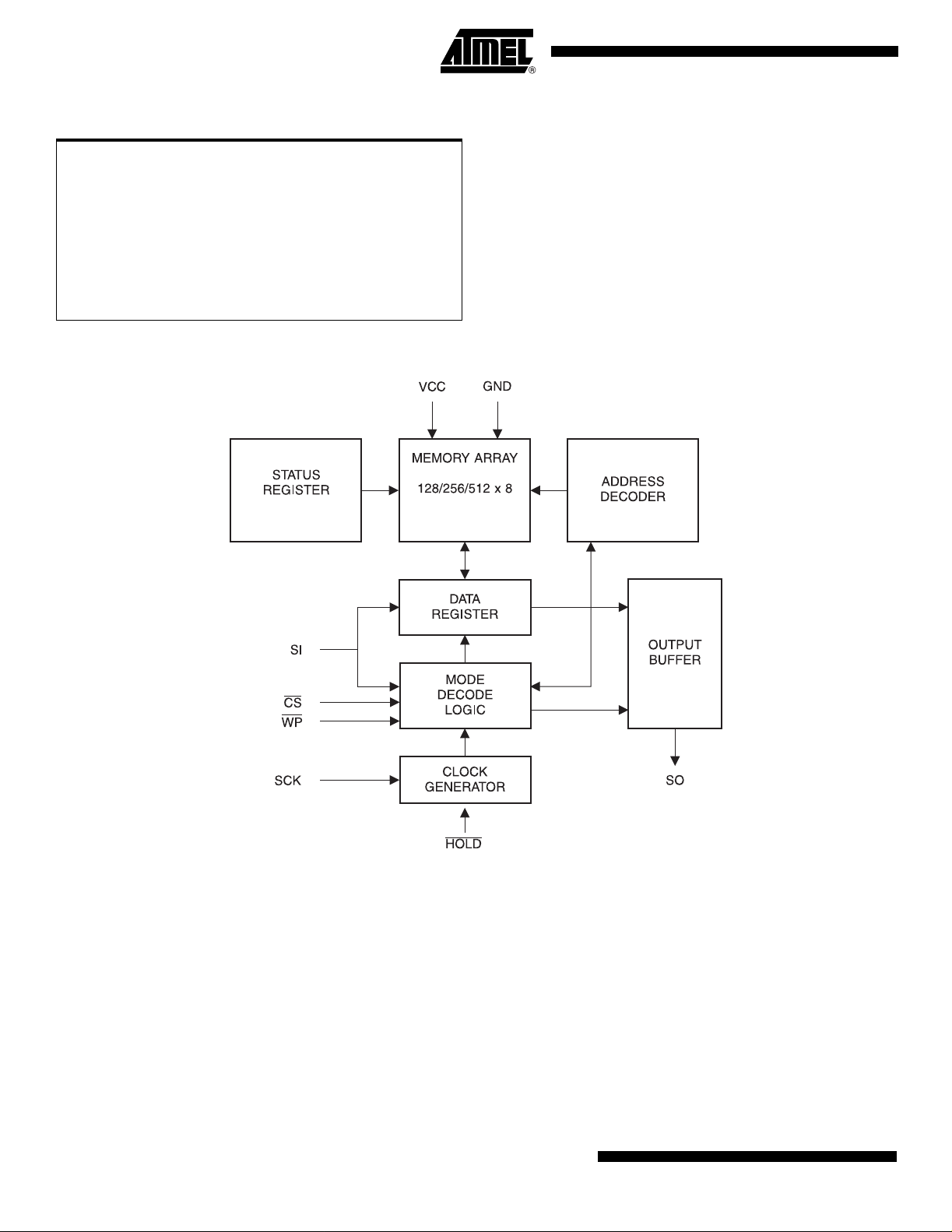
SPI Serial
Automotive
EEPROMs
1K (128 x 8)
Description
The AT25010A/020A/040A provides 1024/2048/4096 bits of serial electrically erasable programmable read only memory (EEPROM) organized as 128/256/512 words of
8 bits each. The device is optimized for use in many automotive applications where
low-power and low voltage operation are essential. The AT25010A/020A/040A is available in space saving 8-pin PDIP and 8-lead JEDEC SOIC packages.
The AT25010A/020A/040A is enabled through the Chip Select pin (CS
via a 3-wire interface consisting of Serial Data Input (SI), Serial Data Output (SO), and
Serial C lock (SC K). All programm ing cy cle s are c omp letely self-tim ed, and no sep arate ERASE cycle is required before WRITE.
BLOCK WRIT E protectio n is enabled by programmi ng the statu s registe r with on e of
four blocks of write protection. Separate program enable and program disable instructions are provided for additional data protection. Hardware data protection i s provided
via the WP
used to suspend any serial communication without resetting the serial sequence.
pin to protect against inadvertent write attempts. The HOLD pin may be
) and accessed
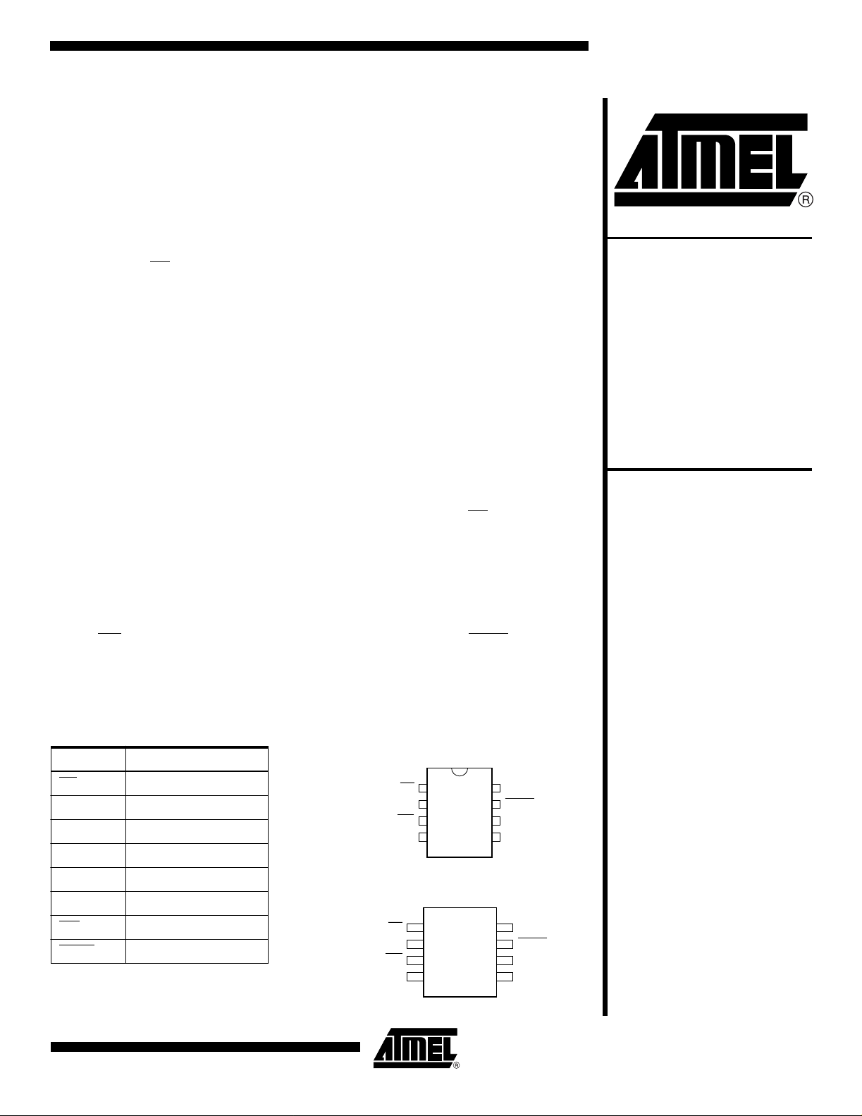
Pin Configurations
CS
SO
WP
8-pin PDIP
1
2
3
4
8
VCC
7
HOLD
6
SCK
5
SI
Pin Name Function
CS
SCK Serial Data Clock
SI Serial Data Input
SO Serial Data Output
Chip Select
GND
2K (256 x 8)
4K (512 x 8)
AT25010A
AT25020A
AT25040A
Preliminary
SPI, 1K Serial
2
E
PROM
GND Ground
VCC Power Supply
WP
HOLD
Write Protect
Suspends Serial Input
CS
SO
WP
GND
8-lead SOIC
1
2
3
4
8
7
6
5
VCC
HOLD
SCK
SI
Rev. 3402A–SEEPR–10/3/03
1
Page 2
Absolute Maximum Ratings*
Operatin g Temperature....... .. ........................ -55°C to + 1 25° C
Storage Temperature.................................... -65°C to + 150°C
Voltage on Any Pin
with Respect to Ground ....................................-1.0V to + 7.0V
Maximum Operating Voltage .......................................... 6.25V
DC Output Current........................................................ 5.0 mA
Block Diagram
*NOTICE: Stresses beyond those listed under “Absolute
Maximum Ratin gs” may cause permanent damage to the devi ce . This is a stres s rati ng only and
functional operation of the de vice at these or any
other conditions beyond those indicated in the
operational sections of this specif ication is not
implied. Expos ure to absolute maximum rat ing
conditions for ext ended periods may affect
device reliability.
2
AT25010A/020A/040A [Preliminary]
3402A–SEEPR–10/3/03
Page 3
AT25010A/020A/040A [Preliminary]
Pin Capacitance
(1)
Applicable over recommended operating range from TA = 25°C, f = 1.0 MHz, VCC = +5.0V (unless otherwise noted).
Symbol T est Conditions Max Units Conditions
C
OUT
C
IN
Output Capacitance (SO) 8 pF V
Input Capacit ance (CS, SCK, SI, WP, HOLD)6pFV
OUT
= 0V
IN
= 0V
Note: 1. This parameter is characterized and is not 100% tested.
DC Characteristics
Applicable over recommended operating range from: TA = -40°C to +125°C, VCC = +2.7V to +5.5V.
Symbol Parameter Te st Condi ti on Min Max Units
V
CC1
V
CC2
I
CC1
I
CC2
I
SB1
I
SB2
I
IL
I
OL
(2)
V
IL
(2)
V
IH
V
OL1
V
OH1
V
OL2
V
OH2
Notes: 1. This parameter is preliminary and Atmel may change the specifications upon further characterization.
Supply Voltage 2.7 5.5 V
Supply Voltage 4.5 5.5 V
Supply Current VCC = 5.0V at 1 MHz, SO = Open, Read 3.0 mA
= 5.0V at 2 MHz, SO = Open,
V
Supply Current
CC
Read, Write
Standby Current VCC = 2.7V CS = V
Standby Current VCC = 5.0V CS = V
CC
CC
6.0 mA
5µA
10 µA
Input Leakage VIN = 0V to VCC -0.6 3.0 µA
Output Leakage VIN = 0V to VCC -0.6 3.0 µA
Input Low Voltage -0.6 V
x 0.3 V
CC
Input High Voltage VCC x 0.7 VCC + 0.5 V
Outp u t Lo w Voltag e
Output High Voltage IOH = -1.0 mA VCC - 0.8 V
4.5V ≤ V
≤ 5.5V
CC
Outp u t Lo w Voltag e
Output High Voltage IOH = -100 µA VCC - 0.2 V
2.7V ≤ V
2. V
min and VIH max are reference onl y and are not tested.
IL
≤ 5.5V
CC
= 2.0 mA 0.4 V
I
OL
I
= 0.15 mA 0.2 V
OL
3402A–SEEPR–10/3/03
3
Page 4
AC Characteristics
Applicable over recommended operating range from TA = -40°C to +125°C, VCC = As Specified,
CL = 1 TTL Gate and 100 pF (unless otherwise noted).
Symbol Parameter Voltage Min Max Units
f
SCK
t
RI
t
FI
t
WH
t
WL
t
CS
t
CSS
t
CSH
t
SU
t
H
t
HD
t
CD
SCK Clock Frequency
Input Rise Time
Input Fall Time
SCK High Time
SCK Low Time
CS High Time
CS Setup Time
CS Hold0 Time
Data In Setup Time
Data In Hold Time
Hold Setup Time
Hold Hold Time
4.5 - 5.5
2.7 - 5.5
4.5 - 5.5
2.7 - 5.5
4.5 - 5.5
2.7 - 5.5
4.5 - 5.5
2.7 - 5.5
4.5 - 5.5
2.7 - 5.5
4.5 - 5.5
2.7 - 5.5
4.5 - 5.5
2.7 - 5.5
4.5 - 5.5
2.7 - 5.5
4.5 - 5.5
2.7 - 5.5
4.5 - 5.5
2.7 - 5.5
4.5 - 5.5
2.7 - 5.5
4.5 - 5.5
2.7 - 5.5
0
0
133
266
133
266
250
250
250
250
250
250
50
50
50
100
100
100
200
200
3.0
1.5
2
2
2
2
MHz
µs
µs
ns
ns
ns
ns
ns
ns
ns
ns
ns
t
V
t
HO
t
LZ
t
HZ
t
DIS
t
WC
Endurance
Output Valid
Output Hold Time
Hold to Output Low Z
Hold to Output High Z
Output Disable Time
Write Cycle Time
(1)
5.0V, 25°C, Page M o de 1M Wri t e Cycl es
Note: 1. This parameter is characterized and is not 100% tested.
4
AT25010A/020A/040A [Preliminary]
4.5 - 5.5
2.7 - 5.5
4.5 - 5.5
2.7 - 5.5
4.5 - 5.5
2.7 - 5.5
4.5 - 5.5
2.7 - 5.5
4.5 - 5.5
2.7 - 5.5
4.5 - 5.5
2.7 - 5.5
0
0
0
0
0
0
133
266
100
100
100
100
250
500
5
10
ns
ns
ns
ns
ns
ms
3402A–SEEPR–10/3/03
Page 5

AT25010A/020A/040A [Preliminary]
Serial Interface Description
MASTER: The device that generates the serial clock.
SLAVE: Because the Serial Clock pin (SCK) is always an input, the
AT25010A/020A/040A always operates as a slave.
TRANSMITTER/RECEIVER: The AT25010A/020A /040A has sepa rate pins des ignated
for data transmission (SO) and reception (SI).
MSB: The Most Significant Bit (MSB) is the first bit transmitted and received.
SERIAL OP-CODE: After the device is selected with CS
received. This byte contains the op-code that defines the operations to be performed.
The op-code also contains address bit A8 in both the READ and WRITE instructions.
INVALID OP-CODE: If an invalid op-code is received, no data will be shifted into the
AT250 10A /020A /040A , and the s erial out put p in (SO ) wil l remai n in a high imped an ce
state until the falling edge of CS
communication.
CHIP SELECT: The AT25010A/020A/040A is selected when the CS
the device is not selected, data will not be ac cept ed v ia the SI pin, and t he ser i al output
pin (SO) will remain in a high impedance state.
HOLD: The HOLD
AT25010A/020A/040A. When the device is selected and a serial sequence is underway,
HOLD
can be used to paus e the serial communication with the master device without
resett ing th e s erial sequ en ce. To pa use, th e HOLD
SCK pin is low. To resume serial communication, the HOLD
SCK pin is low (SCK ma y still toggle duri ng HOLD
while the SO pin is in the high impedance state.
pin is used in conjunction with the CS pin to s elect th e
is detected again. This will reinitialize the serial
going l o w , th e f ir s t byte will be
pin is lo w. W hen
pin mu st be brou gh t low whil e the
pin is brought high while the
). Inputs to the SI pin will be i gnored
WRITE PROTECT: The write pro tect pin (WP
when held high. When the WP
goin g lo w wh il e C S is still low will interrupt a write to the AT25010A/020A/040A. If
WP
the internal write cycle has already been initiated, WP
any write operation.
pin is brought low, all write operations are inhibited.
) will allo w no rmal read /wr ite o perat io ns
going low will have no effect on
3402A–SEEPR–10/3/03
5
Page 6
SPI Serial Interface
AT25010A/020A/040A
6
AT25010A/020A/040A [Preliminary]
3402A–SEEPR–10/3/03
Page 7

AT25010A/020A/040A [Preliminary]
Functional Description
The AT25010A/02 0A/040A is designed to interf ace directly with the synchro nous seria l
peripheral interface (SPI) of the 6805 and 68HC11 series of microcontrollers.
The A T25 010A / 020A /04 0A util izes an 8-bi t i nst ruct ion regi ste r. The li st of in stru ction s
and their operation codes are contained in Table 1. All instructions, addresses, and data
are transferred with the MSB first and start with a high-to-low CS
transition.
Table 1. Instruction Set for the AT25010A/020A/040A
Instructi on N ame Instructi on For m at Operation
WREN 0000 X110 Set Write Enable Latch
WRDI 0000 X100 Reset Write Enable Latch
RDSR 0000 X101 Read Status Register
WRSR 0000 X001 Write Status Register
READ 0000 A011 Read Data from Memory Array
WRITE 0000 A010 Write Data to Memory Array
Note: “A” repr esents MSB address bit A8.
WRITE ENAB LE (WR EN): The device will power up in the write disable state when
V
is applied. All programming instructions must therefore be preceded by a Write
CC
Enable instruction. The WP
pin must be held high during a WREN instruction.
WRITE DISABLE (WRDI): To protect the device again st inadvertent writes, the Write
Disable inst ruction d isable s all prog ramm ing mode s. Th e WRDI instructi on is ind ependent of the status of the WP
pin.
READ STATUS REGISTER (RDSR): The Re ad Sta tus R egist er in structi on provid es
access to the status register. The READY/ BUSY and W rite Enable status of the device
can be determined by the RDSR instruction. Similarly, the Block Write Protec tion bits
indicate the extent of protect ion empl oyed. Th ese bits a re set by us ing the WR SR
instruction.
Table 2. Status Register Format
Bit 7 Bit 6 Bit 5 Bit 4 Bit 3 Bit 2 Bit 1 Bit 0
X X X X BP1 BP0 WEN RDY
Table 3. Read Status Register Bit Definition
Bit Definition
Bit 0 (RDY
Bit 1 (WEN)
Bit 2 (BP0) See Table 4.
Bit 3 (BP1) See Table 4.
Bits 4-7 are 0s when device is not in an internal write cycle.
Bits 0-7 are 1s duri ng an internal write cyc le.
)
Bit 0 = 0 (RDY
write cycle is in progress.
Bit 1 = 0 indicates the device
the device is WR IT E ENA B LED.
) indicates the device is READY. Bit 0 = 1 indicates the
is not
WRITE ENABLED. Bit 1 = 1 indicates
3402A–SEEPR–10/3/03
7
Page 8

WRITE STATU S REGISTER (W RSR): The WRSR instruction allows the user to
select one of four levels of protection. The AT25010A/020A/040A is divided into four
array segments. Top quarter (1/4), Top half (1/2), or all of the memory segments can be
protected. Any of the data within any selected segment will therefore be READ only. The
block write protection levels and corresponding status register control bits are shown in
Table 4.
The two bits, BP1 and BP0 are nonvolatile cells that have the same properties and functions as the regular memory cells (e.g. WREN, t
, RDSR).
WC
Table 4. Block Write Protect Bits
Status Register Bits Array Addresses Protected
Level
000NoneNoneNone
1 (1/4) 0 1 60-7F C0-FF 180-1FF
2 (1/2) 1 0 40-7F 80-FF 100-1FF
3 (All) 1 1 00-7F 0 0-FF 0 00 - 1F F
BP1 BP0 AT25010A AT25020A AT25040A
READ SEQUENCE (READ): Reading the AT25010A/020A/040A via the SO (Serial
Output) p in req uires the f ollow in g sequ en ce. Aft er the C S
line is p ulle d l ow t o se le ct a
device , the READ op-c ode (incl udi ng A8) is tra ns mitte d via the SI line fol lowed by th e
byte addr ess to be read (A7- A0). Up on comp letion, an y data on the SI lin e will be
ignored. The data (D7-D0) at the specified address is then shifted out onto the SO line.
If only one byte is to be read, the CS
line should be driven high after the data comes out.
The READ sequence can be continued since the byte address is automatically incremented a nd data wi ll continu e to be shifted out. Whe n the highest ad dress i s reach ed,
the address counter will roll over to the lowest address allowing the entire memory to be
read in one continuous READ cycle.
WRITE SEQUENCE (WRITE): In order to program the AT 25010A/020A/040A, the
Write Protect pin (WP
) must be held high and two separate instructions must be executed. First, the device must be write enabled via the Write Enable (WREN)
Instruction. Then a Write (WRITE) Instruction may be executed. Also, the address of the
memory location(s) to be programmed must be outside the protected address field location selected by the Block Write Protection Level. During an internal write cycle, all
commands will be ignored except the RDSR instruction.
A Write Instruction requires the following sequence. After the CS
line is pulled low to
select the device, the WRITE op-code (including A8) is transmitted via the SI line followed by the byte address (A7-A0) and the data (D7-D0) to be programmed.
Programming will start after the CS
the CS
pin must occur during the SCK low time immediately after clocking in the D0
pin is brought high. (The LOW to High tra nsition of
(LSB) data bit.
The READY/BUSY status of the device can be determined by initiating a READ STA-
TUS REGISTER (RDSR) Instruction. If Bit 0 = 1, the WRITE cycle is still in progress. If
Bit 0 = 0, the WRITE cycle has ended. Only the READ STATUS REGISTER instruction
is enabled during the WRITE programming cycle.
8
AT25010A/020A/040A [Preliminary]
3402A–SEEPR–10/3/03
Page 9

AT25010A/020A/040A [Preliminary]
The AT25010A/020A/040 A is capable of an 8-byte PAGE WRITE operat ion. After each
byte of data i s received, the th ree low ord er address bits are i ntern ally incr emented by
one; the six high orde r bits of the ad dress w ill remai n constan t. If mo re than 8 by tes of
data are transmitted, the address counter will roll over and the previously written data
will be overwritten. The AT25010A/020A /040A is automatically returned to the write disable state at the completion of a WRITE cycle.
NOTE: If the W P
device will ignore th e Write i nstructi on and w ill retu rn to the stand by state, when C S
brought high. A new CS falling edge is required to re-initiate the serial communication.
pin is brought low or if the device is not Write enabled (WREN), the
is
3402A–SEEPR–10/3/03
9
Page 10

Timing Diagrams
Synchronous Data Timing (for mode 0)
V
IH
CS
V
IL
t
CSS
V
SO
IH
V
IL
t
SU
V
IH
SI
V
IL
V
OH
HI-Z
V
OL
VALID IN
SCK
WREN Timing
t
CS
t
CSH
t
WH
t
H
t
WL
t
V
t
HO
t
DIS
HI-Z
WRDI Timing
10
AT25010A/020A/040A [Preliminary]
3402A–SEEPR–10/3/03
Page 11

RDSR Timing
AT25010A/020A/040A [Preliminary]
CS
WRSR Timing
SCK
SCK
SI
SO
CS
SI
01234567891011121314
INSTRUCTION
HIGH IMPEDANCE
01234567891011121314
INSTRUCTION
76543210
MSB
76543210
DATA OUT
DATA IN
15
15
READ Timing
3402A–SEEPR–10/3/03
SO
HIGH IMPEDANCE
11
Page 12

WRITE Timing
CS
SCK
SI
SO
HOLD Timing
CS
SCK
HOLD
SO
01234567891011121314
INSTRUCTION
BYTE ADDRESS
801234567
9TH BIT OF ADDRESS
HIGH IMPEDANCE
t
CD
t
HD
t
HZ
15 16 17 18 19 20 21 22
DATA IN
76543210
t
CD
t
HD
t
LZ
23
12
AT25010A/020A/040A [Preliminary]
3402A–SEEPR–10/3/03
Page 13

AT25010A/020A/040A [Preliminary]
AT250 10A Ordering Informatio n
Order i n g Code Packag e Ope r ation Range
AT25010A-10PA-5.0C
AT25010AN-10SA-5.0C
AT25010A-10PA-2.7C
AT25010AN-10SA-2.7C
8P3
8S1
8P3
8S1
Automotive
(-40°C to 125 °C)
Automotive
(-40°C to 125 °C)
Package Type
8P3 8-pin, 0.300" Wide, Pla stic Dual Inline Pac kage (PDIP)
8S1 8-lead, 0.150" Wide, Plastic Gull Wing Small Outline Package (JEDEC SOIC)
Options
-5.0 Standard Device (4.5V to 5.5V)
-2.7 Low Voltage (2.7V t o 5.5V)
3402A–SEEPR–10/3/03
13
Page 14

AT250 20A Ordering Informatio n
Order i n g Code Packag e Ope r ation Range
AT25020A-10PA-5.0C
AT25020AN-10SA-5.0C
AT25020A-10PA-2.7C
AT25020AN-10SA-2.7C
8P3
8S1
8P3
8S1
Automotive
(-40°C to 125 °C)
Automotive
(-40°C to 125 °C)
Package Type
8P3 8-pin, 0.300" Wide, Pla stic Dual Inline Pac kage (PDIP)
8S1 8-lead, 0.150" Wide, Plastic Gull Wing Small Outline Package (JEDEC SOIC)
Options
-5.0 Standard Device (4.5V to 5.5V)
-2.7 Low Voltage (2.7V t o 5.5V)
14
AT25010A/020A/040A [Preliminary]
3402A–SEEPR–10/3/03
Page 15

AT25010A/020A/040A [Preliminary]
AT250 40A Ordering Informatio n
Order i n g Code Packag e Ope r ation Range
AT25040A-10PA-5.0C
AT25040AN-10SA-5.0C
AT25040A-10PA-2.7C
AT25040AN-10SA-2.7C
8P3
8S1
8P3
8S1
Automotive
(-40°C to 125 °C)
Automotive
(-40°C to 125 °C)
Package Type
8P3 8-pin, 0.300" Wide, Pla stic Dual Inline Pac kage (PDIP)
8S1 8-lead, 0.150" Wide, Plastic Gull Wing Small Outline Package (JEDEC SOIC)
Options
-5.0 Standard Device (4.5V to 5.5V)
-2.7 Low Voltage (2.7V t o 5.5V)
3402A–SEEPR–10/3/03
15
Page 16

Packaging Information
8P3 – PDIP
D1
b3
4 PLCS
Top View
D
e
Side View
1
E
E1
N
c
eA
End View
COMMON DIMENSIONS
(Unit of Measure = inches)
b
b2
A2 A
SYMBOL
A 0.210 2
A2 0.115 0.130 0.195
b 0.014 0.018 0.022 5
b2 0.045 0.060 0.070 6
b3 0.030 0.039 0.045 6
c 0.008 0.010 0.014
D 0.355 0.365 0.400 3
L
D1 0.005 3
E 0.300 0.310 0.325 4
E1 0.240 0.250 0.280 3
e 0.100 BSC
eA 0.300 BSC 4
L 0.115 0.130 0.150 2
MIN
NOM
MAX
NOTE
Notes: 1. This drawing is for general information only; refer to JEDEC Drawing MS-001, Variation BA for additional information.
16
2. Dimensions A and L are measured with the package seated in JEDEC seating plane Gauge GS-3.
3. D, D1 and E1 dimensions do not include mold Flash or protrusions. Mold Flash or protrusions shall not exceed 0.010 inch.
4. E and eA measured with the leads constrained to be perpendicular to datum.
5. Pointed or rounded lead tips are preferred to ease insertion.
6. b2 and b3 maximum dimensions do not include Dambar protrusions. Dambar protrusions shall not exceed 0.010 (0.25 mm).
TITLE
2325 Orchard Parkway
R
San Jose, CA 95131
8P3, 8-lead, 0.300" Wide Body, Plastic Dual
In-line Package (PDIP)
AT25010A/020A/040A [Preliminary]
DRAWING NO.
8P3
3402A–SEEPR–10/3/03
01/09/02
REV.
B
Page 17

8S1 – JEDEC SOIC
AT25010A/020A/040A [Preliminary]
1
E
N
E1
L
Top View
A1
End View
e
D
Side View
b
A
SYMBOL
A 1.35 – 1.75
A1 0.10 – 0.25
b 0.31 – 0.51
C 0.17 – 0.25
D 4.80 – 5.00
E1 3.81 – 3.99
E 5.79 – 6.20
e 1.27 BSC
L 0.40 – 1.27
COMMON DIMENSIONS
(Unit of Measure = mm)
MIN
NOM
MAX
NOTE
Note:
These drawings are for general information only. Refer to JEDEC Drawing MS-012, Variation AA for proper dimensions, tolerances, datums, etc.
1150 E. Cheyenne Mtn. Blvd.
Colorado Springs, CO 80906
R
3402A–SEEPR–10/3/03
TITLE
8S1, 8-lead (0.150" Wide Body), Plastic Gull Wing
Small Outline (JEDEC SOIC)
DRAWING NO.
8S1 B
10/3/03
REV.
17
Page 18

Atmel Corporation Atmel Operations
2325 Orchard Park way
San Jose, CA 95131, USA
Tel: 1(408) 4 41-0311
Fax: 1(408) 487-260 0
Regional Headquarters
Europe
Atmel Sa rl
Route des Ars enau x 41
Case Postale 8 0
CH-1705 Fri bourg
Switzerland
Tel: (41) 26-4 26-55 55
Fax: (41) 26 -426-550 0
Asia
Room 121 9
Chinachem Gold en Plaza
77 Mody Ro ad Tsims hatsu i
East Kowloon
Hong Kong
Tel: (852) 27 21-9778
Fax: (852) 2 722-136 9
Japan
9F, Tonetsu Sh inkaw a Bl dg.
1-24-8 Shi nkawa
Chuo-ku, Tok yo 10 4-0033
Japan
Tel: (81) 3-35 23-35 51
Fax: (81) 3-3 523-758 1
Memory
2325 Orch ard Parkw ay
San Jose, C A 95131 , USA
Tel: 1(408 ) 441-031 1
Fax: 1(408) 43 6-43 14
Microcontrollers
2325 Orch ard Parkw ay
San Jose, C A 95131 , USA
Tel: 1(408 ) 441-031 1
Fax: 1(408) 43 6-43 14
La Chantrer ie
BP 70602
44306 Na ntes Cede x 3, Fra nce
Tel: (33) 2-4 0-18 -18-18
Fax: (33) 2-40-18-19-60
ASIC/ASSP/Smart Cards
Zone In dustrielle
13106 Rousse t Ced ex, France
Tel: (33) 4-4 2-53 -60-00
Fax: (33) 4-42-53-60-01
1150 East C heyenn e Mtn. Blvd.
Colorado Sp rings, CO 8 0906, USA
Tel: 1(719 ) 576-330 0
Fax: 1(719) 54 0-17 59
Scottish Enterprise Technology Park
Maxwell Building
East Kilbrid e G7 5 0QR, S cotlan d
Tel: (44) 13 55-803- 000
Fax: (44) 1355 -242 -743
RF/Automotive
Theresienstrasse 2
Postfach 3535
74025 Heilbr onn, Ge rmany
Tel: (49) 71-31-67-0
Fax: (49) 71 -31-67- 2340
1150 East Ch eyenne M tn. B lvd.
Colorado Spr ings, CO 80 906, USA
Tel: 1(719) 57 6-3300
Fax: 1(719) 540-1759
Biometrics/Imaging/Hi-Rel MPU/
High Speed Converters/RF Datacom
Avenue de R ocheplei ne
BP 123
38521 Saint- Egreve Cedex, France
Tel: (33) 4-76-58-30-00
Fax: (33) 4-7 6-58-3 4-80
Literature Requests
www.atmel.com/literature
Disclaimer: Atmel Corporation makes no warranty for the use of its products, other than those expressly contained in the Company’s standard
warranty which is detailed in Atmel’s Terms and Conditions located on the Company’s web site. The Company assumes no responsibility for any
errors which may appear in this document, reserves the right to change devices or specifications detailed herein at any time without notice, and
does no t make any com mitment to u pdate the informat ion contai ned herei n. No licen ses to paten ts or othe r intellect ual proper ty of Atmel are
granted by th e Com pany in conn ecti on w ith t he sale of A tme l pr oduc ts, exp ressl y or by im pli catio n. Atme l’s pro duct s ar e no t aut ho rized for us e
as critical components in life support devices or systems.
© Atmel Corporation 2003. All rights reserved. Atmel® and combinations thereof, are the registered trademarks of Atmel Corporation or its
subsid ia ries. O th er terms and pro du c t n am es m ay be th e t ra d em arks o f others.
Printe d on rec ycled pape r.
3402A–SEEPR–10/3/03 xM
 Loading...