

Page 1
Features
• Low Voltage and Standard Voltage Operation
–2.7(V
–1.8(V
=2.7Vto5.5V)
CC
=1.8Vto5.5V)
CC
• Internally Organized 128 x 8
• 2-Wire Serial Interface
• Bidirectional Data Transfer Protocol
• 100 kHz (1.8V, 2.5V, 2.7V) and 400 kHz (5V) Compatibility
• 4-Byte Page Write Mode
• Self-Timed Write Cycle (10 ms max)
• High Reliability
– Endurance: 1 Million Write Cycles
– Data Retention: 100 Years
• Automotive Grade and Extended Temperature Devices Available
• 8-lead PDIP, 8-lead JEDEC SOIC and 8-lead TSSOP Packages
Description
2-Wire Serial
EEPROM
1K(128x8)
The AT24C01 provides 1024 bits of serial electrically erasable and programmable
read only memory (EEPROM) organized as 128 words of 8 bits each. The device is
optimized for use in many industrial and commercial applications where low power
and low voltage operation are essential. The AT24C01 is available in space saving
8-lead PDIP, 8-lead JEDEC SOIC and 8-lead TSSOP packages and is accessed via a
2-wire serial interface. In addition, the entire family is available in 2.7V (2.7V to 5.5V)
and 1.8V (1.8V to 5.5V) versions.
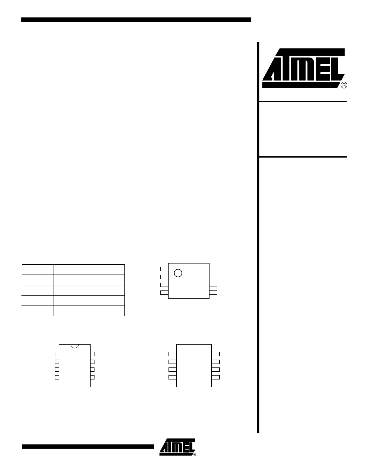
Pin Configurations
Pin Name Function
NC No Connect
SDA Serial Data
SCL Serial Clock Input
TEST Test Input (GND or VCC)
8-lead PDIP
NC
NC
NC
GND
8-lead TSSOP
1
2
3
4
8-lead SOIC
VCC
8
TEST
7
SCL
6
SDA
5
AT24C0 1
NC
NC
NC
GND
8
1
2
3
4
VCC
7
TEST
6
SCL
5
SDA
NC
NC
NC
GND
1
2
3
4
VCC
8
TEST
7
SCL
6
SDA
5
Rev. 0134E–SEEPR–08/02
1
Page 2
Absolute Maximum Ratings*
Operating Temperature .................................. -55°Cto+125°C
Storage Temperature ..................................... -65°Cto+150°C
Voltage on Any Pin
with Respect to Ground .....................................-1.0V to +7.0V
Maximum Operating Voltage .......................................... 6.25V
DC Output Current ........................................................ 5.0 mA
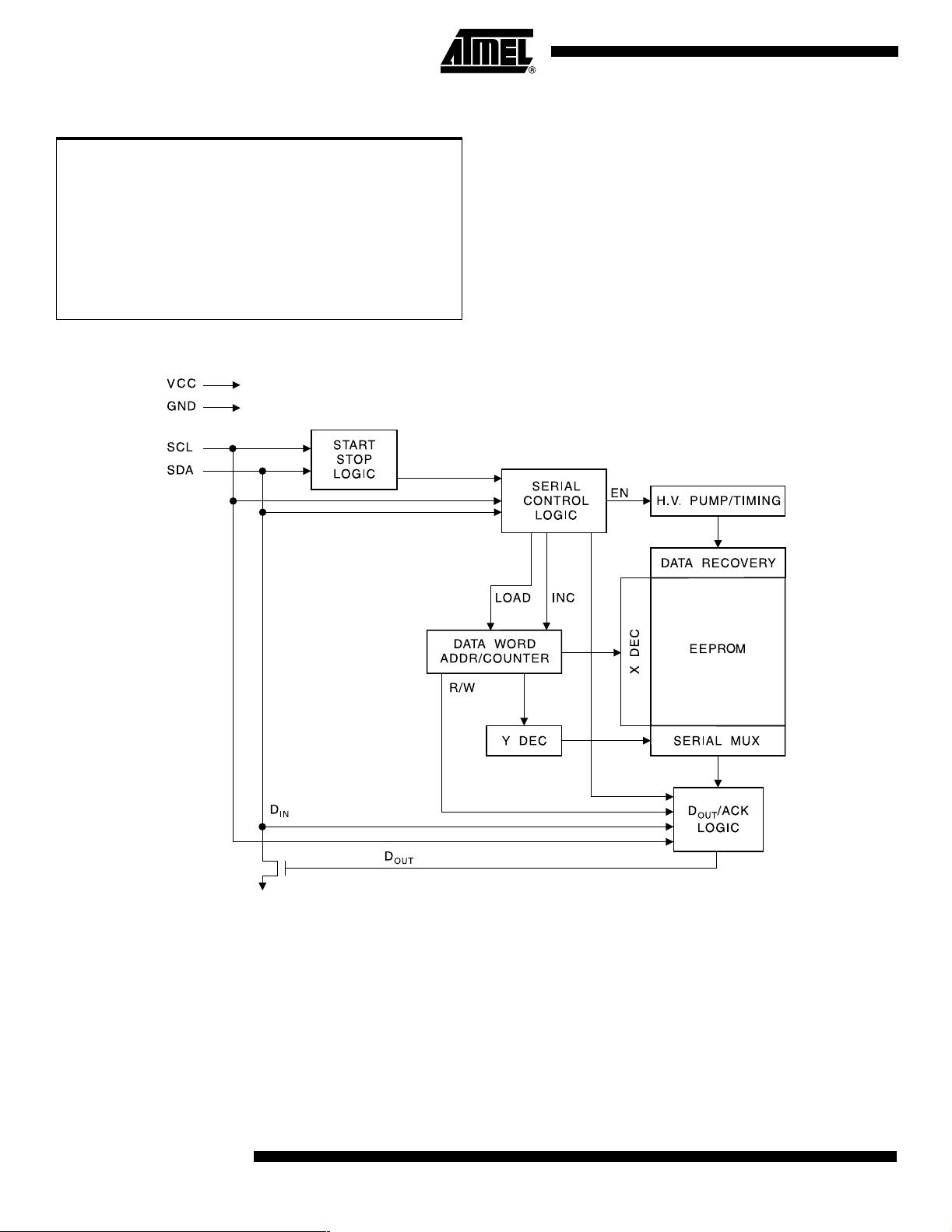
Block Diagram
*NOTICE: Stresses beyond those listed under “Absolute
Maximum Ratings” may cause permanent damage to the device. This is a stress rating only and
functional operation of the device at these or any
other conditions beyond those indicated in the
operational sections of this specification is not
implied. Exposure to absolute maximum rating
conditions for extended periods may affect
device reliability.
2
AT24C01
0134E–SEEPR–08/02
Page 3
AT24C01
Pin Description SERIAL CLOCK (SCL): The SCL input is used to positive edge clock data into each
EEPROM device and negative edge clock data out of each device.
SERIAL DATA (SDA): The SDA pin is bidirectional for serial data transfer. This pin is
open-drain driven and may be wire-ORed with any number of other open-drain or open
collector devices.
Memory Organization AT24C01, 1K SERIAL EEPROM: Internally organized with 128 pages of 1 byte each.
The 1K requires a 7-bit data word address for random word addressing.
Pin Capacitance
Applicable over recommended operating range from TA=25°C, f = 1.0 MHz, VCC= +1.8V.
Symbol Test Condition Max Units Condition
C
I/O
C
IN
Input/Output Capacitance (SDA) 8 pF V
Input Capacitance (A0, A1, A2, SCL) 6 pF VIN=0V
DC Characteristics
I/O
=0V
Applicable over recommended operating range from: TAI=-40°Cto+85°C, VCC= +1.8V to +5.5V, TAC=0°Cto+70°C,
V
= +1.8V to +5.5V (unless otherwise noted).
CC
Symbol Parameter Test Condition Min Typ Max Units
V
CC1
V
CC2
V
CC3
V
CC4
I
CC
I
CC
I
SB1
I
SB2
I
SB3
I
SB4
I
LI
I
LO
V
IL
V
IH
V
OL2
V
OL1
Note: 1. VILmin and VIHmax are reference only and are not tested.
Supply Voltage 1.8 5.5 V
Supply Voltage 2.5 5.5 V
Supply Voltage 2.7 5.5 V
Supply Voltage 4.5 5.5 V
Supply Current VCC= 5.0V READ at 100 kHz 0.4 1.0 mA
Supply Current VCC= 5.0V WRITE at 100 kHz 2.0 3.0 mA
Standby Current VCC=1.8V VIN=VCCor V
Standby Current VCC=2.5V VIN=VCCor V
Standby Current VCC=2.7V VIN=VCCor V
Standby Current VCC=5.0V VIN=VCCor V
Input Leakage Current VIN=VCCor V
Output Leakage Current V
Input Low Level
Input High Level
(1)
(1)
OUT=VCC
or V
SS
SS
SS
SS
SS
SS
-0.6 VCC× 0.3 V
VCC× 0.7 VCC+0.5 V
0.6 3.0 µA
1.4 4.0 µA
1.6 4.0 µA
8.0 18.0 µA
0.10 3.0 µA
0.05 3.0 µA
Output Low Level VCC=3.0V IOL=2.1mA 0.4 V
Output Low Level VCC=1.8V IOL=0.15mA 0.2 V
0134E–SEEPR–08/02
3
Page 4
AC Characteristics
Applicable over recommended operating range from TA=-40°Cto+85°C, VCC= +1.8V to +5.5V, CL = 1 TTL Gate and
100 pF (unless otherwise noted).
2.7-, 2.5-, 1.8-volt 5.0-volt
Symbol Parameter
f
SCL
t
LOW
t
HIGH
t
I
t
AA
t
BUF
t
HD.STA
t
SU.STA
t
HD.DAT
t
SU.DAT
t
R
t
F
t
SU.STO
t
DH
t
WR
Endurance
Clock Frequency, SCL 100 400 kHz
Clock Pulse Width Low 4.7 1.2 µs
Clock Pulse Width High 4.0 0.6 µs
Noise Suppression Time
(1)
Clock Low to Data Out Valid 0.1 4.5 0.1 0.9 µs
Time the bus must be free before a new
transmission can start
(1)
Start Hold Time 4.0 0.6 µs
Start Set-up Time 4.7 0.6 µs
Data In Hold Time 0 0 µs
Data In Set-up Time 200 100 ns
Inputs Rise Time
Inputs Fall Time
(1)
(1)
Stop Set-up Time 4.7 0.6 µs
Data Out Hold Time 100 50 ns
WriteCycleTime 10 10 ms
(1)
5.0V, 25°C, Page Mode 1M 1M
Note: 1. This parameter is characterized and is not 100% tested.
UnitsMin Max Min Max
100 50 ns
4.7 1.2 µs
1.0 0.3 µs
300 300 ns
Write
Cycles
4
AT24C01
0134E–SEEPR–08/02
Page 5

AT24C01
Device Operation CLOCK and DATA TRANSITIONS: The SDA pin is normally pulled high with an exter-
nal device. Data on the SDA pin may change only during SCL low time periods (refer to
Data Validity timing diagram). Data changes during SCL high periods will indicate a start
or stop condition as defined below.
START CONDITION: A high-to-low transition of SDA with SCL high is a start condition
which must precede any other command (refer to Start and Stop Definition timing
diagram).
STOP CONDITION: A low-to-high transition of SDA with SCL high is a stop condition
which terminates all communications. After a read sequence, the stop command will
place the EEPROM in a standby power mode (refer to Start and Stop Definition timing
diagram).
ACKNOWLEDGE: All addresses and data words are serially transmitted to and from
the EEPROM in 8-bit words. Any device on the system bus receiving data (when communicating with the EEPROM) must pull the SDA bus low to acknowledge that it has
successfully received each word. This must happen during the ninth clock cycle after
each word received and after all other system devices have freed the SDA bus. The
EEPROM will likewise acknowledge by pulling SDA low after receiving each address or
data word (refer to Acknowledge Response from Receiver timing diagram).
STANDBY MODE: The AT24C01 features a low power standby mode which is enabled:
(a) upon power-up and (b) after the receipt of the STOP bit and the completion of any
internal operations.
MEMORY RESET: After an interruption in protocol, power loss or system reset, any 2wire part can be reset by following these steps:
(a) Clock up to 9 cycles, (b) look for SDA high in each cycle while SCL is high and then
(c) create a start condition as SDA is high.
0134E–SEEPR–08/02
5
Page 6

Bus Timing SCL: Serial Clock, SDA: Serial Data I/O
Write Cycle Timing SCL: Serial Clock, SDA: Serial Data I/O
SCL
SDA
Note: 1. The write cycle time tWRis the time from a valid stop condition of a write sequence to the end of the internal clear/write cycle.
8th BIT ACK
WORD n
STOP
CONDITION
t
(1)
WR
START
CONDITION
6
AT24C01
0134E–SEEPR–08/02
Page 7

Data Validity
Start and Stop Definition
AT24C01
Output Acknowledge
0134E–SEEPR–08/02
7
Page 8

Write Operations BYTE WRITE: Following a start condition, a write operation requires a 7-bit data word
address and a low write bit. Upon receipt of this address, the EEPROM will again
respond with a zero and then clock in the first 8-bit data word. Following receipt of the 8bit data word, the EEPROM will output a zero and the addressing device, such as a
microcontroller, must terminate the write sequence with a stop condition. At this time the
EEPROM enters an internally-timed write cycle to the nonvolatile memory. All inputs are
disabled during this write cycle , t
complete (refer to Figure 1).
PAG E WR I TE : The AT24C01 is capable of a 4-byte page write.
A page write is initiated the same as a byte write but the microcontroller does not send a
stop condition after the first data word is clocked in. Instead, after the EEPROM
acknowledges receipt of the first data word, the microcontroller can transmit up to three
more data words. The EEPROM will respond with a zero after each data word received.
The microcontroller must terminate the page write sequence with a stop condition (refer
to Figure 2).
The data word address lower 2 bits are internally incremented following the receipt of
each data word. The higher five data word address bits are not incremented, retaining
the memory page row location. When the word address, internally generated, reaches
the page boundary, the following byte is placed at the beginning of the same page. If
more than four data words are transmitted to the EEPROM, the data word address will
“roll over” and previous data will be overwritten.
ACKNOWLEDGE POLLING: Once the internally-timed write cycle has started and the
EEPROM inputs are disabled, acknowledge polling can be initiated. This involves sending a start condition followed by the device address word. The read/write bit is
representative of the operation desired. Only if the internal write cycle has completed
will the EEPROM respond with a zero allowing the read or write sequence to continue.
, and the EEPROM will not respond until the write is
WR
Read Operations Read operations are initiated the same way as write operations with the exception that
the read/write select bit in the device address word is set to one. There are two read
operations: byte read and sequential read.
BYTE READ: A byte read is initiated with a start condition followed by a 7-bit data word
address and a high read bit. The AT24C01 will respond with an acknowledge and then
serially output 8 data bits. The microcontroller does not respond with a zero but does
generate a following stop condition (refer to Figure 3).
SEQUENTIAL READ: Sequential reads are initiated the same as a byte read. After the
microcontroller receives an 8-bit data word, it responds with an acknowledge. As long as
the EEPROM receives an acknowledge, it will continue to increment the data word
address and serially clock out sequential data words. When the memory address limit is
reached, the data word address will “roll over” and the sequential read will continue. The
sequential read operation is terminated when the microcontroller does not respond with
an input zero but does generate a following stop condition (refer to Figure 4).
8
AT24C01
0134E–SEEPR–08/02
Page 9
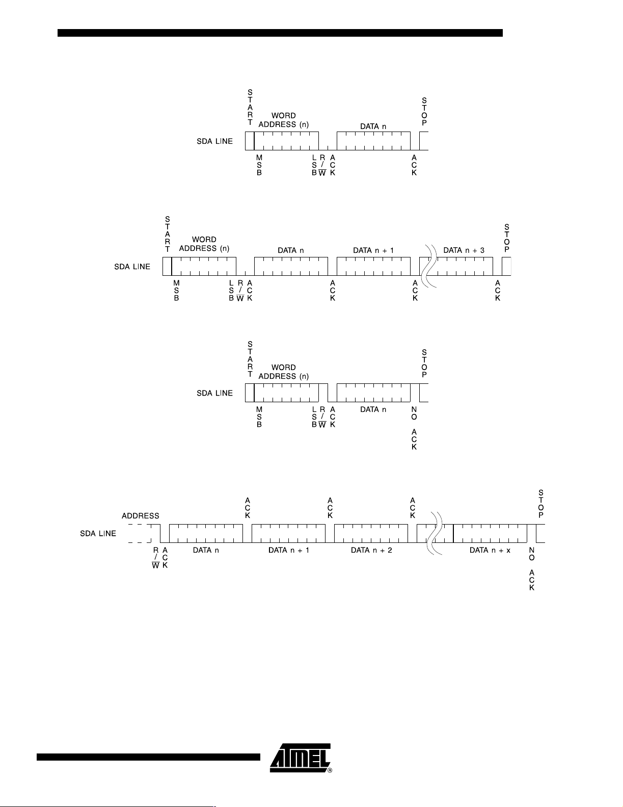
Figure 1. Byte Write
Figure 2. Page Write
Figure 3. Byte Read
AT24C01
Figure 4. Sequential Read
0134E–SEEPR–08/02
9
Page 10
Ordering Information
Ordering Code Package Operation Range
AT24C01-10PI-2.7
AT24C01-10SI-2.7
AT24C01-10TI-2.7
AT24C01-10PI-1.8
AT24C01-10SI-1.8
AT24C01-10TI-1.8
Note: For 2.7V devices used in the 4.5V to 5.5V range, please refer to performance values in the AC and DC Characteristics tables.
8P3
8S1
8A2
8P3
8S1
8A2
Industrial
(-40°Cto85°C)
Industrial
(-40°Cto85°C)
Package Type
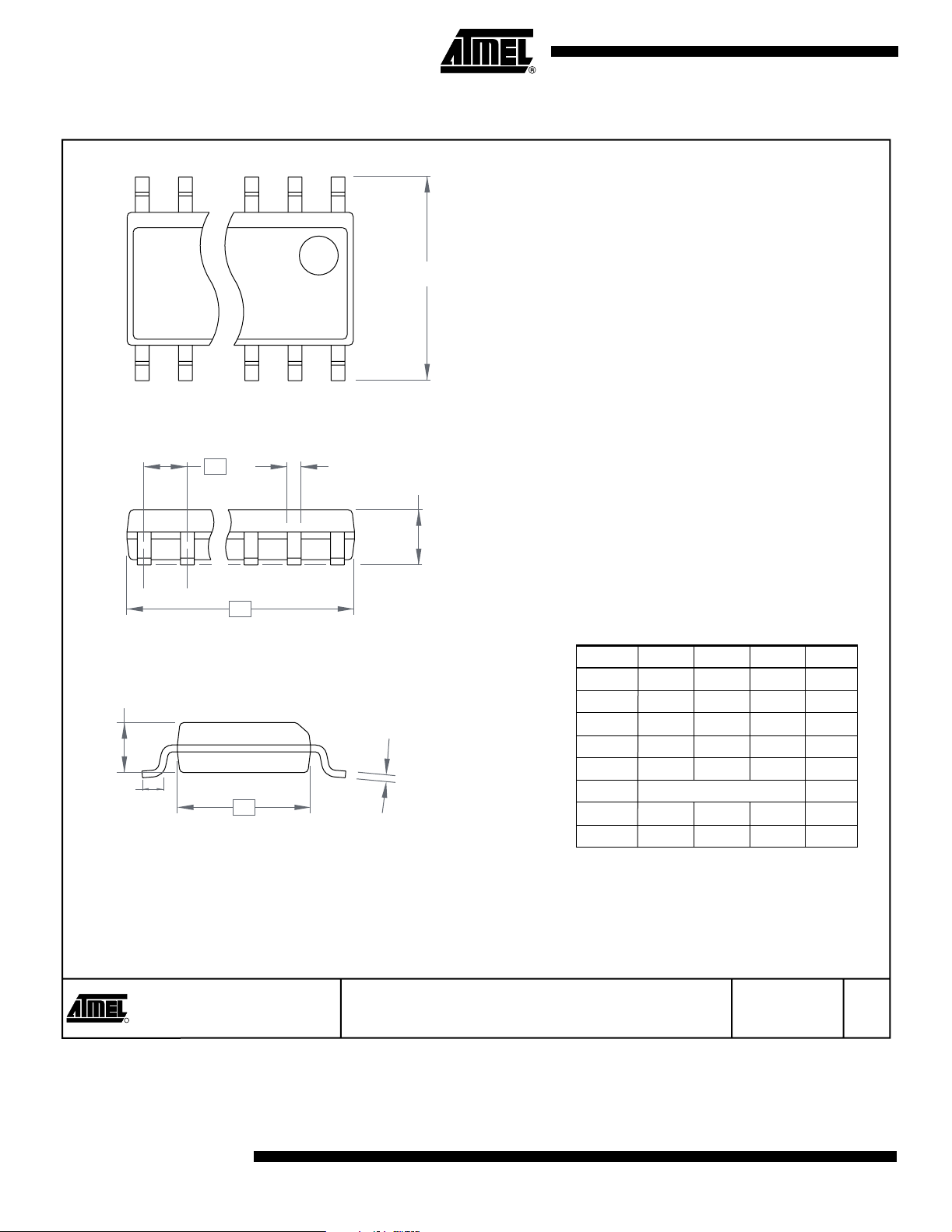
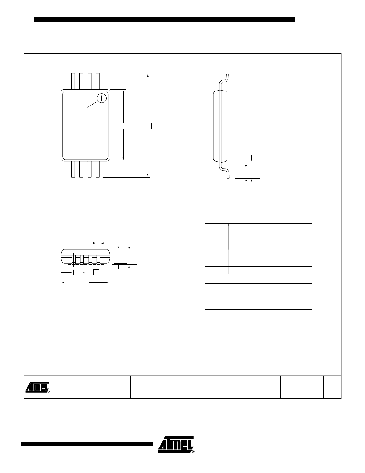
8P3 8-lead, 0.300" Wide, Plastic Dual Inline Package (PDIP)
8S1 8-lead, 0.150" Wide, Plastic Gull Wing Small Outline (JEDEC SOIC)
8A2 8-lead, 0.170" Wide, Thin Shrink Small Outline Package (TSSOP)
Options
-2.7 Low-Voltage (2.7V to 5.5V)
-1.8 Low-Voltage (1.8V to 5.5V)
10
AT24C01
0134E–SEEPR–08/02
Page 11

Packaging Information
8P3 – PDIP
AT24C01
D1
b3
4 PLCS
Top View
D
e
Side View
1
E
E1
N
c
eA
End View
COMMON DIMENSIONS
(Unit of Measure = inches)
b
b2
A2 A
SYMBOL
A 0.210 2
A2 0.115 0.130 0.195
b 0.014 0.018 0.022 5
b2 0.045 0.060 0.070 6
b3 0.030 0.039 0.045 6
c 0.008 0.010 0.014
D 0.355 0.365 0.400 3
L
D1 0.005 3
E 0.300 0.310 0.325 4
E1 0.240 0.250 0.280 3
e 0.100 BSC
eA 0.300 BSC 4
L 0.115 0.130 0.150 2
MIN
NOM
MAX
NOTE
Notes: 1. This drawing is for general information only; refer to JEDEC Drawing MS-001, Variation BA for additional information.
0134E–SEEPR–08/02
2. Dimensions A and L are measured with the package seated in JEDEC seating plane Gauge GS-3.
3. D, D1 and E1 dimensions do not include mold Flash or protrusions. Mold Flash or protrusions shall not exceed 0.010 inch.
4. E and eA measured with the leads constrained to be perpendicular to datum.
5. Pointed or rounded lead tips are preferred to ease insertion.
6. b2 and b3 maximum dimensions do not include Dambar protrusions. Dambar protrusions shall not exceed 0.010 (0.25 mm).
TITLE
2325 Orchard Parkway
R
San Jose, CA 95131
8P3, 8-lead, 0.300" Wide Body, Plastic Dual
In-line Package (PDIP)
DRAWING NO.
8P3
01/09/02
REV.
B
11
Page 12
8S1 – JEDEC SOIC
Top View
1
2
3
H
N
A2
L
e
D
Side View
E
End View
B
A
COMMON DIMENSIONS
(Unit of Measure = mm)
SYMBOL
A – – 1.75
B – – 0.51
C
C – – 0.25
D – – 5.00
E – – 4.00
e 1.27 BSC
H – – 6.20
L – – 1.27
MIN
NOM
MAX
NOTE
12
Note:
This drawing is for general information only. Refer to JEDEC Drawing MS-012 for proper dimensions, tolerances, datums, etc.
TITLE
2325 Orchard Parkway
R
San Jose, CA 95131
8S1, 8-lead (0.150" Wide Body), Plastic Gull Wing
Small Outline (JEDEC SOIC)
AT24C01
DRAWING NO.
8S1 A
0134E–SEEPR–08/02
10/10/01
REV.
Page 13
8A2 – TSSOP
Pin 1 indicator
this corner
AT24C01
123
N
Top View
b
e
D
Side View
A2
E1
E
L1
L
End View
COMMON DIMENSIONS
(Unit of Measure = mm)
SYMBOL
A
D 2.90 3.00 3.10 2, 5
E 6.40 BSC
E1 4.30 4.40 4.50 3, 5
A ––1.20
A2 0.80 1.00 1.05
b 0.19 – 0.30 4
e 0.65 BSC
L 0.45 0.60 0.75
L1 1.00 REF
MIN
NOM
MAX
NOTE
Notes: 1. This drawing is for general information only. Refer to JEDEC Drawing MO-153, Variation AA, for proper dimensions, tolerances,
0134E–SEEPR–08/02
datums, etc.
2. Dimension D does not include mold Flash, protrusions or gate burrs. Mold Flash, protrusions and gate burrs shall not exceed
0.15 mm (0.006 in) per side.
3. Dimension E1 does not include inter-lead Flash or protrusions. Inter-lead Flash and protrusions shall not exceed 0.25 mm
(0.010 in) per side.
4. Dimension b does not include Dambar protrusion. Allowable Dambar protrusion shall be 0.08 mm total in excess of the
b dimension at maximum material condition. Dambar cannot be located on the lower radius of the foot. Minimum space between
protrusion and adjacent lead is 0.07 mm.
5. Dimension D and E1 to be determined at Datum Plane H.
2325 Orchard Parkway
R
San Jose, CA 95131
TITLE
8A2, 8-lead, 4.4 mm Body, Plastic
Thin Shrink Small Outline Package (TSSOP)
DRAWING NO.
8A2
5/30/02
REV.
B
13
Page 14

Atmel Headquarters Atmel Operations
Corporate Headquarters
2325 Orchard Parkway
San Jose, CA 95131
TEL 1(408) 441-0311
FAX 1(408) 487-2600
Europe
Atmel Sarl
Route des Arsenaux 41
Case Postale 80
CH-1705 Fribourg
Switzerland
TEL (41) 26-426-5555
FAX (41) 26-426-5500
Asia
Room 1219
Chinachem Golden Plaza
77 Mody Road Tsimshatsui
East Kowloon
Hong Kong
TEL (852) 2721-9778
FAX (852) 2722-1369
Japan
9F, Tonetsu Shinkawa Bldg.
1-24-8 Shinkawa
Chuo-ku, Tokyo 104-0033
Japan
TEL (81) 3-3523-3551
FAX (81) 3-3523-7581
Memory
2325 Orchard Parkway
San Jose, CA 95131
TEL 1(408) 441-0311
FAX 1(408) 436-4314
Microcontrollers
2325 Orchard Parkway
San Jose, CA 95131
TEL 1(408) 441-0311
FAX 1(408) 436-4314
La Chantrerie
BP 70602
44306 Nantes Cedex 3, France
TEL (33) 2-40-18-18-18
FAX (33) 2-40-18-19-60
ASIC/ASSP/Smart Cards
Zone Industrielle
13106 Rousset Cedex, France
TEL (33) 4-42-53-60-00
FAX (33) 4-42-53-60-01
1150 East Cheyenne Mtn. Blvd.
Colorado Springs, CO 80906
TEL 1(719) 576-3300
FAX 1(719) 540-1759
Scottish Enterprise Technology Park
Maxwell Building
East Kilbride G75 0QR, Scotland
TEL (44) 1355-803-000
FAX (44) 1355-242-743
RF/Automotive
Theresienstrasse 2
Postfach 3535
74025 Heilbronn, Germany
TEL (49) 71-31-67-0
FAX (49) 71-31-67-2340
1150 East Cheyenne Mtn. Blvd.
Colorado Springs, CO 80906
TEL 1(719) 576-3300
FAX 1(719) 540-1759
Biometrics/Imaging/Hi-Rel MPU/
High Speed Converters/RF Datacom
Avenue de Rochepleine
BP 123
38521 Saint-Egreve Cedex, France
TEL (33) 4-76-58-30-00
FAX (33) 4-76-58-34-80
e-mail
literature@atmel.com
Web Site
http://www.atmel.com
© Atmel Corporation 2002.
Atmel Corporation makes no warranty for the use of its products, other than those expressly contained in the Company’s standard warranty
whichisdetailedinAtmel’s Terms and Conditions located on the Company’s web site. The Company assumes no responsibility for any errors
which may appear in this document, reserves the right to change devices or specifications detailed herein at any time without notice, and does
not make any commitment to update the information contained herein. No licenses to patents or other intellectual property of Atmel are granted
by the Company in connection with the sale of Atmel products, expressly or by implication. Atmel’s products are not authorized for use as critical
components in life support devices or systems.
AT ME L®is the registered trademark of Atmel.
Other terms and product names may be the trademarks of others.
Printed on recycled paper.
0134E–SEEPR–08/02 xM
 Loading...