

Page 1
Features
• Low-voltage Programmable Logic Device
– Wide Power Supply Range - 3.0V to 5.5V
– Ideal for Battery Powered Systems
• High-speed Operation
– 20 ns Maximum Propagation Delay at V
CC
= 3.0V
• Commercial and Industrial Temperature Ranges
• Familiar 22V10 Logic Architecture
• Low-power 3-volt CMOS Operation
AT22LV10L AT22LV10
Temp Com./Ind. Com./Ind.
I
(mA) 4/5 35/45 VCC = 3.6V
CC
• CMOS and TTL Compatible Inputs and Outputs
– 10 µA Leakage Maximum
• Reprogrammable – Tested 100% for Programmability
• High-reliability CMOS Technology
– 2000V ESD Protection
– 200 mA Latchup Immunity
• Dual-in-line and Surface Mount Packages
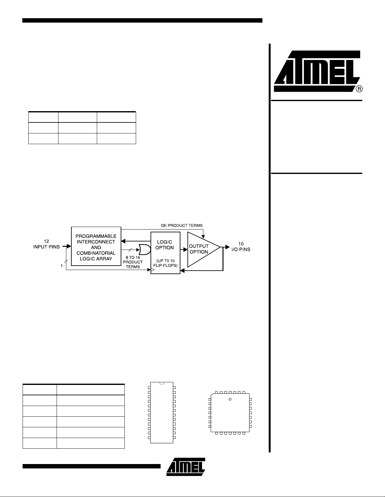
Logic Diagram
Low-voltage UV
Erasable
Programmable
Logic Device
AT22LV10
AT22LV10L
Description
The AT22LV10 and AT22LV10 L are low-vo lta ge compatible CMOS high-per forma nc e
Programmable Logic Devices (PLDs). Speeds down to 20 ns and po wer dissipation
as low as 14.4 mW ar e offered . All sp eed rang es are spe cifi ed over th e 3.0V to 5. 5V
range. All pins offer a low
±10 µA leakage.
The AT22LV10L provides the optimum low-power CMOS PLD solution, with low DC
power (1 mA typical at V
= 3.3V) and full CMOS output levels. The AT22LV10L
CC
significantly reduces total system power, allowing battery powered operation.
(continued)
Pin Configurations
All Pinouts Top View
Pin Name Function
CLK/IN Clock and Logic Input
IN Logic Inputs
I/O Bidirectional Buffe rs
* No Internal Connection
VCC 3.0V to 5.5V Supply
DIP/SOIC PLCC
1
CLK/IN
GND
IN
IN
IN
IN
IN
IN
IN
IN
IN
IN
24
2
3
4
5
6
7
8
9
10
11
12
VCC
23
I/O
22
I/O
21
I/O
20
I/O
19
I/O
18
I/O
17
I/O
16
I/O
15
I/O
14
I/O
13
IN
IN
IN
IN
*
IN
IN
IN
ININCLK/IN*VCC
432
5
6
7
8
9
10
11
1
12131415161718
*
IN
IN
GND
I/O
282726
IN
I/O
I/O
I/O
25
I/O
24
I/O
23
*
22
I/O
21
I/O
20
I/O
19
I/O
Rev. 0190E–08/99
1
Page 2
Full CMOS output levels help reduce power in many other
system components.
The AT22LV10 and AT22LV10L logic architectures are
identical to the familiar 22V10. Each output is allocated
from eight to 16 product terms, whi ch allows highly
complex logic functions to be realized.
Two additional product terms are included to provide
synchronous preset and asynchronous reset. These terms
are common to all ten registers. All registers are automatically cleared upon power-up.
Register pr el o ad sim p li fi e s te s ti n g. A se cu rity fuse prev ent s
unauthorized copying of programmed fuse patterns.
Absolute Maximum Ratings*
Temperature Under Bias................................ -55°C to +125°C
Storage Temperature..................................... -65°C to +150°C
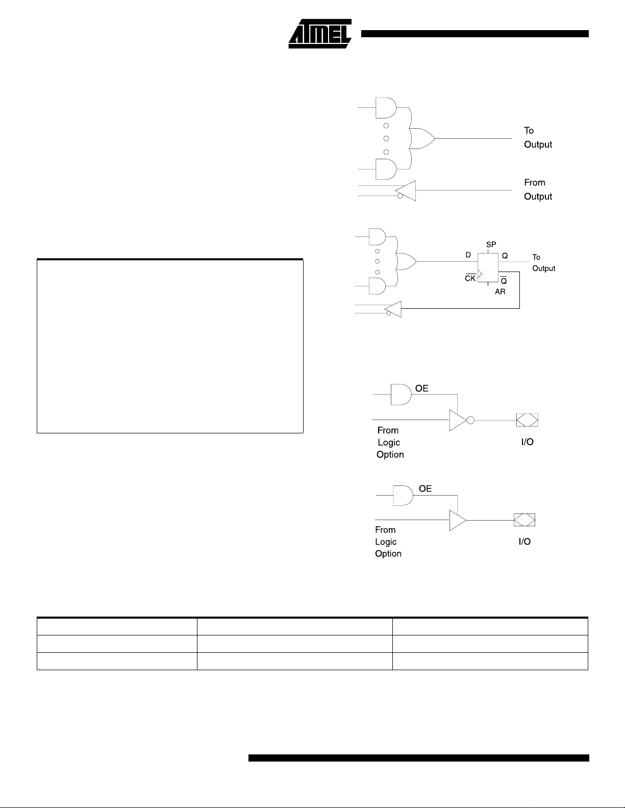
Logic Options
Voltage on Any Pin with
Respect to Ground ........................................-2.0V to +7.0V
Voltage on Input Pins
with Respect to Ground
During Programming....................................-2.0V to +14.0V
Programming Voltage with
Respect to Ground ......................................-2.0V to +14.0V
Integrated UV Erase Dose..............................7258 W•sec/cm
*NOTICE: Stresses beyond those listed under “Absolute Maxi-
mum Ratings” may cause permanent dama ge to the
device. This is a stress rating only and functional
operation of the device at these or any other conditions beyond those indicated in the operational
sections of this specification is not implied. Exposure to absolute maximum rating conditions for
extended periods may affect device reliability.
Note: 1. Minimum voltage is -0.6 V DC whic h ma y undershoot
to -2.0V for pulses of less than 20 ns. Maximum pin
voltage is V
+ 2.0V for pulses of less than 20 ns.
V
CC
+ 0.75V DC which may undershoot to
CC
(1)
(1)
(1)
2
Output Options
DC and AC Operating Conditions
Commercial Industrial
Operating Temperature (Ambient) 0°C - 70°C-40°C - 85°C
V
Power Supply 3.0V to 5.5V 3.0V to 5.5V
CC
2
AT22LV10(L)
Page 3
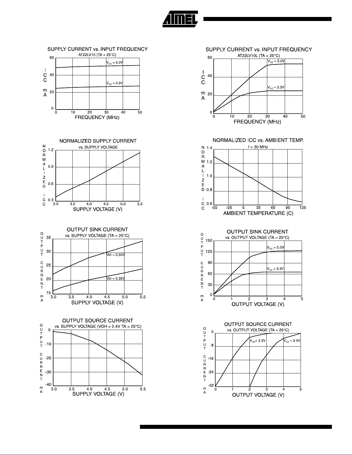
DC Characteristics
Symbol Parameter Condition
I
LI
I
LO
I
CC
Input Load Current VIN = -0.1V to VCC + 1V 10 µA
Output Leakage
Current
Power Supply
Current
= -0.1V to VCC + 0.1V 10 µA
V
OUT
= 3.6V/5.5V,
V
CC
= GND,
V
IN
Outputs Open
AT22LV10(L)
(2)
Com. 20/50 35/90 mA
AT22LV10
Ind. 20/50 45/100 mA
Com. 1/2 4/12 mA
AT22LV10L
Ind. 1/2 5/15 mA
Min Typ Max Units
(1)
I
OS
V
IL1
V
IL2
V
IH
Output Short Circuit
Current
Input Low Voltage 4.5V ≤ V
Input Low Voltage 3.0V ≤ V
= 0.5V -120 mA
V
OUT
5.5V -0.6 0.8 V
CC ≤
4.5V -0.6 0.6 V
CC <
Input High Voltage 2.0 V
+ 0.75 V
CC
VCC = 3.0V Com., Ind. IOL = 8 mA 0.5 V
V
OL
V
OH
Output Low Voltage
= VIH or V
V
IN
IL
Output High Voltage
V
= 4.5V Com., Ind. IOL = 16 mA 0.5 V
CC
V
= 3.0V Com., Ind. IOL = 6 mA 0.35 V
CC
= VIH or VIL,
V
IN
= 3.0V/4.5V
V
CC
IOH = -100 µA V
I
= -0.4 mA/-4.0 mA 2.4 V
OH
- 0.3 V
CC
Notes: 1. Not more than one output at a time should be shorted. Duration of short circuit test should not exceed 30 sec.
2. For DC characteristics, the test condition of V
= Max corresponds to 3.6V.
CC
3
Page 4
AC Characteristics for the AT22LV10
Symbol Parameter
AT22LV10-20 AT22LV10-25
UnitsMin Typ Max Min Typ Max
t
PD
t
EA
t
ER
t
CF
t
CO
t
S
t
H
t
P
t
W
Input or Feedback to NonRegistered Output
12 20 15 25 ns
Input to Output Enable 20 15 25 ns
Input to Output Disable 20 15 25 ns
Clock to Feedback 049059ns
Clock to Output 0 8 14 0 10 17 ns
Input or Feedback Setup Time 10 6 12 7 ns
Hold Time 0 0 ns
Clock Period 10 12 ns
Clock Width 5 6 ns
External Feedback 1/(tS+tCO) 41.6 34.5 MHz
F
MAX
t
AW
Internal Feedback 1/(tS + tCF) 52.6 47.6 MHz
No Feedback 1/(t
) 100.0 83.3 MHz
P
Asynchronous Reset Width 20 12 25 15 ns
Asynchronous Reset,
t
AR
Synchronous Preset,
20 12 25 15 ns
Recovery Time
t
AP
Asynchronous Reset to
Registered Output Res et
15 25 18 28 ns
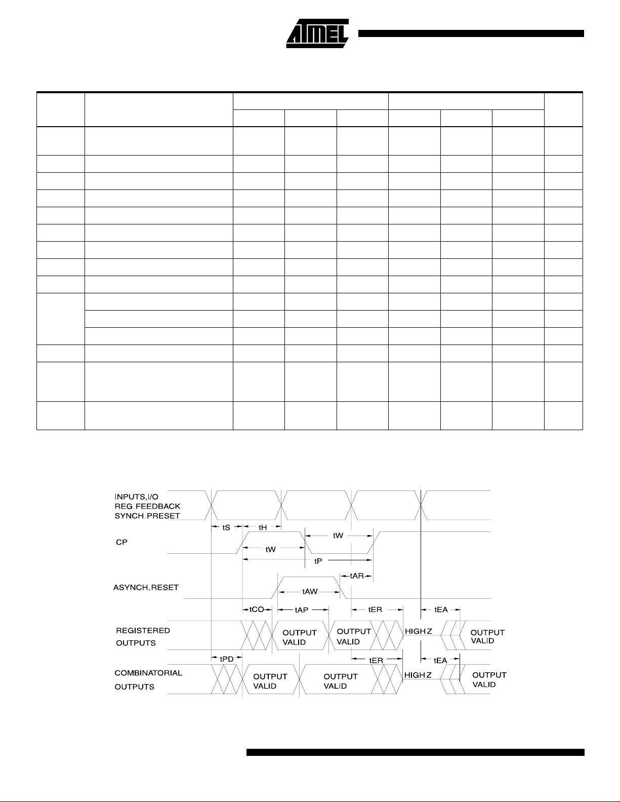
AC Waveforms
(1)
Note: 1. Timing measurement reference is 1.5V. Input AC driving levels are 0.0V and 3.0V, unless otherwise specified.
4
AT22LV10(L)
Page 5

AC Characteristics for the AT22LV10L
Symbol Parameter
AT22LV10(L)
AT22LV10L-25
UnitsMin Typ Max
t
PD
t
EA
t
ER
t
CF
t
CO
t
SF
t
S
t
H
t
P
t
W
Input or Feedback to Non-Registered Output 15 25 ns
Input to Output Enable 15 25 ns
Input to Output Disable 15 25 ns
Clock to Feedback 0 5 9 ns
Clock to Output 0 10 14 ns
Feedback Setup T im e 12 7 ns
Input Setup Time 17 15 ns
Hold Time 0 ns
Clock Period 12 ns
Clock Width 6 ns
External Feedback 1/(tS + tCO)32.2MHz
F
MAX
t
AW
t
AR
t
AP
Internal Feedback 1/(t
No Feedback 1/(t
+ tCF)47.6MHz
SF
) 83.3 MHz
P
Asynchronous Reset Width 25 15 ns
Asynchronous Reset Recovery Time 25 15 ns
Asynchronous Reset to Registered Output Reset 18 28 ns
Input Test Waveforms and
Output Test Loads
Measurement Levels
Commercial
5
Page 6

Functional Logic Diagram AT22LV10(L)
6
AT22LV10(L)
Page 7
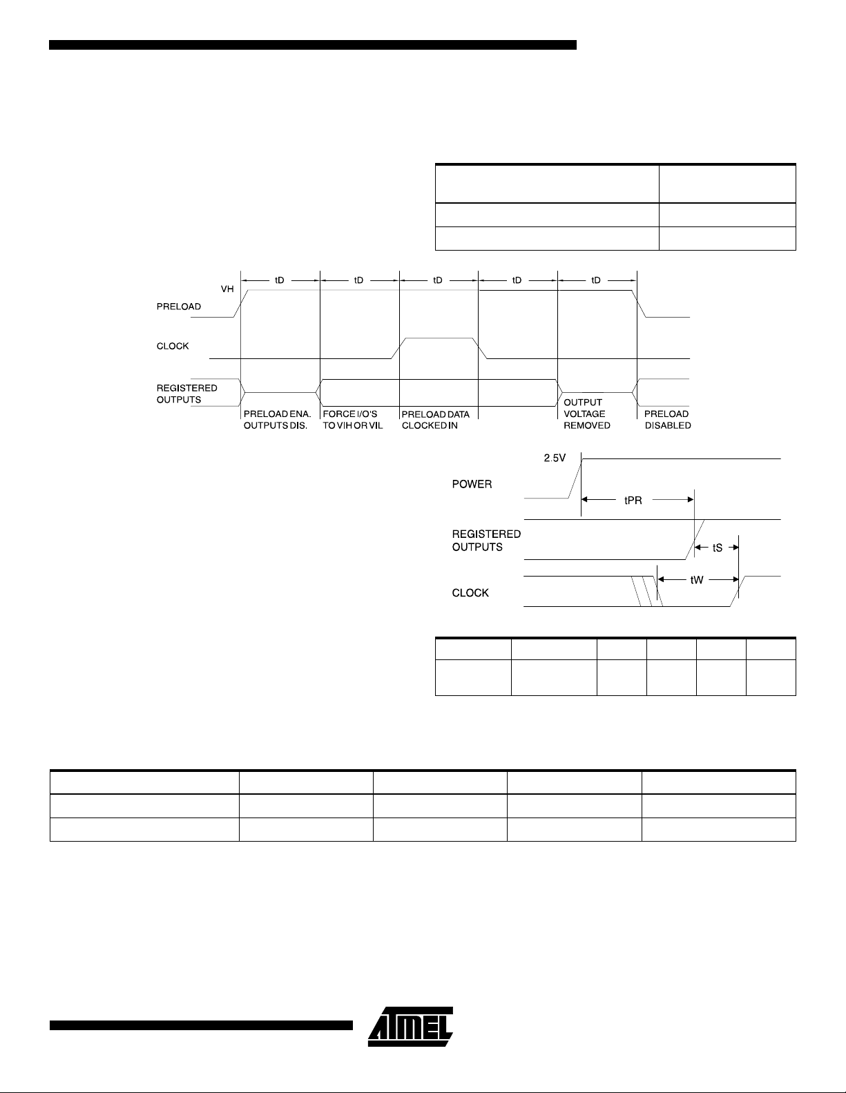
Preload of Registered Outputs
AT22LV10(L)
The registers in the AT22LV10 and AT22LV10L are provided with circuitry to allow loading of each register
asynchronously wi th eit her a hig h or a lo w. Th is f eatu re will
simplify testing since any state can be forced into the registers to control test sequencing. A V
will force the register high; a V
IL
level on the I/O pin
IH
will force it low, indep endent of the p olarity b it (C0) setting. The prel oad stat e is
entered by placing an 11.5V to 13V signal on pin 8 on
Power-up Reset
The registers in the AT22LV10 and AT22LV10L are
designed to reset during power-up. At a point delayed
slightly from V
the low state. The output state will depend on the polarity of
the output buffer.
This feature is critical for state machine initialization.
However, due to the asynchronous nature of reset and the
uncertainty of how V
following conditions are required:
1. The V
2. After reset occurs, all input and feedback setup
times must be met before driving the clock pin high,
and
3. The clock must remain stable during t
crossing 2.5V, all registers wil l be reset to
CC
actually rises in the system, the
CC
rise must be monotonis;
CC
.
PR
DIPs, and pin 10 on SMPs. When the clock pin is pulsed
high, the data on the I/O pins is placed into the ten
registers.
Level Forced on Registe red Output
Pin During Preload Cycle
V
IH
V
IL
Parameter Description Min Typ Max Units
t
PR
Power-up
Reset Time
Register State After
Cycle
High
Low
600 1000 ns
Pin Capacitance
(f = 1 MHz, T = 25°C)
C
IN
C
OUT
Note: 1. Typical values for nominal supply voltage. This parameter is only sampled and is not 100% tested.
(1)
Typ Max Units Conditions
58pFV
68pFV
Erasure Characteristics
The entire fuse array of an AT22LV10 or AT22LV10L is
erased after exposure to ultra violet ligh t at a wav elen gth of
2537 Å. Complete erasure is assured after a minimum of
20 minutes exposu re usin g 12,000 µW/cm
2
intensity lamps
spaced one inch away from the chip. Minimum erase time
for lamps at other intensity ratings can be calculated fro m
the minimum in tegrated erasu re dose of 15 W
prevent unintentional erasure, an opaque label is recommended to cover the clear window on any UV erasable
PLD which will be subjected to continuous fluorescent
indoor lighting or sunligh t.
= 0V
IN
OUT
= 0V
•sec/cm
2
. To
7
Page 8
8
AT22LV10(L)
Page 9

AT22LV10(L)
9
Page 10

Ordering Information
t
PD
(ns)
20 10 14 AT22LV10-20JC
25 12 17 AT22LV10-25JC
25 17 14 AT22LV10L-25JC
t
S
(ns)
t
CO
(ns) Ordering Code Package Operation Range
AT22LV10-20PC
AT22LV10-20SC
AT22LV10-20JI
AT22LV10-20PI
AT22LV10-20SI
AT22LV10-25PC
AT22LV10-25SC
AT22LV10-25JI
AT22LV10-25PI
AT22LV10-25SI
AT22LV10L-25PC
AT22LV10L-25SC
AT22LV10L-25JI
AT22LV10L-25PI
AT22LV10L-25SI
Using “C” Product for Industrial
28J
24P3
24S
28J
24P3
24S
28J
24P3
24S
28J
24P3
24S
28J
24P3
24S
28J
24P3
24S
Commercial
(0°C to 70°C)
Industrial
(-40°C to 85°C)
Commercial
(0°C to 70°C)
Industrial
(-40°C to 85°C)
Commercial
(0°C to 70°C)
Industrial
(-40°C to 85°C)
To use commercial product for Industrial temperature ranges, down-grade one speed grade from the “I” to the “C” device
(7 ns “C” = 10 ns “I”) and de-rate power by 30%.
Package Type
28J 28-lead, Plastic J-leaded Chip Carrier OTP (PLCC)
24P3 24-lead, 0.300" Wide, Plastic Dual Inline Package OTP (PDIP)
24S 24-lead, 0.300" Wide, Plastic Gull-Wing Small Outline OTP (SOIC)
10
AT22LV10(L)
Page 11

Packaging Information
.045(1.14) X 45°
PIN NO.1
IDENTIFY
.032(.813)
.026(.660)
.050(1.27) TYP
.300(7.62) REF SQ
.045(1.14) X 30° - 45°
.022(.559) X 45° MAX (3X)
.012(.305)
.008(.203)
.021(.533)
.013(.330)
.430(10.9)
.390(9.91)
SQ
.043(1.09)
.020(.508)
.120(3.05)
.090(2.29)
.180(4.57)
.165(4.19)
.456(11.6)
.450(11.4)
.495(12.6)
.485(12.3)
SQ
SQ
AT22LV10(L)
28J, 28-lead, Plastic J-leaded Chip Carrier (PLCC)
Dimensions in Inches and (Millimeters)
JEDEC STANDARD MS-018 AB
24P3, 24-lead, 0.300” Wide. Plastic
Dual Inline Package (PDIP)
Dimensions in Inches and (Millimeters)
JEDEC STANDARD MS-011 AB
1.27(32.3)
.200(5.06)
SEATING
PLANE
MAX
.151(3.84)
.125(3.18)
.110(2.79)
.090(2.29)
.012(.305)
.008(.203)
1.25(31.7)
1.100(27.94) REF
PIN
1
.065(1.65)
.040(1.02)
.325(8.26)
.300(7.62)
0
REF
15
.400(10.2) MAX
.023(.584)
.014(.356)
.266(6.76)
.250(6.35)
.090(2.29)
MAX
.005(.127)
MIN
.070(1.78)
.020(.508)
24S, 24-lead, 0.300” Wide, Plastic Gull-Wing Small
Outline (SOIC)
Dimensions in Inches and (Millimeters)
.020(.508)
.013(.330)
PIN 1 ID
.050(1.27) BSC
.616(15.6)
.598(15.2)
.012(.305)
.003(.076)
.050(1.27)
.015(.381)
0
REF
8
.299(7.60)
.291(7.39)
.420(10.7)
.393(9.98)
.105(2.67)
.092(2.34)
.013(.330)
.009(.229)
11
Page 12

Atmel Headquarters Atmel Operations
Corporate Headquarters
2325 Orchard Parkway
San Jose, CA 95131
TEL (408) 441- 0311
FAX (408) 487-2600
Europe
Atmel U.K., Ltd.
Coliseum Business Centre
Riverside Way
Camberley, Surrey GU15 3YL
England
TEL (44) 1276-686-677
FAX (44) 1276-686-697
Asia
Atmel Asia, Ltd.
Room 1219
Chinachem Golden Plaza
77 Mody Road Tsimhatsui
East Kowloon
Hong Kong
TEL (852) 2721- 9778
FAX (852) 2722-1369
Japan
Atmel Japan K.K.
9F, Tonetsu Shinkawa Bldg.
1-24-8 Shinka wa
Chuo-ku, Tokyo 104-0033
Japan
TEL (81) 3-3523-3551
FAX (81) 3-3523-7581
Atmel Colorado Springs
1150 E. Cheyenne Mtn. Blvd.
Colorado Springs, CO 80906
TEL (719) 576-3300
FAX (719) 540-1759
Atmel Rousset
Zone Indus triel le
13106 Rousset Cedex
France
TEL (33) 4-4253-6000
FAX (33) 4-4253-6001
Fax-on-Demand
North America:
1-(800) 292-8635
International:
1-(408) 441-0732
e-mail
literature@atmel.com
Web Site
http://www.atmel.com
BBS
1-(408) 436-4309
© Atmel Corporation 1999.
Atmel Corporation makes no warranty for the use of its products, other than those expressly contained in the Company’s standard war-
ranty which is detailed in Atmel’s Terms and Conditions located on the Company’s web site. The Company assumes no responsibility for
any errors which may appear in this document, reserves the right to change devices or specifications detailed herein at any time without
notice, and does not make any commitment to update the information contained herein. No licenses to patents or other intellectual property of Atmel are granted by the Company in connection with the sale of Atmel products, expressly or by implication. Atmel’s products are
not authorized for use as critical components in life support devices or systems.
Marks bearing ® and/or ™ are regi stered trad emar ks and trad emark s of A tmel C orp oratio n.
Terms and product names in this document may be trademarks of others.
Printed on recycled paper.
0190E–08/99/xM
 Loading...