

Page 1
Features
• Programmable 4,194,304 x 1 and 8,388,608 x 1-bit Serial Memories Designed to Store
Configuration Programs for Field Programmable Gate Arrays (FPGAs)
• 3.3V Output Capability
• 5V Tolerant I/O Pins
• In-System Programmable (ISP) via 2-wire Bus
• Simple Interface to SRAM FPGAs
• Compatible with Atmel AT40K and AT94K Devices, Altera FLEX
Lucent ORCA
Motorola MPA1000 FPGAs
• Cascadable Read-back to Support Additional Configurations or Higher-density Arrays
• Low-power CMOS FLASH Process
• Available in 6 mm x 6 mm x 1 mm 8-lead LAP (Pin-compatible with 8-lead SOIC/VOIC
Packages), 20-lead PLCC, 44-lead PLCC and 44-lead TQFP Packages
• Emulation of Atmel’s AT24CXXX Serial EEPROMs
• Low-power Standby Mode
• Single Device Capable of Holding 4 Bit Stream Files Allowing Simple System
Reconfiguration
• Fast Serial Download Speeds up to 33 MHz
®
FPGAs, Xilinx XC3000™, XC4000™, XC5200™, Spartan®, Virtex® FPGAs,
®
, APEX™ Devices,
In-System
Programmable
Configuration
PROM
Description
The AT17F Series of In-System Programmable Configuration PROMs (Configurators)
provide an easy-to-use, cost-effective configuration memory for Field Programmable
Gate Arrays. The AT17F Series device is packaged in the 8-lead LAP, 20-lead PLCC,
44-lead PLCC and 44-lead TQFP, see Table 1. The AT17F Series Configurator uses a
simple serial-access procedure to configure one or more FPGA devices.
The AT17F Series Configurators can be programmed with industry-standard programmers, Atmel’s ATDH2200E Programming Kit or Atmel’s ATDH2225 ISP Cable.
Table 1. AT17F Series Packages
Package AT17F040 AT17F080
8-lead LAP Yes Yes
20-lead PLCC Yes Yes
44-lead PLCC – Yes
44-lead TQFP – Yes
AT17F040
AT17F080
Advance
Information
Rev. 3039C–CNFG–11/02
1
Page 2
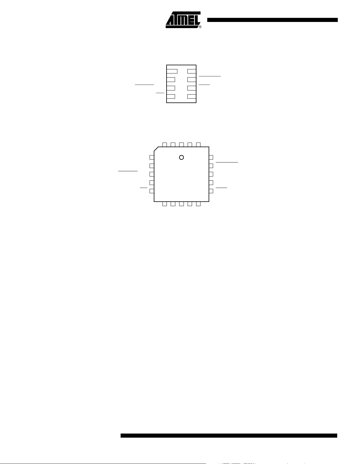
Pin Configuration
8-lead LAP
RESET/OE
CLK
NC
RESET/OE
PAGESEL1
CE
DATA
1
CLK
2
3
CE
4
20-lead PLCC
NC
3
4
5
6
7
8
9
NC
VCC
8
SER_EN
7
CEO (A2)
6
GND
5
DATANCVCC
2
1
20
101112
NC
GND
PAGESEL0
NC
19
18
17
16
15
14
13
NC
NC
SER_EN
PAGE_EN
READY
CEO (A2)
2
AT17F040/080
3039C–CNFG–11/02
Page 3
NC
NC
NC
NC
NC
NC
NC
NC
NC
NC
NC
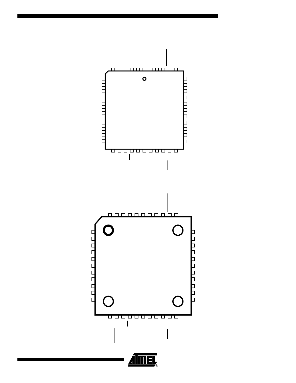
44 PLCC
NC
CLKNCNC
6
5
7
8
9
10
11
12
13
14
15
16
17
1819202122232425262728
DATA
PAGE_EN
VCCNCNC
4
3
2
1
4443424140
SER_EN
NC
39
38
37
36
35
34
33
32
31
30
29
AT17F040/080
NC
NC
NC
NC
NC
NC
NC
NC
NC
NC
READY
NC
NC
NC
NC
NC
NC
NC
NC
NC
NC
NC
1
2
3
4
5
6
7
8
9
10
11
NC
CE
RESET/OE
PAGESEL0
NC
NC
GND
PAGESEL1
NC
NC
CEO/A2
44 TQFP
NC
CLKNCNC
DATA
PAGE_EN
VCCNCNC
SER_EN
NC
4443424140393837363534
33
32
31
30
29
28
27
26
25
24
23
NC
NC
NC
NC
NC
NC
NC
NC
NC
NC
READY
3039C–CNFG–11/02
1213141516171819202122
NC
CE
NC
NC
GND
NC
NC
CEO(A2)
RESET/OE
PAGESEL0
PAGESEL1
3
Page 4
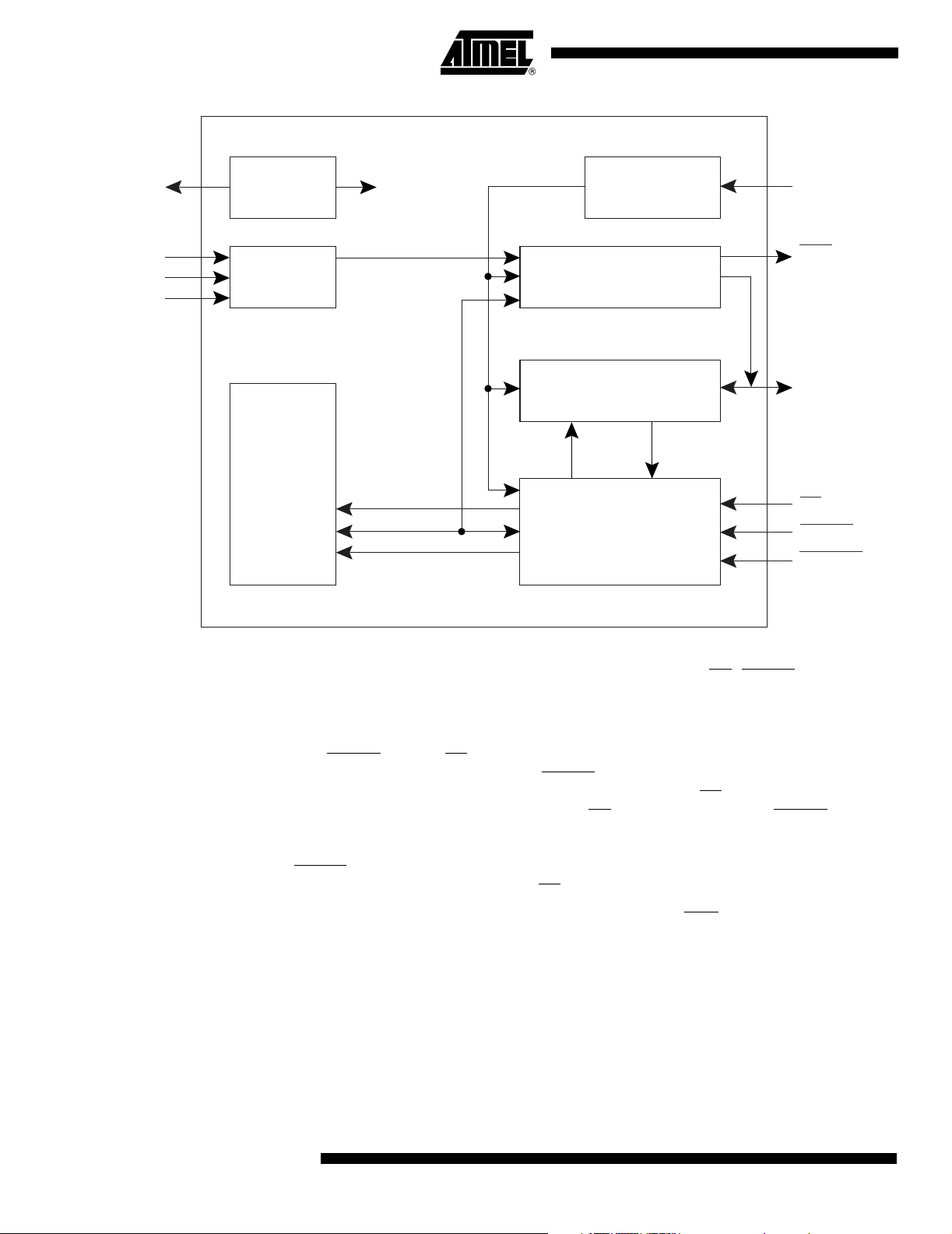
Block Diagram
READY
PAGE_EN
PAGESEL0
PAGESEL1
Power-on
Reset
Config. Page
Select
Flash
Memory
Reset
CE/WE/OE
Data
Address
Clock/Oscillator
Logic
Serial Download Logic
2-wire Serial Programming
Control Logic
CLK
CEO(A2)
DATA
CE
RESET/OE
SER_EN
Device Description
The control signals for the configuration memory device (CE, RESET/OE and CLK)
interface directly with the FPGA device control signals. All FPGA devices can control the
entire configuration process and retrieve data from the configuration device without
requiring an external intelligent controller.
The RESET
enable the address counter. When RESET
resets its address counter and tri-states its DATA pin. The CE
put of the AT17F Series Configurator. If CE
pulse, the counter is disabled and the DATA output pin is tri-stated. When OE is subsequently driven High, the counter and the DATA output pin are enabled. When
RESET
tri-stated, regardless of the state of CE
When the configurator has driven out all of its data and CEO
tri-states the DATA pin to avoid contention with other configurators. Upon power-up, the
address counter is automatically reset.
/OE and CE pins control the tri-state buffer on the DATA output pin and
/OE is driven Low, the configuration device
pin also controls the out-
is held High after the RESET/OE reset
/OE is driven Low again, the address counter is reset and the DATA output pin is
.
is driven Low, the device
4
AT17F040/080
3039C–CNFG–11/02
Page 5
Pin Description
AT17F040/080
AT17F040 AT17F080
8
Name I/O
DATAI/O1212240
CLK I2424543
PAGE_ENI–16–16139
PAGESEL0 I – 11 – 5 20 14
PAGESEL1 I – 7 – 7 25 19
RESET
/OEI36361913
CE
GND – 5 10 5 10 24 18
CEO
A2 I
READY O – 15 – 15 29 23
SER_EN
V
CC
I48482115
O
I7 17 7 174135
–8 20 8 204438
LAP
6 14 6 14 27 21
20
PLCC
8
LAP
20
PLCC
44
PLCC
44
TQFP
DATA Three-state DATA output for configuration. Open-collector bi-directional pin for
programming.
CLK Clock input. Used to increment the internal address and bit counter for reading and
programming.
PAGE _E N Input used to enable page download mode. When PAGE_EN is high the configuration
download address space is partitioned into 4 equal pages. This gives users the ability to
easily store and retrieve multiple configuration bitstreams from a single configuration
device. This input works in conjunction with the PAGESEL inputs. PAGE_EN must be
held low if paging is not desired. When SER_EN is Low (ISP mode) this pin has no
effect.
PAGESEL[1:0] Page select inputs. Used to determine which of the 4 memory pages are targeted during
a serial configuration download. The address space for each of the pages is shown in
Table 2. When SER_EN is Low (ISP mode) these pins have no effect.
Table 2. Address Space
Paging Decodes AT17F040 (4 Mbits) AT17F080 (8 Mbits)
PAGESEL = 00, PAGE_EN = 1 00000 – 0FFFFh 00000 – 1FFFFh
PAGESEL = 01, PAGE_EN = 1 10000 – 1FFFFh 20000 – 3FFFFh
PAGESEL = 10, PAGE_EN = 1 20000 – 2FFFFh 40000 – 5FFFFh
PAGESEL = 11, PAGE_EN = 1 30000 – 3FFFFh 60000 – 7FFFFh
PAGESEL = XX, PAGE_EN = 0 00000 – 3FFFFh 00000 – 7FFFFh
3039C–CNFG–11/02
5
Page 6

RESET/OE Output Enable (active High) and RESET (active Low) when SER_EN is High. A Low
level on RESET
Low) enables the data output driver.
/OE resets both the address and bit counters. A High level (with CE
CE Chip Enable input (active Low). A Low level (with OE High) allows CLK to increment the
address counter and enables the data output driver. A High level on CE
the address and bit counters and forces the device into a low-power standby mode.
Note that this pin will not enable/disable the device in the 2-wire Serial Programming
mode (SER_EN
Low).
disables both
GND Ground pin. A 0.2 µF decoupling capacitor between V
and GND is recommended.
CC
CEO Chip Enable Output (active Low). This output goes Low when the address counter has
reached its maximum value. If the PAGE_EN input is set High, the maximum value is
the highest address in the selected partition. The PAGESEL[1:0] inputs are used to
make the 4 partition selections. If the PAGE_EN input is set Low, the device is not partitioned and the address maxvalue is the highest address in the device, see Table 2 on
page 5. In a daisy chain of AT17F Series devices, the CEO
connected to the CE
is Low and OE is High. It will then follow CE until OE goes Low; thereafter, CEO will stay
High until the entire EEPROM is read again.
input of the next device in the chain. It will stay Low as long as CE
pin of one device must be
A2 Device selection input, A2. This is used to enable (or select) the device during program-
ming (i.e., when SER_EN
is Low). A2 has an internal pull-down resistor.
READY Open collector reset state indicator. Driven Low during power-up reset, released when
power-up is complete. (recommended 4.7 k
W pull-up on this pin if used).
SER_EN Serial enable must be held High during FPGA loading operations. Bringing SER_EN
Low enables the 2-Wire Serial Programming Mode. For non-ISP applications, SER_EN
should be tied to VCC.
V
CC
+3.3V (±10%).
6
AT17F040/080
3039C–CNFG–11/02
Page 7

AT17F040/080
FPGA Master Serial Mode Summary
Control of Configuration
The I/O and logic functions of any SRAM-based FPGA are established by a configuration program. The program is loaded either automatically upon power-up, or on
command, depending on the state of the FPGA mode pins. In Master mode, the FPGA
automatically loads the configuration program from an external memory. The AT17F
Serial Configuration PROM has been designed for compatibility with the Master Serial
mode.
This document discusses the Atmel AT40K, AT40KAL and AT94KAL applications as
well as Xilinx applications.
Most connections between the FPGA device and the AT17F Serial Configurator PROM
are simple and self-explanatory.
• The DATA output of the AT17F Series Configurator drives DIN of the FPGA devices.
• The master FPGA CCLK output drives the CLK input of the AT17F Series
Configurator.
•The CEO
Configurator in a cascade chain of configurator devices.
• SER_EN
• The READY pin is available as an open-collector indicator of the device’s reset
status; it is driven Low while the device is in its power-on reset cycle and released
(tri-stated) when the cycle is complete.
• PAGE_EN must be held Low if download paging is not desired. The PAGESEL[1:0]
inputs must be tied off High or Low. If paging is desired, PAGE_EN must be High
and the PAGESEL pins must be set to High or Low such that the desired page is
selected, see Table 2 on page 5.
output of any AT17F Series Configurator drives the CE input of the next
must be connected to VCC (except during ISP).
Cascading Serial Configuration Devices
For multiple FPGAs configured as a daisy-chain, or for FPGAs requiring larger configuration memories, cascaded configurators provide additional memory.
After the last bit from the first configurator is read, the clock signal to the configurator
asserts its CEO
recognizes the Low level on its CE
After configuration is complete, the address counters of all cascaded configurators are
reset if the RESET
If the address counters are not to be reset upon completion, then the RESET
can be tied to its inactive (High) level.
output Low and disables its DATA line driver. The second configurator
input and enables its DATA output.
/OE on each configurator is driven to its active (Low) level.
/OE input
Programming Mode The programming mode is entered by bringing SER_EN Low. In this mode the chip can
be programmed by the 2-wire serial bus. The programming is done at V
Programming super voltages are generated inside the chip. The AT17F parts are
read/write at 3.3V nominal. Refer to the AT17F Configuration application note available
on the Atmel web site (www.atmel.com) for more programming details.
supply only.
CC
Standby Mode The AT17F Series Configurators enter a low-power standby mode whenever CE is
asserted High. In this mode, the AT17F Configurator consumes less than 50 µA of current at 3.3V. The output remains in a high-impedance state regardless of the state of the
input.
OE
3039C–CNFG–11/02
7
Page 8

Absolute Maximum Ratings*
Operating Temperature...................................... -4°C to +85°C
Storage Temperature..................................... -65 °C to +150°C
Voltage on Any Pin
with Respect to Ground..............................-0.1V to V
Supply Voltage (V
) .........................................-0.5V to +4.0V
CC
Maximum Soldering Temp. (10 sec. @ 1/16 in.).............260°C
+0.5V
CC
*NOTICE: Stresses beyond those listed under Absolute
Maximum Ratings may cause permanent damage to the device. This is a stress rating only and
functional operation of the device at these or any
other conditions beyond those listed under operating conditions is not implied. Exposure to Absolute Maximum Rating conditions for extended
periods of time may affect device reliability.
ESD (R
= 1.5K, C
ZAP
= 100 pF)................................. 2000V
ZAP
Operating Conditions
Symbol Description
Commercial
V
CC
Industrial
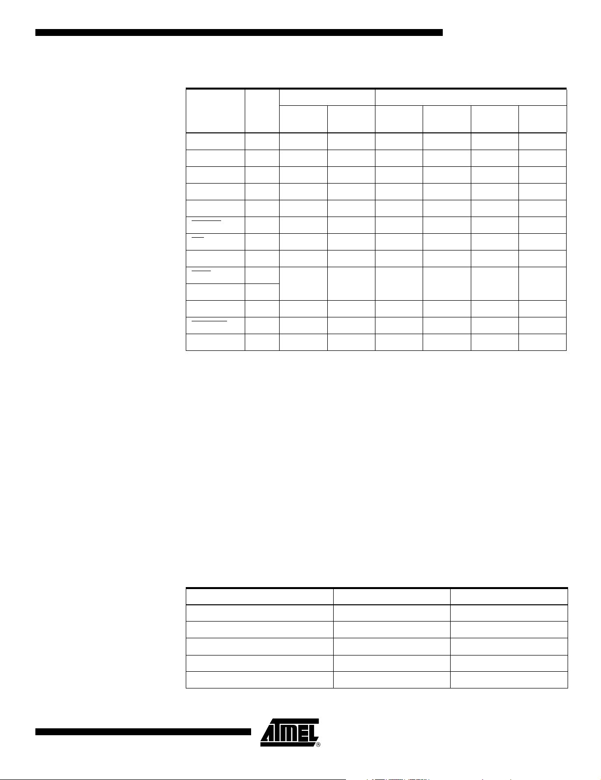
DC Characteristics
Symbol Description
V
V
V
V
V
V
I
CCA
I
L
I
CCS
IH
IL
OH
OL
OH
OL
High-level Input Voltage 2.0 V
Low-level Input Voltage 0 0.8 0 0.8 V
High-level Output Voltage (IOH = -2.5 mA)
Low-level Output Voltage (IOL = +3 mA) 0.4 0.4 V
High-level Output Voltage (IOH = -2 mA)
Low-level Output Voltage (IOL = +3 mA) 0.4 0.4 V
Supply Current, Active Mode 5 5 mA
Input or Output Leakage Current (VIN = VCC or GND) -10 10 -10 10 µA
Supply Current, Standby Mode
Supply voltage relative to GND
-0°C to +70°C
Supply voltage relative to GND
-40°C to +85°C
Commercial
Industrial
Commercial 100 200 µA
Industrial 100 200 µA
AT17F Series Configurator
UnitsMin Max
2.97 3.63 V
2.97 3.63 V
AT17F040 AT17F080
UnitsMinMaxMinMax
CC
2.0 V
CC
2.4 2.4 V
2.4 2.4 V
V
8
AT17F040/080
3039C–CNFG–11/02
Page 9

AC Characteristics
CE
RESET/OE
CLK
T
SCE
AT17F040/080
T
SCE
T
T
LC
T
HC
HOE
T
HCE
T
OE
T
CE
DATA
AC Characteristics when Cascading
RESET/OE
CE
CLK
T
CDF
DATA
CEO
LAST BIT
T
OCK
T
CAC
T
OCE
T
OH
T
OOE
T
DF
T
OH
FIRST BIT
3039C–CNFG–11/02
T
OCE
9
Page 10
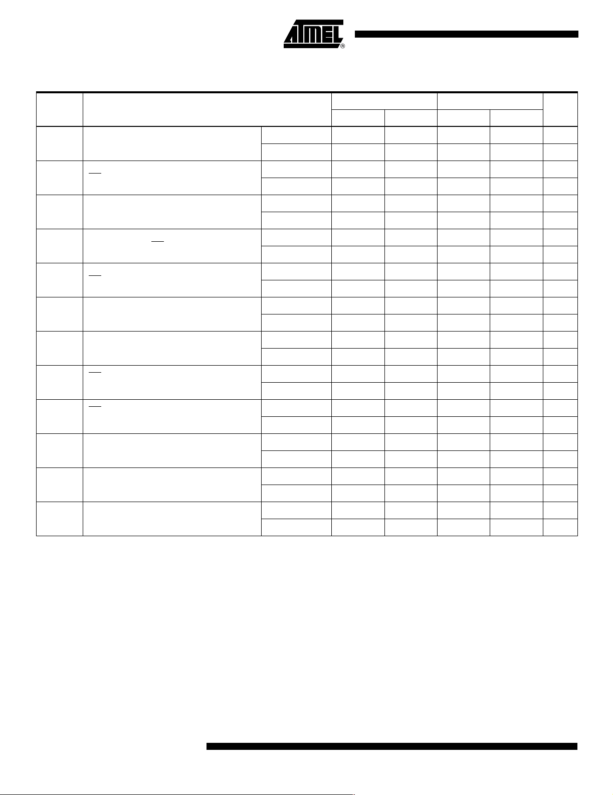
AC Characteristics
Symbol Description
AT17F040 AT17F080
UnitsMin Max Min Max
(1)
T
OE
(1)
T
CE
T
CAC
OE to Data Delay
CE to Data Delay
(1)
CLK to Data Delay
Commercial 50 50 ns
Industrial 55 55 ns
Commercial 60 55 ns
Industrial 60 60 ns
Commercial 75 55 ns
Industrial 80 60 ns
Commercial 0 0 ns
T
OH
(2)
T
DF
Data Hold from CE, OE, or CLK
Industrial 0 0 ns
Commercial 55 50 ns
CE or OE to Data Float Delay
Industrial 55 50 ns
Commercial 20 20 ns
T
LC
CLK Low Time
Industrial 20 20 ns
Commercial 20 20 ns
T
HC
T
SCE
T
HCE
CLK High Time
CE Setup Time to CLK
(to guarantee proper counting)
CE Hold Time from CLK
(to guarantee proper counting)
Industrial 20 20 ns
Commercial 35 20 ns
Industrial 40 25 ns
Commercial 0 0 ns
Industrial 0 0 ns
T
F
F
HOE
MAX
MAX
OE High Time
(guarantees counter is reset)
Maximum Input Clock Frequency
SEREN = 0
Maximum Input Clock Frequency
SEREN = 1
Notes: 1. AC test lead = 50 pF.
2. Float delays are measured with 5 pF AC loads. Transition is measured ± 200 mV from steady-state active levels.
Commercial 20 20 ns
Industrial 20 20 ns
Commercial 10 10 MHz
Industrial 10 10 MHz
Commercial 33 33 MHz
Industrial 33 33 MHz
10
AT17F040/080
3039C–CNFG–11/02
Page 11

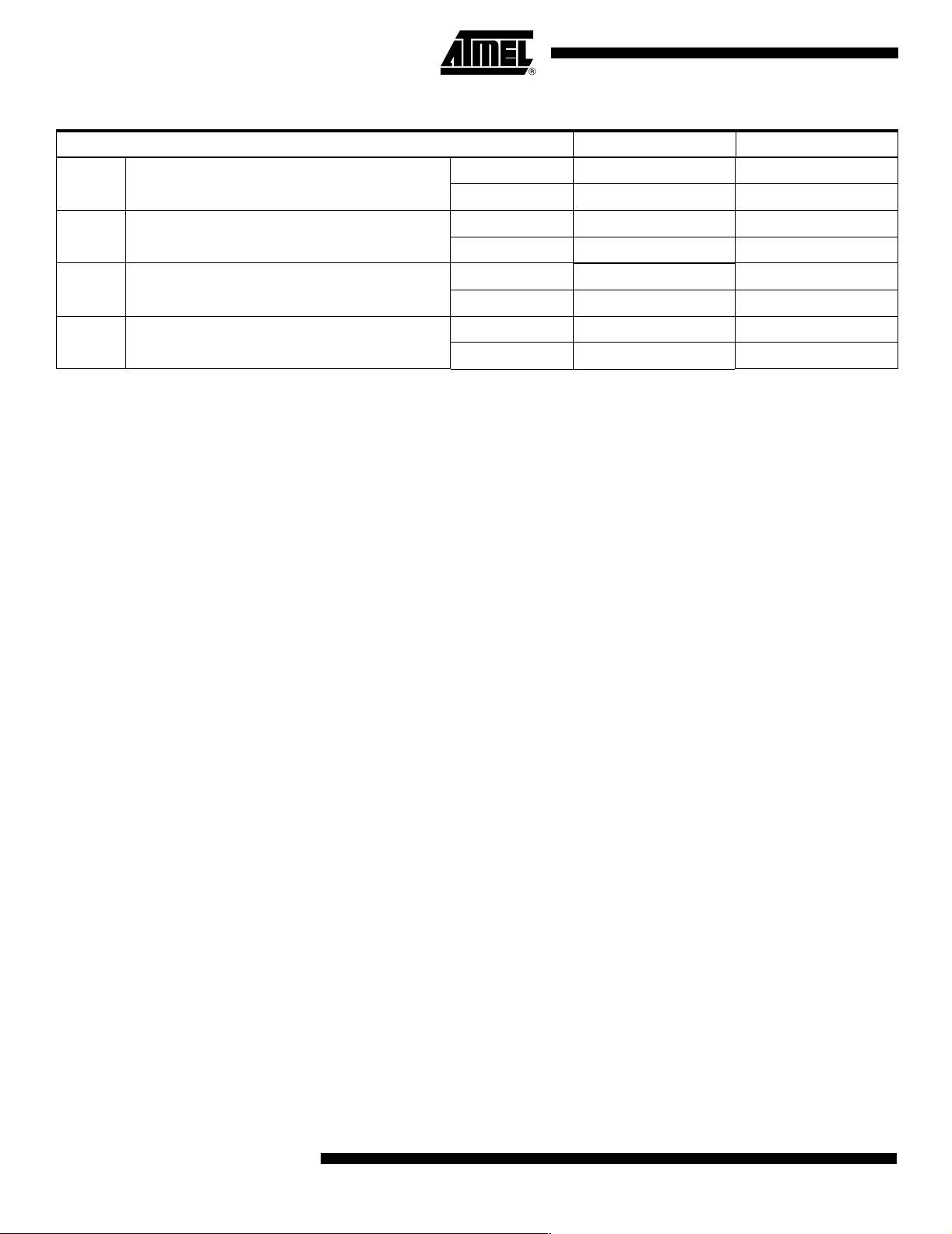
AC Characteristics When Cascading
AT17F040/080
AT17F040 AT17F080
Symbol Description
T
T
T
T
F
CDF
OCK
OCE
OOE
MAX
(2)
(1)
(1)
(1)
CLK to Data Float Delay
CLK to CEO Delay
CE to CEO Delay
RESET/OE to CEO Delay
Maximum Input Clock Frequency
Notes: 1. AC test lead = 50 pF.
2. Float delays are measured with 5 pF AC loads. Transition is measured ± 200 mV from steady-state active levels.
UnitsMin Max Min Max
Commercial 60 50 ns
Industrial 60 50 ns
Commercial 55 50 ns
Industrial 60 55 ns
Commercial 55 35 ns
Industrial 60 40 ns
Commercial 40 35 ns
Industrial 45 35 ns
Commercial 33 33 MHz
Industrial 33 33 MHz
3039C–CNFG–11/02
11
Page 12
Thermal Resistance Coefficients
(1)
Package Type AT17F040 AT17F080
[°C/W] –
q
8CN4 Leadless Array Package (LAP)
20J Plastic Leaded Chip Carrier (PLCC)
44A Thin Plastic Quad Flat Package (TQFP)
44J Plastic Leaded Chip Carrier (PLCC)
JC
qJA [°C/W]
q
JC
q
JA
q
JC
q
JA
q
JC
qJA [°C/W]
(2)
[°C/W] –
(2)
[°C/W]
[°C/W] – 17
(2)
[°C/W]
–62
[°C/W] – 15
(2)
–50
–
–
Notes: 1. For more information refer to the “Thermal Characteristics of Atmel’s Packages”, available on the Atmel web site, at
http://www.atmel.com/atmel/acrobat/doc0636.pdf.
2. Airflow = 0 ft/min.
12
AT17F040/080
3039C–CNFG–11/02
Page 13

AT17F040/080
Ordering Information
Memory Size Ordering Code Package Operation Range
4-Mbit AT17F040-30CC
AT17F040-30BJC
AT17F040-30CI
AT17F040-30BJI
8-Mbit AT17F080-30CC
AT17F080-30JC
AT17F080-30TQC
AT17F080-30BJC
AT17F080-30CI
AT17F080-30JI
AT17F080-30TQI
AT17F080-30BJI
8CN4 - 8 LAP
20J - 20 PLCC
8CN4 - 8 LAP
20J - 20 PLCC
8CN4 - 8 LAP
20J - 20 PLCC
44A - 44 TQFP
44J - 44 PLCC
8CN4 - 8 LAP
20J - 20 PLCC
44A - 44 TQFP
44J - 44 PLCC
(0°C to 70°C)
(-40°C to 85°C)
(0°C to 70°C)
(-40°C to 85°C)
Commercial
Industrial
Commercial
Industrial
Package Type
8CN4 8-lead, 6 mm x 6 mm x 1 mm, Leadless Array Package (LAP) – Pin-compatible with 8-lead SOIC/VOID Packages
20J 20-lead, Plastic J-leaded Chip Carrier (PLCC)
44A 44-lead, Thin (1.0 mm) Plastic Quad Flat Package Carrier (TQFP)
44J 44-lead, Plastic J-leaded Chip Carrier (PLCC)
3039C–CNFG–11/02
13
Page 14

Packaging Information
8CN4 – LAP
Marked Pin1 Indentifier
E
D
A
A1
Top View
0.10 mm
TYP
8
e
7
6
5
e1
Bottom View
Note: 1. Metal Pad Dimensions.
L1
Side View
Pin1 Corner
1
COMMON DIMENSIONS
2
SYMBOL
3
b
4
L
A 0.94 1.04 1.14
A1 0.30 0.34 0.38
b 0.45 0.50 0.55 1
D 5.89 5.99 6.09
E 4.89 5.99 6.09
e 1.27 BSC
e1 1.10 REF
L 0.95 1.00 1.05 1
L1 1.25 1.30 1.35 1
(Unit of Measure = mm)
MIN
NOM
MAX
NOTE
14
2325 Orchard Parkway
R
San Jose, CA 95131
AT17F040/080
TITLE
8CN4, 8-lead (6 x 6 x 1.04 mm Body), Lead Pitch 1.27 mm,
Leadless Array Package (LAP)
DRAWING NO.
8CN4
3039C–CNFG–11/02
11/14/01
REV.
A
Page 15

20J – PLCC
AT17F040/080
1.14(0.045) X 45˚
B
0.51(0.020)MAX
45˚ MAX (3X)
Notes: 1. This package conforms to JEDEC reference MS-018, Variation AA.
2. Dimensions D1 and E1 do not include mold protrusion.
Allowable protrusion is .010"(0.254 mm) per side. Dimension D1
and E1 include mold mismatch and are measured at the extreme
material condition at the upper or lower parting line.
3. Lead coplanarity is 0.004" (0.102 mm) maximum.
PIN NO. 1
IDENTIFIER
e
E1 E
D1
D
1.14(0.045) X 45˚
0.318(0.0125)
0.191(0.0075)
D2/E2
B1
A2
A1
A
COMMON DIMENSIONS
(Unit of Measure = mm)
SYMBOL
A 4.191 – 4.572
A1 2.286 – 3.048
A2 0.508 – –
D 9.779 – 10.033
D1 8.890 – 9.042 Note 2
E 9.779 – 10.033
E1 8.890 – 9.042 Note 2
D2/E2 7.366 – 8.382
B 0.660 – 0.813
B1 0.330 – 0.533
e 1.270 TYP
MIN
NOM
MAX
NOTE
2325 Orchard Parkway
R
San Jose, CA 95131
3039C–CNFG–11/02
TITLE
20J, 20-lead, Plastic J-leaded Chip Carrier (PLCC)
DRAWING NO.
20J
10/04/01
REV.
B
15
Page 16

44A – TQFP
PIN 1
B
PIN 1 IDENTIFIER
e
E1 E
D1
D
C
0˚~7˚
A1
L
Notes: 1. This package conforms to JEDEC reference MS-026, Variation ACB.
2. Dimensions D1 and E1 do not include mold protrusion. Allowable
protrusion is 0.25 mm per side. Dimensions D1 and E1 are maximum
plastic body size dimensions including mold mismatch.
3. Lead coplanarity is 0.10 mm maximum.
A2 A
SYMBOL
COMMON DIMENSIONS
(Unit of Measure = mm)
MIN
A – – 1.20
A1 0.05 – 0.15
A2 0.95 1.00 1.05
D 11.75 12.00 12.25
D1 9.90 10.00 10.10 Note 2
E 11.75 12.00 12.25
E1 9.90 10.00 10.10 Note 2
B 0.30 – 0.45
C 0.09 – 0.20
L 0.45 – 0.75
e 0.80 TYP
NOM
MAX
NOTE
16
2325 Orchard Parkway
TITLE
R
San Jose, CA 95131
AT17F040/080
44A, 44-lead, 10 x 10 mm Body Size, 1.0 mm Body Thickness,
0.8 mm Lead Pitch, Thin Profile Plastic Quad Flat Package (TQFP)
10/5/2001
DRAWING NO.
44A
3039C–CNFG–11/02
REV.
B
Page 17

44J – PLCC
AT17F040/080
1.14(0.045) X 45˚
B
e
0.51(0.020)MAX
45˚ MAX (3X)
Notes: 1. This package conforms to JEDEC reference MS-018, Variation AC.
2. Dimensions D1 and E1 do not include mold protrusion.
Allowable protrusion is .010"(0.254 mm) per side. Dimension D1
and E1 include mold mismatch and are measured at the extreme
material condition at the upper or lower parting line.
3. Lead coplanarity is 0.004" (0.102 mm) maximum.
PIN NO. 1
IDENTIFIER
D1
D
1.14(0.045) X 45˚
E1 E
0.318(0.0125)
0.191(0.0075)
NOM
D2/E2
MAX
B1
A2
A1
A
COMMON DIMENSIONS
(Unit of Measure = mm)
SYMBOL
A 4.191 – 4.572
A1 2.286 – 3.048
A2 0.508 – –
D 17.399 – 17.653
D1 16.510 – 16.662 Note 2
E 17.399 – 17.653
E1 16.510 – 16.662 Note 2
D2/E2 14.986 – 16.002
B 0.660 – 0.813
B1 0.330 – 0.533
e 1.270 TYP
MIN
NOTE
2325 Orchard Parkway
R
San Jose, CA 95131
3039C–CNFG–11/02
TITLE
44J, 44-lead, Plastic J-leaded Chip Carrier (PLCC)
DRAWING NO.
44J
10/04/01
REV.
B
17
Page 18

Atmel Headquarters Atmel Operations
Corporate Headquarters
2325 Orchard Parkway
San Jose, CA 95131
TEL 1(408) 441-0311
FAX 1(408) 487-2600
Europe
Atmel Sarl
Route des Arsenaux 41
Case Postale 80
CH-1705 Fribourg
Switzerland
TEL (41) 26-426-5555
FAX (41) 26-426-5500
Asia
Room 1219
Chinachem Golden Plaza
77 Mody Road Tsimhatsui
East Kowloon
Hong Kong
TEL (852) 2721-9778
FAX (852) 2722-1369
Japan
9F, Tonetsu Shinkawa Bldg.
1-24-8 Shinkawa
Chuo-ku, Tokyo 104-0033
Japan
TEL (81) 3-3523-3551
FAX (81) 3-3523-7581
Memory
2325 Orchard Parkway
San Jose, CA 95131
TEL 1(408) 441-0311
FAX 1(408) 436-4314
Microcontrollers
2325 Orchard Parkway
San Jose, CA 95131
TEL 1(408) 441-0311
FAX 1(408) 436-4314
La Chantrerie
BP 70602
44306 Nantes Cedex 3, France
TEL (33) 2-40-18-18-18
FAX (33) 2-40-18-19-60
ASIC/ASSP/Smart Cards
Zone Industrielle
13106 Rousset Cedex, France
TEL (33) 4-42-53-60-00
FAX (33) 4-42-53-60-01
1150 East Cheyenne Mtn. Blvd.
Colorado Springs, CO 80906
TEL 1(719) 576-3300
FAX 1(719) 540-1759
Scottish Enterprise Technology Park
Maxwell Building
East Kilbride G75 0QR, Scotland
TEL (44) 1355-803-000
FAX (44) 1355-242-743
RF/Automotive
Theresienstrasse 2
Postfach 3535
74025 Heilbronn, Germany
TEL (49) 71-31-67-0
FAX (49) 71-31-67-2340
1150 East Cheyenne Mtn. Blvd.
Colorado Springs, CO 80906
TEL 1(719) 576-3300
FAX 1(719) 540-1759
Biometrics/Imaging/Hi-Rel MPU/
High Speed Converters/RF Datacom
Avenue de Rochepleine
BP 123
38521 Saint-Egreve Cedex, France
TEL (33) 4-76-58-30-00
FAX (33) 4-76-58-34-80
Atmel Programmable SLI Hotline
(408) 436-4119
Atmel Programmable SLI e-mail
configurator@atmel.com
e-mail
literature@atmel.com
Web Site
http://www.atmel.com
FAQ
Available on web site
© Atmel Corporation 2002.
Atmel Corporation makes no warranty for the use of its products, other than those expressly contained in the Company’s standard warranty
which is detailed in Atmel’s Terms and Conditions located on the Company’s web site. The Company assumes no responsibility for any errors
which may appear in this document, reserves the right to change devices or specifications detailed herein at any time without notice, and does
not make any commitment to update the information contained herein. No licenses to patents or other intellectual property of Atmel are granted
by the Company in connection with the sale of Atmel products, expressly or by implication. Atmel’s products are not authorized for use as critical
components in life support devices or systems.
Atmel® is the registered trademark of Atmel.
™
is the trademark of Altera Corporation; ORCA™ is the trademark of Lucent Technologies, Inc.;
FLEX
SPARTAN
the trademarks of Xilinx, Inc.; APEX
may be the trademarks of others.
®
and Virtex® are the registered trademarks of Xilinx, Inc.; XC3000™, XC4000™ and XC5200™ are
™
is the trademark of MIPS Technologies; Other terms and product names
Printed on recycled paper.
3039C–CNFG–11/02
xM
 Loading...