

Page 1

INTEGRATED CIRCUITS INC.- APR9301
APR9301 RE-RECORDING VOICE IC
Single-Chip Voice Recording & Playback Device
for Single 20 to 30 Second Message
Features :
Single-chip, high quality voice recording & Playback solution
- No external ICs required
- Minimum external components
Non-volatile Flash memory technology
- No battery backup required
- 100K record cycles (typical)
- 100-year message retention (typical)
Single message of 20 to 30 seconds, with external resistor selection
Chip enable pin for simple message expansion
User-friendly, easy-to-use operation
- Programming & development systems not required
- Level-activated recording & edge-activated playback switches
Low power consumption
- Operating current: 25mA (typical, no load)
- Standby current: 1uA (typical, no load)
Automatic power-down feature for longer battery life
Single 5V power supply
General Description :
The APR9301 device offers true single-chip solid-state storage capability and requires no
software or microcont-roller support. It provides high-quality recording and playback with a
single 20- to 30-second message. It is ideal for portable voice recorders, toys, and many
other consumer and industrial applications.
APLUS’s proprietary analog/multi-level storage technology is implemented in advanced
Flash non-volatile memory cells,each of which can typically store more than 256 voltage
levels. The APR9301 device stores and reproduces voice signals in their natural forms,
eliminating distortion that is often introduced by encoding and compression. The device
combines a small size with low power consumption,non-volatility, and ease-of-use for a cost
effective solution to voice recording and playback
http://www.aplusinc.com.tw Page / 10 VER2.1
1
Page 2
INTEGRATED CIRCUITS INC.- APR9301
PS : The APR9301 DIP & SOP is not [ PIN to PIN ]
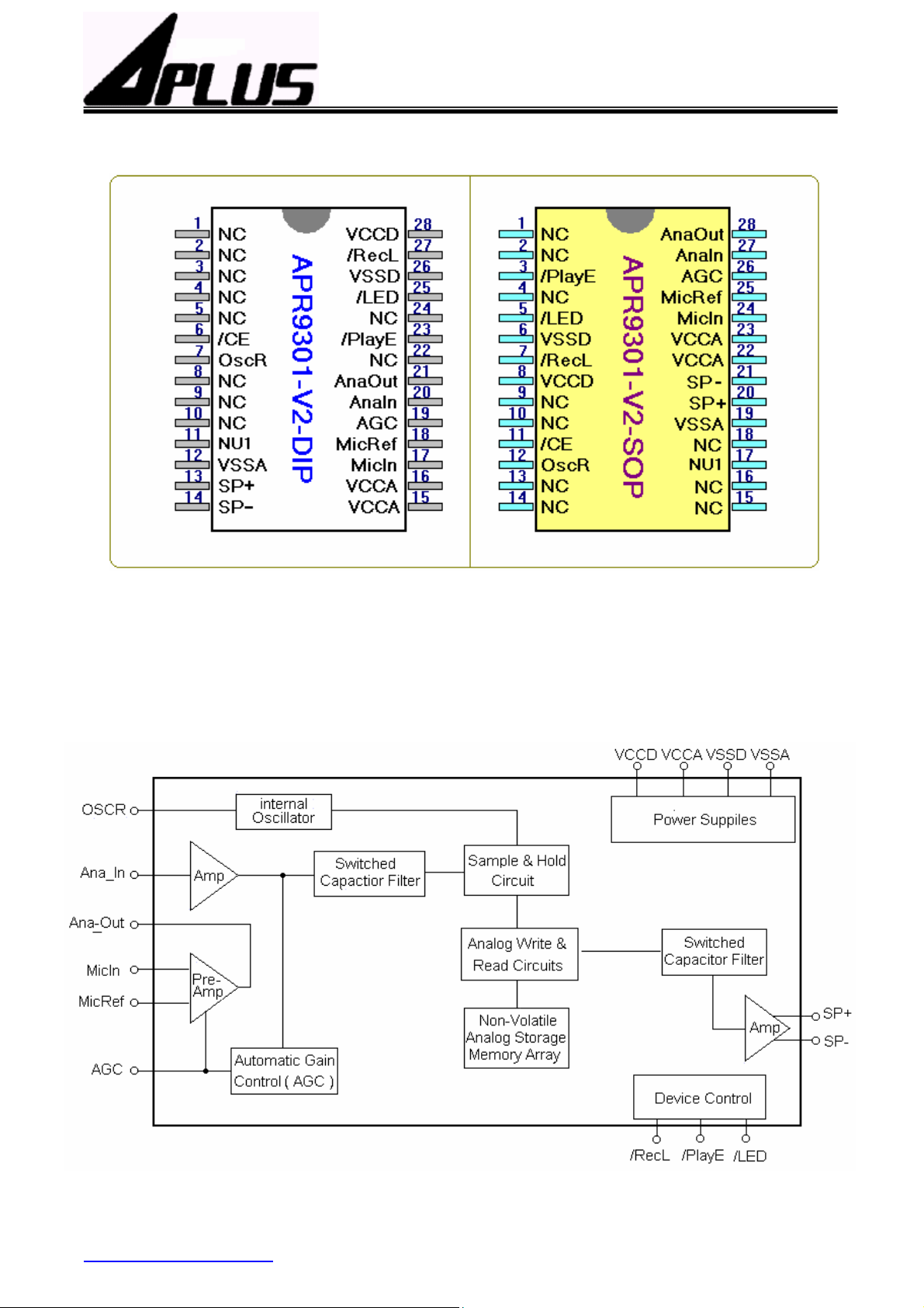
Functional Block Diagram :
Figure 2 shows the functional block diagram for the APR9301 device.
Figure 2 APR9301 Functional Block Diagram
http://www.aplusinc.com.tw Page / 10 VER2.1
2
Page 3

A
INTEGRATED CIRCUITS INC.- APR9301
Sample Application
Figure 3 shows the diagram for a single,
20-second message recording and
playback application using the APR9301
device. When pins are connected as shown
in this example,the operating modes are as
follows:
Record Mode (Level-Activated)
single voice message of up to 20 seconds
can be recorded.The /LED pin will go low
during the actual recording process to
provide a visual indication if an LED light is
connected to this pin. The chip is in record
Playback Mode (Edge-Activated)
Playback always starts from the beginning
of the message.The chip is in playback
mode after the /PlayE pin pulses low
(edge-activated). Playback will stop
immediately when the /PlayE pin pulses low
a second time.
If the newly recorded message is shorter
than the previously recorded message,
the remaining portion of the previous
message will not be played after the new
message is played back.
The input preamplifier, AGC, and main
amplifier circuits are disabled during
mode as long as the /RecL pin stays low
level-activated). If the message lasts longer
than 20 seconds, recording will terminate
automatically after the last available
memory cell is written. If the message is
shorter
than 20 seconds, the recording operation
will stop when the /RecL pin goes high.
The speaker driver is automatically
tristated during the recording operation.
Messages of up to 30 seconds can be
recorded by using
different OscR resistor values
(see Table 1).
playback.
Standby Mode (/CE = "0)
The chip will automatically return to the
standby state after recording or playback
operation is completed.
Power Down Mode (/CE = "1 `)
The chip is always in standby state.
No recording or playback is allowed.
Current consumption is typically less than
1uA.
http://www.aplusinc.com.tw Page / 10 VER2.1
3
Page 4

INTEGRATED CIRCUITS INC.- APR9301
Figure 3 Sample Application for the APR9301 :
NC=No Connect (must be floating)
Pins 23 and 27 have internal pull-up resistors.
The typical sampling frequency is 6.4kHz with OscR=52Kω
Table 1 Typical Dependence of Sampling Frequency and Total Voice Duration on OscR
Resistor Value
(VccA = VccD = 5V; VssA = Vssd = 0V; TA = 25℃)
Cutoff
Frequency
(3dB Point)
Total Voice Duration
Working Voltage
Typical
OscR value
38KΩ
52KΩ
67KΩ
75KΩ
Sampling Frequency
Typical
8KHZ 3.4KHZ 16 SECONDS 4.5V ~ 6.5V
KHZ 2.7KHZ 20 SECONDS 4.5V ~ 6.5V
6.4
5.3KHZ 2.3KHZ 24 SECONDS 4.8V ~ 6.5V
4.5KHZ 2KHZ 30 SECONDS 5.2V ~ 6.5V
http://www.aplusinc.com.tw Page / 10 VER2.1
4
Page 5

INTEGRATED CIRCUITS INC.- APR9301
Figure 4 shows the same application using external microphone biasing instead of the
microphone amplifier on the APR9301 device, thus bypassing the preamplifier portion
of the chip function.
Figure 4 Sample Application Using External Microphone Biasing :
Notes:
NC=No Connect (must be floating).
Pins 23 and 27 have internal pull-up resistors.
The typical sampling frequency is 6.4kHz with OscR=52kΩ
NPN bipolar transistor,T1 model #MPS3904 or equivalent.
Electrical Characteristics
Tables 2 through 4 list Absolute Maximum Ratings, Recommended DC Characteristics,
and recommended Analog Characteristics for the APR9301 device
http://www.aplusinc.com.tw Page / 10 VER2.1
5
Page 6

INTEGRATED CIRCUITS INC.- APR9301
Absolute Maximum Ratings
Stresses greater than those listed in Table 2 may cause permanent damage to the
device. These specifications represent a stress rating only. Operation of the device at
these or any other conditions above those specified in the recommended DC
Characteristics or recommended Analog Characteristics of this specification is not
implied. Operation of the device at maximum conditions for extended periods may affect
reliability.
Table 2 Absolute Maximum Ratings.
Item Symbol Condition Min Max Unit
Power Supply Voltage Vcc
Input Voltage VIN1
Input Voltage VIN2
Storage Temperature TSTG -- -65 150
Temperature Under Bias TBS -- -65 125
Lead Temperature TLD <10s -- 300
TA = 25℃
TA = 25℃
︱IIN︱ <20 mA
4.5 6.5 V
-0.3 Vcc +0.3 V
-1.0 Vcc +1.0 V
Table 3 DC Characteristics ( Note 1 )
Item Symbol Condition Mm Typ Max Unit
Input High Voltage VIH -- 0.8 x Vcc -- -- V
Input Low Voltage VIL -- -- -- 0.8 V
Output High Voltage VOH IOL = -1 .6mA 2.4 -- -- V
Output Low Voltage VOL IOL = 4.0mA -- -- 0.45 V
℃
℃
℃
Input Leakage Current IIH VIH = Vcc -- -- 1.0 uA
Input Leakage Current IIL VIL = Vss(Note 2) -1.0 -- -- uA
Output Tristate Leakage Current Ioz
Operating Current Consumption Icc Internal Clock, No Load -- 25 -- mA
Standby Current Consumption lccs No Load -- 1.0 -- uA
http://www.aplusinc.com.tw Page / 10 VER2.1
VOUT = VCC or VOUT=VSS
6
-1.0 -- 1.0 uA
Page 7

INTEGRATED CIRCUITS INC.- APR9301
Table 4 Analog Characteristics ( Note 1 )
Item Symbol Condition Mim Typ Max Unit
MicIn Input Voltage VMI -- -- -- 20 mVp-p
MicIn Input Resistance RMI -- -- 10 --
MicIn Amp Gain (1) GMIl
MicIn Amp Gain (2) GMI2
AnaIn Input Voltage VANI -- -- -- 50 mVp-p
AnaIn Input Resistance RANI -- -- 10 --
AnaIn Amp Gain GANI Analn to SP+/- -- 22 -- dB
AGC Output Resistance RAGC -- -- 1 --
SP+/- Output Power Psp
Voltage Amplitude Across SP+/- Vsp
Total Harmonic Distortion THD
AGC≦2.2V
AGC≧3.OV
Rsp+/- = 16Ω
Rsp+/-≧16Ω
@ 1kHz & 20mVp-p input
-- 24 -- dB
-- -45 -15 dB
-- 12.2 -- mW
-- 1.25 -- Vp-p
1 %
Note 1: Typical Values: VCCD = VCCA = 5V; VSSD = VSSA = 0V; TA = 25℃
Note 2: Except pins 23 and 27 which have internal pull-up resistors.
Bonding Pad Diagram & Description of Bonding Pad Coordinates :
Figure 5 APR9301 Die Bonding Pad Diagram
Notes:
Die diagram is with
respect to die center(um)
Die Dimensions:
X=214± 1 mils(5500um)
Y=144± 1 mils(3750um)
Die Thickness:
13.8± 1.0 mils
(350± 25um)
Pad Opening:
4.3mils
110um
* Connect substrate
to Ground.
kΩ
kΩ
kΩ
http://www.aplusinc.com.tw Page / 10 VER2.1
7
Page 8

INTEGRATED CIRCUITS INC.- APR9301
Table 5 APR9301 Bonding Pad Coordinates :
Pin Pin Name X – Axis (Note) Y – Axis (Note)
/CE Chip Enable -2496.2 1565.8
OscR
NU1 Connect to Ground -1808.45 -1496.1
VSSD Digital Ground Supply -1564.05 -1572
VSSA Analog Ground Supply -1384.05 -1548.7
VSSA Analog Ground Supply -1204.35 -1477.1
SP+ Non-Inverting Speaker Output -707.15 -1390
SP- Inverting Speaker Output 479.15 -1389.9
VCCA Analog Power Supply 976.45 -1492
VCCA Analog Power Supply 1190.4 -1523.7
MinIn Microphone Input 1619.45 -1551.4
MicRef Microphone Reference Input 2035.45 -1551.4
Oscillator Frequency-Setting
Resistor
-2459.55 729.8
AGC Automatic Gain Control 2487.45 -1551.4
AnaIn Analog Signal Input 2487.45 -1049.9
AnaOut Analog Signal Output 2487.45 -648.9
/PlayE Edge-Activated Playback 2493.65 1371.1
/LED LED Output 1430.7 1565.8
VSSD Connect to Ground 865.75 1565.8
/RecL Level-Activated Record 258.15 1565.8
VCCD Digital Power Supply -229.4 1579.05
VCCD Digital Power Supply -510.8 1541.6
Note: With respect to die center(um)
http://www.aplusinc.com.tw Page / 10 VER2.1
8
Page 9

INTEGRATED CIRCUITS INC.- APR9301
PACKAGE OUTLINE : SOP – 28 ( 330 MIL )
http://www.aplusinc.com.tw Page / 10 VER2.1
9
Page 10

INTEGRATED CIRCUITS INC.- APR9301
PACKAGE OUTLINE : DIP – 28 ( 600 MIL )
http://www.aplusinc.com.tw Page / 10 VER2.1
10
 Loading...