

Page 1
PLUS MAKE YOUR PRODUCTION A-PLUS
A
APExx24 Series
DATA SHEET
PLUS INTEGRATED CIRCUITS INC.
A
Address:
3 F-10, No. 32, Sec. 1, Chenggung Rd., Taipei,
Taiwan 115, R.O.C.
(115)台北市南港區成功路㆒段 32 號 3 樓之 10.
TEL: 886-2-2782-9266
FAX: 886-2-2782-9255
WEBSITE : http: //www.aplusinc.com.tw
Sales E-mail:
sales@aplusinc.com.tw
Technology E-mail:
service@aplusinc.com.tw
Page 2
APExx24 Series
1.0 General Description
The APExx24 series are very low cost voice and melody synthesizer with 4-bits CPU. They have various
features including 4-bits ALU, ROM, RAM, I/O ports, timers, clock generator, voice and melody
synthesizer, and PWM (Direct drive) or D/A current outputs, etc. The audio synthesizer contains one
voice-channel and two melody-channels. Furthermore, they consist of 27 instructions in these devices.
With CMOS technology and halt function can minimize power dissipation. Their architectures are similar
to RISC, with two stages of instruction pipeline. They allow all instructions to be executed in a single
cycle, except for program branches and data table read instructions (which need two instruction cycles).
2.0 Features
(1) Single power supply can operate from 2.4V to 5.5V at 4MHz or 8MHz.
(2) Program ROM: 64k x 10 bits
(3) 1 set of 16-bits DPR can access up to 64k x 10 bits melody data memory space, and 1 set of 20-bits
VPR can access up to 1024k x 10 bits voice data memory space.
Product Voice Duration (sec) Voice Pointer (VPR) ROM Size (10-bits)
APE12724 127 19-bits 384k
APE17024 170 19-bits 512k
APE25524 255 20-bits 768k
APE34024 340 20-bits 1024k
(4) Data Registers:
a). 128 x 4-bits data RAM (00-7Fh)
b). Unbanked special function registers (SFR) range: 00h-2Fh
(5) I/O Ports:
a). PRA: 4-bits I/O Port A (10h) can be programmed to input/output individually. (Regist er control)
b). PRB: 4-bits I/O Port B (13h) can be configured to input/output individually. (Mask option)
c). PR C: 4-bits I/O Port C (14h) can be programmed to input/output individually. (Register control)
d). PRD: 4-bits I/O Port D (15h) can be programmed to input/output individually. (Register control)
e). PRE: 4-bits I/O Port E (17h) can be programmed to input/ out put individually. (Register control)
f). PRF: 4-bits I/O Port F (18h) can be programmed to input/output individually. (Register control)
(6) On-chip clock generator: Resistive Clock Drive (RM) or Crystal oscillator (HM)
(7) Timer: 1-set Voice Interrupt (Timer0: a 9-bits auto-reload timer/counter).
(8) Stack: 2-level subroutine nesting.
(9) B uilt-in 4 Level Vol u me C ontrol can be prog r amm ed .
(10) Built-in 8 Level DAC Current Control can be configured. (Mask option)
(11) Built-in IR Carry Output: Port B[1] can be configured as IR pin by 38k / 56kHz. (Mask option)
1
Rev 1.5 2004/4/20
Page 3
APExx24 Series
(12) External Reset: Port B[3] can be configured as reset pin. (Mask opt on)
(13) HALT and Release from HALT function to reduce power consumpt ion
(14) Watch Dog Timer (WDT)
(15) Instruction: 1-cycle instruction except for table read and program branches which are 2-cycles
(16) Number of instruction: 27
(17) DAC: 1 channel voice and dual tone melody synthesizer (One 9-bits Cout or 8-bits PWM output).
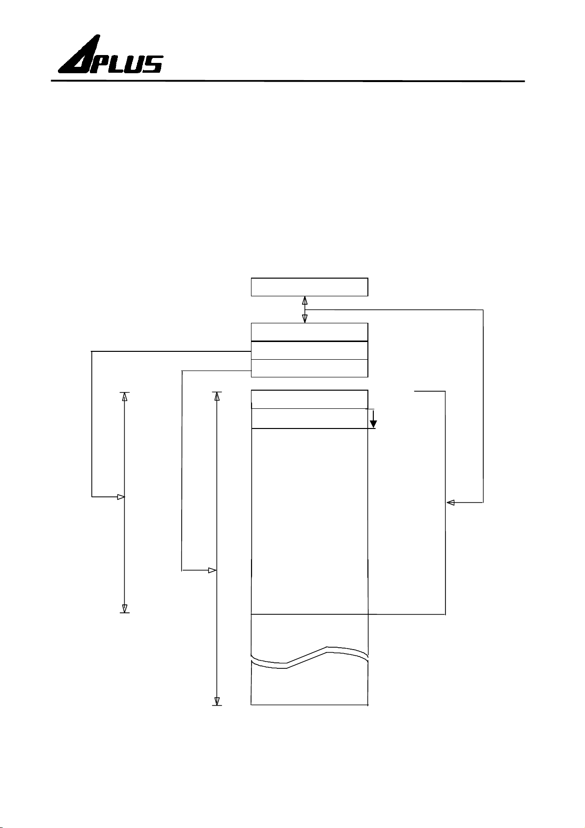
FIGURE 1 : ROM Map of APExx24 Series
PC[15:0]
16-bit x 2 STACK
16-bit Data Pointer
00000h-0FFFFh
Data ROM for Melody
00000h-FFFFFh
Voice RO M for Vo ice
20-bit Voice Pointer
Reserved for Testing
Reset Vector
00000h
000FEh
000FFh-00400h
00401h
00000h-0FFFFh
Program ROM
2
Rev 1.5 2004/4/20
Page 4

3.0 Pin Description
Pad Name Pin Attr. Description
PWM2/Cout
PWM1
Vdd1~3
PRA0~3
PRC0~3
PRD0~3
PRE0~3
PRF0~3
PRB0 / OSC2
PRB1 / IR
PRB2
Power
O
O PWM1 output.
I/O
I/O
I/O
I/O
PWM2 output, or Current Output of Audio.
Power supply during operation.
I/O port can be progr ammed to input/output in dividually.
Input type with weak pull-low or fix-input-floating capability.
Buffer Output type.
I/O port can be configured to input/output individually or HM OSC pad.
Input type with weak pull-low or fix-input-floating capability.
Buffer Output type.
I/O port can be configured to input/output individually.
Input type with weak pull-low or fix-input-floating capability.
Buffer Output type.
Mask option selected as an IR Carrier Output with 38k / 56kHz
I/O port can be configured to input/output individually.
Input type with weak pull-low or fix-input-floating capability.
Buffer Output type.
APExx24 Series
PRB3 / Reset
OSC1
GND1~4
I/O
I
Power
4.0 DC Characteristics
Symbol Parameter Vdd Min. Typ. Max. Unit Condition
Vdd Operating voltage 2.4 3 5.5 V depending on Freq.
Isb Standby
Iop
Iih
Ioh Output-high current
Iol Output-low current
Cout
dF/F Frequency stability -5 5 %
Supply
current
Input current
(Inter n al pu l l lo w)
DAC output current
(8-level option)
I/O port can be configured to input/output individually.
Input type with weak pull-low or fix-input-floating capability.
Buffer Output type.
Mask option selected as an external RESET pin with weak pull-low
capability.
RM/HM mode Oscillator input
Ground Potential
Operating
3 1
4.5 1
3 1
4.5 2.5
3 3
4.5 10
3 -3
4.5 -10
3 7
4.5 19
3 0.8 ~ 4.8
4.5 0.9 ~ 6.5
uA
mA
uA
mA
mA
Input ports with weak
4MHz, RM,
in HALT Mode
4MHz, RM,
IO Floating
pull-low
4MHz, RM
(IO ports)
4MHz, RM
(Full s cale)
Fosc(3v- 2.4v)
Fosc (3v)
dF/F Fosc lot variation -10 10 %
3
Vdd=3V, Rosc=430k,
4MHz
Rev 1.5 2004/4/20
Page 5

APExx24 Series
FIGURE 2 : Frequency vs. Rosc (at 3V)
Resistor (Rosc ohms) 110k 200k 300k 430k
Frequency (MHz)
20
15
14.84 8.25 5.54 3.92
Rosc vs Freq.
14.84
10
Freq. (MHz)
5
0
0 100 200 300 400 500
5.0 Application Circuit
8.25
Rosc (k ohm)
5.54
3.92
4
Rev 1.5 2004/4/20
Page 6

6.0 Bonding Diagram of APE12724 / APE17024
2
5
6
8
9
X
Y
34
33
PRF3
31
32
PRF2 PRF1
30 29
PRF0
PRE3
28
PRE2
27
PRE1
26 25
PRE0
PRD3
24 23
PRD2
PRD1
APExx24 Series
20
22
PRD0
21
PRC3
19
18
PRC2 PRC1 Vdd1
GND1
ROM
1
GND4
GND3
Chip Size : 2330 um x 2872um
Pad Size : 80 um x 80 um
* The IC substrate must be connected to GND.
(0,0)
3
Vdd3
4
PWM2/Cout
Vdd2
OSC1
7
PRB0
PRB1
PRB2
10
PRB3
11
PRA0
12
PRA1
13
PWM1
Pad # Pad Name X Y Pad # Pad Name X Y
1
2
3
4
5
6
7
8
9
10
11
12
13
14
15
16
17
GND4 75 404
GND3 57 293
PWM1 56 145
Vdd3 183 60
PWM2/Cout 467 58
Vdd2 988 86
OSC1 1106 86
PRB0/OSC2 1224 86
PRB1/IR 1342 86
PRB2 1460 86
PRB3/Reset 1578 86
PRA0 1696 86
PRA1 1814 86
PRA2 1932 86
PRA3 2050 86
PRC0 2168 86
GND2 2160 230
18
19
20
21
22
23
24
25
26
27
28
29
30
31
32
33
34
GND1 2033 2703
PRC1 1920 2703
PRC2 1807 2703
PRC3 1694 2703
PRD0 1581 2703
PRD1 1468 2703
PRD2 1355 2703
PRD3 1242 2703
PRE0 1129 2703
PRE1 1016 2703
PRE2 903 2703
PRE3 790 2703
PRF0 676 2703
PRF1 563 2703
PRF2 450 2703
PRF3 337 2703
Vdd1 223 2703
PRA2
14
GND2
PRA3
15
17
PRC0
16
5
Rev 1.5 2004/4/20
Page 7

6.2 Bonding Diagram of APE25524 / APE34024
2
5
6
8
9
X
Y
34
33
PRF3
31
32
PRF2 PRF1
30 29
PRF0
PRE3
28
PRE2
27
PRE1
26 25
PRE0
PRD3
24 23
PRD2
PRD1
APExx24 Series
20
22
PRD0
21
PRC3
19
18
PRC2 PRC1 Vdd1
GND1
ROM
1
GND4
GND3
Chip Size : 2330 um x 4694 um
Pad Size : 80 um x 80 um
* The IC substrate must be connected to GND.
PWM1
3
(0,0)
Vdd3
4
PWM2/Cout
Pad # Pad Name X Y Pad # Pad Name X Y
1
2
3
4
5
6
7
8
9
10
11
12
13
14
15
16
17
GND4 75 404
GND3 58 293
PWM1 56 145
Vdd3 183 60
PWM2/Cout 467 58
Vdd2 988 86
OSC1 1106 86
PRB0/OSC2 1224 86
PRB1/IR 1342 86
PRB2 1460 86
PRB3/Reset 1578 86
PRA0 1696 86
PRA1 1814 86
PRA2 1932 86
PRA3 2050 86
PRC0 2168 86
GND2 2160 230
Vdd2
OSC1
PRB0
7
18
19
20
21
22
23
24
25
26
27
28
29
30
31
32
33
34
PRB1
PRB2
10
PRB3
11
PRA0
12
PRA1
13
GND1 2033 4525
PRC1 1920 4525
PRC2 1807 4525
PRC3 1694 4525
PRD0 1581 4525
PRD1 1468 4525
PRD2 1355 4525
PRD3 1242 4525
PRE0 1129 4525
PRE1 1016 4525
PRE2 903 4525
PRE3 790 4525
PRF0 676 4525
PRF1 563 4525
PRF2 450 4525
PRF3 337 4525
Vdd1 223 4525
PRA2
14
GND2
PRA3
15
17
PRC0
16
6
Rev 1.5 2004/4/20
 Loading...