

Page 1
INTEGRATED CIRCUITS INC.
COMPRESS VOICE --- APC5800M MODULE
Part No. : APC5800M4 & APC5800M2
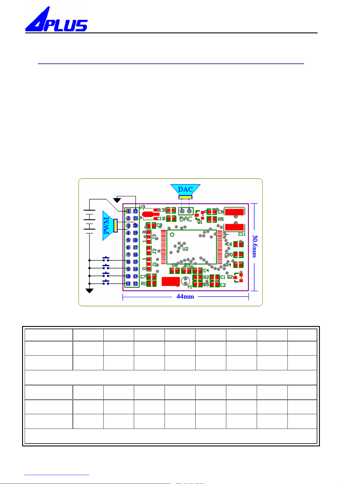
Module size : 32.8 x 45.6 mm
VCC : 4.5V
I/O : PA0 ~ PA7 + PB0 ~ PB7
Speaker output : DAC ( 12 bits ) or PWM
Compress : 6K bps ~ 14.4K bps for VOICE / 10K bps ~ 24K bps for MUSIC
Part no. 6K 7.2K 8.4K 9.6K 10.8K 12K 13.2K 14.4K
APC5800M2 91 min. 75 min. 65 min. 56 min. 50 min. 45 min. 41 min. 37 min.
APC5800M4 182 min. 151 min. 130 min. 113 min. 101 min. 91 min. 82 min. 75 min.
6K bps ~ 14.4 K bps for VOICE compress
Part no. 10K 12K 14K 16K 18K 20K 22K 24K
APC5800M2 54 min. 45 min. 39 min. 34 min. 30 min. 27 min. 24 min. 22 min.
APC5800M4 109 min. 91 min. 78 min. 68 min. 60 min. 54 min. 49 min. 45 min.
10K bps ~ 24K bps for MUSIC compress
http://www.aplusinc.com.tw PAGE / 5 VER1.3
1
Page 2

INTEGRATED CIRCUITS INC.
1 2 3 4 5 6 7 8 9 10 11
VDD4V5
Reset PWM1 PB6 PB4 PB2 PB0 PA6 PA4 PA2 PA0
22 21 20 19 18 17 16 15 14 13 12
GND VDD3V PWM2 DAC PB5 PB3 PB1 PA7 PA5 PA3 PA1
PS: PIN-19 is DAC output for drive OP-AMP,but Q1,R5& C9 must be delete
ADDRESS ARRANGEMENT :
1. RAM
0000-07FF: Internal RAM of 1Kx16
0000-1FFF: External, Non-Bank RAM (Extramcs=1) of 4Kx16
2. ROM
4000-7FFF: Data area for bank select, BANK ROM or BANK RAM, sized with
16K x 16 and even up to 64M-bit
C000-FFFF: for system program or user program of 16Kx16
FFF0, FFF1: executed IRQ vector of copressor
FFF2, FFF3: IRQ vector of ADC
FFF4, FFF5: not used
FFF6, FFF7: IRQ vector of Timer (IRQ vector of Fix_Timer or Timer_A)
FFF8, FFF9: IRQ vector of PA[7:0]
FFFA, FFFB: NMI vector of Timer_B
FFFC, FFFD: RES vector.
FFFE, FFFF: IRQ vector of EXT
According to priority, RES, NMI, OK_INT, ADC_INT, TIMER_INT,
PA_INT, and EXT_IRQ are arranged.
http://www.aplusinc.com.tw PAGE / 5 VER1.3
2
Page 3

INTEGRATED CIRCUITS INC.
Memory Mapping
3FE0 System Flag. Read only
Bit 0: = not used
1: = no used
2: = 1 -- error in ADC
0 -- no error in ADC
3: = 1 Timer_A INT flag
Timer IRQ Timer_A INT flag
1 1 Timer_A INT
1 0 Fix_Timer INT
0 x no Timer INT
4: = 1 (not used)
5: = 1 (executed flag of Coprocessor)
6: = 1 (coprocessor’s carry)
7: = 1 (tone0 or tone1 enabled)
3FE0 System control 0. Write only
Bit 0: = must be 0.
0 --PA14 and PA15 are IO pins (default).
1: = 1-- PB9 is an EXTIRQ pin.
0-- PB9 is an IO pin (default).
2: = 1-- PB7 is EXTRAMCS.
0-- PB7 is an IO pin (default).
3: = 1-- ADC enabled; PA13 is an ADC pin.
0-ADC disabled;PA13 is an IO pin(default).
4: = not used (must be 0.)
5: = not used (must be 0.)
6: = 1-- (PWM enabled)
0 --(PWM disabled (default))
7: = 1--(DAC enabled)
0 --(DAC disabled (default))
http://www.aplusinc.com.tw PAGE / 5 VER1.3
3
Page 4

INTEGRATED CIRCUITS INC.
3FE1 System Control 1. Write only
Bit 0: = 1 -(Timer A clock selects system clock.)
0- (Timer A clock selects 32.768k Hz.) (Default)
1: = not used (must be 0.)
2: = 1-- (Timer A enabled)
0 --(Timer A disabled) (Default)
3: = 1 -- (Timer B enabled)
0-- (Timer B disabled) (Default)
4: = 1--(Timer A interrupt enabled)
0-- (Timer A interrupt disabled) (Default)
5: = 1-- (Timer B NMI enabled)
0 --(Timer B NMI disabled) (Default)
6: = 1-- (System clock = 32768Hz)
0-- (System clock = PLL clock) (Default)
7: = 1-- (Watchdog timer enabled) (Default)
0-- (Watchdog timer disabled)
3FE2 System control 2. Write only
Bit 0: = 1-- (Entry to stand-by mode)
In stand-by mode, CPU is held. The NMI and
IRQ will wake up the CPU.
1: = 1 --(Entry to sleep mode)
In sleep mode, both of the main system clock
and 32768Hz will be stopped, so all functions
are stopped and only an external interrupt can
wake up this chip.
3-2: = 00 (system clock = Fxosc/2 X 256 (4.19MHz)) (Default)
01 (system clock = Fxosc/2 X 512 (8.38MHz))
10 (system clock = Fxosc/2 X 768 (12.58MHz))
7-4: = 0xxx (Fix-timer disabled)
1000 (Fix-timer = 64Hz)
1001 (Fix-timer = 32Hz)
1010 (Fix-timer = 16Hz)
1011 (Fix-timer = 8Hz)
1100 (Fix-timer = 4Hz)
1101 (Fix-timer = 2Hz)
1110 (Fix-timer = 1Hz)
1111 (Fix-timer = 0.5Hz)
3FE3 interrupt enable register of Port_a[7..0]. Write only
A ‘0’ in this register will set the interrupt function of the corresponding pin of port_a to be enabled.
The default value for each bit is ‘1’.
3FE4 data register of Port_a[7..0]. Read and write
3FE5 direction register of Port_a[7..0]. Write only
A ‘1’ in this register will set the corresponding pin of port_a to be output. The
default value for each bit is zero.
3FE6 data register of Port_b[7..0]. Write only
3FE7 Clear watchdog timer. Write only
The watchdog timer reset will happen if the programmer does not clear the
watchdog timer before watchdog timer time-out occurs.
3FE8 Low byte of voice channel 0. Write only
Bit 2-0: Reserved.
Bit 3: not used (must be 0.)
Bit 7-4: = low nibble byte of voice channel 0
3FE9 high byte of voice channel 0. Write only
The resolution of voice channel 0 is 12 bits ($3FE9,$3FE8 bit7_4).
3FEA Bank register for coprocessor. Write only
3FEB Bank register MSB bit for coprocessor. Write only
Bank register is a 9-bit register ($3FEB bit0 and $3FEA bit7-0).
The memory range of bank is from $4000 to $7FFF.
Bit 7-1: Reserved.
3FEC, 3FED Timer A data or tone0 generator. Read and write. After timer_a is enabled,
the timer will start to count down. When timer counts to zero, the timer will count from the
initial value and timer_a IRQ will happen.
The time elapsing = (($3FED,$3FEC)+1) / (Timer A input clock)
http://www.aplusinc.com.tw PAGE / 5 VER1.3
4
Page 5

INTEGRATED CIRCUITS INC.
3FEE
low byte data of Timer B. Read and write
3FEF high byte data of Timer B. Read and write
After timer_b is enabled, the timer will start to count down. When timer counts to zero,
the timer will count from the initial value and timer_b NMI will happen.
The time elapsing = (($3FEF,$3FEE)+1) / (Timer B input clock)
3FF0 direction register of Port_a[15..8]. Write only
A ‘1’ in this register will set the corresponding pin of port_a to be output.
The default value for each bit is zero.
3FF1 data register of Port_a[15..8]. Read and write
3FF2 data register of Port_b[11..8]. Write only
Bit 3-0: pin 11 to pin 8 of Port_b
Bit 7-4 : Reserved
3FF4 Bank register for CPU. Write only
3FF5 MSB bit in bank register for CPU. Write only
Bank register is a 9-bit register ($3FF5 bit0 and $3FF4 bit7-0).
The memory range of bank is from $4000 to $7FFF.
Bit 1: Reserved.
Bit 2: = 1 (Voice0 buffer is transferred to DAC port directly.) (Default)
0 (Voice0 buffer will be transferred to DAC port when timer_b NMI happen.)
Bit 7-3 : Reserved.
3FF6 data register of Port_c[7..0]. Read and write
3FF7 data register of Port_c[15..8]. Read and write
3FF8 direction register of Port_c[7..0]. Write only
A ‘1’ in this register will set the corresponding pin of port_c to be output.
The default value for each bit is zero.
3FF9 direction register of Port_c[15..8]. Write only
A ‘1’ in this register will set the corresponding pin of port_c to be output.
The default value for each bit is zero.
3FFA ADC register. Read only
When the timer b NMI occurs, the A/D conversion process starts and the S/H circuit stops
sampling and begins holding it until the ADC process is finished.
The ADC interrupt will be generated when ADC process is finished.
3FFB, 3FFC, 3FFD….not used
3FFE low byte of Voice channel 1, and system control 3. Write only
Bit 0: = 1 (Mix mode for DAC output)
0 (Separate mode for DAC output) (Default)
1: = 1 (Mix mode for PWM output)
0 (Separate mode for PWM output) (Default)
2: = not used (must be 0.)
3: = not used (must be 0.)
7-4: = low nibble byte of voice channel 1
3FFF high byte of voice channel 1. Write only
The resolution of voice channel 1 is 12 bits ($3FFF and $3FFE bit7_4).
This register will be transferred to PWM port while timer_b NMI happen in a separate mode.
http://www.aplusinc.com.tw PAGE / 5 VER1.3
5
 Loading...