

Page 1

Integrated Circuits Inc. aP89021/010
APLUS MAKE YOUR PRODUCTION A-PLUS
VOICE OTP IC
aP89021 – 21sec
aP89010 – 10sec
APLUS INTEGRATED CIRCUITS INC.
Address:
3 F-10, No. 32, Sec. 1, Chenggung Rd., Taipei,
Taiwan 115, R.O.C.
(115)台北市南港區成功路一段 32 號 3樓之 10.
TEL: 886-2-2782-9266
FAX: 886-2-2782-9255
WEBSITE : http: //www.aplusinc.com.tw
Sales E-mail:
sales@aplusinc.com.tw
Technology E-mail:
service@aplusinc.com.tw
Ver 2.0 Dec 6, 2006
1
Page 2

Integrated Circuits Inc. aP89021/010
FEATURES
l Standard CMOS process.
l Embedded 512K/256K bits EPROM.
l 21/10 Sec Voice Length at 6 KHz sampling and 4-bit ADPCM compression.
l Maximum 12 voice groups.
l Combination of voice building blocks to extend playback duration.
l 960 table entries are available for voice block combinations.
l User selectable PCM or ADPCM data compress.
l Two triggering modes are available by whole chip option during voice compilation.
- Key Trigger Mode – Combinations of S1 ~ S4 to trigger up to 12 voice groups; SBT
for sequential trigger.
- CPU Parallel Trigger Mode – Combinations of S1 ~S4 with SBT goes HIGH to strobe
start the voice playback.
l Voice Group Trigger Options: Edge / Level; Hold / Un-hold; Retrigger / Non-retrigger.
l Whole Chip Options: Ramp / No-ramp; Output Options; Key / CPU trigger mode.
l 16ms (@ 8KHz sampling rate) Debounce Time for both Key and CPU Trigger Modes.
l RST pin set to HIGH to stop playback at once.
l Three user programmable outputs for STOP plus, BUSY signal and flashing LED.
l Built-in oscillator to control sampling frequency with an external resistor.
l 2.2V – 3.6V single power supply and < 5uA low stand-by current.
l PWM Vout1 and Vout2 drive speaker directly.
l D/A COUT to drive speaker through an external BJT.
l Development System support voice compilation and options selection.
DESCRIPTION
aP89021/010 high performance Voice OTP is fabricated with Standard CMOS process with embedded
512K/256K bits EPROM. It can store up to 21/10 sec voice message with 4-bit ADPCM compression
at 6KHz sampling rate. 8-bit PCM is also available as user selectable option. Two trigger modes,
simple Key trigger mode and Parallel CPU trigger mode facilitate different user interface. User
selectable triggering and output signal options provide maximum flexibility to various applications.
Built-in resistor controlled oscillator, 8-bit current mode D/A output and PWM direct speaker driving
output minimize the number of external components. PC controlled programmer and developing
software are available.
Ver 2.0 Dec 6, 2006
2
Page 3
Integrated Circuits Inc. aP89021/010
2 3 4 5 6 7 8
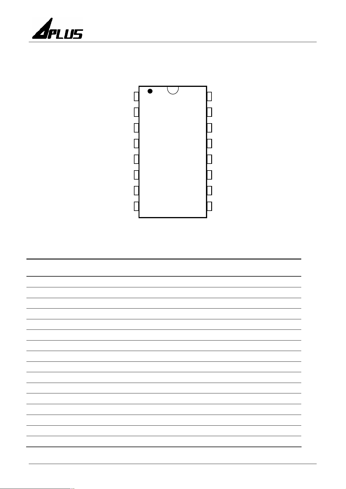
PIN CONFIGURATIONS
PIN NAMES
PIN
Playback
Mode
OUT1
VOUT1
VOUT2
VSS
OUT2
OUT3
COUT
OSC
1
OTP Program
Mode
300 mil DIP
150 mil SOP
Description
16
15
14
13
12
11
10
RST
SBT
S4
S3
VDD
S2
S1
9
VPP
1 OUT1 OEB Programmable output (I/O pin)
2 VOUT1 - PWM output to drive speaker directly
3 VOUT2 - PWM output to drive speaker directly
4 VSS VSS Power Ground
5 OUT2 IO Programmable output (I/O pin)
6 OUT3 - Programmable output (I/O pin)
7 COUT - D/A current output
8 OSC ACLK Oscillator input
9 VPP VPP Supply voltage for OTP programming
10 S1 S1 Trigger pin (input with internal pull-down)
11 S2 S2 Trigger pin (input with internal pull-down)
12 VDD VDD Positive Power Supply
13 S3 S3 Trigger (input with internal pull-down)
14 S4 S4 Trigger (input with internal pull-down)
15 SBT PGM Trigger pin (input with internal pull-down)
16 RST DCLK Reset pin (input with internal pull-down)
Ver 2.0 Dec 6, 2006
3
Page 4

Integrated Circuits Inc. aP89021/010
PIN DESCRIPTIONS
S1 ~ S4
Input Trigger Pins:
- S1 to S4 are used to trigger the 12 Voice Groups in both Key and CPU Parallel Trigger Mode.
- In OTP Programming Mode, S1 to S4 are used as program enable pins.
SBT
Input Trigger Pin:
- In Key Trigger Mode, this pin is trigger pin to trigger the playback of Voice Groups one by one
sequentially.
- In CPU Parallel Command Mode, this pin is used as address strobe to latch the input from S1 to
S4 and starts the voice playback.
- In OTP Programming Mode, this pin is used as PGM signal.
VDD
Power Supply Pin.
VSS
Power Ground Pin
VOUT1 and VOUT2
Digital PWM output pins which can drive speaker and buzzer directly for voice playback.
OSC
During voice playback, an external resistor is connected between this pin and the VDD pin to set the
sampling frequency. In OTP Programming Mode, this is the ACLK input signal.
VPP
Connection to VDD is required during voice playback. In OTP Programming Mode, this pin is
connected to a separate 6.5V power supply.
OUT1, OUT2 and OUT3
- In Key Trigger Mode and CPU Parallel Command Mode, these pins are user programmable pins
for the STOP pulse, BUSY and LED signals.
- During OTP programming, OUT1 serves as OEB while OUT2 serves as data IO.
COUT
Analog 8-bit current mode D/A output for voice playback
RST
Chip reset in playback mode or DCLK pin in OTP programming mode.
Ver 2.0 Dec 6, 2006
4
Page 5
Integrated Circuits Inc. aP89021/010
VOICE SECTION COMBINATIONS
Voice files created by the PC base developing system are stored in the built-in EPROM of the
aP89021/010 chip as a number of fixed length Voice Blocks. Voice Blocks are then selected and
grouped into Voice Groups for playback. Up to 12 Voice Groups are allowed. A Voice Block Table
is used to store the information of combinations of Voice Blocks and then group them together to form
Voice Group.
Chip aP89021 aP89010
Memory size 512K bits 256K bits
Max no. of Voice Block 126 124
No. of bytes per Voice Block 512 256
Max. no. of Voice Group 12 12
No. of Voice Table entries 960 960
Voice Length (@ 6KHz 4-bit ADPCM) 21 sec 10 sec
Example of Voice Block Combination
Assume here we have three voice files, they are “How are You?”, Sound Effect and Music. Each of
the voice file is divided into a number of fixed length Voice Block and stored into the memory.
Voice File 1 - “How are You?” is stored in Voice Block B0 to B12.
Voice File 2 - Sound Effect is stored in Voice Block B13 to B15.
Voice File 3 - Music is Voice Block B16 to B40.
Voice Blocks are grouped together using Voice Table to form Voice Group for playback:
Group no. Voice Group contents Voice Table Entries
Group 1 “How are You?” B0 … B12
Group 2 Sound Effect + “How are You?” B13 … B15 + B0 … B12
Group 3 “How are You?” + Music B0 … B12 + B16 … B40
Group 4 Music B16 … B40
Voice Data Compression
Voice File data is stored in the on-chip EPROM as either 4-bit ADPCM or 8-bit PCM format. Voice
data stored as 4-bit ADPCM provides 2:1 data compression which can save 50% of memory space.
On the other hand, voice data are stored as 8-bit PCM format means no data compression is employed
but voice playback quality will be better.
Ver 2.0 Dec 6, 2006
5
Page 6
Integrated Circuits Inc. aP89021/010
Programmable Options
In both Key Trigger Mode and CPU Parallel Trigger Mode, user can select different trigger functions
and output signals to be sent out from the pins OUT1, OUT2 and OUT3.
Options affect all Voice Group playback are called Whole Chip Options. Options only affect the
playback of individual Voice Group are called Group Options.
Whole Chip Options
• Key or CPU Parallel Trigger Mode.
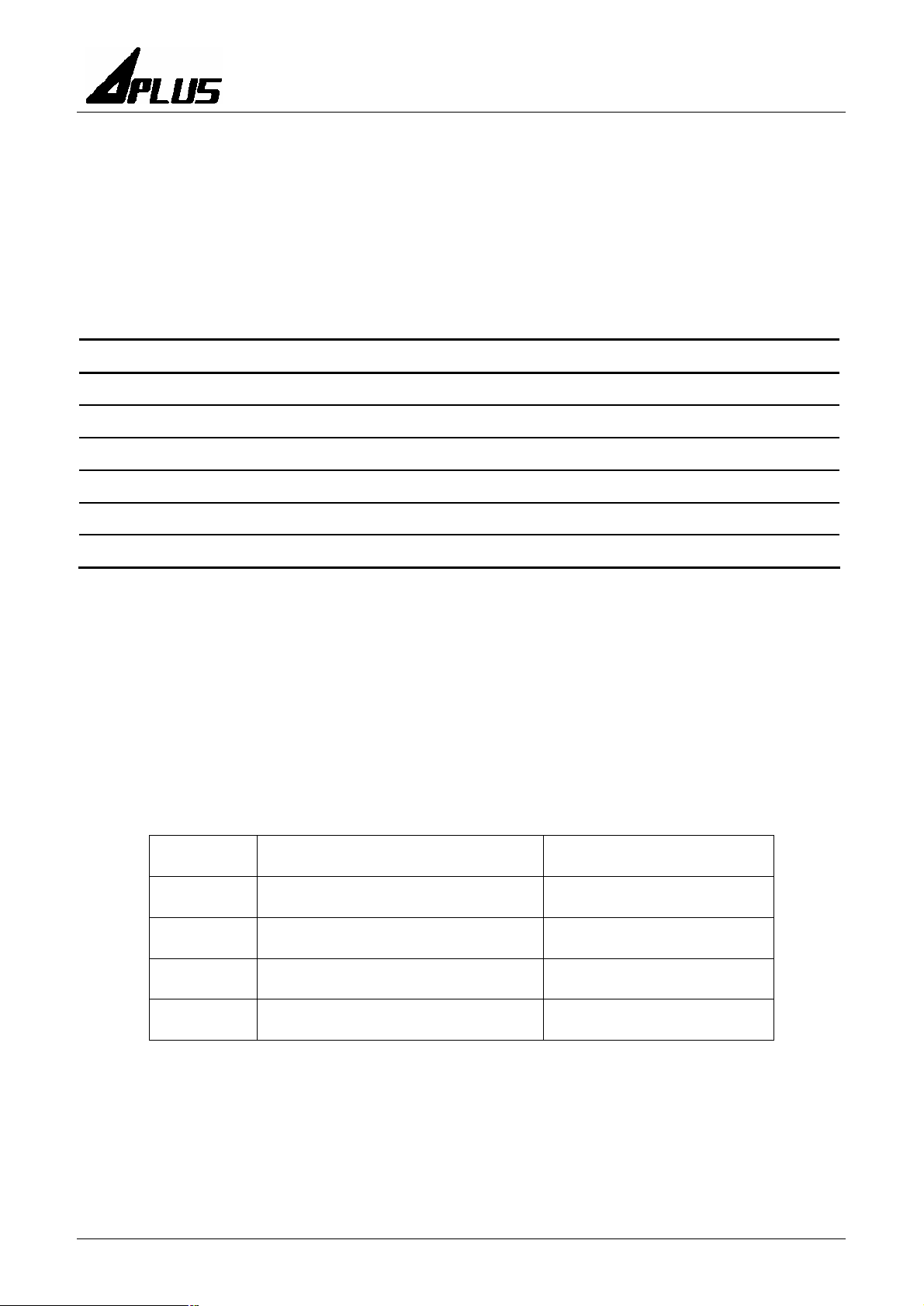
• Ramp-up-down enable or disable:
When COUT is used for playback, Ramp-up-down should be enabled. This function eliminates
the ‘POP’ noise at the beginning and end of voice playback.
When VOUT1 and VOUT2 are used to drive speaker directly, Ramp-up-down should be
disabled.
Fig. 1 Ramp-up-down Enable Fig.2 Ramp-up-down Disable
• Output Options:
This option sets up the three output pins OUT1 and OUT2 to send out different signals during
voice playback. Four settings are allowed:
OUT1 OUT2 OUT3
Option 1 LED2 LED1 BUSY
Option 2 STOP LED1 LED2
Option 3 LED1 BUSY STOP
Note: Stop plus must be set to enable in order to have STOP plus to come
out. The BUSY output is always HIGH during voice playback.
Fig. 3 Output waveforms
Ver 2.0 Dec 6, 2006
6
Page 7
Integrated Circuits Inc. aP89021/010
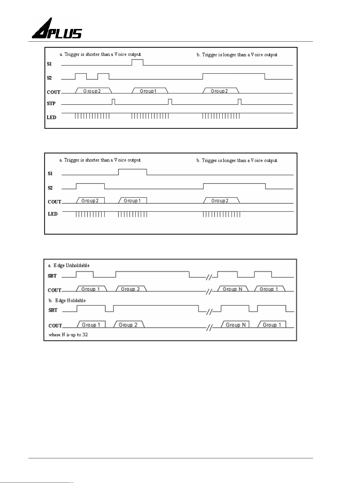
Group Options
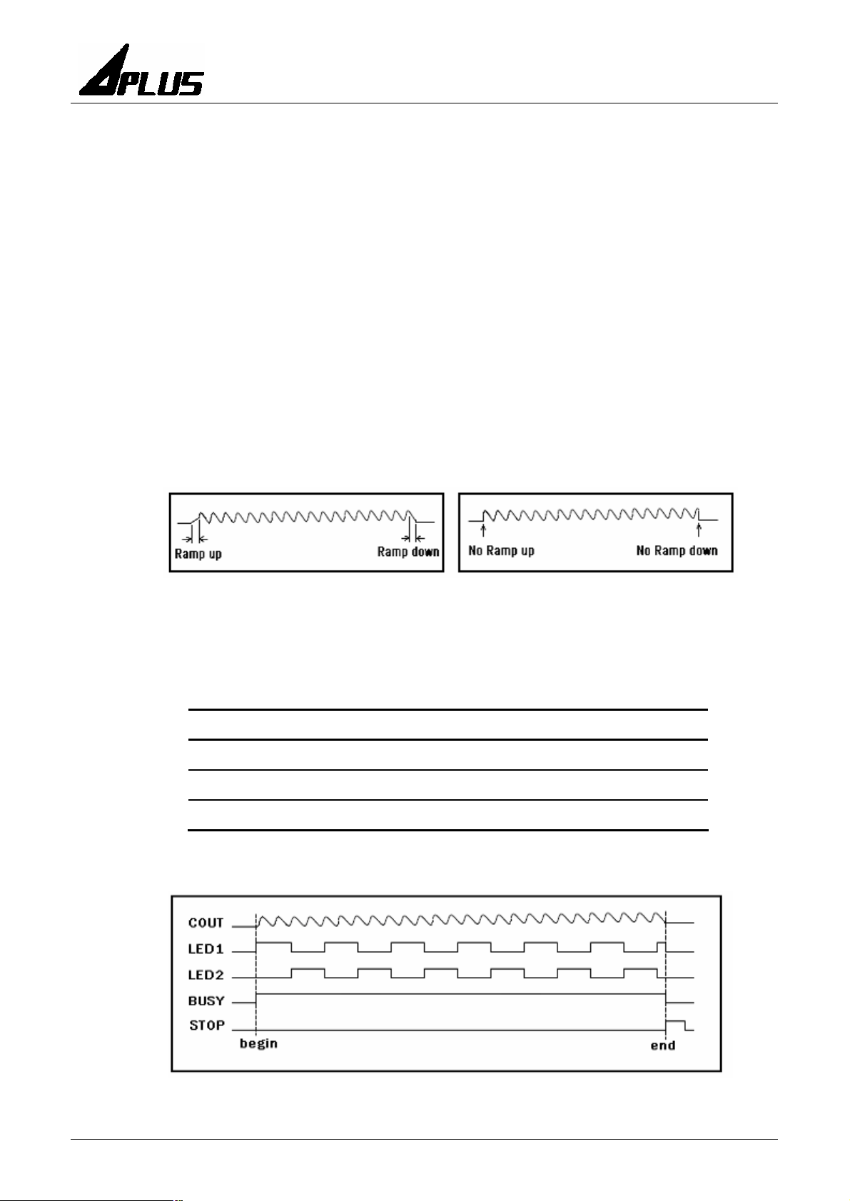
User selectable options that affect each individual group are called Group Options. They are:
• Edge or Level trigger
• Unholdable or Holdable trigger
• Re-triggerable or non-retriggerable
• Stop pulse disable or enable
Fig. 4 to Fig. 9 show the voice playback with different combination of triggering mode and the
relationship between outputs and voice playback.
Fig. 4 Level, Unholdable, Non-retriggerable
Fig. 5 Level Holdable
Fig. 6 SBT sequential trigger with Level Holdable and Unholdable
Ver 2.0 Dec 6, 2006
7
Page 8
Integrated Circuits Inc. aP89021/010
Fig. 7 Edge, Unholdable, Non-retrigger
Fig. 8 Edge, Holdable
Fig. 9 SBT sequential trigger with Edge Holdable and Unholdable
Ver 2.0 Dec 6, 2006
8
Page 9
Integrated Circuits Inc. aP89021/010
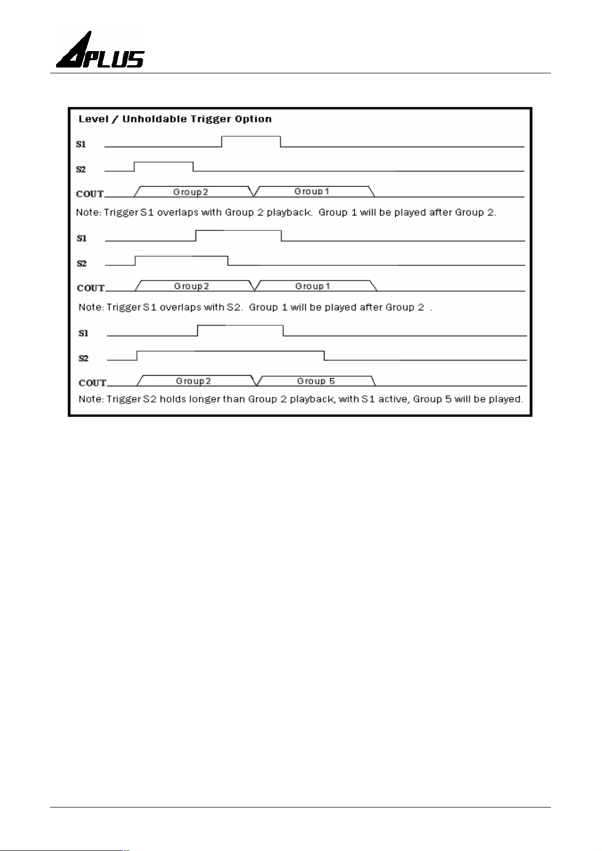
Overlap trigger is supported with Level/Unholdable trigger options:
Fig. 10 Overlap trigger
Ver 2.0 Dec 6, 2006
9
Page 10
Integrated Circuits Inc. aP89021/010
TRIGGER MODES
There are two triggering modes available for aP89021/010.
Key or CPU Trigger modes are determined by setting the EPORM programmable options during voice
data compilation.
Key Trigger Mode
With this trigger mode, up to 12 Voice Groups are triggered by setting S1 to S4 to HIGH or NC (not
connected) in different combinations. Each Voice Group can have its only independent trigger options
(See Fig. 4, 5, 7 and 8 for trigger options definition).
Voice Groups can also be triggered sequentially by setting SBT pin to HIGH.
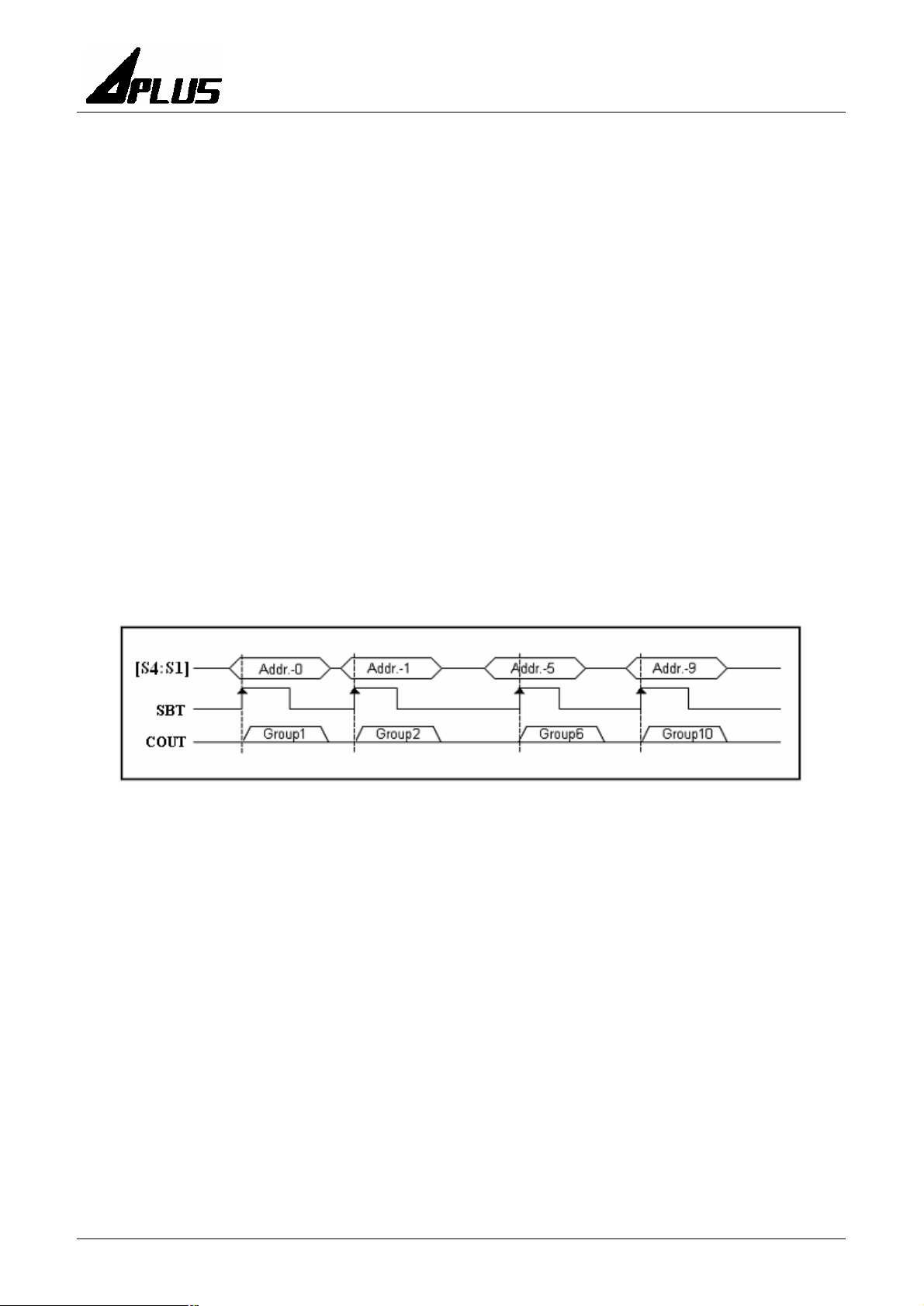
CPU Parallel Trigger Mode
In this mode, S1 to S4 are set to HIGH or LOW according to the table on the following page and
followed by setting the SBT input pin to HIGH, the corresponding Voice Group will be triggered.
Trigger options defined in Fig. 4, 5, 7 and 8 are valid for this mode.
Fig. 11 CPU Parallel Trigger Mode
Note that SBT pin cannot be used as Single Button Sequential trigger in this mode. In stead, it acts as
a Strobe input to clock-in the data input from S1 to S4 into the chip.
Ver 2.0 Dec 6, 2006
10
Page 11
Integrated Circuits Inc. aP89021/010
Key Trigger Mode
Up to 12 Voice Groups can be triggered by S1 to S4.
Voice Group
1 HIGH NC NC NC
2 NC HIGH NC NC
3 NC NC HIGH NC
4 NC NC NC HIGH
5 HIGH HIGH NC NC
6 NC HIGH HIGH NC
7 NC NC HIGH HIGH
8 HIGH NC NC HIGH
9 HIGH HIGH HIGH NC
10 NC HIGH HIGH HIGH
11 HIGH NC HIGH HIGH
12 HIGH HIGH NC HIGH
CPU Trigger Mode
Up to 12 Voice Groups can be triggered by supplying address to [S4:S1] with SBT as strobe signal.
Voice Group
1 0 0 0 0
2 0 0 0 1
S1 S2 S3 S4
S4 S3 S2 S1
3 0 0 1 0
4 0 0 1 1
5 0 1 0 0
6 0 1 0 1
7 0 1 1 0
8 0 1 1 1
9 1 0 0 0
10 1 0 0 1
11 1 0 1 0
12 1 0 1 1
Ver 2.0 Dec 6, 2006
11
Page 12
Integrated Circuits Inc. aP89021/010
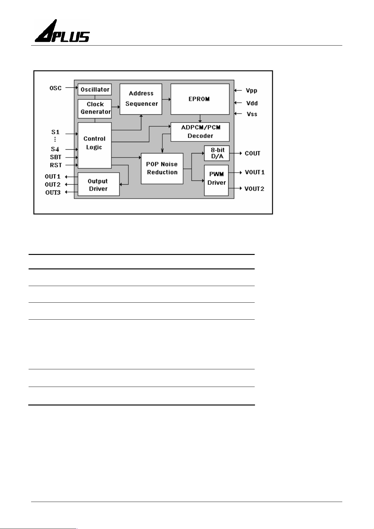
BLOCK DIAGRAM
ABSOLUTE MAXIMUM RATINGS
Symbol Rating Unit
VDD - VSS -0.5 ~ +4.5 V
VIN V
V
T (Operating):
T (Junction) -40 ~ +125
T (Storage) -55 ~ +125
V
OUT
DIP
SOP
- 0.3<VIN<V
SS
SS <VOUT<VDD
-10 ~ +70
-40 ~ +85
+ 0.3 V
DD
V
℃
℃
℃
Ver 2.0 Dec 6, 2006
12
Page 13
Integrated Circuits Inc. aP89021/010
DC CHARACTERISTICS ( T
Symbol Parameter Min. Typ. Max.
= 0 to 70℃, VDD = 3.3V, VSS = 0V )
A
Unit Condition
VDD Operating Voltage 2.2 3.0 3.6 V
ISB Standby current
IOP Operating current
1 5 μA
15 mA
I/O open
I/O open
VIH "H" Input Voltage 2.5 3.0 3.5 V VDD=3.0V
VIL "L" Input Voltage -0.3 0 0.5 V VDD=3.0V
IOL V
IOH V
ICO C
IOH O/P high Current
low O/P Current
OUT
high O/P Current
OUT
O/P Current
OUT
120
-120
-3
-8
mA
mA
mA
mA
Vout=0.3V, VDD=3.0V
Vout=2.5V, VDD=3.0V
V
COUT
VOH=2.5V, VDD=3.0V
=1.0V, VDD=3.0V
IOL O/P low Current
∆F/F
Frequency Stability -5
8
mA
VOL=0.3V, VDD=3.0V
Fosc(3.4V) - Fosc(2.7V)
+5 % Fosc(3V)
Ver 2.0 Dec 6, 2006
13
Page 14
Integrated Circuits Inc. aP89021/010
S1~S
4
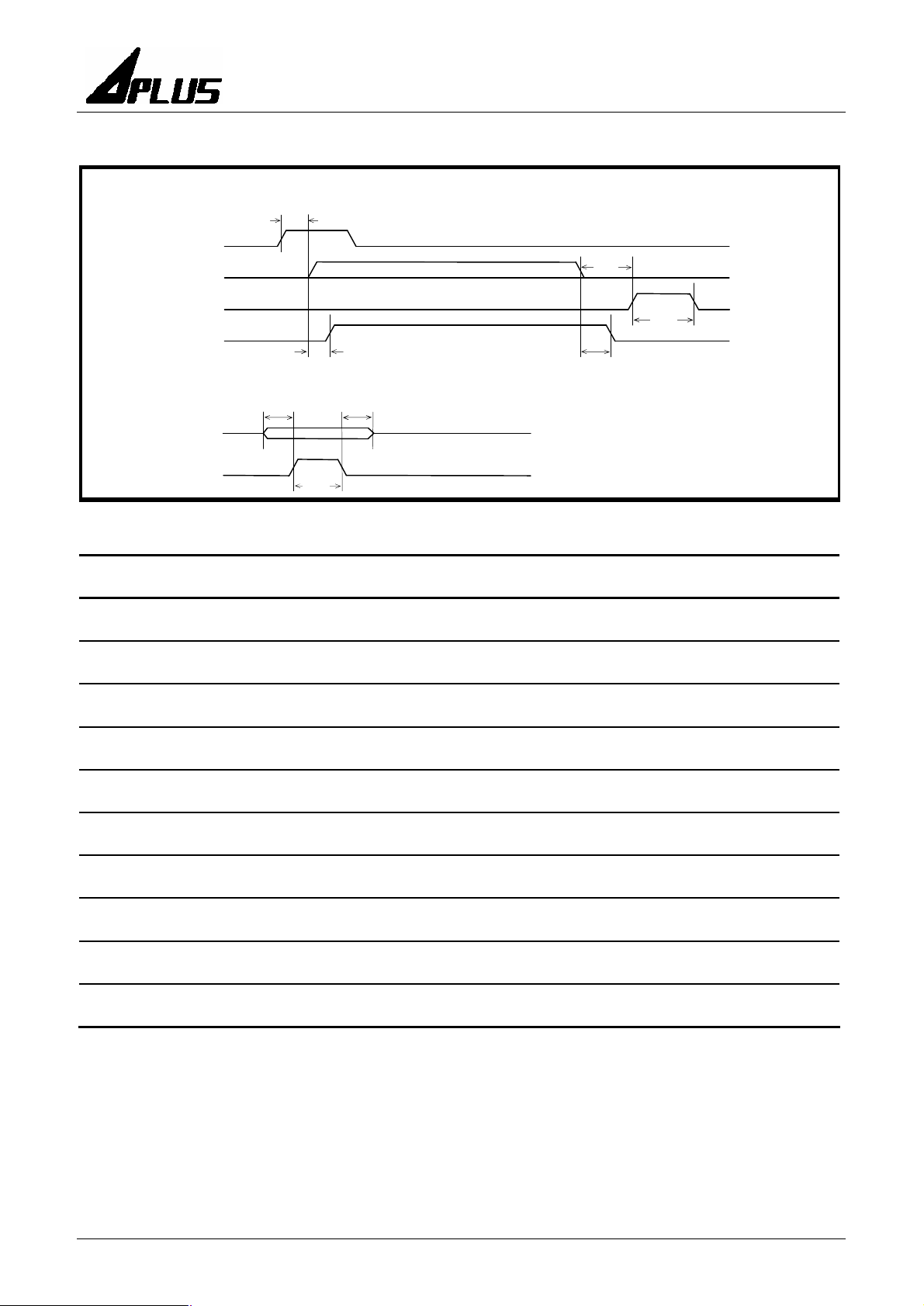
TIMING WAVEFORMS
KEY Trigger Mode
S1~S4, SBT
COUT
tKD
tSTPD
STOP
BUSY
tBD
tBH
CPU Parallel Mode
Addr.
SBT
tAS
tSBTW
tAH
AC CHARACTERISTICS ( T
Symbol Parameter Min. Typ. Max.
tKD Key trigger debounce time 16
tKD Key trigger debounce time – retrigger 24
t
STPD
t
STPW
STOP pulse output delay time
STOP pulse width
= 0 to 70℃, VDD = 3.3V, VSS = 0V, 8KHz sampling )
A
64
tSTPW
Unit Note
ms
ms
256 μs
ms
1
1
1
tBD BUSY signal output delay time
tBH BUSY signal output hold time
tAS Address set-up time 100
tAH Address hold time 100
t
SBTW
t
LEDC
SBT stroke pulse width 16
LED flash frequency
100
3
Notes :
1. This parameter is inversely proportional to the sampling frequency.
2. This parameter is proportional to the sampling frequency.
100 ns
ns
ns
ns
ms
Hz
1
2
Ver 2.0 Dec 6, 2006
14
Page 15
Integrated Circuits Inc. aP89021/010
OSCILLATOR RESISTANCE TABLE
Sampling Frequency
R
OSC
KHz KOhm
4.90
5.26
5.88
300
290
280
6.09 270 110 13.33
6.33 260 100 14.51
6.67 250 91 15.63
6.85 240 82 16.95
7.14 230 75 18.18
7.46 220 68 19.23
7.70 210 62 20.83
8.06 200 56 22.22
8.47 190 51 23.81
8.93 180 43 25.00
9.26 170
9.80 160
10.42 150
Note: The data in the above tables are within 3% accuracy and measured at VDD = 3.0V. Oscillator frequency is
subjected to IC lot to lot variation.
R
OSC
KOhm KHz
Sampling Frequency
140 11.00
130 11.76
120 12.50
Ver 2.0 Dec 6, 2006
15
Page 16
Integrated Circuits Inc. aP89021/010
S1 S2 S3 S4
S1 S2 S3 S4
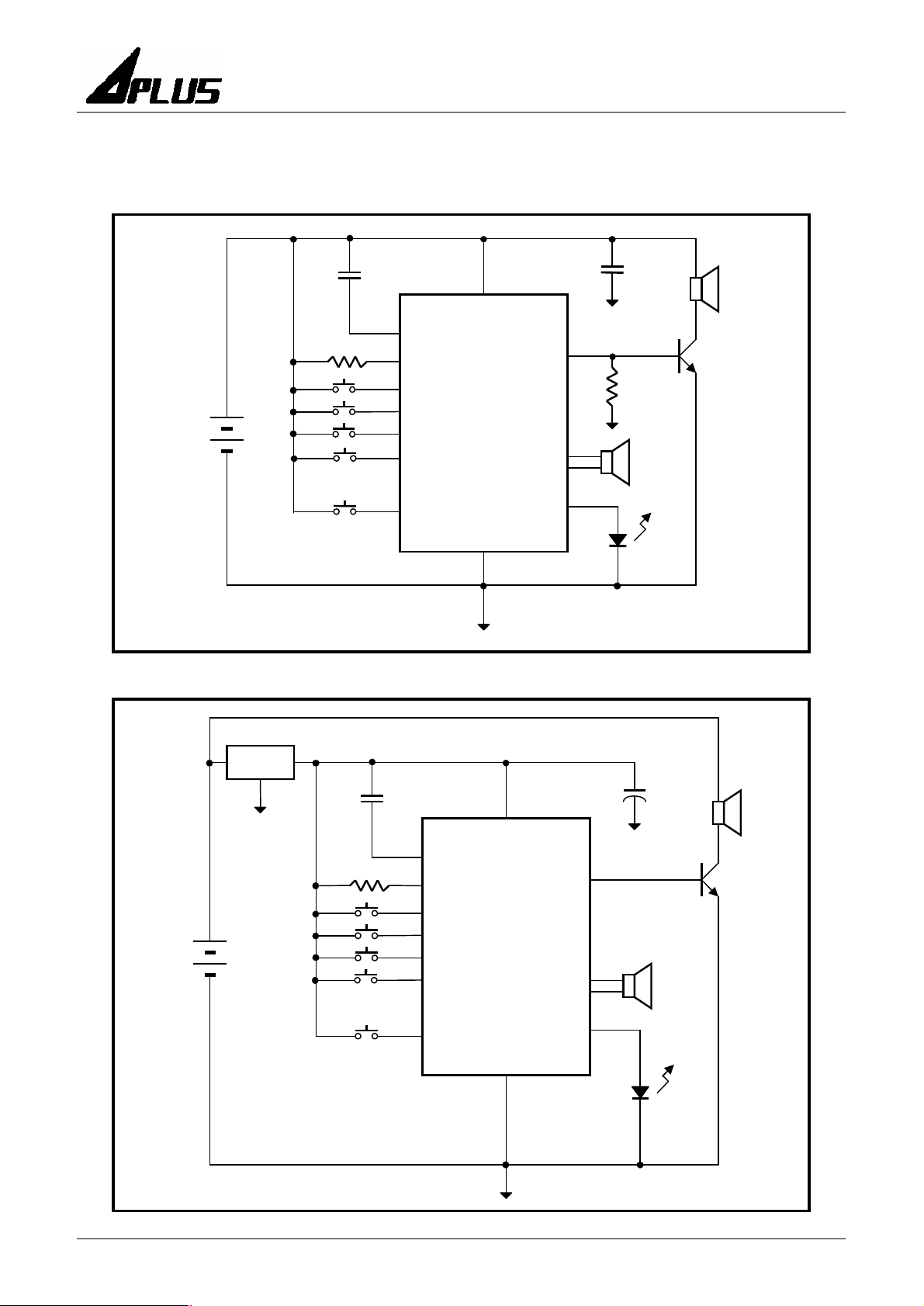
TYPICAL APPLICATIONS
Key Trigger Mode
0.1uF
0.1uF
8Ω
Speaker
VDD,VPP
ROSC
RST
OSC
COUT
8050D
390Ω
3.3V
SBT
VOUT1
VOUT2
OUT1
8 / 16Ω
Speaker
VSS
Fig. 12 Using 3.3V Battery
4.5V
HT7335
ROSC
Output driving of HT LDO:
HT7136 (30mA, 3.6V)
HT7133 (30mA, 3.3V)
HT7536 (100mA, 3.6V)
HT7335 (250mA, 3.5V)
Fig. 13 Using 4.5V Battery
0.1uF
RST
OSC
SBT
VDD,VPP
VOUT1
VOUT2
VSS
COUT
OUT1
10uF
8 / 16Ω
Speaker
8Ω
Speaker
8050D
Ver 2.0 Dec 6, 2006
16
Page 17
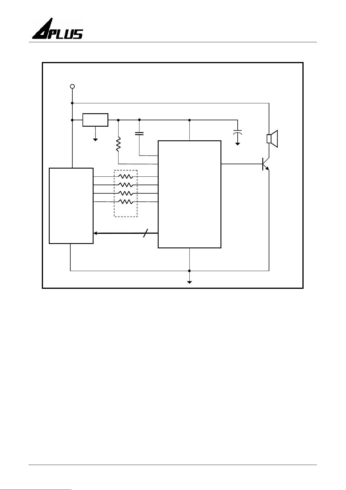
CPU Parallel Mode
S4
S1 S2 S3
VIN=+5V
Integrated Circuits Inc. aP89021/010
VOUT=+3.5V
HT7335
10uF
8Ω
Speaker
ROSC
0.1uF
VDD,VPP
MCU
Addr[0]
Addr[1]
Addr[2]
Addr[3]
Rin
I[0..2]
Rin = 860KΩ x (VIN-VOUT) / VIN
Fig. 14 5V CPU Control with COUT
3
RST
OSC
OUT[1..3]
VSS
COUT
8050D
Ver 2.0 Dec 6, 2006
17
Page 18
Integrated Circuits Inc. aP89021/010
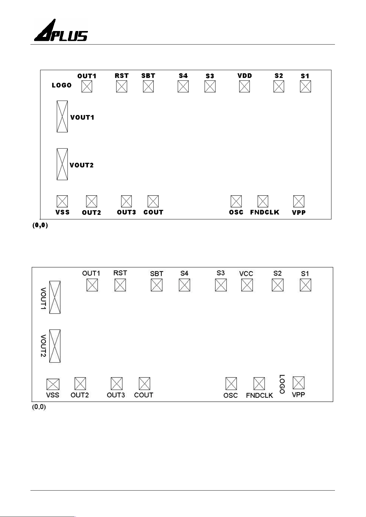
Bonding Diagram (aP89021)
Bonding Diagram (aP89010)
Note: Substrate should be connected to Vss.
Bonding pad size: 80um x 90um
Ver 2.0 Dec 6, 2006
18
 Loading...