

Page 1

ADC12D040
Dual 12-Bit, 40 MSPS, 600 mW A/D Converter with
Internal/External Reference
ADC12D040 Dual 12-Bit, 40 MSPS, 600 mW A/D Converter with Internal/External Reference
November 2003
General Description
The ADC12D040 is a dual, low power monolithic CMOS
analog-to-digital converter capable of converting analog input signals into 12-bit digital words at 40 Megasamples per
second (MSPS), minimum. This converter uses a differential,
pipeline architecture with digital error correction and an onchip sample-and-hold circuit to minimize die size and power
consumption while providing excellent dynamic performance. Operating on a single 5V power supply, the
ADC12D040 achieves 10.9 effective bits at 10 MHz input
and consumes just 600 mW at 40 MSPS, including the
reference current. The Power Down feature reduces power
consumption to 75 mW.
The differential inputs provide a full scale differential input
swing equal to 2V
input. Full use of the differential input is recommended for
optimum performance. The digital outputs for the two ADCs
are available on separate 12-bit buses with an output data
format choice of offset binary or 2’s complement.
For ease of interface, the digital output driver power pins of
the ADC12D040 can be connected to a separate supply
voltage in the range of 2.4V to the digital supply voltage,
making the outputs compatible with low voltage systems.
The ADC12D040’s speed, resolution and single supply operation make it well suited for a variety of applications.
This device is available in the 64-lead TQFP package and
will operate over the industrial temperature range of −40˚C to
+85˚C.
with the possibility of a single-ended
REF
Features
n Binary/2’s complement output format
n Single supply operation
n Internal sample-and-hold
n Outputs 2.4V to 5V compatible
n TTL/CMOS compatible inputs/outputs
n Power down mode
n On-chip reference buffer
n Internal/External Reference
Key Specifications
n Resolution 12 Bits
n Conversion Rate 40 MSPS (min)
n SNR (f
n ENOB (f
n SFDR (f
n Crosstalk 80 dB (typ)
n Data Latency 6 Clock Cycles
n Supply Voltage +5V
n Power Consumption, Operating 600 mW (typ)
= 10 MHz) 68 dB (typ)
IN
= 10 MHz) 10.9 bits (typ)
IN
= 10 MHz) 80 dB (typ)
IN
±
5%
Applications
n Ultrasound and Imaging
n Instrumentation
n Communications Receivers
n Sonar/Radar
n xDSL
n Cable Modems
n DSP Front Ends
TRI-STATE®is a registered trademark of National Semiconductor Corporation.
© 2003 National Semiconductor Corporation DS200460 www.national.com
Page 2
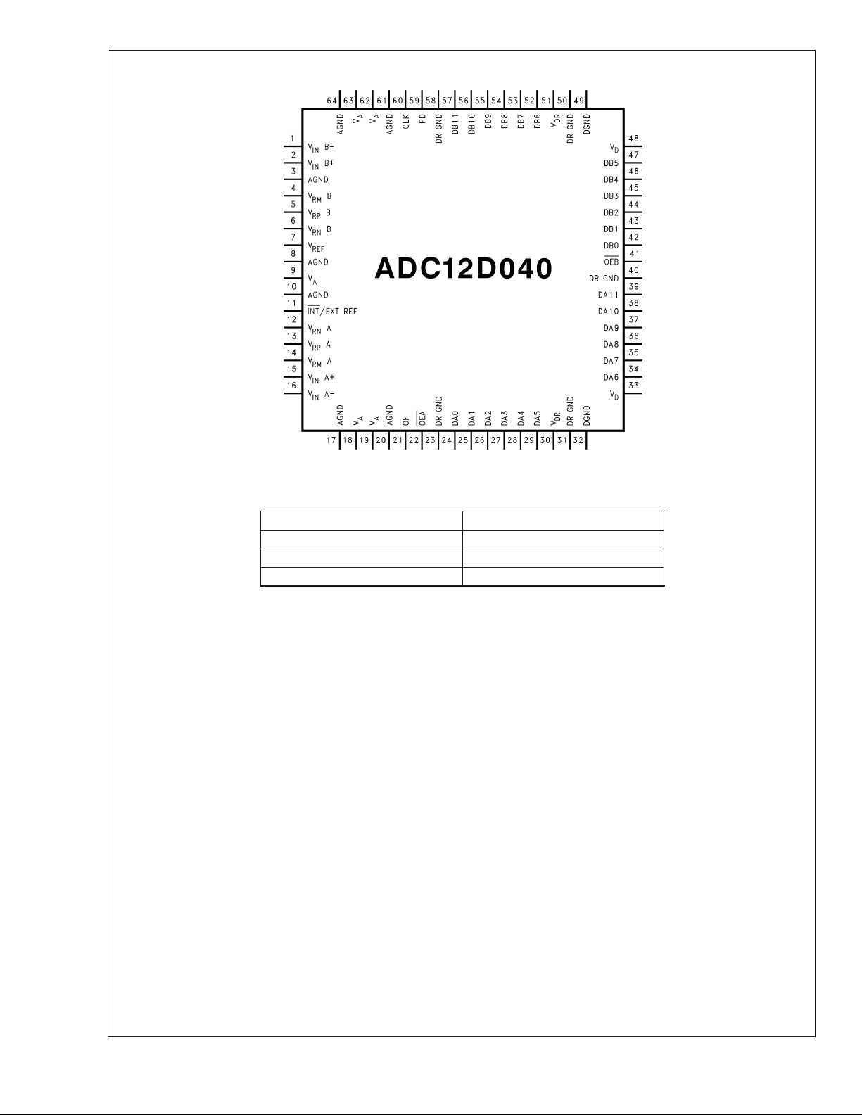
Connection Diagram
ADC12D040
20046001
Ordering Information
Industrial (−40˚C ≤ TA≤ +85˚C) Package
ADC12D040CIVS 64 Pin TQFP
ADC12D040CIVSX 64 Pin TQFP Tape and Reel
ADC12D040EVAL Evaluation Board
www.national.com 2
Page 3
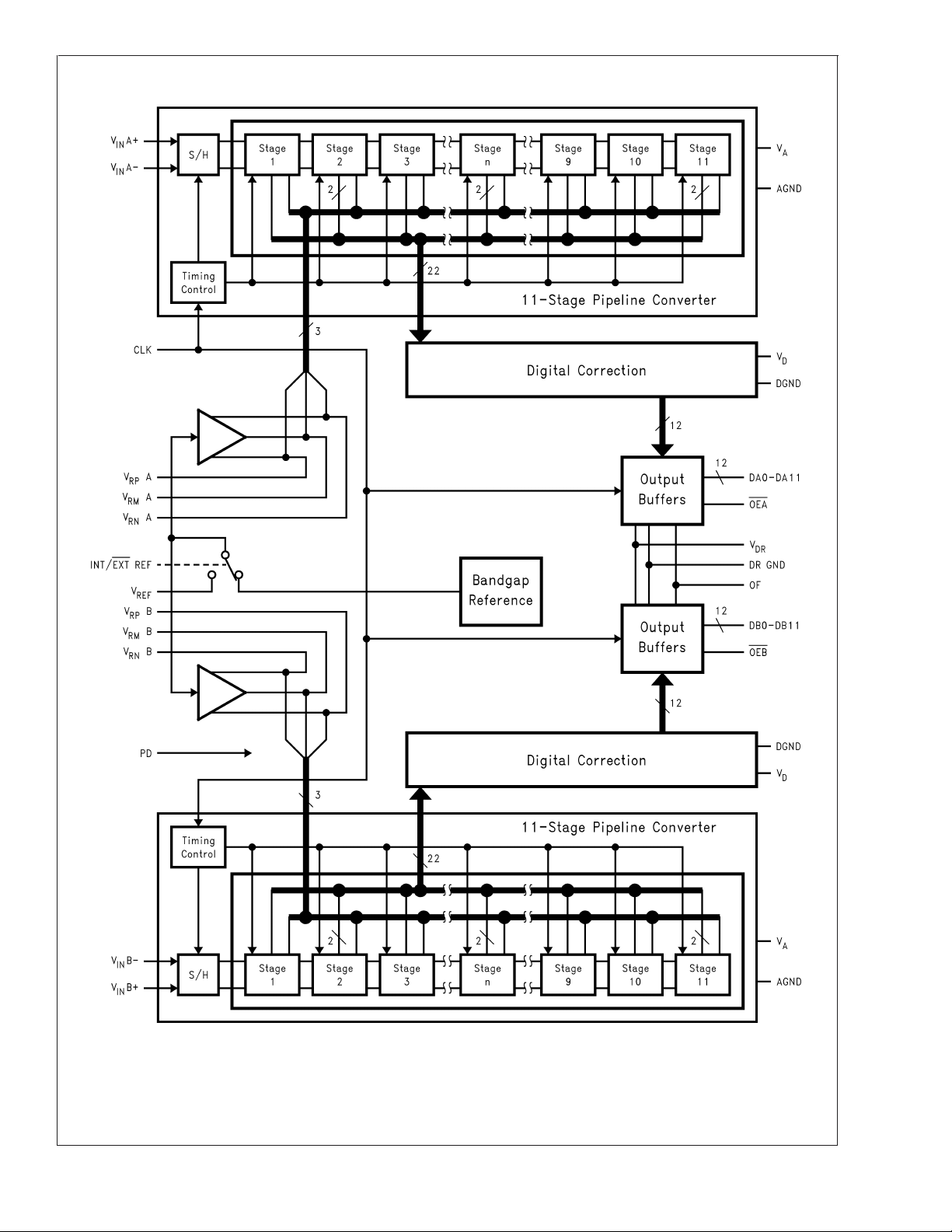
Block Diagram
ADC12D040
www.national.com3
20046002
Page 4
Pin Descriptions and Equivalent Circuits
Pin No. Symbol Equivalent Circuit Description
ANALOG I/O
ADC12D040
15
2
16
1
7V
11 INT/EXT REF
V
A+
IN
B+
V
IN
A−
V
IN
B−
V
IN
REF
Non-Inverting analog signal Inputs. With a 2.0V reference the
full-scale input signal level is 2.0 V
pair, centered on a common V
Inverting analog signal Input. With a 2.0V reference the
full-scale input signal level is 2.0 V
pair, centered on a common V
connected to a common V
a differential input signal is required for best performance.
Reference input. This pin should be bypassed to AGND with
a 0.1 µF monolithic capacitor when external reference is
used. V
is 2.0V nominal and should be between 1.0V to
REF
2.4V.
V
select pin. With a logic low at this pin the internal 2.0V
REF
reference is selected. With a logic high on this pin an external
reference voltage must be applied to V
on each pin of the input
P-P
.
CM
on each pin of the input
P-P
. These (-) input pins may be
CM
for single-ended operation, but
CM
input pin 7.
REF
13
5
14
4
12
6
DIGITAL I/O
60 CLK
22
41
59 PD
21 OF
V
RP
V
RP
V
RM
V
RM
V
RN
V
RN
OEA
OEB
A
B
A
B
These pins are high impedance reference bypass pins only.
Connect a 0.1 µF capacitor from each of these pins to AGND.
DO NOT LOAD these pins.
A
B
Digital clock input. The range of frequencies for this input is
100 kHz to 55 MHz (typical) with guaranteed performance at
40 MHz. The input is sampled on the rising edge of this input.
OEA and OEB are the output enable pins that, when low,
enables their respective TRI-STATE®data output pins. When
either of these pins is high, the corresponding outputs are in a
high impedance state.
PD is the Power Down input pin. When high, this input puts
the converter into the power down mode. When this pin is
low, the converter is in the active mode.
Output Format pin. A logic low on this pin causes output data
to be in offset binary format. A logic high on this pin causes
the output data to be in 2’s complement format.
www.national.com 4
Page 5
Pin Descriptions and Equivalent Circuits (Continued)
Pin No. Symbol Equivalent Circuit Description
ADC12D040
24–29
34–39
DA0–DA11
Digital data output pins that make up the 12-bit conversion
results of their respective converters. DA0 and DB0 are the
LSBs, while DA11 and DB11 are the MSBs of the output
word. Output levels are TTL/CMOS compatible.
42–47
52–57
DB0–DB11
ANALOG POWER
Positive analog supply pins. These pins should be connected
9, 18, 19,
62, 63
V
A
to a quiet +5V source and bypassed to AGND with 0.1 µF
monolithic capacitors located within 1 cm of these power pins,
and with a 10 µF capacitor.
3, 8, 10,
17, 20, 61,
AGND The ground return for the analog supply.
64
DIGITAL POWER
Positive digital supply pin. This pin should be connected to
33, 48 V
D
the same quiet +5V source as is V
DGND with a 0.1 µF monolithic capacitor located within 1 cm
of the power pin and with a 10 µF capacitor.
32, 49 DGND The ground return for the digital supply.
Positive digital supply pins for the ADC12D040’s output
drivers. These pins should be connected to a voltage source
of +2.4V to +5V and bypassed to DR GND with a 0.1 µF
30, 51 V
DR
monolithic capacitor. If the supply for these pins are different
from the supply used for V
and VD, they should also be
A
bypassed with a 10 µF tantalum capacitor. V
exceed the voltage on V
. All bypass capacitors should be
D
located within 1 cm of the supply pin.
The ground return for the digital supply for the ADC12D040’s
23, 31, 40,
50, 58
DR GND
output drivers. These pins should be connected to the system
digital ground, but not be connected in close proximity to the
ADC12D040’s DGND or AGND pins. See Section 5 (Layout
and Grounding) for more details.
and be bypassed to
A
should never
DR
www.national.com5
Page 6
Absolute Maximum Ratings (Notes 1,
2)
If Military/Aerospace specified devices are required,
ADC12D040
please contact the National Semiconductor Sales Office/
Distributors for availability and specifications.
V
A,VD,VDR
V
DR
|V
| ≤ 100 mV
A–VD
Voltage on Any Input or Output Pin −0.3V to (V
6.5V
VD+ 0.3V
or V
A
D
Operating Ratings (Notes 1, 2)
Operating Temperature −40˚C ≤ T
Supply Voltage (V
Output Driver Supply (V
V
Input 1.0V to 2.4V
REF
CLK, PD, OE
Analog Input Pins −0V to (V
|AGND–DGND| ≤100mV
) +4.75V to +5.25V
A,VD
) +2.35V to V
DR
−0.5V to (VD+ 0.5V)
+0.3V)
Input Current at Any Pin (Note 3)
Package Input Current (Note 3)
Package Dissipation at T
= 25˚C See (Note 4)
A
±
25 mA
±
50 mA
ESD Susceptibility
Human Body Model (Note 5) 2500V
Machine Model (Note 5) 250V
Soldering Temperature,
Infrared, 10 sec. (Note 6) 235˚C
Storage Temperature −65˚C to +150˚C
Converter Electrical Characteristics
Unless otherwise specified, the following specifications apply for AGND = DGND = DR GND = 0V, VAVD+5V, VDR+3.0V, PD
= 0V, INT/EXT = V
TJ=T
MIN
to T
MAX
D,VREF
: all other limits TJ= 25˚C (Notes 7, 8, 9)
= +2.0V, OEA, OEB = 0V, f
Symbol Parameter Conditions
STATIC CONVERTER CHARACTERISTICS
Resolution with No Missing Codes 12 Bits (min)
INL Integral Non Linearity (Note 11)
DNL Differential Non Linearity
GE Gain Error
TC GE Gain Error Tempco
V
TC
V
OFF
OFF
Offset Error (VIN+=VIN−) −0.1
Offset Error Tempco
Positive Error 0.51 +2.8/−1.9 %FS
Negative Error 0.68 +4/−2.7 %FS
External Reference 15 ppm/
Internal Reference 100 ppm/
External Reference 3 ppm/
Internal Reference 3 ppm/
Under Range Output Code 0 0
Over Range Output Code 4095 4095
DYNAMIC CONVERTER CHARACTERISTICS
FPBW Full Power Bandwidth 0 dBFS Input, Output at −3 dB 100 MHz
f
SNR Signal-to-Noise Ratio
SINAD Signal-to-Noise and Distortion
ENOB Effective Number of Bits
THD Total Harmonic Distortion
H2 Second Harmonic
IN
f
IN
f
IN
f
IN
f
IN
f
IN
f
IN
f
IN
f
IN
f
IN
= 40 MHz, tr=tf= 3 ns, CL= 20 pF/pin. Boldface limits apply for
CLK
Typical
(Note 10)
±
0.7
±
0.4
Limits
(Note 10)
±
2.0 LSB (max)
±
1.0 LSB (max)
±
1.2 %FS (max)
= 1 MHz, VIN= −0.5 dBFS 69 dB
= 10 MHz, VIN= −0.5 dBFS 68 66.5 dB (min)
= 1 MHz, VIN= −0.5 dBFS 69 dB
= 10 MHz, VIN= −0.5 dBFS 68 65.6 dB (min)
= 1 MHz, VIN= −0.5 dBFS 11.1 Bits
= 10 MHz, VIN= −0.5 dBFS 10.9 10.6 Bits (min)
= 1 MHz, VIN= −0.5 dBFS −80 dB
= 10 MHz, VIN= −0.5 dBFS −78 −69 dB (max)
= 1 MHz, VIN= −0.5 dBFS −84 dB
= 10 MHz, VIN= −0.5 dBFS −80 −73 dB (max)
≤ +85˚C
A
− 0.5V)
A
Units
(Limits)
D
o
C
o
C
o
C
o
C
www.national.com 6
Page 7
Converter Electrical Characteristics (Continued)
Unless otherwise specified, the following specifications apply for AGND = DGND = DR GND = 0V, VAVD+5V, VDR+3.0V, PD
= 0V, INT/EXT = V
TJ=T
MIN
to T
MAX
D,VREF
: all other limits TJ= 25˚C (Notes 7, 8, 9)
= +2.0V, OEA, OEB = 0V, f
Symbol Parameter Conditions
f
H3 Third Harmonic
SFDR Spurious Free Dynamic Range
IMD Intermodulation Distortion
IN
f
IN
f
IN
f
IN
f
IN
each = −6.0 dBFS
INTER-CHANNEL CHARACTERISTICS
Channel —Channel Offset Match
Channel — Channel Gain Error
Match
Crosstalk
10 MHz Tested Channel. 15 MHz
Other Channel
REFERENCE AND ANALOG INPUT CHARACTERISTICS
C
IN
V
REF
R
REF
V
IN
VINInput Capacitance (each pin to
GND)
Input Reference Voltage (Note 13) 2.00
Reference Input Resistance 100 MΩ (min)
Analog Input Voltage Range
VIN= 2.5 Vdc
+ 0.7 V
= 40 MHz, tr=tf= 3 ns, CL= 20 pF/pin. Boldface limits apply for
CLK
Typical
(Note 10)
Limits
(Note 10)
Units
(Limits)
= 1 MHz, VIN= −0.5 dBFS −84 dB
= 10 MHz, VIN= −0.5 dBFS −82 −69.5 dB (max)
= 1 MHz, VIN= −0.5 dBFS 84 dB
= 10 MHz, VIN= −0.5 dBFS 80 69.5 dB (min)
= 9.6 MHz and 10.2 MHz,
−80 dBFS
±
0.02 %FS
±
0.05 %FS
−80 dB
(CLK LOW) 8 pF
rms
(CLK HIGH) 7 pF
1.0 V (min)
2.4 V (max)
0 V (min)
4 V (max)
ADC12D040
DC and Logic Electrical Characteristics
Unless otherwise specified, the following specifications apply for AGND = DGND = DR GND = 0V, VA=VD= +5V, VDR=
+3.0V, PD = 0V, INT/EXT = V
apply for TJ=T
MIN
to T
MAX
D,VREF
: all other limits TJ= 25˚C (Notes 7, 8, 9)
= +2.0V, OEA, OEB = 0V, f
Symbol Parameter Conditions
CLK, PD, OE DIGITAL INPUT CHARACTERISTICS
V
V
I
I
C
IN(1)
IN(0)
IN(1)
IN(0)
IN
Logical “1” Input Voltage VD= 5.25V 2.0 V (min)
Logical “0” Input Voltage VD= 4.75V 1.0 V (max)
Logical “1” Input Current VIN= 5.0V 10 µA
Logical “0” Input Current VIN= 0V −10 µA
Digital Input Capacitance 5 pF
D0–D11 DIGITAL OUTPUT CHARACTERISTICS
V
V
I
OZ
+I
−I
C
OUT(1)
OUT(0)
SC
SC
OUT
Logical “1” Output Voltage I
Logical “0” Output Voltage I
TRI-STATE Output Current
Output Short Circuit Source
Current
Output Short Circuit Sink Current V
= −0.5 mA
OUT
= 1.6 mA, VDR=3V 0.4 V (max)
OUT
= 2.5V or 5V 100 nA
V
OUT
V
= 0V −100 nA
OUT
= 0V −20 mA (min)
V
OUT
OUT=VDR
Digital Output Capacitance 5 pF
= 40 MHz, tr=tf= 3 ns, CL= 20 pF/pin. Boldface limits
CLK
Typical
(Note 10)
= 2.5V 2.3 V (min)
V
DR
V
=3V 2.7 V (min)
DR
Limits
(Note 10)
20 mA (min)
Units
(Limits)
www.national.com7
Page 8

DC and Logic Electrical Characteristics (Continued)
Unless otherwise specified, the following specifications apply for AGND = DGND = DR GND = 0V, VA=VD= +5V, VDR=
+3.0V, PD = 0V, INT/EXT = V
apply for TJ=T
ADC12D040
MIN
to T
D,VREF
: all other limits TJ= 25˚C (Notes 7, 8, 9)
MAX
= +2.0V, OEA, OEB = 0V, f
Symbol Parameter Conditions
= 40 MHz, tr=tf= 3 ns, CL= 20 pF/pin. Boldface limits
CLK
Typical
(Note 10)
Limits
(Note 10)
POWER SUPPLY CHARACTERISTICS
I
A
I
D
I
DR
Analog Supply Current
Digital Supply Current
Digital Output Supply Current
Total Power Consumption
PSRR1 Power Supply Rejection
PD Pin = DGND, V
PD Pin = V
DR
PD Pin = DGND
PD Pin = V
DR
PD Pin = DGND, C
PD Pin = V
DR
PD Pin = DGND, C
PD Pin = V
DR
Rejection of Full-Scale Error with
= 4.75V vs. 5.25V
V
A
= 2.0V
REF
= 0 pF (Note 14)
L
= 0 pF (Note 15)
L
93
110 mA (max)
15
16
18 mA (max)
0
10.5
12 mA (max)
0
600
700 mW
75
56 dB
AC Electrical Characteristics
Unless otherwise specified, the following specifications apply for AGND = DGND = DR GND = 0V, VA=VD= +5V, VDR=
+3.0V, PD = 0V, INT/EXT = V
apply for TJ=T
MIN
to T
MAX
D,VREF
: all other limits TJ= 25˚C (Notes 7, 8, 9, 12)
= +2.0V, OEA, OEB = 0V, f
Symbol Parameter Conditions
1
f
CLK
f
CLK
t
CH
t
CL
t
CONV
t
OD
t
AD
t
AJ
t
HOLD
t
DIS
t
EN
t
PD
Note 1: Absolute Maximum Ratings indicate limits beyond which damage to the device may occur. Operating Ratings indicate conditions for which the device is
functional, but do not guarantee specific performance limits. For guaranteed specifications and test conditions, see the Electrical Characteristics. The guaranteed
specifications apply only for the test conditions listed. Some performance characteristics may degrade when the device is not operated under the listed test
conditions.
Note 2: All voltages are measured with respect to GND = AGND = DGND DR GND = 0V, unless otherwise specified.
Note 3: When the input voltage at any pin exceeds the power supplies (that is, V
50 mA maximum package input current rating limits the number of pins that can safely exceed the power supplies with an input current of 25 mA to two.
Note 4: The absolute maximum junction temperature (T
junction-to-ambient thermal resistance (θ
TQFP, θ
this device under normal operation will typically be about 620 mW (600 typical power consumption + 20 mW TTL output loading). The values for maximum power
dissipation listed above will be reached only when the device is operated in a severe fault condition (e.g. when input or output pins are driven beyond the power
supply voltages, or the power supply polarity is reversed). Obviously, such conditions should always be avoided.
Note 5: Human body model is 100 pF capacitor discharged through a 1.5 kΩ resistor. Machine model is 220 pF discharged through 0Ω.
Note 6: The 235˚C reflow temperature refers to infrared reflow. For Vapor Phase Reflow (VPR), the following Conditions apply: Maintain the temperature at the top
of the package body above 183˚C for a minimum 60 seconds. The temperature measured on the package body must not exceed 220˚C. Only one excursion above
183˚C is allowed per reflow cycle.
Note 7: The inputs are protected as shown below. Input voltage magnitudes above V
(Note 3). However, errors in the A/D conversion can occur if the input goes above V
Maximum Clock Frequency 55 40 MHz (min)
2
Minimum Clock Frequency 100 kHz
Clock High Time 9 ns (min)
Clock Low Time 9 ns (min)
Conversion Latency 6
Data Output Delay after Rising
CLK Edge
= 3.0V 10 17.5 ns (max)
V
DR
Aperture Delay 1.2 ns
Aperture Jitter 2 ps rms
Clock Edge to Data Transition 8 ns
Data outputs into TRI-STATE
Mode
Data Outputs Active after
TRI-STATE
Power Down Mode Exit Cycle 500 ns
max) for this device is 150˚C. The maximum allowable power dissipation is dictated by TJmax, the
), and the ambient temperature, (TA), and can be calculated using the formula PDMAX=(TJmax - TA)/θJA. In the 64-pin
is 50˚C/W, so PDMAX = 2.5 Watts at 25˚C and 1.3 Watts at the maximum operating ambient temperature of 85˚C. Note that the power consumption of
JA
JA
J
= 40 MHz, tr=tf= 3 ns, CL= 20 pF/pin. Boldface limits
CLK
Typical
(Note 10)
Limits
(Note 10)
4ns
4ns
<
AGND, or V
IN
or below GND will not damage this device, provided current is limited per
A
or below GND by more than 100 mV. As an example, if VAis 4.75V, the full-scale
A
>
VA), the current at that pin should be limited to 25 mA. The
IN
Units
(Limits)
mA
mA
mA
mW
Units
(Limits)
Clock
Cycles
www.national.com 8
Page 9

AC Electrical Characteristics (Continued)
input voltage must be ≤4.85V to ensure accurate conversions.
20046007
Note 8: To guarantee accuracy, it is required that |VA–VD| ≤ 100 mV and separate bypass capacitors are used at each power supply pin.
Note 9: With the test condition for V
Note 10: Typical figures are at T
Level).
Note 11: Integral Non Linearity is defined as the deviation of the analog value, expressed in LSBs, from the straight line that passes through positive and negative
full-scale.
Note 12: Timing specifications are tested at TTL logic levels, V
Note 13: Optimum performance will be obtained by keeping the reference input in the 1.8V to 2.4V range. The LM4051CIM3-ADJ (SOT23 package) is
recommended for this application.
Note 14: I
V
DR
voltage, C
Note 15: Excludes I
is the current consumed by the switching of the output drivers and is primarily determined by load capacitance on the output pins, the supply voltage,
DR
, and the rate at which the outputs are switching (which is signal dependent). IDR=VDR(C0xf0+C1xf1+....C11xf11) where VDRis the output driver power supply
is total capacitance on the output pin, and fnis the average frequency at which that pin is toggling.
n
. See note 14.
DR
= +2.0V (4V
REF
= 25˚C, and represent most likely parametric norms. Test limits are guaranteed to National’sAOQL (Average Outgoing Quality
A=TJ
differential input), the 12-bit LSB is 977 µV.
P-P
= 0.4V for a falling edge and VIH= 2.4V for a rising edge.
IL
ADC12D040
www.national.com9
Page 10

Specification Definitions
APERTURE DELAY is the time after the rising edge of the
clock to when the input signal is acquired or held for conversion.
ADC12D040
APERTURE JITTER (APERTURE UNCERTAINTY) is the
variation in aperture delay from sample to sample. Aperture
jitter manifests itself as noise in the output.
CLOCK DUTY CYCLE is the ratio of the time during one
cycle that a repetitive digital waveform is high to the total
time of one period. The specification here refers to the ADC
clock input signal.
COMMON MODE VOLTAGE (V
present at both signal inputs to the ADC.
CONVERSION LATENCY See PIPELINE DELAY.
CROSSTALK is coupling of energy from one channel into
the other channel.
DIFFERENTIAL NON-LINEARITY (DNL) is the measure of
the maximum deviation from the ideal step size of 1 LSB.
EFFECTIVE NUMBER OF BITS (ENOB, or EFFECTIVE
BITS) is another method of specifying Signal-to-Noise and
Distortion or SINAD. ENOB is defined as (SINAD - 1.76) /
6.02 and says that the converter is equivalent to a perfect
ADC of this (ENOB) number of bits.
FULL POWER BANDWIDTH is a measure of the frequency
at which the reconstructed output fundamental drops 3 dB
below its low frequency value for a full scale input.
GAIN ERROR is the deviation from the ideal slope of the
transfer function. It can be calculated as:
Gain Error = Positive Full Scale Error − Offset Error
A gain of unity occurs when the negative and positive full
scale errors are equal to each other, including having the
same sign.
GAIN ERROR MATCHING is the difference in gain errors
between the two converters divided by the average gain of
the converters.
INTEGRAL NON LINEARITY (INL) is a measure of the
deviation of each individual code from a line drawn from
negative full scale (
1
⁄2LSB below the first code transition)
through positive full scale (
transition). The deviation of any given code from this straight
line is measured from the center of that code value.
INTERMODULATION DISTORTION (IMD) is the creation of
additional spectral components as a result of two sinusoidal
frequencies being applied to the ADC input at the same time.
It is defined as the ratio of the power in the intermodulation
products to the total power in the original frequencies. IMD is
usually expressed in dBFS.
LSB (LEAST SIGNIFICANT BIT) is the bit that has the
smallest value or weight of all bits. This value is V
where “n” is the ADC resolution in bits, which is 12 in the
case of the ADC12D040.
MISSING CODES are those output codes that will never
appear at the ADC outputs. The ADC12D040 is guaranteed
not to have any missing codes.
MSB (MOST SIGNIFICANT BIT) is the bit that has the
largest value or weight. Its value is one half of full scale.
) is the d.c. potential
CM
1
⁄2LSB above the last code
REF
/2n,
NEGATIVE FULL SCALE ERROR is the difference between
the actual first code transition and its ideal value of
1
⁄2LSB
above negative full scale.
OFFSET ERROR is the difference between the two input
voltages (V
+–VIN−) required to cause a transition from
IN
code 2047 to 2048.
OUTPUT DELAY is the time delay after the rising edge of
the clock before the data update is presented at the output
pins.
OVER RANGE RECOVERY TIME is the time required after
goes from a specified voltage out of the normal input
V
IN
range to a specified voltage within the normal input range
and the converter makes a conversion with its rated accuracy.
PIPELINE DELAY (LATENCY) is the number of clock cycles
between initiation of conversion and when that data is presented to the output driver stage. Data for any given sample
is available at the output pins the Pipeline Delay plus the
Output Delay after the sample is taken. New data is available
at every clock cycle, but the data lags the conversion by the
pipeline delay.
POSITIVE FULL SCALE ERROR is the difference between
the actual last code transition and its ideal value of 1
1
⁄2LSB
below positive full scale.
POWER SUPPLY REJECTION RATIO (PSRR) is a mea-
sure of how well the ADC rejects a change in the power
supply voltage. For the ADC12D040, PSRR1 is the ratio of
the change in Full-Scale Error that results from a change in
the d.c. power supply voltage, expressed in dB. PSRR2 is a
measure of how well an a.c. signal riding upon the power
supply is rejected at the output.
SIGNAL TO NOISE RATIO (SNR) is the ratio, expressed in
dB, of the rms value of the input signal to the rms value of the
sum of all other spectral components below one-half the
sampling frequency, not including harmonics or d.c.
SIGNAL TO NOISE PLUS DISTORTION (S/N+D or SINAD)
Is the ratio, expressed in dB, of the rms value of the input
signal to the rms value of all of the other spectral components below half the clock frequency, including harmonics
but excluding d.c.
SPURIOUS FREE DYNAMIC RANGE (SFDR) is the difference, expressed in dB, between the rms values of the input
signal and the peak spurious signal, where a spurious signal
is any signal present in the output spectrum that is not
present at the input.
TOTAL HARMONIC DISTORTION (THD) is the ratio, expressed in dB, of the rms total of the first seven harmonic
levels at the output to the level of the fundamental at the
output. THD is calculated as
where f1is the RMS power of the fundamental (output)
frequency and f
through f10are the RMS power of the first
2
9 harmonic frequencies in the output spectrum.
www.national.com 10
Page 11

Timing Diagram
ADC12D040
Transfer Characteristic
Output Timing
20046009
20046010
FIGURE 1. Transfer Characteristic
www.national.com11
Page 12

Typical Performance Characteristics V
otherwise stated
@
ADC12D040
Spectral Response
F
CLK
Fin = 9.95 MHz,
=40MHz
= 5V, VDR= 3V, f
A=VD
= 40 MHz, fIN= 10 MHz unless
CLK
IMD Response Fin = 9.6 MHz, 10.2 MHz,
F
=40MHz
CLK
Crosstalk Response Fin = 9.95 MHz,
F
CROSSTALK
= 15 MHz, F
= 40 MHz DNL
CLK
INL INL & DNL vs. Supply Voltage
20046055
20046057
20046056
20046036
20046037
www.national.com 12
20046038
Page 13

ADC12D040
Typical Performance Characteristics V
otherwise stated (Continued)
INL & DNL vs. Temperature DNL & INL vs. Clock Frequency
20046039
DNL & INL vs. Clock Duty Cycle DNL & INL vs. Reference Voltage
= 5V, VDR= 3V, f
A=VD
= 40 MHz, fIN= 10 MHz unless
CLK
20046044
20046047
20046050
SNR, SINAD, SFDR vs. Supply Voltage SINAD, SNR, SFDR vs. Input Frequency
20046040
20046042
www.national.com13
Page 14

Typical Performance Characteristics V
otherwise stated (Continued)
= 5V, VDR= 3V, f
A=VD
= 40 MHz, fIN= 10 MHz unless
CLK
ADC12D040
SNR, SINAD, SFDR vs. Clock Frequency SNR, SINAD, SFDR vs. Clock Duty Cycle
20046045
SNR, SINAD, SFDR vs. Reference Voltage SNR, SINAD, SFDR vs. Temperature
20046048
20046051
Distortion vs. Supply Voltage Distortion vs. Input Frequency
20046041
www.national.com 14
20046058
20046043
Page 15

ADC12D040
Typical Performance Characteristics V
otherwise stated (Continued)
Distortion vs. Clock Frequency Distortion vs. Clock Duty Cycle
20046046
Distortion vs. Reference Voltage Distortion vs. Temperature
= 5V, VDR= 3V, f
A=VD
= 40 MHz, fIN= 10 MHz unless
CLK
20046049
20046052
20046059
Power Consumption vs. Reference Voltage Power Consumption vs. Temperature
20046053
20046054
www.national.com15
Page 16
Functional Description
Operating on a single +5V supply, the ADC12D040 uses a
pipeline architecture and has error correction circuitry to help
ensure maximum performance. The differential analog input
ADC12D040
signal is digitized to 12 bits. The reference input is buffered
to ease the task of driving that pin.
The output word rate is the same as the clock frequency,
which can be between 100 kSPS and 55 MSPS (typical).
The analog input voltage is acquired at the rising edge of the
clock and the digital data for a given sample is delayed by
the pipeline for 6 clock cycles.
A logic high on the power down (PD) pin reduces the converter power consumption to 75 mW.
Applications Information
1.0 OPERATING CONDITIONS
We recommend that the following conditions be observed for
operation of the ADC12D040:
4.75V ≤ V
V
D=VA
2.35V ≤ VDR≤ V
V
REF
100 kHz ≤ f
1.0V ≤ V
1.1 Analog Inputs
The ADC12D040 has two analog signal inputs, V
−. These two pins form a differential input pair. There is
V
IN
one reference input pin, V
The analog input circuitry contains an input boost circuit that
provides improved linearity over a wide range of analog input
voltages. To prevent an on-chip over voltage condition that
could impair device reliability, the input signal should never
exceed the voltage described as
≤ 5.25V
A
D
/2 ≤ VCM≤ VA-V
≤ 55 MHz
CLK
≤ 2.4V
REF
V
REF
.
REF
A-VREF
/2.
+ and
IN
V
A=VRMB=VA/2
RM
A=VRPB=VRM+V
V
RP
A=VRNB=VRM−V
V
RN
The V
source (V
pins may be used as a common mode voltage
RM
) for the analog input pins as long as no d.c.
CM
REF
REF
/2
/2
current is drawn from it. However, because the voltages at
these pins are half that of the V
supply pin, using these pins
A
for a common mode source will result in reduced input
headroom (the difference between the V
supply voltage
A
and the peak signal voltage at either analog input) and the
possibility of reduced THD and SFDR performance. For this
reason, it is recommended that V
always exceed V
A
REF
by at
least 2 Volts. For high input frequencies it may be necessary
to increase this headroom to maintain THD and SFDR performance.
1.3 Signal Inputs
The signal inputs are V
+ and VIN−. The input signal, VIN,is
IN
defined as
=(VIN+) – (VIN−)
V
IN
Figure 2 shows the expected input signal range.
Note that the common mode input voltage range is 1V to 3V
with a nominal value of V
/2. The input signals should re-
A
main between ground and 4V.
The Peaks of the individual input signals (V
+ and VIN−)
IN
should each never exceed the voltage described as
+, VIN−=(V
V
IN
/2+VCM) ≤ 4V (differential)
REF
to maintain THD and SINAD performance.
1.2 Reference Pins
The ADC12D040 is designed to operate with a 2.0V reference, but performs well with reference voltages in the range
of 1.0V to 2.4V. Lower reference voltages will decrease the
signal-to-noise ratio (SNR) of the ADC12D040. Increasing
the reference voltage (and the input signal swing) beyond
2.4V may degrade THD for a full-scale input especially at
higher input frequencies. It is important that all grounds
associated with the reference voltage and the input signal
make connection to the analog ground plane at a single point
in that plane to minimize the effects of noise currents in the
ground path.
The ADC12040 will perform well with reference voltages up
to 2.4V for full-scale input frequencies up to 10 MHz. However, more headroom is needed as the input frequency
increases, so the maximum reference voltage (and input
swing) will decrease for higher full-scale input frequencies.
The six Reference Bypass Pins (V
B and VRNB) are made available for bypass purposes.
V
RM
A, VRMA, VRNA, VRPB,
RP
These pins should each be bypassed to ground with a 0.1 µF
capacitor. Smaller capacitor values will allow faster recovery
from the power down mode, but may result in degraded
noise performance. DO NOT LOAD these pins. Loading any
of these pins may result in performance degradation.
The nominal voltages for the reference bypass pins are as
follows:
www.national.com 16
20046011
FIGURE 2. Expected Input Signal Range
The ADC12D040 performs best with a differential input with
each input centered around a common V
peak voltage swing at both V
+ and VIN− should not exceed
IN
. The peak-to-
CM
the value of the reference voltage or the output data will be
clipped.
The two input signals should be exactly 180˚ out of phase
from each other and of the same amplitude. For single
frequency inputs, angular errors result in a reduction of the
effective full scale input. For a complex waveform, however,
angular errors will result in distortion.
For angular deviations of up to 10 degrees from these two
signals being 180 out of phase, the full scale error in LSB
can be described as approximately
1.79
= dev
E
FS
Where dev is the angular difference between the two signals
having a 180˚ relative phase relationship to each other (see
Figure 3). Drive the analog inputs with a source impedance
less than 100Ω.
Page 17
Applications Information (Continued)
20046012
FIGURE 3. Angular Errors Between the Two Input
Signals Will Reduce the Output Level or Cause
Distortion
TABLE 1. Input to Output Relationship —
Differential Input
2’s Complement
Output
2’s Complement
Output
V
V
V
V
V
V
V
V
V
CM
REF
CM
REF/4
V
CM
REF
CM
REF
CM
+
IN
−
/2
−
+
/4
+
/2
V
IN
V
CM
V
REF
VCM+
V
REF
V
CM
V
CM
V
REF
V
CM
V
REF
−
Binary Output
+
0000 0000 0000 1000 0000 0000
/2
0100 0000 0000 1100 0000 0000
/4
1000 0000 0000 0000 0000 0000
−
1100 0000 0000 0100 0000 0000
/4
−
1111 1111 1111 0111 1111 1111
/2
TABLE 2. Input to Output Relationship —
Single-Ended Input
+
V
IN
V
CM
V
REF
V
CM
V
REF
V
CM
V
CM
V
REF
V
CM
V
REF
VIN− Binary Output
−
V
−
V
/2
V
+
V
/2
+
V
0000 0000 0000 1000 0000 0000
CM
0100 0000 0000 1100 0000 0000
CM
1000 0000 0000 0000 0000 0000
CM
1100 0000 0000 0100 0000 0000
CM
1111 1111 1111 0111 1111 1111
CM
1.3.1 Single-Ended Operation
Single-ended performance is lower than with differential input signals. For this reason, single-ended operation is not
recommended. However, if single ended-operation is re-
quired and the resulting performance degradation is acceptable, one of the analog inputs should be connected to the
d.c. mid point voltage of the driven input. The peak-to-peak
differential input signal should be twice the reference voltage
to maximize SNR and SINAD performance (Figure 2b).
For example, set V
+ with a signal range of 1.5V to 3.5V.
V
IN
to 1.0V, bias VIN− to 2.5V and drive
REF
Because very large input signal swings can degrade distortion performance, better performance with a single-ended
input can be obtained by reducing the reference voltage
when maintaining a full-range output. Table 1. Input to Out-
put Relationship—
Differential Input and Table 2. Input to Output
Relationship —
Single-Ended Input indicate the input to output relationship
of the ADC12D040.
1.3.2 Driving the Analog Input
+ and the VIN− inputs of the ADC12D040 consist of
The V
IN
an analog switch followed by a switched-capacitor amplifier.
The capacitance seen at the analog input pins changes with
the clock level, appearing as 8 pF when the clock is low, and
7 pF when the clock is high.
As the internal sampling switch opens and closes, current
pulses occur at the analog input pins, resulting in voltage
spikes at the signal input pins. As a driving amplifier attempts
to counteract these voltage spikes, a damped oscillation
may appear at the ADC analog inputs. The best amplifiers
for driving the ADC12D040 input pins must be able to react
to these spikes and settle before the switch opens and
another sample is taken. The LMH6702 LMH6628 and the
LMH6622, LMH6655 are good amplifiers for driving the
ADC12D040.
To help isolate the pulses at the ADC input from the amplifier
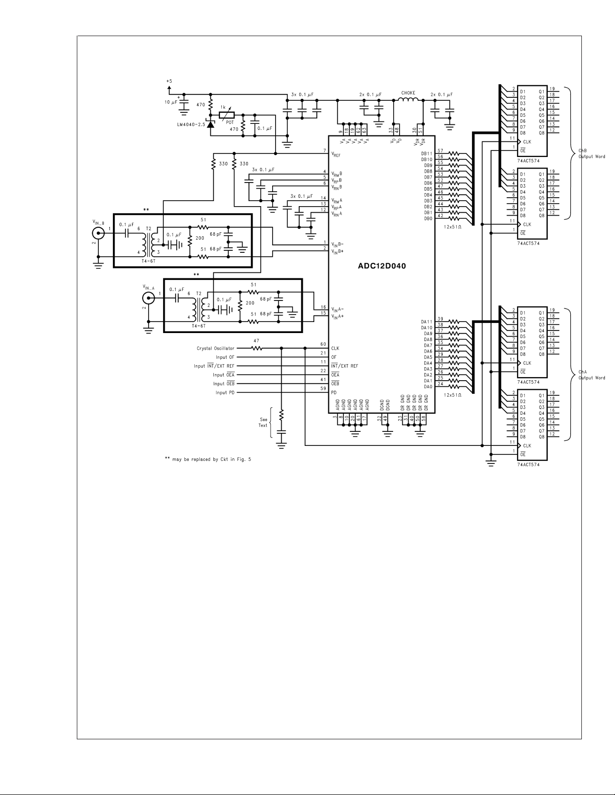
output, use RCs at the inputs, as can be seen in Figure 4
and Figure 5. These components should be placed close to
the ADC inputs because the input pins of the ADC is the
most sensitive part of the system and this is the last opportunity to filter that input.
For Nyquist applications the RC pole should be at the ADC
sample rate. The ADC input capacitance in the sample mode
should be considered when setting the RC pole. Setting the
pole in this manner will provide best SNR performance.
To obtain best SINAD and ENOB performance, reduce the
RC time constant until SNR and THD are numerically equal
to each other. To obtain best distortion and SFDR performance, eliminate the RC altogether.
For undersampling applications, the RC pole should be set
at about 1.15 times the maximum input frequency for narrow
band applications. For wide band applications, the RC pole
should be set at about 1.5 times the maximum input frequency to maintain a linear delay response.
A single-ended to differential conversion circuit is shown in
Figure 5 and Table 3. Resistor Values for Circuit of NS4771
gives resistor values for that circuit to provide input signals in
±
a range of 2.5V
2.0V at each of the differential input pins of
the ADC12D040.
ADC12D040
www.national.com17
Page 18
Applications Information (Continued)
ADC12D040
FIGURE 4. Application Circuit using Transformer or Differential Op-Amp Drive Circuit
www.national.com 18
20046013
Page 19

Applications Information (Continued)
ADC12D040
20046014
FIGURE 5. Differential Drive Circuit of Figure 4
TABLE 3. Resistor Values for Circuit of Figure 5
SIGNAL
RANGE
R1 R2 R3 R4 R5, R6
0 - 0.25V 140Ω 768Ω 226Ω 412Ω 2000Ω
0 - 0.5V 255Ω 768Ω 976Ω 698Ω 1000Ω
0 - 1.0V 464Ω 768Ω 976Ω 137Ω 499Ω
±
0.25V 845Ω 499Ω 845Ω 499Ω 2000Ω
±
0.5V 845Ω 499Ω 845Ω 499Ω 499Ω
1.3.3 Input Common Mode Voltage
The input common mode voltage, V
, should be of a value
CM
such that the peak excursions of the analog signal does not
go more negative than ground or more positive than 1.0
Volts below the V
generally be about V
sources as long as no d.c. current is drawn from these
V
CM
supply voltage. The nominal VCMshould
A
/2. VRMA and VRMB can be used as
REF
pins.
2.0 DIGITAL INPUTS
Digital TTL/CMOS compatible inputs consist of CLK, OEA,
OEB and PD.
2.1 CLK
The CLK signal controls the timing of the sampling process.
Drive the clock input with a stable, low jitter clock signal in
the range of 100 kHz to 55 MHz with rise and fall times of
less than 3ns. The trace carrying the clock signal should be
as short as possible and should not cross any other signal
line, analog or digital, not even at 90˚.
If the CLK is interrupted, or its frequency too low, the charge
on internal capacitors can dissipate to the point where the
accuracy of the output data will degrade. This is what limits
the lowest sample rate to 100 kSPS.
The ADC clock line should be considered to be a transmission line and be series terminated at the source end to match
the source impedance with the characteristic impedance of
the clock line. It generally is not necessary to terminate the
far (ADC) end of the clock line, but if a single clock source is
driving more than one device (a condition that is generally
not recommended), far end termination may be needed. Far
end termination is a series RC with the resistor being the
same as the characteristic impedance of the clock line. The
capacitor should have a minimum value of
20046060
where tPDis the propagation time in ns/unit length, "L" is the
length of the line and Z
the line. The units of t
each other. The typical board of FR-4 material has a t
is the characteristic impedance of
O
and "L" should be consistent with
PD
PD
about 150 ps/inch, or about 60 ps/cm.
The far end termination should be near but beyond the ADC
clock pin as seen from the clock source.
The duty cycle of the clock signal can affect the performance
of any A/D Converter. Because achieving a precise duty
cycle is difficult, the ADC12040 is designed to maintain
performance over a range of duty cycles. While it is specified
and performance is guaranteed with a 50% clock duty cycle,
performance is typically maintained over a clock duty cycle
range of 40% to 60%.
Take care to maintain a constant clock line impedance
throughout the length of the line. Refer to Application Note
AN-905 for information on setting characteristic impedance.
of
www.national.com19
Page 20

Applications Information (Continued)
2.2 OEA, OEB
The OEA or OEB pin, when high, puts the output pins into a
ADC12D040
high impedance state. When this pin is low the outputs are in
the active state. The ADC12D040 will continue to convert
whether this pin is high or low, but the output can not be read
while the pin is high.
Since ADC noise increases with increased output capacitance at the digital output pins, do use the TRI-STATE outputs of the ADC12L066 to drive a bus. Rather, each output
pin should be located close to and drive a single digital input
pin. To further reduce ADC noise, a 100 Ω resistor in series
with each ADC digital output pin, located close to their respective pins, should be added to the circuit.
2.3 PD
The PD pin, when high, holds the ADC12D040 in a powerdown mode to conserve power when the converter is not
being used. The power consumption in this state is 75 mW
with a 40 MHz clock and 40mW if the clock is stopped. The
output data pins are undefined in this mode. The data in the
pipeline is corrupted while in the power down mode.
The Power Down Mode Exit Cycle time is determined by the
value of the capacitors on pins 4, 5, 6, 12, 13 and 14. These
capacitors loose their charge in the Power Down mode and
must be recharged by on-chip circuitry before conversions
can be accurate. Smaller capacitor values allow faster recovery from the power down mode, but can result in a
reduction in SNR, SINAD and ENOB performance.
2.4 OF
The output data format is offset binary when the OF pin is at
a logic low or 2’s complement when the OF pin is at a logic
high. While the sense of this pin may be changed "on the fly,"
doing this is not recommended as the output data could be
erroneous for a few clock cycles after this change is made.
3.0 OUTPUTS
The ADC12D040 has 24 TTL/CMOS compatible Data Output pins. Valid data is present at these outputs while the OE
and PD pins are low. While the tODtime provides information
about output timing, a simple way to capture a valid output is
to latch the data on the falling edge of the conversion clock
(pin 10).
Be very careful when driving a high capacitance bus. The
more capacitance the output drivers must charge for each
conversion, the more instantaneous digital current flows
through V
spikes can cause on-chip ground noise and couple into the
analog circuitry, degrading dynamic performance. Adequate
bypassing, limiting output capacitance and careful attention
to the ground plane will reduce this problem. Additionally,
bus capacitance beyond the specified 20 pF/pin will cause
to increase, making it difficult to properly latch the ADC
t
OD
output data. The result could be an apparent reduction in
dynamic performance.
To minimize noise due to output switching, minimize the load
currents at the digital outputs. This can be done by connecting buffers between the ADC outputs and any other circuitry
(74ACQ541, for example). Only one driven input should be
connected to each output pin. Additionally, inserting series
resistors of 100Ω at the digital outputs, close to the ADC
pins, will isolate the outputs from trace and other circuit
capacitances and limit the output currents, which could otherwise result in performance degradation. See Figure 4.
and DR GND. These large charging current
DR
4.0 POWER SUPPLY CONSIDERATIONS
The power supply pins should be bypassed with a 10 µF
capacitor and with a 0.1 µF ceramic chip capacitor within a
centimeter of each power pin. Leadless chip capacitors are
preferred because they have low series inductance.
As is the case with all high-speed converters, the
ADC12D040 is sensitive to power supply noise. Accordingly,
the noise on the analog supply pin should be kept below 100
.
mV
P-P
No pin should ever have a voltage on it that is in excess of
the supply voltages, not even on a transient basis. Be especially careful of this during turn on and turn off of power.
The V
pin provides power for the output drivers and may
DR
be operated from a supply in the range of 2.35V to V
(nominal 5V). This can simplify interfacing to low voltage
devices and systems. Note, however, that t
reduced V
higher than V
. DO NOT operate the VDRpin at a voltage
DR
.
D
increases with
OD
5.0 LAYOUT AND GROUNDING
Proper grounding and proper routing of all signals are essential to ensure accurate conversion. Maintaining separate
analog and digital areas of the board, with the ADC12D040
between these areas, is required to achieve specified performance.
The ground return for the data outputs (DR GND) carries the
ground current for the output drivers. The output current can
exhibit high transients that could add noise to the conversion
process. To prevent this from happening, the DR GND pins
should NOT be connected to system ground in close proximity to any of the ADC12D040’s other ground pins.
Capacitive coupling between the typically noisy digital circuitry and the sensitive analog circuitry can lead to poor
performance. The solution is to keep the analog circuitry
separated from the digital circuitry, and to keep the clock line
as short as possible.
Digital circuits create substantial supply and ground current
transients. The logic noise thus generated could have significant impact upon system noise performance. The best
logic family to use in systems with A/D converters is one
which employs non-saturating transistor designs, or has low
noise characteristics, such as the 74LS, 74HC(T) and
74AC(T)Q families. The worst noise generators are logic
families that draw the largest supply current transients during clock or signal edges, like the 74F and the 74AC(T)
families.
The effects of the noise generated from the ADC output
switching can be minimized through the use of 100Ω resistors in series with each data output line. Locate these resistors as close to the ADC output pins as possible.
Since digital switching transients are composed largely of
high frequency components, total ground plane copper
weight will have little effect upon the logic-generated noise.
This is because of the skin effect. Total surface area is more
important than is total ground plane volume.
Generally, analog and digital lines should cross each other at
90˚ to avoid crosstalk. To maximize accuracy in high speed,
high resolution systems, however, avoid crossing analog and
digital lines altogether. It is important to keep clock lines as
short as possible and isolated from ALL other lines, including
other digital lines. Even the generally accepted 90˚ crossing
should be avoided with the clock line as even a little coupling
can cause problems at high frequencies. This is because
D
www.national.com 20
Page 21
Applications Information (Continued)
other lines can introduce jitter into the clock line, which can
lead to degradation of SNR. Also, the high speed clock can
introduce noise into the analog chain.
ADC12D040
Best performance at high frequencies and at high resolution
is obtained with a straight signal path. That is, the signal path
through all components should form a straight line wherever
possible.
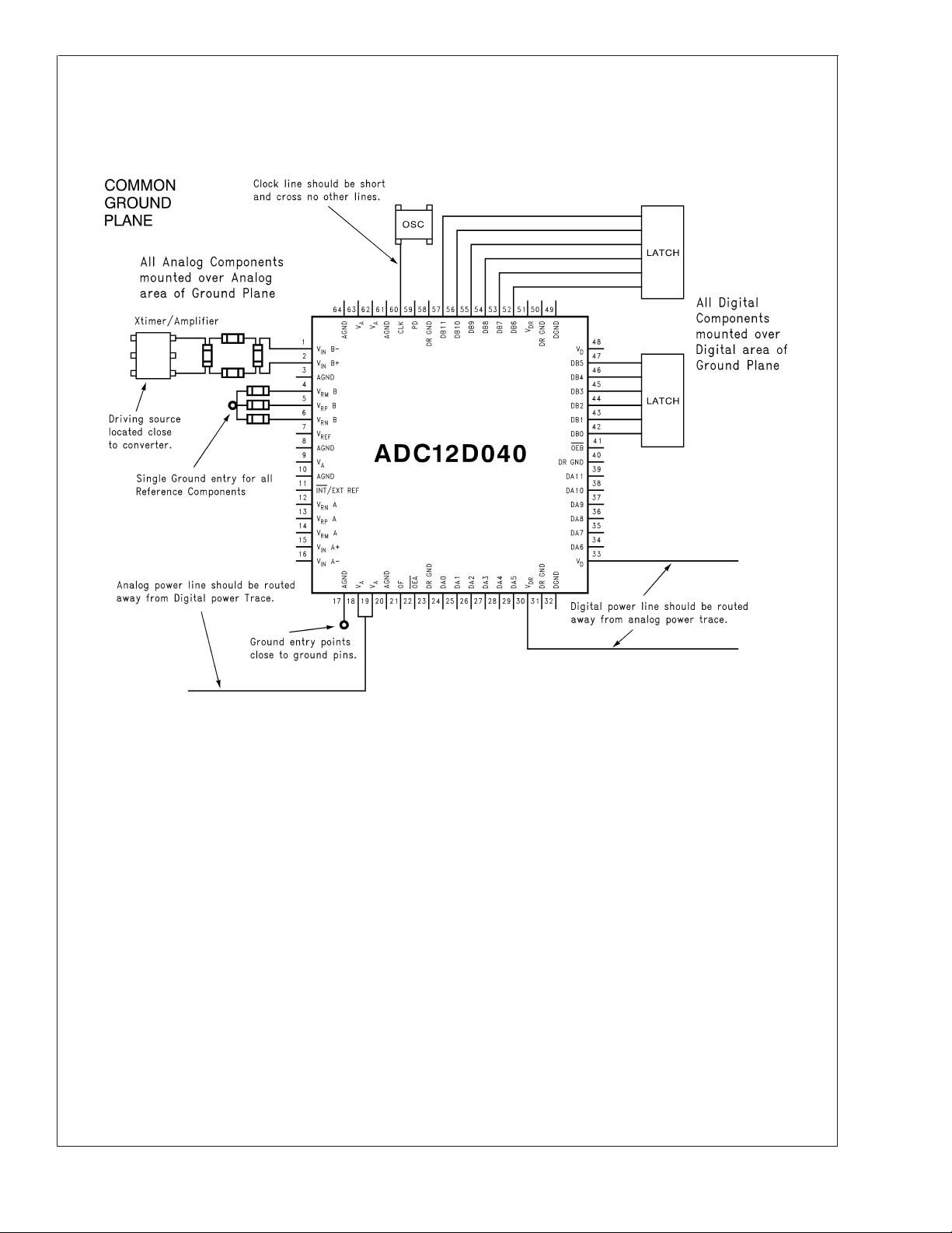
FIGURE 6. Example of a Suitable Layout
Be especially careful with the layout of inductors. Mutual
inductance can change the characteristics of the circuit in
which they are used. Inductors should not be placed side by
side, even with just a small part of their bodies beside each
other.
The analog input should be isolated from noisy signal traces
to avoid coupling of spurious signals into the input. Any
external component (e.g., a filter capacitor) connected between the converter’s input pins and ground or to the reference input pin and ground should be connected to a very
clean point in the analog ground plane.
Figure 6 gives an example of a suitable layout. All analog
circuitry (input amplifiers, filters, reference components, etc.)
should be placed in the analog area of the board. All digital
circuitry and I/O lines should be placed in the digital area of
the board. The ADC12DL066 should be between these two
areas. Furthermore, all components in the reference circuitry
and the input signal chain that are connected to ground
should be connected together with short traces and enter the
analog ground plane at a single, quiet point. All ground
connections should have a low inductance path to ground.
20046016
6.0 DYNAMIC PERFORMANCE
To achieve the best dynamic performance, the clock source
driving the CLK input must be free of jitter. Isolate the ADC
clock from any digital circuitry with buffers, as with the clock
tree shown in Figure 7.
As mentioned in Section 5.0, it is good practice to keep the
ADC clock line as short as possible and to keep it well away
from any other signals. Other signals can introduce jitter into
the clock signal, which can lead to reduced SNR performance, and the clock can introduce noise into other lines.
Even lines with 90˚ crossings have capacitive coupling, so
try to avoid even these 90˚ crossings of the clock line.
www.national.com21
Page 22

Applications Information (Continued)
ADC12D040
FIGURE 7. Isolating the ADC Clock from other Circuitry
with a Clock Tree
7.0 COMMON APPLICATION PITFALLS Driving the inputs (analog or digital) beyond the power
supply rails. For proper operation, all inputs should not go
more than 100 mV beyond the supply rails (more than
100 mV below the ground pins or 100 mV above the supply
pins). Exceeding these limits on even a transient basis may
cause faulty or erratic operation. It is not uncommon for high
speed digital components (e.g., 74F and 74AC devices) to
exhibit overshoot or undershoot that goes above the power
supply or below ground. A resistor of about 50Ω to 100Ω in
series with any offending digital input, close to the signal
source, will eliminate the problem.
Do not allow input voltages to exceed the supply voltage,
even on a transient basis. Not even during power up or
power down.
Be careful not to overdrive the inputs of the ADC12D040 with
a device that is powered from supplies outside the range of
the ADC12D040 supply. Such practice may lead to conversion inaccuracies and even to device damage.
Attempting to drive a high capacitance digital data bus.
The more capacitance the output drivers must charge for
each conversion, the more instantaneous digital current
flows through V
rent spikes can couple into the analog circuitry, degrading
and DR GND. These large charging cur-
DR
20046017
dynamic performance. Adequate bypassing and maintaining
separate analog and digital areas on the pc board will reduce
this problem.
Additionally, bus capacitance beyond the specified 20 pF/pin
will cause t
to increase, making it difficult to properly latch
OD
the ADC output data. The result could, again, be an apparent
reduction in dynamic performance.
The digital data outputs should be buffered (with 74ACQ541,
for example). Dynamic performance can also be improved
by adding series resistors at each digital output, close to the
ADC12D040, which reduces the energy coupled back into
the converter output pins by limiting the output current. A
reasonable value for these resistors is 47Ω to 100Ω.
Using an inadequate amplifier to drive the analog input.
As explained in Section 1.3, the capacitance seen at the
input alternates between 8 pF and 7 pF, depending upon the
phase of the clock. This dynamic load is more difficult to
drive than is a fixed capacitance.
If the amplifier exhibits overshoot, ringing, or any evidence of
instability, even at a very low level, it will degrade performance. A small series resistor at each amplifier output and a
capacitor across the analog inputs (as shown in Figure 5) will
improve performance. The LMH6702 and the LMH6628
have been successfully used to drive the analog inputs of the
ADC12D040.
Also, it is important that the signals at the two inputs have
exactly the same amplitude and be exactly 180
o
out of phase
with each other. Board layout, especially equality of the
length of the two traces to the input pins, will affect the
effective phase between these two signals. Remember that
an operational amplifier operated in the non-inverting configuration will exhibit more time delay than will the same
device operating in the inverting configuration.
Operating with the reference pins outside of the specified range. As mentioned in Section 1.2, V
should be in
REF
the range of
1.0V ≤ V
REF
≤ 2.4V
Operating outside of these limits could lead to performance
degradation.
Using a clock source with excessive jitter, using excessively long clock signal trace, or having other signals
coupled to the clock signal trace. This will cause the
sampling interval to vary, causing excessive output noise
and a reduction in SNR and SINAD performance.
www.national.com 22
Page 23

Physical Dimensions inches (millimeters) unless otherwise noted
ADC12D040 Dual 12-Bit, 40 MSPS, 600 mW A/D Converter with Internal/External Reference
64-Lead TQFP Package
Ordering Number ADC12D040CIVS
NS Package Number VECO64A
LIFE SUPPORT POLICY
NATIONAL’S PRODUCTS ARE NOT AUTHORIZED FOR USE AS CRITICAL COMPONENTS IN LIFE SUPPORT
DEVICES OR SYSTEMS WITHOUT THE EXPRESS WRITTEN APPROVAL OF THE PRESIDENT AND GENERAL
COUNSEL OF NATIONAL SEMICONDUCTOR CORPORATION. As used herein:
1. Life support devices or systems are devices or
systems which, (a) are intended for surgical implant
into the body, or (b) support or sustain life, and
whose failure to perform when properly used in
accordance with instructions for use provided in the
2. A critical component is any component of a life
support device or system whose failure to perform
can be reasonably expected to cause the failure of
the life support device or system, or to affect its
safety or effectiveness.
labeling, can be reasonably expected to result in a
significant injury to the user.
BANNED SUBSTANCE COMPLIANCE
National Semiconductor certifies that the products and packing materials meet the provisions of the Customer Products
Stewardship Specification (CSP-9-111C2) and the Banned Substances and Materials of Interest Specification
(CSP-9-111S2) and contain no ‘‘Banned Substances’’ as defined in CSP-9-111S2.
National Semiconductor
Americas Customer
Support Center
Email: new.feedback@nsc.com
Tel: 1-800-272-9959
www.national.com
National does not assume any responsibility for use of any circuitry described, no circuit patent licenses are implied and National reserves the right at any time without notice to change said circuitry and specifications.
National Semiconductor
Europe Customer Support Center
Fax: +49 (0) 180-530 85 86
Email: europe.support@nsc.com
Deutsch Tel: +49 (0) 69 9508 6208
English Tel: +44 (0) 870 24 0 2171
Français Tel: +33 (0) 1 41 91 8790
National Semiconductor
Asia Pacific Customer
Support Center
Email: ap.support@nsc.com
National Semiconductor
Japan Customer Support Center
Fax: 81-3-5639-7507
Email: jpn.feedback@nsc.com
Tel: 81-3-5639-7560
 Loading...