

Page 1
November 2002
ADC12081
12-Bit, 5 MHz Self-Calibrating, Pipelined A/D Converter
with Internal Sample & Hold
General Description
The ADC12081 is a monolithic CMOS analog-to-digital converter capable of converting analog input signals into 12-bit
digital words at 5 megasamples per second (MSPS). The
ADC12081 utilizes an innovative pipeline architecture to
minimize die size and power consumption. The ADC12081
uses self-calibration and error correction to maintain accuracy and performance over temperature.
The ADC12081 converter operates on a 5V power supply
and can digitize analog input signals in the range of 0 to 2V.
A single convert clock controls the conversion operation. All
digital I/O is TTL compatible.
The ADC12081 is designed to minimize external components necessary for the analog input interface. An internal
sample-and-hold circuit samples the analog input and an
internal amplifier buffers the reference voltage input.
The ADC12081 is available in the 32-lead LQFP package
and is designed to operate over the extended commercial
temperature range of -40˚C to +85˚C.
Features
n Single 5V power supply
n Simple analog input interface
n Internal Sample-and-hold
n Internal Reference buffer amplifier
n Low power consumption
Key Specifications
n Resolution 12 Bits
n Conversion Rate 5 Msps (min)
n DNL
n SNR 68 dB (typ)
n ENOB 10.9 Bits (typ)
n Analog Input Range 2 Vpp (min)
n Supply Voltage +5V
n Power Consumption, 5 MHz 105 mW (typ)
±
0.35 LSB (typ)
Applications
n Image processing front end
n PC-based data acquisition
n Scanners
n Fax machines
n Waveform digitizer
ADC12081 12-Bit, 5 MHz Self-Calibrating, Pipelined A/D Converter with Internal Sample & Hold
±
5%
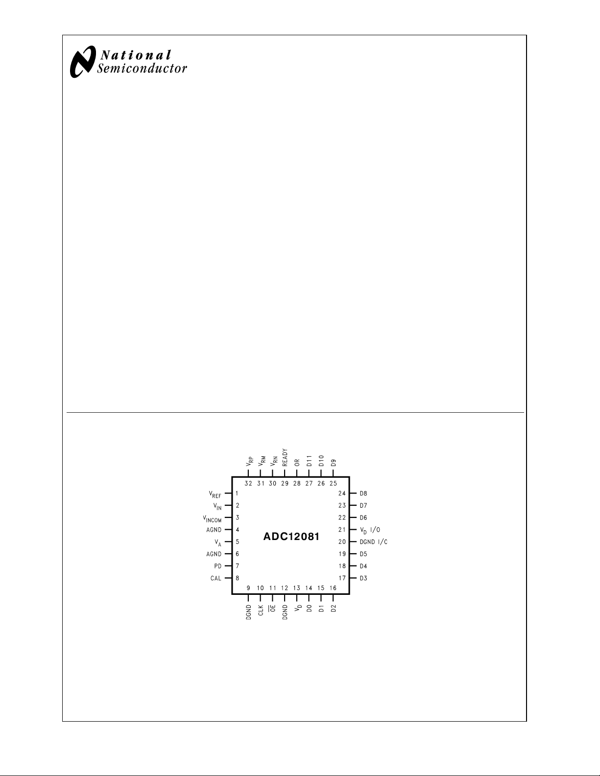
Connection Diagram
10015001
© 2002 National Semiconductor Corporation DS100150 www.national.com
Page 2
Ordering Information
ADC12081
ADC12081CIVT 32 pin LQFP
ADC12181 EVAL Evaluation Board
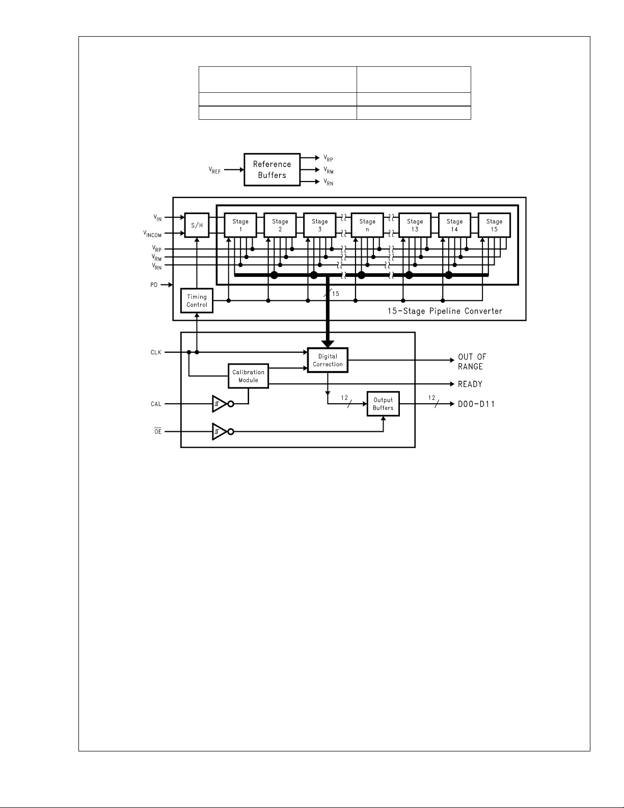
Simplified Block Diagram
Industrial
(−40˚C ≤ TA ≤ +85˚C) Package
10015002
www.national.com 2
Page 3
Pin Descriptions and Equivalent Circuits #2
No. Symbol Equivalent Circuit Description
Analog signal input. With a 2.0V reference voltage,
2V
1V
32 V
31 V
IN
REF
RP
RM
input signal voltages in the range of 0 to 2.0 Volts
will be converted. See section 1.2.
Reference voltage input. This pin should be driven
from an accurate, stable reference source in the
range of 1.8 to 2.2V and bypassed to a low-noise
analog ground with a monolithic ceramic capacitor,
nominally 0.01µF. See section 1.1.
Positive reference bypass pin. Bypass with a 0.1µF
capacitor. Do not connect anything else to this pin.
See section 3.1
Reference midpoint bypass pin. Bypass with a 0.1µF
capacitor. Do not connect anything else to this pin.
See section 3.1
ADC12081
30 V
RN
10 CLOCK
8 CAL
7PD
11 OE
28 OR
29 READY
Negative reverence bypass pin. Bypass with a 0.1µF
capacitor. Do not connect anything else to this pin.
See section 3.1
Sample Clock input, TTL compatible. Maximum
amplitude should not exceed 3V.
Calibration request, active High. Calibration cycle
starts when CAL returns to logic low. CAL is ignored
during power-down mode. See section 2.2.
Power-down, active High, ignored during calibration
cycle. See paragraph 2.4
Output enable control, active low. When this pin is
high the data outputs are in Tri-state
(high-impedance) mode.
Over range indicator. This pin is at a logic High for
V
IN
<
0 or for V
>
V
REF
.
IN
Device ready indicator, active High. This pin is at a
logic Low during a calibration cycle and while the
device is in the power down mode.
www.national.com3
Page 4
Pin Descriptions and Equivalent Circuits #2 (Continued)
ADC12081
No. Symbol Equivalent Circuit Description
14-19,
22-27
3V
5V
4, 6 AGND
13 V
9, 12 DGND
21 V
20 DGND I/O
D0 - D11
IN com
A
D
I/O
D
Digital output word, CMOS compatible. D0 (pin 14) is
LSB, D11 (pin 27) is MSB. Load with no more than
50pF.
Analog input common. Connect to a quiet point in
analog ground near the driving device. See section
1.2.
Positive analog supply pin. Connect to a clean, quiet
voltage source of +5V. V
and VDshould have a
A
common supply and be separately bypassed with a
5µF to 10µF capacitor and a 0.1µF chip capacitor.
The ground return for the analog supply. AGND and
DGND should be connected together close to the
ADC12081 package. See section 5.0.
Positive analog supply pin. Connect to a clean, quiet
voltage source of +5V. V
and VDshould have a
A
common supply and be separately bypassed with a
5µF to 10µF capacitor and a 0.1 µF chip capacitor.
The ground return for the analog supply. AGND and
DGND should be connected together close to the
ADC12081 package. See section 5.0
The digital output driver supply pin. This pin can be
operated from a supply voltage of 3V to 5V, but the
voltage on this pin should never exceed the V
D
supply pin voltage.
The ground return for the output drivers. This pin
should be returned to a point in the digital ground
that is removed from the other ground pins of the
ADC12081.
www.national.com 4
Page 5
ADC12081
Absolute Maximum Ratings (Notes 1,
2)
Storage Temp. −65˚C to +150˚C
Maximum Junction Temp. 150˚C
If Military/Aerospace specified devices are required,
please contact the National Semiconductor Sales Office/
Distributors for availability and specifications.
Supply Voltage 6.5V
Voltage on Any Output −0.3V to V
Input Current at Any Pin (Note 3)
Package Input Current (Note 3)
+
+0.3V
±
25mA
±
50mA
Package Dissipation See (Note 4)
ESD Susceptibility
Operating Ratings
Operating Temp. Range −40˚C ≤ TA≤ +85˚C
Supply Voltage +4.75V to +5.25V
V
I/O +2.7V to V
D
V
Input 1.8V to 2.2V
REF
CLOCK, CAL, PD, OE −0.05V to V
|AGND −DGND| ≤100mV
+ 0.05V
D
Human Body Model 1500V
Machine Model 150V
Soldering Temp., Infrared, 10
300˚C
sec.(Note 6)
Converter Electrical Characteristics
The following specifications apply for AGND = DGND = DGND I/O = 0V, VA=VD=VDI/O = +5V, PD = +5V, V
= 5MHz, CL= 50 pF/pin. After Auto-Cal at Temperature. Boldface limits apply for TA=TJto T
f
CLK
limits T
= 25˚C (Notes 7, 8) and (Note 9)
A=TJ
Symbol Parameter Conditions
Typical
(Note
10)
MIN
Limits
(Note
to T
11)
Static Converter Characteristics
Resolution with No Missing Codes 12 Bits(min)
INL Integral Non Linearity
DNL Differential Non Linearity
Full-Scale Error
Zero Error
±
±
±
±
0.6
0.35
0.05
0.15
±
1.7 LSB( max)
±
0.75 LSB( max)
±
0.1 %FS(max)
±
0.24 %FS(max)
Dynamic Converter Characteristics
BW Full Power Bandwidth 100 MHz
SNR Signal-to-Noise Ratio f
SINAD Signal-to-Noise & Distortion f
ENOB Effective Number of Bits f
THD Total Hamonic Distortion f
SFDR Spurious Free Dynamic Range f
= 2.5 MHz, VIN= 2.0V
in
= 2.5 MHz, VIN= 2.0V
in
= 2.5 MHz, VIN= 2.0V
in
= 2.5 MHz, VIN= 2.0V
in
= 2.5 MHz, VIN= 2.0V
in
P-P
P-P
P-P
P-P
P-P
68 65 dB
67.6 64.5 dB
10.9 10.4 Bits
79 dB
79 dB
Reference and Analog Input Characteristics
V
IN
C
IN
V
REF
Input Voltage Range V
VINInput Capacitance
= 2.0V
REF
V
= 1.0Vdc +
IN
0.7Vrms
(CLK LOW) 10 pF
(CLK HIGH) 15 pF
Reference Voltage (Note 14) 2.00
0
V
REF
1.8 V(min)
2.2 V(max)
Reference Input Leakage Current 10 µA
Reference Input Resistance 1 MΩ(min)
REF
MAX
= +2.0V,
: all other
Units
(Limits)
V(min)
V(max)
D
www.national.com5
Page 6
DC and Logic Electrical Characteristics
The following specifications apply for AGND = DGND = DGND I/O = 0V, VA=VD=VDI/O = +5V, PD = +5V, V
= 50MHz, CL= 50 pF/pin. After Auto-Cal at Temperature. Boldface limits apply for TA=T
f
CLK
ADC12081
T
= 25˚C (Note 7) (Note 8) and (Note 9)
A=TJ
Symbol Parameter Conditions
CLK, OE Digital Input Characteristics
V
IH
V
IL
I
IH
I
IL
C
IN
Logical "1" Input Voltage V+ = 5.25V 2.0 V(min)
Logical "0" Input Voltage V+ = 4.75V 0.8 V(min)
Logical "1" Input Current VIN= 5.0V 5 µA
Logical "0" Input Current VIN=0V −5 µA
VINInput Capacitance 8 pF
D0 - D11 Digital Output Characteristics
V
OH
V
OL
I
OZ
+I
SC
−I
SC
Logical "1" Output Voltage I
Logical "0" Output Voltage I
TRI-STATE®Output Current V
Output Short Circuit Source
Current
= −1mA 4 V (min)
OUT
= 1.6mA 0.4 V (max)
OUT
=3Vor5V 10 µA
OUT
V
= 0V −10 µA
OUT
VDDO= 3V, V
Output Short Circuit Sink Current VDDO= 3V, V
Power Supply Characteristics
I
A
I
D
Analog Supply Current
Digital Supply Current
Total Power Consumption
PD = VDDO
PD = DGND
PD = VDDO
PD = DGND
PD = VDDO
PD = DGND
= 0V −14
OUT
OUT=VO
MIN
Typical
(Note
10)
16 mA(min)
2.5
20
0.5
1
15
105
to T
Limits
; all other limits
MAX
(Note
11)
4
26
2
2
30
140
REF
mA(max)
mA(max)
mA(max)
mA(max)
mW(max)
mW(max)
= +2.0V,
Units
(Limits)
mA(min)
AC Electrical Characteristics
The following specifications apply for AGND = DGND = DGND I/O = 0V, VA=VD=VDI/O = +5V, PD = +5V, V
= 5 MHz, CL= 50 pF/pin. After Auto-Cal at Temperature. Boldface limits apply for TA=T
f
CLK
=TJ= 25˚C (Note 7) (Note 8) and (Note 10)
Symbol Parameter Conditions
f
CLK
Clock Frequency
Clock Duty Cycle 50 %
t
CONV
t
AD
t
OD
t
DIS
t
EN
t
WCAL
t
RDYC
t
CAL
t
WPD
t
RDYPD
t
PD
Conversion Latency 10.25
Aperture Delay Time 3.5 ns
I/O=3V 44
Data output delay after rising clk
edge
V
D
V
I/O=5V 40
D
Data outputs into Tristate mode 21 nA (max)
Data outputs active after Tristate 21 ns (max)
Calibration request pulse width 3 Tclk(min)
Ready Low after CAL request 3 Tclk
Calibration cycle 4000 Tclk
Power-down pulse width 3 Tclk(min)
Ready Low after PD request 3 Tclk
Power down mode exit cycle 4000 Tclk
Typical
(Note
to T
MIN
MAX
Limits
(Note
10)
11)
0.5 MHz(min)
5 MHz(max)
= +2.0V,
REF
; all other limits T
Units
(Limits)
Clock
Cycles
ns
A
www.national.com 6
Page 7

AC Electrical Characteristics (Continued)
Note 1: Absolute Maximum Ratings indicate limits beyond which damage to the device may occur. Operating Ratings indicate conditions for which the device is
functional, but do not guarantee specific performance limits. For guaranteed specifications and test conditions, see the Electrical Characteristics. The guaranteed
specifications apply only for the test conditions listed. Some performance characteristics may degrade when the device is not operated under the listed test
conditions.
Note 2: All voltages are measured with respect to GND = AGND = DGND = 0V, unless otherwise specified.
Note 3: When the input voltage at any pin exceeds the power supplies (that is, V
to 25 mA. The 50 mA maximum package input current rating limits the number of pins that can safely exceed the power supplies with an input current of 25 mA to
two.
Note 4: The absolute maximum junction temperatures (T
junction-to-ambient thermal resistance (θ
TQFP, θ
of this device under normal operation will typically be about 125 mW (typical power consumption + 20 mW TTL output loading). The values for maximum power
consumption listed above will be reached only when the ADC12081 is operated in a severe fault condition (e.g. when input or output pins are driven beyond the
power supply voltages, or the power supply polarity is reversed). Obviously, such conditions should always be avoided.
Note 5: Human body model is 100 pF capacitor discharged through a 1.5kΩ resistor. Machine model is 220 pf discharged through ZERO Ohms.
Note 6: See AN450, "Surface Mounting Methods and Their Effect on Product Reliability", or the section entitled "Surface Mount" found in any post 1986 National
Semiconductor Linear Data Book, for other methods of soldering surface mount devices.
Note 7: The inputs are protected as shown below. Input voltage magnitudes up to 5V above V
is limited per Note 3. However, errors in the A/D conversion can occur if the input goes above V
the full-scale input voltage must be ≤4.85V to ensure accurate conversions.
is 74˚C/W, so PDMAX = 1,689 mW at 25˚C and 1,013 mW at the maximum operating ambient temperature of 75˚C. Note that the power consumption
JA
), and the ambient temperature, (TA), and can be calculated using the formula PDMAX=(TJmax - TA)/θJA. In the 32-pin
JA
max) for this device is 150˚C. The maximum allowable power consumption is dictated by TJmax, the
J
<
IN
AGND, or V
>
VA,VDor VDI/O), the current at that pin should be limited
IN
or to 5V below GND will not damage this device, provided current
A
or below GND by more than 100 mV. As an example, if VAis 4.75V,
A
ADC12081
10015008
Note 8: To guarantee accuracy, it is required that |VA-VD| ≤ 100mV and separate bypassed capacitors are used at each power supply pin.
Note 9: With the test condition for V
Note 10: Typical figures are at T
Note 11: Tested limits are guaranteed to National’s AOQL (Average Outgoing Quality Level).
Note 12: Integral Non Linearity is defined as the deviation of the analog value, expressed in LSBs, from the straight line that passes through positive full-scall and
zero.
Note 13: Timing specifications are tested at the TTL logic levels, V
to 1.4V.
Note 14: Optimum SNR performance will be obtained by keeping the reference input in the 1.8V to 2.2V range. The LM4041CIM3-ADJ (SOT-23 package), the
LM4041CIZ-ADJ (TO-92 package), or the LM4041CIM-ADJ (SOT-8 package) bandgap voltage reference is recommended for this application.
= +2.0V, the 12-bit LSB is 488µV.
REF
= 25˚C, and represent most likely parametric norms.
A=TJ
= 0.4V for a falling edge and VIH= 2.4V for a rising edge. TRI-STATE output voltage is forced
IL
www.national.com7
Page 8

ADC12081
10015009
FIGURE 1. Transfer Characteristic
FIGURE 2. Errors Minimized by the Auto-Cal Cycle
Typical Performance Characteristics
INL vs Temperature DNL vs Temperature
10015011
10015010
10015012
www.national.com 8
Page 9

Typical Performance Characteristics (Continued)
SNR vs Temperature SINAD vs Temperature
10015013 10015014
THD vs Temperature
ADC12081
10015015
www.national.com9
Page 10

Specification Definitions
APERTURE JITTER is the variation in aperture delay from
sample to sample. Aperture jitter shows up as input noise.
ADC12081
APERTURE DELAY See Sampling Delay.
CLOCK DUTY CYCLE is the ratio of the time that the clock
waveform is high to the total time for one clock cycle.
DIFFERENTIAL NON-LINEARITY (DNL) is the measure of
the maximum deviation from the ideal step size of 1 LSB.
EFFECTIVE NUMBER OF BITS (ENOB, or EFFECTIVE
BITS) is another method of specifying Signal-to-Noise and
Distortion Ratio, or SINAD. ENOB is defined as (SINAD -
1.76) / 6.02 and says that the converter is equivalent to a
perfect ADC of this (ENOB) number of bits.
FULL POWER BANDWIDTH is the frequency at which the
reconstructed output fundamental drops 3 dB below its low
frequency value for a full scale input.
FULL SCALE ERROR is the difference between the input
voltage just causing a transition to positive full scale and
-1.5 LSB.
V
REF
INTEGRAL NON-LINEARITY (INL) is a measure of the
deviation of each individual code from a line drawn from
negative full scale (
through positive full scale (1
transition). The deviation of any given code from this straight
line is measured from the center of that code value. The end
point test method is used. INL is commonly measured at
rated clock frequency with a ramp input.
INTERMODULATION DISTORTION (IMD) is the creation of
additional spectral components as a result of two sinusoidal
frequencies being applied to the ADC input at the same time.
It is defined as the ratio of the power in the intermodulation
products to the total power in the original frequencies. IMD is
usually expressed in dB.
1
⁄2LSB below the first code transition)
1
⁄2LSB above the last code
PIPELINE DELAY (LATENCY) is the number of clock cycles
between initiation of conversion and the availability of that
conversion result at the output. New data is available at
every clock cycle, but the data lags the conversion by the
pipeline delay plus the Output Delay.
SAMPLING (APERTURE) DELAY is the time after the edge
of the clock to when the input signal is acquired or held for
conversion.
SIGNAL TO NOISE PLUS DISTORTION (S/(N+D) or SINAD) is the ratio expressed in dB, of the rms value of the
input signal to the rms value of all of the other spectral
components below half the clock frequency, including harmonics but excluding dc.
SIGNAL TO NOISE RATIO (SNR) is the ratio of the rms
value of the input signal to the rms value of the other spectral
components below one-half the sampling frequency, not including harmonics or dc.
SPURIOUS FREE DYNAMIC RANGE (SFDR) is the difference, expressed in dB, between the rms values of the input
signal and the peak spurious signal, where a spurious signal
is any signal present in the output spectrum that is not
present at the input.
TOTAL HARMONIC DISTORTION (THD) is the ratio of the
rms total of the first six harmonic components, to the rms
value of the input signal.
ZERO SCALE OFFSET ERROR is the difference between
the ideal input voltage (
1
⁄2LSB) and the actual input voltage
that just causes a transition from an output code of zero to
an output code of one.
ZERO ERROR see Zero Scale Offset Error.
www.national.com 10
Page 11

Timing Diagrams
ADC12081
FIGURE 3. Data Output Timing
10015021
www.national.com11
Page 12
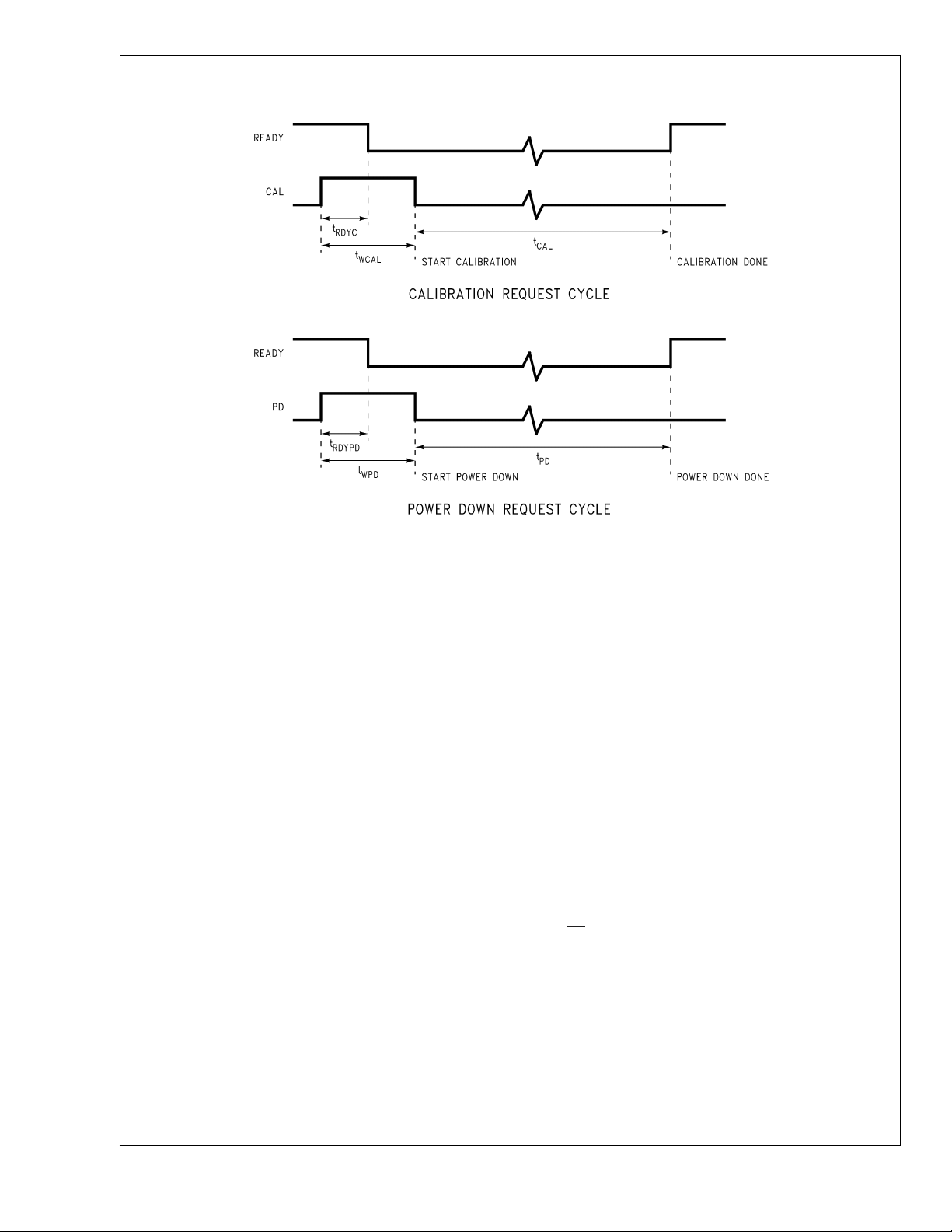
Timing Diagrams (Continued)
ADC12081
10015022
FIGURE 4. Reset and Calibration Timing
Functional Description
The ADC12081 is a monolithic CMOS analog-to-digital converter capable of converting analog input signals into 12-bit
digital words at 5 megasamples per second (MSPS). This
device utilizes a proprietary pipeline architecture and algorithm to minimize die size and power consumption. The
ADC12081 uses self-calibration and digital error correction
to maintain accuracy and performance over temperature.
The ADC12081 has an input sample-and-hold amplifier and
internal reference buffer. The analog input and the reference
voltage are converted to differential signals for internal use.
Using differential signals in the analog conversion core reduces crosstalk and noise pickup from the digital section and
power supply.
The pipeline conversion core has 15 sequential signal processing stages. Each stage receives an analog signal from
the previous stage (called “residue” ) and produces a 1-bit
digital output that is sent to the digital correction module. At
each stage the analog signal received from the previous
stage is compared to an internally generated reference level.
It is then amplified by a factor of 2, and, depending on the
output of the comparator, the internal reference signal may
be subtracted from the amplifier output. This produces the
residue that is passed to the next stage.
The calibration module is activated at power-on or by user
request. During calibration the conversion core is put into a
special mode of operation in order to determine inherent
errors in the analog conversion blocks and to determine
correction coefficients for each digital output bit from the
conversion core and stores these coefficients in RAM. The
digital correction module uses the coefficients in RAM to
convert the raw data bits from the conversion core into the
12-bit digital output code.
Applications Information
1.0 ANALOG INPUTS
The ADC12081 has two single-ended analog inputs. V
the reference input and V
is the signal input.
IN
1.1 Reference Input
The V
input must be driven from an accurate, stable
REF
reference voltage source. of 1.8V to 2.2V, and bypassed to a
clean, quiet point in analog ground.
1.2 Analog Signal Input
The V
input must be driven with a low impedance signal
IN
source that does not add any distortion to the input signal.
The ground reference for the V
V
pin must be connected to a clean, quiet point in
INCOM
input is the V
IN
INCOM
analog ground.
2.0 DIGITAL INPUTS
The ADC12081 has four digital inputs. They are CLOCK,
CAL, OE and PD.
2.1 CLOCK
The CLOCK signal drives an internal phase delay loop to
create timing for the ADC. The clock input should be driven
with a stable, low phase jitter TTL level clock signal in the
range of 0.5 to 5 MHz. The trace carrying the clock signal
should be as short as possible. This trace should not cross
any other signal line, analog or digital, not even at 90˚. A 100
Ohm resistor should be placed in series with the CLOCK pin,
as close to the pin as possible.
REF
pin. The
is
www.national.com 12
Page 13

Applications Information (Continued)
2.2 CAL
The level sensitive CAL input must be pulsed high for at least
three clock cycles to begin ADC calibration. For best performance, calibration should be performed about ten seconds
after power up, after resetting the ADC, and after the temperature has changed by more than 50˚C since the last
calibration was performed.
Calibration should be performed at the same clock frequency that the ADC12081 will be used for conversions to
minimize offset errors. Calibration takes 4000 clock cycles.
Irrelevant data may appear during CAL.
2.3 OE Pin
The OE pin is used to control the state of the outputs. When
the OE pin is low, the output buffers go into the active state.
When the OE input is high, the output buffers are in the high
impedance state.
2.4 PD Pin
The PD pin, when high, holds the ADC12081 in a powerdown mode where power consumption is typically less than
15 mW to conserve power when the converter is not being
used. The ADC12081 will begin normal operation within t
after this pin is brought low, provided a valid CLOCK input is
present. The data in the pipeline is corrupted while in the
power down mode. The ADC12081 should be re-calibrated
after a power-down cycle to ensure optimum performance.
3.0 OUTPUTS
The ADC12081 has three analog outputs: reference output
voltages V
RN,VRM
, and VRP. There are 14 digital outputs:
12 Data Output pins, Ready and OR (Out of range).
3.1 Reference Output Voltages
The reference output voltages are made available only for
the purpose of bypassing with capacitors to a clean analog
ground. The recommended bypass capacitors are 0.1µF
ceramic chip capacitors. Do not load these pins.
3.2 Ready Output
The Ready output goes high to indicate that the converter is
ready for operation. This signal will go low when the converter is Calibration or Power Down made.
PD
3.3 OR (Out of Range) Output
The OR output goes high when the analog input is below
GND or above V
is in the valid range of operation (0V ≤ V
. This output is low when the input signal
REF
≤ V
IN
REF
).
3.4 Data Outputs
The Data Outputs are TTL/CMOS compatible. The output
data format is 12 bits straight binary.
Minimizing the digital output currents will help to minimize
noise due to output switching. This can be done by connecting buffers between the ADC outputs and any other circuitry.
Only one buffer input should be connected to each output.
Additionally, inserting series resistors of 47 to 56 Ohms right
at the digital outputs, close to the ADC pins, will isolate the
outputs from other circuitry and limit output currents.
4.0 POWER SUPPLY CONSIDERATIONS
Each power pin should be bypassed with a parallel combination of a 10µF capacitor and a 0.1µF ceramic chip capacitor. The chip capacitors should be within 1/2 centimeter of
the power pins. Leadless chip capacitors are preferred because they provide low lead inductance.
The converter’s digital logic supply (V
) should be well iso-
D
lated from the supply that is used for other digital circuitry on
the board. A common power supply should be used for both
(analog supply) and VD(digital supply), and each of these
V
A
supply pins should be separately bypassed with a 0.1µF
ceramic capacitor and a low ESR 10µF electrolytic capacitor.
A ferrite bead or inductor should be used between V
and V
A
to prevent noise coupling from the digital supply into the
analog circuit.
I/O is the power pin for the output driver. This pin may be
V
D
supplied with a potential between 2.7V and V
. This makes
D
it easy to interface the ADC12081 with 3V or 5V logic families. Powering the V
I/O from 3 Volts will also reduce power
D
consumption and noise generation due to output switching.
DO NOT operate the V
! All power supplies connected to the device should be
V
A
I/O at a voltage higher than VDor
D
applied simultaneously.
As is the case with all high speed converters, the ADC12081
is sensitive to power supply noise. Accordingly, the noise on
the analog supply pin should be minimized, keeping it below
100mV P-P.
ADC12081
D
www.national.com13
Page 14

Applications Information (Continued)
ADC12081
FIGURE 5. Basic Connections Diagram
5.0 LAYOUT AND GROUNDING
Proper grounding and routing of all signals is essential to
ensure accurate conversion. Separate analog and digital
ground planes that are connected beneath the ADC12081
are required to achieve specified performance. The analog
and digital grounds may be in the same layer, but should be
separated from each other and should never overlap each
other. Separation should be at least 1/8 inch, where possible.
The ground return for the output buffer digital supply (DGND
I/O) carries the ground current for the output drivers. This pin
should be connected to the system digital ground. The current on this pin can exhibit high transients that could add
noise to the conversion process. To prevent this from happening, the DGND I/O pin should NOT be connected in close
proximity to any of the ADC12081’s other ground pins. See .
Capacitive coupling between the typically noisy digital
ground plane and the sensitive analog circuitry can lead to
poor performance that may seem impossible to isolate and
remedy. The solution is to keep the analog circuitry separated from the digital circuitry and from the digital ground
plane.
Digital circuits create substantial supply and ground current
transients. The logic noise thus generated could have significant impact upon system noise performance. The best
10015023
logic family to use in systems with A/D converters is one
which employs non-saturating transistor designs, or has low
noise characteristics, such as the 74LS, 74HC(T) and 74
AC(T)Q families. The worst noise generators are logic families that draw the largest supply current transients during
clock or signal edges, like the 74F and the 74AC(T) families.
Since digital switching transients are composed largely of
high frequency components, total ground plane copper
weight will have little effect upon the logic-generated noise.
This is because of the skin effect. Total surface area is more
important than is total ground plane volume.
An effective way to control ground noise is by connecting the
analog and digital ground planes together beneath the ADC
with a copper trace that is very narrow compared with the
rest of the ground plane. This narrowing beneath the converter provides a fairly high impedance to the high frequency
components of the digital switching currents, directing them
away from the analog pins. The relatively lower frequency
analog ground currents do not create a significant voltage
drop across the impedance of this narrow ground connection.
To maximize accuracy in high speed, high resolution systems, avoid crossing analog and digital signal traces. It is
important to keep any clock lines isolated from ALL other
lines. Even the generally accepted 90 degree crossing
www.national.com 14
Page 15

Applications Information (Continued)
should be avoided as even a little coupling can cause problems at high frequencies. This is because other lines can
introduce phase noise (jitter) into the clock line, which can
lead to degradation of SNR.
Best performance at high frequencies and at high resolution
is obtained with a straight signal path. That is, the signal path
through all components should form a straight line wherever
possible.
Be especially careful with the layout of inductors. Mutual
inductance can change the characteristics of the circuit in
ADC12081
which they are used. Inductors should not be placed side by
side, even with just a small part of their bodies beside each
other.
The analog input should be isolated from noisy signal traces
to avoid coupling of spurious signals into the input. Any
external component (e.g., a filter capacitor) connected between the converter’s input and ground should be connected
to a very clean point in the analog ground plane.
FIGURE 6. Layout example
Figure 6 gives an example of a suitable layout. All analog
circuitry (input amplifiers, filters, reference components, etc.)
should be placed on or over the analog ground plane. All
digital circuitry and I/O lines should be placed over the digital
ground plane.
All ground connections should have a low inductance path to
ground.
6.0 LAYOUT AND GROUNDING
The ADC12081 can achieve impressive dynamic performance. To achieve the best dynamic performance with the
ADC12081, the clock source driving the CLK input must be
free of jitter. For best ac performance, isolating the ADC
clock from any digital circuitry should be done with adequate
buffers, as with a clock tree. See Figure 7.
10015024
10015025
FIGURE 7. Isolating the ADC clock from other circuitry
with a clock tree.
It is good practice to keep the ADC clock line as short as
possible and to keep it well away from any other signals.
Other signals can introduce phase noise (jitter) into the clock
signal, which can lead to increased distortion. Even lines
with 90˚ crossings have capacitive coupling, so try to avoid
even these 90˚ crossings of the clock line.
www.national.com15
Page 16

Applications Information (Continued)
7.0 COMMON APPLICATION PITFALLS Driving the inputs (analog or digital) beyond the power
ADC12081
supply rails. For proper operation, all inputs should not go
more than 300mV beyond the supply rails (more than
300mV below the ground pins or 300mV above the supply
pins). Exceeding these limits on even a transient basis may
cause faulty or erratic operation. It is not uncommon for high
speed digital circuits (e.g., 74F and 74AC devices) to exhibit
undershoot that goes more than a volt below ground above
the power supply. A resistor of about 50 to 100Ω in series
with the offending digital input will eliminate the problem.
Care should be taken not to overdrive the inputs of the
ADC12081 with a device that is powered from supplies
outside the range of the ADC12081 supply. Such practice
may lead to conversion inaccuracies and even to device
damage.
Attempting to drive a high capacitance digital data bus.
Capacitive loading on the digital outputs causes instantaneous digital currents to flow from the V
DGND I/O ground plane. These large charging current
spikes can couple into the analog section, degrading dynamic performance. Adequate bypassing and maintaining
I/O supply into the
D
separate analog and digital ground planes will reduce this
problem. The digital data outputs should be buffered (with
74ACQ541, for example). Dynamic performance can also be
improved by adding series resistors at each digital output,
close to the ADC12081, reducing the energy coupled back
into the converter output pins by limiting the output slew rate.
A reasonable value for these resistors is 47Ω.
Using an inadequate amplifier to drive the analog input.
The analog input circuits of the ADC12081 place a switched
capacitor load on the input signal source. Therefore the
amplifier used to drive the ADC12081 must have a low
impedance output and adequate bandwidth to avoid distortion of the input signal.
Operating with the reference pins outside of the specified range. As mentioned in section 1.1, V
the range of 1.8V ≤ V
≤ 2.2V. Operating outside of these
REF
should be in
REF
limits could lead to signal distortion.
Using a clock source with excessive jitter, using excessively long clock signal trace, or having other signals
coupled to the clock signal trace. This will cause the
sampling interval to vary, causing excessive output noise
and a reduction in SNR performance.
www.national.com 16
Page 17

Physical Dimensions inches (millimeters)
unless otherwise noted
ADC12081 12-Bit, 5 MHz Self-Calibrating, Pipelined A/D Converter with Internal Sample & Hold
32-Lead LQFP Package
Ordering Number ADC12081CIVT
NS Package Number VBE32A
LIFE SUPPORT POLICY
NATIONAL’S PRODUCTS ARE NOT AUTHORIZED FOR USE AS CRITICAL COMPONENTS IN LIFE SUPPORT
DEVICES OR SYSTEMS WITHOUT THE EXPRESS WRITTEN APPROVAL OF THE PRESIDENT AND GENERAL
COUNSEL OF NATIONAL SEMICONDUCTOR CORPORATION. As used herein:
1. Life support devices or systems are devices or
systems which, (a) are intended for surgical implant
into the body, or (b) support or sustain life, and
whose failure to perform when properly used in
accordance with instructions for use provided in the
2. A critical component is any component of a life
support device or system whose failure to perform
can be reasonably expected to cause the failure of
the life support device or system, or to affect its
safety or effectiveness.
labeling, can be reasonably expected to result in a
significant injury to the user.
National Semiconductor
Corporation
Americas
Email: support@nsc.com
www.national.com
National Semiconductor
Europe
Fax: +49 (0) 180-530 85 86
Email: europe.support@nsc.com
Deutsch Tel: +49 (0) 69 9508 6208
English Tel: +44 (0) 870 24 0 2171
Français Tel: +33 (0) 1 41 91 8790
National Semiconductor
Asia Pacific Customer
Response Group
Tel: 65-2544466
Fax: 65-2504466
Email: ap.support@nsc.com
National Semiconductor
Japan Ltd.
Tel: 81-3-5639-7560
Fax: 81-3-5639-7507
National does not assume any responsibility for use of any circuitry described, no circuit patent licenses are implied and National reserves the right at any time without notice to change said circuitry and specifications.
 Loading...