

Page 1
ADC12041
12-Bit Plus Sign 216 kHz Sampling
Analog-to-Digital Converter
ADC12041 12-Bit Plus Sign 216 kHz Sampling Analog-to-Digital Converter
December 1995
General Description
Operating from a single 5V power supply the ADC12041 is a
a
12 bit
sign, parallel I/O, self-calibrating, sampling analogto-digital converter (ADC). The maximum sampling rate is
216 kHz. On request, the ADC goes through a self-calibration process that adjusts linearity, zero and full-scale errors.
The ADC12041 can be configured to work with many popular microprocessors/microcontrollers including National’s
HPC family, Intel386 and 8051, TMS320C25, Motorola
MC68HC11/16, Hitachi 64180 and Analog Devices
ADSP21xx.
For complementary voltage references see the LM4040,
LM4041 or LM9140.
Key Specifications (f
Y
Resolution 12-bitsasign
Y
13-bit conversion time 3.6 ms, max
Y
13-bit throughput rate 216 ksamples/s, min
Y
Integral Linearity Error (ILE)
Y
Single supply
CLK
e
12 MHz)
g
1 LSB, max
a
5Vg10%
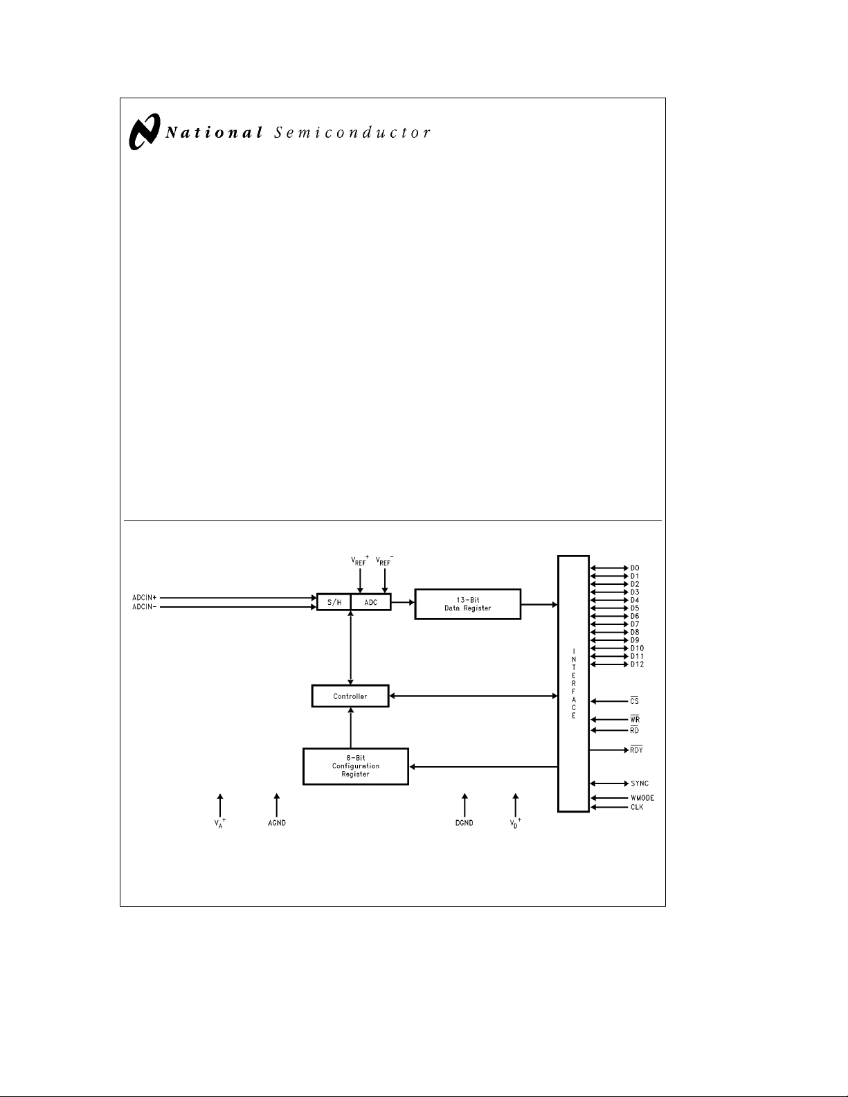
Block Diagram
Y
VINrange GND to V
Y
Power consumption:
Normal operation 33 mW, max
Stand-by mode 75 mw, max
Features
Y
Fully differential analog input
Y
Programmable acquisition times and user-controllable
throughput rates
Y
Programmable data bus width (8/13 bits)
Y
Built-in Sample-and-Hold
Y
Programmable auto-calibration and auto-zero cycles
Y
Low power standby mode
Y
No missing codes
Applications
Y
Medical instrumentation
Y
Process control systems
Y
Test equipment
Y
Data logging
Y
Inertial guidance
a
A
TL/H/12441– 1
TRI-STATEÉis a registered trademark of National Semiconductor Corporations.
C
1996 National Semiconductor Corporation RRD-B30M26/Printed in U. S. A.
TL/H/12441
Page 2
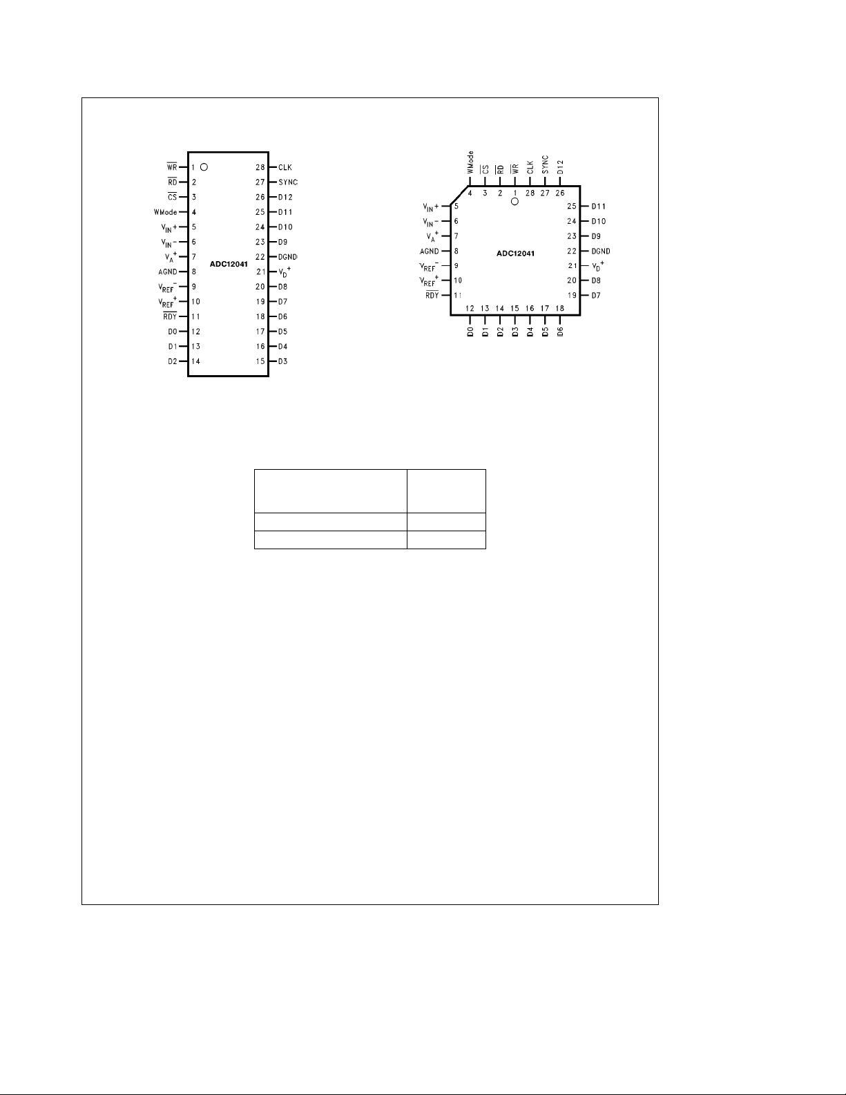
Connection Diagrams
28-Pin SSOP
28-Pin PLCC
Order Number ADC12041CIMSA
See NS Package Number MSA28
Ordering Information
Order Number ADC12041CIV
See NS Package Number V28A
TL/H/12441– 2
Industrial Temperature Range
b
40§CsT
ADC12041CIV V28A
ADC12041CIMSA MSA28, SSOP
s
a
85§C
A
NS
Package
Number
TL/H/12441– 3
2
Page 3
Absolute Maximum Ratings
(Notes 1 and 2)
Supply Voltage (V
Voltage at all Inputs
ab
V
l
A
AGNDbDGND
l
Input Current at Any Pin (Note 3)
Package Input Current (Note 3)
Power Dissipation (Note 4)
e
at T
A
Storage Temperature
Lead Temperature
SSOP Package
Vapor Phase (60 sec.) 210
Infared (15 sec.) 220
V Package, Infared (15 sec.) 300
a
A
a
V
l
D
a
and V
) 6.0V
D
b
0.3V to V
a
l
g
25§C 500 mW
b
65§Ctoa150§C
a
0.3V
300 mV
300 mV
g
30 mA
120 mA
§
§
§
Operating Ratings (Notes 1 and 2)
Temperature Range
s
(T
Supply Voltage
V
A
a
V
l
A
AGNDbDGND
l
VINVoltage Range at all Inputs GNDsV
V
REF
V
REF
V
REF
V
REF
C
C
C
s
T
T
min
a
a
,V
D
a
b
V
D
)
A
max
l
l
a
Input Voltage 1VsV
b
Input Voltage 0sV
a
Common Mode 0.1 V
b
b
V
REF
a
A
ESD Susceptibility (Note 5) 3.0 kV
Converter DC Characteristics The following specifications apply to the ADC12041 for V
a
e
V
and V
otherwise specified. Boldface limits apply for T
REF
4.096V, V
b
s
1X, fully differential input with fixed 2.048V common-mode voltage (V
REF
Symbol Parameter Conditions
b
e
0.0V, 12-bitasign conversion mode, f
REF
e
12.0 MHz, R
CLK
e
e
T
T
A
J
MIN
to T
MAX
e
25X, source impedance for V
S
), and minimum acquisition time, unless
INCM
; all other limits T
e
T
A
Typical Limits Units
(Note 10) (Note 11) (Limit)
Resolution with No Missing Codes After Auto-Cal 13 Bits (max)
ILE Positive and Negative Integral After Auto-Cal
Linearity Error (Notes 12 and 17)
g
0.6
DNL Differential Non-Linearity After Auto-Cal
Zero Error After Auto-Cal (Notes 13 and 17)
e
V
V
V
Positive Full-Scale Error After Auto-Cal (Notes 12 and 17)
Negative Full-Scale Error After Auto-Cal (Notes 12 and 17)
DC Common Mode Error After Auto-Cal (Note 14)
TUE Total Unadjusted Error After Auto-Cal (Note 18)
INCM
INCM
INCM
e
e
5.0V
2.048V
0V
g
1.0
g
1.0
g
2
g
1 LSB
b
40§CsT
s
A
4.5V to 5.5V
s
100 mV
s
100 mV
a
s
IN
a
s
REF
b
REF
1VsV
s
V
REFCM
A
e
25§C
J
g
1 LSB (max)
g
1 LSB (max)
g
5.5
g
2.0
g
5.5
g
2.5 LSB (max)
g
2.5 LSB (max)
g
5.5 LSB (max)
a
s
V
REF
s
REF
s
0.6 V
a
a
e
V
D
LSB (max)
b
e
REF
85§C
V
A
V
A
1V
V
A
A
5V,
a
a
a
a
a
3
Page 4
Power Supply Characteristics The following specifications apply to the ADC12041 for V
a
e
V
and V
specified. Boldface limits apply for T
REF
4.096V, V
b
1X, fully differential input with fixed 2.048V common-mode voltage, and minimum acquisition time, unless otherwise
REF
Symbol Parameter Conditions
PSS Power Supply Sensitivity V
Zero Error V
Full-Scale Error V
Linearity Error
a
I
D
a
V
Digital Supply Current Start Command (Performing a conversion) with SYNC
D
b
e
0.0V, 12-bitasign conversion mode, f
REF
e
T
A
a
e
V
D
a
e
REF
b
e
REF
configured as an input and driven with a 214 kHz
e
J
a
A
4.096V
0V
T
to T
MIN
e
5.0Vg10%
CLK
; all other limits T
MAX
e
12.0 MHz, R
e
25X, source impedance for V
S
e
e
T
A
25§C
J
Typical Limits Unit
(Note 10) (Note 11) (Limit)
g
0.1 LSB
g
0.5 LSB
g
0.1 LSB
signal. Bus width set to 13.
e
f
12.0 MHz, Reset Mode 850 mA
CLK
e
f
12.0 MHz, Conversion 2.45 2.6 mA (max)
a
I
A
a
V
Analog Supply Current Start Command (Performing a conversion) with SYNC
A
CLK
configured as an input and driven with a 214 kHz
signal. Bus width set to 13.
e
f
12.0 MHz, Reset Mode 2.3 mA
CLK
e
f
12.0 MHz, Conversion 2.3 4.0 mA (max)
CLK
I
ST
Symbol Parameter Conditions
I
IN
R
CV
Standby Supply Current Standby Mode
a
a
a
(I
I
D
Analog Input Characteristics The following specifications apply to the ADC12041 for V
a
e
V
REF
a
V
and V
REF
otherwise specified. Boldface limits apply for T
)f
A
b
4.096V, V
a
REF
e
REF
s
0.0V, 12-Bitasign conversion mode, f
1X, fully differential input with fixed 2.048V common-mode voltage, and minimum acquisition time, unless
e
Stopped 5 15 mA (max)
CLK
e
f
12.0 MHz 100 120 mA (max)
CLK
e
12.0 MHz, R
CLK
e
e
T
T
to T
A
J
MIN
; all other limits T
MAX
e
25X, source impedance for
S
Typical Limits Unit
(Note 10) (Note 11) (Limit)
a
V
IN
ADC Input On Resistance V
ON
ADC Input Capacitance 10 pF
IN
and V
b
Input Leakage Current V
IN
a
e
5V 0.05
IN
b
e
V
0V
IN
e
2.5V
IN
Refer to section titled INPUT CURRENT.
b
0.05
1000 X
a
A
a
A
e
T
A
J
2.0 mA (max)
e
e
e
V
D
V
D
25§C
a
e
5V,
a
REF
a
e
5V,
a
a
e
Reference Inputs The following specifications apply to the ADC12041 for V
b
e
V
1X, fully differential input with fixed 2.048V common-mode voltage, and minimum acquisition time, unless otherwise specified.
Boldface limits apply for T
0.0V, 12-bitasign conversion mode, f
REF
e
e
T
A
T
J
MIN
CLK
to T
e
MAX
12.0 MHz, R
S
; all other limits T
e
25X, source impedance for V
e
T
A
Symbol Parameter Conditions
I
REF
Reference Input Current V
a
4.096V, V
REF
Analog Input Signal: 1 kHz 145 mA
REF
b
e
0V
e
V
A
e
25§C
J
5V, V
D
Typical Limits Unit
(Note 10) (Note 11) (Limit)
REF
REF
a
a
and V
e
4.096V,
b
REF
(Note 20) 80 kHz 136 mA
C
REF
Reference Input Capacitance 85 pF
4
s
Page 5
Digital Logic Input/Output Characteristics The following specifications apply to the ADC12041 for
a
a
e
V
A
impedance for V
tion time, unless otherwise specified. Boldface limits apply for T
e
V
D
REF
25§C
Symbol Parameter Conditions
V
IH
V
IL
I
IH
I
IL
V
OH
V
OL
I
OFF
C
IN
Converter AC Characteristics The following specifications apply to the ADC12041 for V
V
REF
and V
otherwise specified. Boldface limits apply for T
Logic High Input Voltage V
Logic Low Input Voltage V
Logic High Input Current V
Logic Low Input Current V
Logic High Output Voltage V
Logic Low Output Voltage V
TRI-STATE Output Leakage Current V
D12–D0 Input Capacitance 10 pF
a
e
4.096V, V
b
s
REF
1X, fully differential input with fixed 2.048V common-mode voltage, and minimum acquisition time, unless
Symbol Parameter Conditions
t
Z
t
CAL
5V, V
a
REF
and V
a
e
4.096V, V
b
REF
s
b
1X, fully differential input with fixed 2.048V common-mode voltage, and minimum acquisi-
e
e
T
A
T
J
MIN
e
0.0V, 12-bitasign conversion mode, f
REF
CLK
to T
e
12.0 MHz, R
; all other limits T
MAX
e
S
25X, source
e
A
Typical Limits Unit
(Note 10) (Note 11) (Limit)
a
a
e
e
V
5.5V 2.2 V (min)
D
a
e
V
4.5V 0.8 V (max)
D
a
V
D
1.6 mA
V
D
1.6 mA
0V
5V
CLK
T
MIN
e
a
e
to T
4.5V
4.5V
e
12.0 MHz, R
MAX
b
0.035
2.4 2.4 V (min)
0.4 0.4 V (max)
e
25X, source impedance for V
S
; all other limits T
b
g
e
T
A
J
2.0 mA (max)
2.0 mA (max)
a
a
e
V
S
D
e
25§C
b
e
0.0V, 12-bitasign conversion mode, f
REF
A
a
e
A
e
5V 0.035 2.0 mA (max)
IN
e
0V
IN
ae
A
eb
I
OUT
a
e
A
e
I
OUT
e
OUT
e
V
OUT
e
e
T
A
J
Typical Limits Unit
(Note 10) (Note 11) (Limit)
Auto Zero Time 78 78 clksa120 ns clks (max)
Full Calibration Time 4946 4946 clksa120 ns clks (max)
e
REF
T
J
5V,
CLK Duty Cycle 50 %
40 % (min)
60 % (max)
t
CONV
t
AcqSYNCOUT
Conversion Time Sync-Out Mode 44 44 clks (max)
Acquisition Time Minimum for 13 Bits 9 9 clksa120 ns clks (max)
(Programmable) Maximum for 13 Bits 79 79 clks
a
120 ns clks (max)
e
a
5
Page 6
Digital Timing Characteristics The following specifications apply to the ADC12041, 13-bit data bus width,
a
a
e
V
A
Symbol
(Figure 7)
t
TPR
e
V
D
Throughput Rate Sync-Out Mode (SYNC Bite‘‘0’’) 222 kHz
5V, f
CLK
e
12 MHz, t
e
f
3 ns and C
e
50 pF on data I/O lines
L
Parameter Conditions
9 Clock Cycles of Acquisition
Typical Limits Unit
(Note 10) (Note 11) (Limit)
Time
t
CSWR
t
WRCS
t
WR
t
WRSETFalling
t
WRHOLDFalling
t
WRSETRising
t
WRHOLDRising
t
CSRD
t
RDCS
t
RDDATA
t
RDDATA
t
RDHOLD
t
RDRDY
t
WRRDY
t
STDRDY
Falling Edge of CS
to Falling Edge of WR
Active Edge of WR
to Rising Edge of CS
0ns
0ns
WR Pulse Width 20 30 ns (min)
Write Setup Time WMODEe‘‘1’’ 20 ns (min)
Write Hold Time WMODEe‘‘1’’ 5 ns (min)
Write Setup Time WMODEe‘‘0’’ 20 ns (min)
Write Hold Time WMODEe‘‘0’’ 5 ns (min)
Falling Edge of CS
to Falling Edge of RD
Rising Edge of RD
to Rising Edge of CS
0ns
0ns
Falling Edge of RD to Valid Data 8-Bit Mode (BW Bite‘‘0’’) 40 58 ns (max)
Falling Edge of RD to Valid Data 13-Bit Mode (BW Bite‘‘1’’) 26 44 ns (max)
Read Hold Time 23 32 ns (max)
Rising Edge of RD
to Rising Edge of RDY
Active Edge of WR WMODEe‘‘1’’
to Rising Edge of RDY
24 38 ns (max)
37 60 ns (max)
Active Edge of WR WMODEe‘‘0’’. Writing the
to Falling Edge of RDY
RESET Command into the
1.4 2.5 ms (max)
Configuration Register
t
SYNC
Minimum SYNC Pulse Width 5 10 ns (min)
Notes on Specifications
Note 1: Absolute Maximum Ratings indicate limits beyond which damage to the device may occur. Operating Ratings indicate conditions for which the device is
functional, but do not guarantee specific performance limits. For guaranteed specifications and test conditions, see the Electrical Characteristics. The guaranteed
specifications apply only for the test conditions listed. Some performance characteristics may degrade when the device is not operated under the listed test
conditions.
Note 2: All voltages are measured with respect to GND, unless otherwise specified.
Note 3: When the input voltage (V
mA. The 120 mA maximum package input current limits the number of pins that can safely exceed the power supplies with an input current of 30 mA to four.
Note 4: The maximum power dissipation must he derated at elevated temperatures and is dictated by T
junction to ambient thermal resistance), and T
or the number given in the Absolute Maximum Ratings, whichever is lower. For this device, T
i
JA
ADC12041 in the V package, when board mounted, is 55
Note 5: Human body model, 100 pF discharged through 1.5 Xk resistor.
) at any pin exceeds the power supply rails (V
IN
(ambient temperature). The maximum allowable power dissipation at any temperature is P
A
C/W, and in the SSOP package, when board mounted, is 130§C/W.
§
IN
k
GND or V
6
a
l
IN
Jmax
a
(V
or V
)), the current at that pin should be limited to 30
A
D
, (maximum junction temperature), iJA(package
Jmax
e
150§C, and the typical thermal resistance (iJA)ofthe
Dmax
e
b
(T
TA)/
Jmax
Page 7
Notes on Specifications (Continued)
Note 6: Each input is protected by a nominal 6.5V breakdown voltage zener diode to GND, as shown below, input voltage magnitude up to 5V above V
below GND will not damage the ADC12041. There are parasitic diodes that exist between the inputs and the power supply rails and errors in the A/D conversion
can occur if these diodes are forward biased by more than 50 mV. As an example, if V
conversions.
a
is 4.50 VDC, full-scale input voltage must be 4.55 VDCto ensure accurate
A
a
or 5V
A
a
A
TL/H/12441– 4
a
and V
at the specified extremes.
D
a
Note 7: V
conversion/comparison accuracy. Refer to the Power Supply Considerations section for a detailed discussion.
Note 8: Accuracy is guaranteed when operating at f
Note 9: With the test condition for V
Note 10: Typicals are at T
Note 11: Limits are guaranteed to National’s AOQL (Average Outgoing Quality Level).
Note 12: Positive integral linearity error is defined as the deviation of the analog value, expressed in LSBs, from the straight line that passes through positive full-
scale and zero. For negative integral linearity error, the straight line passes through negative full-scale and zero.
Note 13: Zero error is a measure of the deviation from the mid-scale voltage (a code of zero), expressed in LSB. It is the average value of the code transitions
b
between
Note 14: The DC common-mode error is measured with both inputs shorted together and driven from 0V to 5V. The measured value is referred to the resulting
output value when the inputs are driven with a 2.5V input.
Note 15: Power Supply Sensitivity is measured after an Auto-Zero and Auto Calibration cycle has been completed with V
Note 16: V
Note 17: The ADC12041’s self-calibration technique ensures linearity and offset errors as specified, but noise inherent in the self-calibration process will result in a
repeatability uncertainty of
a
and V
A
1to0and0toa1 (see
REFCM
must be connected together to the same power supply voltage and bypassed with separate capacitors at each Vapin to assure
D
CLK
a
b
REF(VREF
e
25§C and represent most likely parametric norm.
A
Figure 6
V
REF
).
(Reference Voltage Common Mode Range) is defined as
g
0.20 LSB.
e
12 MHz.
b
) given asa4.096V, the 12-bit LSB is 1.000 mV.
a
b
a
V
V
REF
REF
2
#
J
Note 18: Total Unadjusted Error (TUE) includes offset, full scale linearity and MUX errors.
Note 19: The ADC12041 parts used to gather the information for these curves were auto-calibrated prior to taking the measurements at each test condition. The
auto-calibration cycle cancels any first order drifts due to test conditions. However, each measurement has a repeatability uncertainty error of 0.2 LSB. See Note
17.
Note 20: This is a DC average current drawn by the reference input with a full-scale sinewave input. The ADC12041 is continuously converting with a throughput
rate of 206 kHz.
Note 21: These typical curves were measured during continuous conversions with a positive half-scale DC input. A 240 ns RD
signal went low. The data bus lines were loaded with 2 HC family CMOS inputs (C
RDY
Note 22: Any other values placed in the command field are meaningless. However, if a code of 101 or 110 is placed in the command field and the CS
go low at the same time, the ADC12041 will enter a test mode. These test modes are only to be used by the manufacturer of this device. A hardware power-off and
power-on reset must be done to get out of these test modes.
E
20 pF).
L
pulse was applied 25 ns after the
,RDand WR
7
Page 8
Electrical Characteristics
FIGURE 1. Output Digital Code vs the Operating Input Voltage Range (General Case)
FIGURE 2. Output Digital Code vs the Operating Input Voltage Range for V
REF
e
TL/H/12441– 5
TL/H/12441– 6
4.096V
8
Page 9
Electrical Characteristics (Continued)
FIGURE 3. V
FIGURE 4. V
Operating Range (General Case)
REF
Operating Range for V
REF
TL/H/12441– 7
e
5V
A
TL/H/12441– 8
9
Page 10

Electrical Characteristics (Continued)
FIGURE 5a. Transfer Characteristic
FIGURE 5b. Simplified Error vs Output Code without Auto-Calibration or Auto-Zero Cycles
TL/H/12441– 9
TL/H/12441– 10
10
Page 11

Electrical Characteristics (Continued)
FIGURE 5c. Simplified Error vs Output Code after Auto-Calibration Cycle
TL/H/12441– 12
FIGURE 6. Offset or Zero Error Voltage (Note 13)
TL/H/12441– 11
11
Page 12

Timing Diagrams
FIGURE 7a. Sync-Out Write (WMODEe1, BWe1), Read and Convert Cycles
FIGURE 7b. Sync-In Write (WMODEe1, BWe1), Read and Convert Cycles
TL/H/12441– 13
TL/H/12441– 14
12
Page 13

Timing Diagrams (Continued)
FIGURE 7c. Sync-Out Write (WMODEe0, BWe1), Read and Convert Cycles
FIGURE 7d. Sync-In Write (WMODEe0, BWe1), Read and Convert Cycles
TL/H/12441– 46
TL/H/12441– 47
13
Page 14

Timing Diagrams (Continued)
FIGURE 7e. Sync-Out Read and Convert Cycles
FIGURE 7f. Sync-In Read and Convert Cycles
TL/H/12441– 48
TL/H/12441– 49
14
Page 15

Timing Diagrams (Continued)
FIGURE 7g. 8-bit Bus Read Cycle (Sync-Out)
FIGURE 7h. 8-bit Bus Read Cycle (Sync-In)
15
TL/H/12441– 50
TL/H/12441– 51
Page 16

Timing Diagrams (Continued)
FIGURE 7i. Write Signal Negates RDY (Writing the Standby, Auto-Cal or Auto-Zero Command)
FIGURE 7j. Standby and Reset Timing (13-Bit Data Bus Width)
TL/H/12441– 15
TL/H/12441– 16
16
Page 17

Typical Performance Characteristics (See Note 19, Electrical Characteristic Section)
Integral Linearity Error (INL)
Change vs Clock Frequency
TL/H/12441– 17
Integral Linearity Error (INL)
Change vs Temperature
TL/H/12441– 20
Integral Linearity Error (INL)
Change vs Reference Voltage
Full-Scale Error Change vs
Clock Frequency
TL/H/12441– 18
Full-Scale Error Change vs
Temperature
TL/H/12441– 21
Full-Scale Error Change vs
Reference Voltage
Zero Error Change vs
Clock Frequency
TL/H/12441– 19
Zero Error Change vs
Temperature
TL/H/12441– 22
Zero Error Change vs
Reference Voltage
TL/H/12441– 23
Integral Linearity Error (INL)
Change vs Supply Voltage
TL/H/12441– 26
TL/H/12441– 24
Full-Scale Error Change
vs Supply Voltage
TL/H/12441– 27
17
TL/H/12441– 25
Zero Error Change
vs Supply Voltage
TL/H/12441– 28
Page 18

Typical Performance Characteristics (See Note 21, Electrical Characteristic Section) (Continued)
Supply Current vs
Clock Frequency
Analog Supply Current
vs Temperature
TL/H/12441– 29
TL/H/12441– 31
Reference Current vs
Clock Frequency
TL/H/12441– 30
Digital Supply Current vs
Temperature
TL/H/12441– 32
18
Page 19

Typical Performance Characteristics (Continued) The curves were obtained under the following condi-
e
tions. R
S
otherwise stated.
50X,T
e
A
25§C, V
a
a
e
e
V
A
5V, V
D
REF
e
4.096V, f
e
12 MHz, and the sampling rate f
CLK
e
215 kHz unless
S
Full Scale Differential 1,099 Hz
Sine Wave Input
Full Scale Differential 38,452 Hz
Sine Wave Input
Half Scale Differential 1 kHz
Sine Wave Input, f
e
S
153.6 kHz
TL/H/12441– 33
TL/H/12441– 35
Full Scale Differential 18,677 Hz
Sine Wave Input
Full Scale Differential 79,468 Hz
Sine Wave Input
Half Scale Differential 20 kHz
Sine Wave Input, f
e
S
153.6 kHz
TL/H/12441– 34
TL/H/12441– 36
Half Scale Differential 40 kHz
Sine Wave Input, f
e
S
153.6 kHz
TL/H/12441– 37
TL/H/12441– 39
TL/H/12441– 38
Half Scale Differential 75 kHz
Sine Wave Input, f
e
S
153.6 kHz
TL/H/12441– 40
19
Page 20

Pin Description
PLCC and
SSOP Pkg.
Pin Number
5V
6V
10 V
9V
4 WMODE The logic state of this pin at power-up determines which edge of the write signal (WR) will latch in data
27 SYNC The SYNC pin can be programmed as an input or an output. The Configuration register’s bit b4 controls
12–20 D0 –D8 13-bit Data bus of the ADC12041. D12 is the most significant bit and D0 is the least significant. The
23–26 D9 –D12 BW(bus width) bit of the Configuration register (b3) selects between an 8-bit or 13-bit data bus width.
28 CLK The clock input pin used to drive the ADC12041. The operating range is 0.05 MHz to 12 MHz.
1WRWR is the active low WRITE control input pin. A logic low on this pin and the CS will enable the input
2RDRD is the active low read control input pin. A logic low on this pin and CS will enable the active output
3CSCS is the active low Chip Select input pin. Used in conjunction with the WR and RD signals to control the
11 RDY RDY is an active low output pin. The signal at this pin indicates when a requested function has begun or
7V
8 AGND Analog ground pin. This is the device’s analog supply ground connection. It should be connected
21 V
22 DGND Digital ground pin. This is the device’s digital supply ground connection. It should be connected through
Pin
Name
a
IN
IN
REF
The analog ADC inputs. V
b
input into the ADC.
a
Positive reference input. The operating voltage range for this input is 1VsV
3
0.1 mF (ceramic) capacitor. The capacitors should be placed as close to the part as possible.
b
REF
Negative reference input. The operating voltage range for this input is 0VsV
Figures 3
and a 0.1 mF (ceramic) capacitor. The capacitors should be placed as close to the part as possible.
from the data bus. If tied low, the ADC12041 will latch in data on the rising edge of the WR
to a logic high, data will be latched in on the falling edge of the WR
not be changed after power-up.
the function of this pin. When programmed as an input pin (b4
ADC’s sample-and-hold to hold the analog input signal and begin conversion. When programmed as an
output pin (b4
completed.
When the BW bit is cleared (BWe0), D7–D0 are active and D12 –D8 are always in TRI-STATEÉ.
When the BW bit is set (BW
buffers of the data pins D12–D0. The signal at this pin is used by the ADC12041 to latch in data on
D12–D0. The sense of the WMODE pin at power-up will determine which edge of the WR
ADC12041 will latch in data. See WMODE pin description.
buffers to drive the data bus.
active data bus input/output buffers of the data bus.
ended. Refer to section Functional Description and the digital timing diagrams for more detail.
a
A
Analog supply input pin. The device operating supply voltage range isa5Vg10%. Accuracy is
guaranteed only if the V
to AGND with a parallel combination of a 10 mF and a 0.1 mF (ceramic) capacitor. The capacitors should
be placed as close to the supply pins of the part as possible.
through a low resistance and low inductance ground return to the system power supply.
a
D
Digital supply input pins. The device operating supply voltage range isa5Vg10%. Accuracy is
guaranteed only if the V
to DGND with a parallel combination of a 10 mF and a 0.1 mF (ceramic) capacitor. The capacitors should
be placed as close to the supply pins of the part as possible.
a low resistance and low inductance ground return to the system power supply.
Description
a
is the non-inverting (positive) input and V
IN
and4). This pin should be bypassed to AGND at least with a parallel combination of a 10 mF and a
and4). This pin should be bypassed to AGND at least with a parallel combination of a 10 mF
b
is the inverting (negative)
IN
a
a
s
V
REF
REF
A
b
s
V
REF
(see
a
Figures
b
1 (see
signal. If tied
signal. The state of this pin should
e
1), a rising edge on this pin causes the
e
0), the SYNC pin goes high when a conversion begins and returns low when
e
1), D12–D0 are active.
signal the
a
a
and V
A
a
and V
A
are connected to the same potential. This pin should be bypassed
D
a
are connected to the same potential. This pin should be bypassed
D
28-Pin SSOP
TL/H/12441– 2
28-Pin PLCC
TL/H/12441– 3
20
Page 21

Register Bit Description
CONFIGURATION REGISTER (Write Only)
This is an 8-bit write-only register that is used to program the functionality of the ADC12041. All data written to the ADC12041
will always go to this register only. The contents of this register cannot be read.
MSB LSB
b
b6b
7
COMMAND
FIELD
Power on State: 10 Hex
b1–b0: The ACQ TIME bits select one of four possible acquistion times in the SYNC-OUT mode (b
Acquisition Time section, page 22).
b
b
5
4
b
3
2b1
SYNC BW SE ACQ TIME
b
0
e
0). (Refer to Selectable
4
b
1
b
0
Clocks
00 9
01 15
10 47
11 79
b
:When the Single-Ended bit (SE bit) is set, conversion results will be limited to positive values only and any negative
2
conversion results will appear as a code of zero in the Data register. The SE bit is cleared at power-up.
b
: This is the Bus Width (BW) bit. When this bit is cleared the ADC12041 is configured to interface with an 8-bit data bus; data
3
pins D
a 16-bit data bus and data pins D
are active and pins D12–D9are in TRI-STATE. When the BW bit is set, the ADC12041 is configured to interface with
7–D0
are all active. The BW bit is cleared at power-up.
12–D0
b4: The SYNC bit. When the SYNC bit is set, the SYNC pin is programmed as an input and the converter is in synchronous
mode. In this mode a rising edge on the SYNC pin causes the ADC to hold the input signal and begin a conversion. When b
cleared, the SYNC pin is programmed as an output and the converter is in an asynchronous mode. In this mode the signal at the
SYNC pin indicates the status of the converter. The SYNC pin is high when a conversion is taking place. The SYNC bit is set at
power-up.
b
: The command field. These bits select the mode of operation of the ADC12041. Power-up value is 000. (See Note 22)
7–b5
b7b6b
5
Command
0 0 0 Standby command. This puts the ADC in a low power consumption mode.
0 0 1 Ful-Cal command. This will cause the ADC to perform a self-calibrating cycle that will correct linearity and zero
errors.
0 1 0 Auto-zero command. This will cause the ADC to perform an auto-zero cycle that corrects offset errors.
0 1 1 Reset command. This puts the ADC in an idle mode.
1 0 0 Start command. This will put the converter in a start mode, preparing it to perform a conversion. If in asynchronous
mode (b
synchronous mode (b
e
‘‘0’’), conversions will immediately begin after the programmed acquisition time has ended. In
4
e
‘‘1’’), conversions will begin after a rising edge appears on the SYNC pin.
4
DATA REGISTER (Read Only)
This is a 13-bit read only register that holds the 12-bitasign conversion result in two’s complement form. All reads performed
from the ADC12041 will place the contents of this register on the data bus. When reading the data register in 8-bit mode, the
sign bit is extended.
MSB LSB
b
b
b
b
b
b
12
11
10
9
8
b
7
6b5
b
b3b
4
b
2
b
1
0
sign Conversion Data
Power on State: 0000Hex
b11–b0: b11is the most significant bit and b0is the least significant bit of the conversion result.
b12: This bit contains the sign of the conversion result. 0 for positive results and 1 for negative.
is
8
21
Page 22

Functional Description
The ADC12041 is programmed through a digital interface
that supports an 8-bit or 16-bit data bus. The digital interface consists of a 13-bit data input/output bus (D
digital control signals and two internal registers: a write only
12–D0
8-bit Configuration register and a read only 13-bit Data register.
The Configuration register programs the functionality of the
ADC12041. The 8 bits of the Configuration register are divided into 5 fields. Each field controls a specific function of
the ADC12041: the acquisition time, synchronous or asynchronous conversions, mode of operation and the data bus
size.
Features and Operating Modes
SELECTABLE BUS WIDTH
The ADC12041 can be programmed to interface with an
8-bit or 16-bit data bus. The BW bit (b
register controls the bus size. The bus width is set to 8 bits
(D
are active and D12–D8are in TRI-STATE) if the BW
7–D0
bit is cleared or 13 bits (D
set. At power-up the default bus width is 8 bits (BW
12–D0
In 8-bit mode the Configuration register is accessed with a
single write. When reading the ADC in 8-bit mode, the first
read cycle places the lower byte of the Data register on the
data bus followed by the upper byte during the next read
cycle.
In 13-bit mode all bits of the Data register and Configuration
register are accessible with a single read or write cycle.
Since the bus width of the ADC12041 defaults to 8 bits after
power-up, the first action when 13-bit mode is desired must
be to set the bus width to 13 bits.
WMODE
The WMODE pin is used to determine the active edge of the
write pulse. The state of this pin determines which edge of
the WR
signal will cause the ADC to latch in data. This is
processor dependent. If the processor has valid data on the
bus during the falling edge of the WR
pin must be tied to V
the data on the falling edge of the WR
a
. This will cause the ADC to latch
D
on the rising edge of the WR
be tied to DGND causing the ADC to latch in the data on the
rising edge of the WR
signal.
ANALOG INPUTS
The ADCIN
a
and ADCINbare the fully differential noninverting (positive) and inverting (negative) inputs into the
analog-to-digital converter (ADC) of the ADC12041.
STANDBY MODE
The ADC12041 has a low power consumption mode (75 mW
@
5V). This mode is entered when a Standby command is
written in the command field of the Configuration register.
The RDY
ouput pin is high when the ADC12041 is in the
Standby mode. Any command other than the Standby command written to the Configuration register will get the
ADC12041 out of the Standby mode. The RDY
mediately switch to a logic ‘‘0’’ when the ADC12041 is out
of the standby mode. The ADC12041 defaults to the Standby mode following a hardware power-up.
) in the Configuration
3
are active) if the BW bit is
e
0).
signal, the WMODE
signal. If data is valid
signal, the WMODE pin must
pin will im-
SYNC/ASYNC MODE
The ADC12041 may be programmed to operate in synchronous (SYNC-IN) or asynchronous (SYNC-OUT) mode. To
enter synchronous mode, the SYNC bit in the Configuration
),
register must be set. The ADC12041 is in synchronous
mode after a hardware power-up. In this mode, the SYNC
pin is programmed as an input and conversions are synchronized to the rising edges of the signal applied at the
SYNC pin. Acquisition time can also be controlled by the
SYNC signal when in synchronous mode. Refer to the syncin timing diagrams. When the SYNC bit is cleared, the ADC
is in asynchronous mode and the SYNC pin is programmed
as an output. In asynchronous mode, the signal at the
SYNC pin indicates the status of the converter. This pin is
high when the converter is performing a conversion. Refer
to the sync-out timing diagrams.
SELECTABLE ACQUISITION TIME
The ADC12041’s internal sample/hold circuitry samples an
input voltage by connecting the input to an internal sampling
capacitor (approximately 70 pF) through an effective resistance equal to the ‘‘On’’ resistance of the analog switch at
the input to the sample/hold circuit (2500X typical) and the
effective output resistance of the source. For conversion
results to be accurate, the period during which the sampling
capacitor is connected to the source (the ‘‘acquisition time’’)
must be long enough to charge the capacitor to within a
small fraction of an LSB of the input voltage. An acquisition
time of 750 ns is sufficient when the external source resistance is less than 1 kX and any active or reactive source
circuitry settles to 12 bits in less than 500 ns. When source
resistance or source settling time increase beyond these
limits, the acquisition time must also be increased to preserve precision.
In asynchronous (SYNC-OUT) mode, the acquisition time is
controlled by an internal counter. The minimum acquisition
period is 9 clock cycles, which corresponds to the nominal
value of 750 ns when the clock frequency is 12 MHz. Bits b
and b1of the Configuration Register are used to select the
acquisition time from among four possible values (9, 15, 47,
or 79 clock cycles). Since acquisition time in the asynchronous mode is based on counting clock cycles, it is also inversely proportional to clock frequency:
ACQ
(ms)
e
f
(MHz)
CLK
T
number of clock cycles
Note that the actual acquisition time will be longer than
T
because acquisition begins either when the multiplex-
ACQ
er channel is changed or when RDY
goes low, if the multiplexer channel is not changed. After a read is performed,
RDY
goes high, which starts the T
Figure 7
).
In synchronous (SYNC-IN) mode, bits b0and b1are ignored, and the acquisition time depends on the sync signal
applied to the SYNC pin. The acquisition period begins on
the falling edge of RDY
, which occurs at the end of the
previous conversion (or at the end of an autozero or autocalibration procedure. The acquisition period ends when
SYNC goes high.
To estimate the acquisition time necessary for accurate
conversions when the source resistance is greater than
1kX, use the following expression:
T
ACQMIN
(ms)
e
0.75 (R
1kXaR
R
)
S/H
S/H
e
0.75 (R
S
a
where RSis the source resistance, and R
hold ‘‘On’’ resistance.
counter (see
ACQ
S
3500
is the sample/
S/H
a
0
2500)
22
Page 23

Features and Operating Modes (Continued)
If the settling time of the source is greater than 500 ns, the
acquisition time should be about 300 ns longer than the
settling time for a ‘‘well-behaved’’, smooth settling characteristic.
FULL CALIBRATION CYCLE
A full calibration cycle compensates for the ADC’s linearity
and offset errors. The converter’s DC specifications are
guaranteed only after a full calibration has been performed.
A full calibration cycle is initated by writing a Ful-Cal command to the ADC12041. During a full calibration, the offset
error is measured eight times, averaged and a correction
coefficient is created. The offset correction coefficient is
stored in an internal offset correction register.
The overall linearity correction is achieved by correcting the
internal DAC’s capacitor mismatches. Each capacitor is
compared eight times against all remaining smaller value
capacitors. The errors are averaged out and correction coefficients are created.
Once the converter has been calibrated, an arithmetic logic
unit (ALU) uses the offset and linearity correction coefficients to reduce the conversion offset and linearity errors to
within guaranteed limits.
AUTO-ZERO CYCLE
During an auto-zero cycle, the offset is measured only once
and a correction coefficient is created and stored in an internal offset register. An auto-zero cycle is initiated by writing
an Auto-Zero command to the ADC12041.
DIGITAL INTERFACE
The digital control signals are CS
ic timing relationships are associated with the interaction of
these signals. Refer to the Digital Timing Diagrams section
for detailed timing specifications. The active low RDY
indicates when a certain event begins and ends. It is recommended that the ADC12041 should only be accessed when
the RDY
signal is low. It is in this state that the ADC12041 is
ready to accept a new command. This will minimize the effect of noise generated by a switching data bus on the ADC.
The only exception to this is when the ADC12041 is in the
standby mode at which time the RDY
ADC12041 is in the standby mode at power up or when a
STANDBY command is issued. A Ful-Cal, Auto-Zero, Reset
or Start command will get the ADC12041 out of the standby
mode. This may be observed by monitoring the status of the
RDY
signal. The RDY signal will go low when the
ADC12041 leaves the standby mode.
The following describes the state of the digital control signals for each programmed event in both 8-bit and 13-bit
mode. RDY
except for the case when the device is in standby mode.
FUL-CAL OR AUTO-ZERO COMMAND
8-bit mode:
sued and the BW bit (b
write pulse on the WR
this time the converter begins executing a full calibration or
auto-zero cycle. The RDY
when the full calibration or auto-zero cycle is done.
should be low before each command is issued
A Ful-Cal or Auto-Zero command must be is-
,RD,WRand RDY. Specif-
signal
is high. The
) cleared. The active edge of the
3
pin will force the RDY signal high. At
signal will automatically go low
13-bit mode:
sued and the BW bit (b
pulse on the WR
time the converter begins executing a full calibration or
auto-zero cycle. The RDY
when the full calibration or auto-zero cycle is done.
STARTING A CONVERSION: START COMMAND
In order to completely describe the events associated with
the Start command, both the SYNC-OUT and SYNC-IN
modes must be considered.
A Ful-Cal or Auto-Zero command must be is-
) set. The active edge of the write
3
pin will force the RDY signal high. At this
signal will automatically go low
SYNC-OUT/Asynchronous
8-bit mode:
tion time, clear the BW and SYNC bit and select the START
command in the Configuration register. In order to initiate a
conversion, two reads must be performed from the
ADC12041. The rising edge of the second read pulse will
force the RDY
tion time selected by bits b
register. The SYNC pin will go high indicating that a conversion sequence has begun following the end of the acquisition period. The RDY
conversion is done. At this time new information, such as a
new acquisition time and operational command can be written into the Configuration register or it can remain unchanged. Assuming that the START command is in the
Configuration register, the previous conversion can be read.
The first read places the lower byte of the conversion result
contained in the Data register on the data bus. The second
read will place the upper byte of the conversion result
stored in the Data register on the data bus. The rising edge
on the second read pulse will begin another conversion sequence and raise the RDY
13-bit mode:
set, the SYNC bit cleared and the START command issued
with a write to the ADC12041. In order to initiate a conversion, a single read must be performed from the ADC12041.
The rising edge of the read signal will force the RDY signal
high and begin the programmed acquisition time selected by
bits b
will go high indicating that a conversion sequence has begun following the end of the acquisition period. The RDY
and SYNC signal will fall low when the conversion is done.
At this time new information, such as a new acquisition time
and operational command can be written into the Configuration register or it can remain unchanged. With the START
command in the Configuration register, a read from the
ADC12041 will place the entire 13-bit conversion result
stored in the data register on the data bus. The rising edge
of the read pulse will immediately force the RDY
and begin the programmed acquisition time selected by bits
b
1
go high at the end of the programmed acquisition time.
A write to the ADC12041 should set the acquisi-
pin high and begin the programmed acquisi-
The acquisition time should be set, the BW bit
and b0of the configuration register. The SYNC pin
1
and b0of the configuration register. The SYNC will then
and b0of the Configuration
1
and SYNC signal will fall low when the
and SYNC signals appropriately.
output high
23
Page 24

Features and Operating Modes (Continued)
SYNC-IN/Synchronous
For the SYNC-IN case, it is assumed that a series of SYNC
pulses at the desired sampling rate are applied at the SYNC
pin of the ADC12041.
8-bit mode: A write to the ADC12041 should set the SYNC
bit, write the START command and clear the BW bit. The
programmed acquisition time in bits b
care condition in the SYNC-IN mode.
A rising edge on the SYNC pin or the second rising edge of
two consecutive reads from the ADC12041 will force the
RDY
signal high. It is recommended that the action of reading from the ADC12041 (not the rising edge of the SYNC
signal) be used to raise the RDY
the conversion result is read during the acquisition period of
the next conversion cycle, eliminating a read from the
ADC12041 while it is performing a conversion. Noise generated by accessing the ADC12041 while it is converting may
degrade the conversion result. In the SYNC-IN mode, only
the rising edge of the SYNC signal will begin a conversion
cycle. The rising edge of the SYNC also ends the acquisition period. The acquisition period begins after the falling
edge of the RDY signal. The input is sampled until the rising
edge of the SYNC pulse, at which time the signal will be
held and conversion begins. The RDY
when the conversion is done and a new operational command may be written into the Configuration register at this
time, if needed. Two consecutive read cycles are required to
retrieve the entire 13-bit conversion result from the
ADC12041’s Data register. The first read will place the lower byte of the conversion result contained in the Data register on the data bus. The second read will place the upper
byte of the conversion result stored in the Data register on
the data bus. With the START command in the configuration
register, the rising edge of the second read pulse will raise
the RDY
signal high and begin a conversion cycle following
a rising edge on the SYNC pin.
and b0is a don’t
1
signal. This will ensure that
signal will go low
13-bit mode:
and the START command issued with a write to the
ADC12041. A rising edge on the SYNC pin or on the RD pin
will force the RDY
action of reading from the ADC12041 (not the rising edge of
the SYNC signal) be used to raise the RDY
ensure that the conversion result is read during the acquisition period of the next conversion cycle, eliminating a read
from the ADC12041 while it is performing a conversion.
Noise generated by accessing the ADC12041 while it is
converting may degrade the conversion result. In the SYNCIN mode, only the rising edge of the SYNC signal will begin
a conversion cycle. The RDY
conversion cycle is done. The acquisition time is controlled
by the SYNC signal. The acquisition period begins after the
falling edge of the RDY
rising edge of the SYNC pulse, at which time the signal will
be held and conversion begins. The RDY
when the conversion is done and a new operational command may be written into the Configuration register at this
time, if needed. With the START command in the Configuration register, a read from the ADC12041 will place the entire
conversion result stored in the Data register on the data bus
and the rising edge of the read pulse will force the RDY
signal high.
STANDBY COMMAND
8-bit mode:
bit and issue the Standby command.
13-bit mode:
and issue the Standby command.
RESET
The RESET command places the ADC12041 into a ready
state and forces the RDY
can be used to interrupt the ADC12041 while it is performing
a conversion, full-calibration or auto-zero cycle. It can also
be used to get the ADC12041 out of the standby mode.
The SYNC bit and the BW bit should be set
signal high. It is recommended that the
signal. This will
signal will go low when the
signal. The input is sampled until the
signal will go low
A write to the ADC12041 should clear the BW
A write to the ADC12041 should set the BW bit
signal low. The RESET command
24
Page 25

Analog Application Information
REFERENCE VOLTAGE
The ADC12041 has two reference inputs, V
b
V
. They define the zero to full-scale range of the ana-
REF
log input signals over which 4095 positive and 4096 negative codes exist. The reference inputs can be connected to
span the entire supply voltage range (V
a
a
e
V
ages when other input spans are required. The reference
REF
V
) or they can be connected to different volt-
A
REF
inputs of the ADC12041 have transient capacitive switching
currents. The voltage sources driving V
must have very low output impedence and noise and must
be adequately bypassed. The circuit in
REF
Figure 8
ple of a very stable reference source.
The ADC12041 can be used in either ratiometric or absolute
reference applications. In ratiometric systems, the analog
input voltage is proportional to the voltage used for the
ADC’s reference voltage. This technique relaxes the system
reference requirements because the analog input voltage
moves with the ADC’s reference. The system power supply
can be used as the reference voltage by connecting the
a
V
REF
lute accuracy, where the analog input voltage varies be-
pin to V
a
A
and the V
b
pin to AGND. For abso-
REF
tween very specific voltage limits, a time and temperature
stable voltage source can be connected to the reference
inputs. Typically, the reference voltage’s magnitude will require an initial adjustment to null reference voltage induced
full-scale errors.
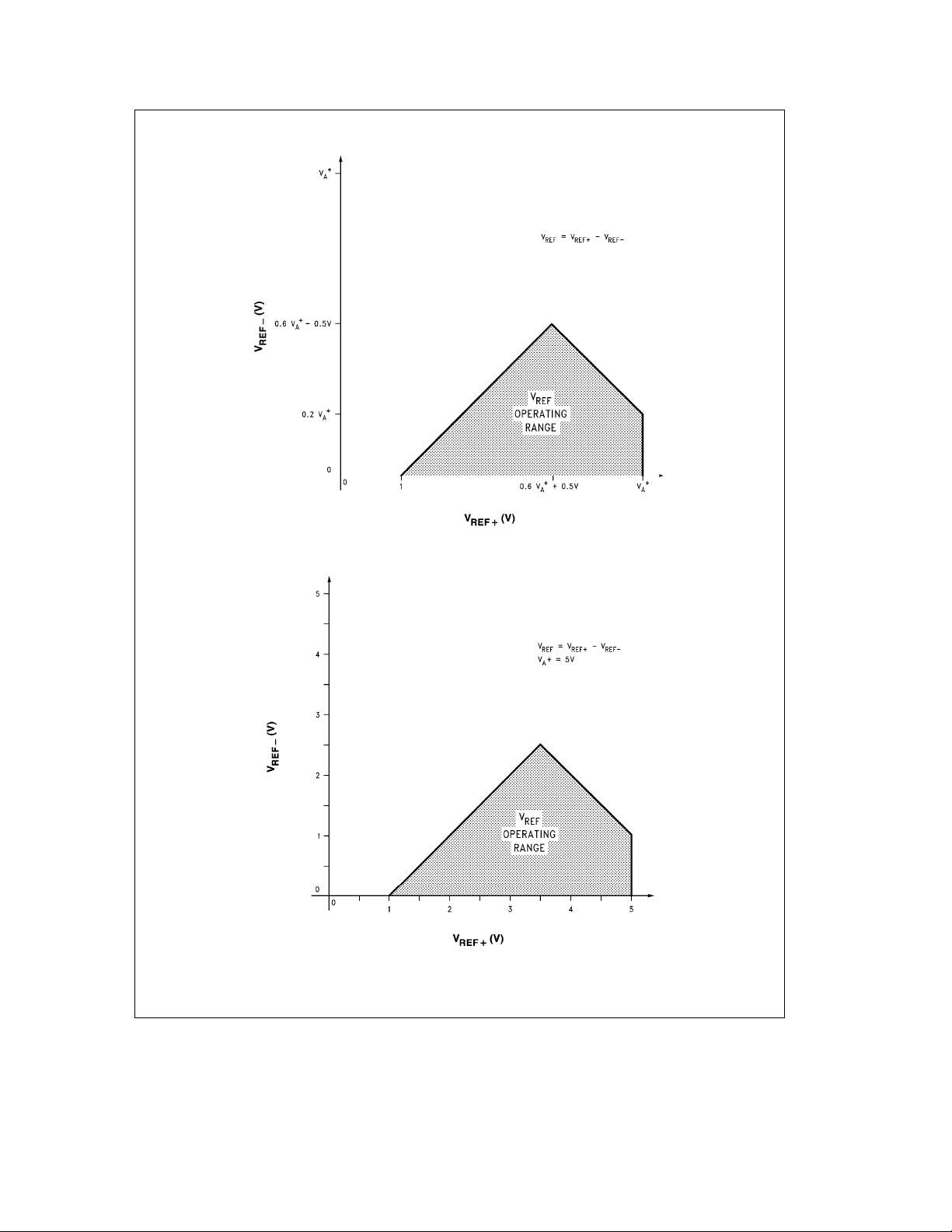
The reference voltage inputs are not fully differential. The
ADC12041 will not generate correct conversions if V
b
V
is below 1V.
REF
ship between V
REF
Figure 9
a
and V
shows the allowable relation-
b
.
REF
REF
b
e
a
and V
is an exam-
a
and
AGND,
REF
a
REF
b
FIGURE 9. V
Operating Range
REF
TL/H/12441– 43
OUTPUT DIGITAL CODE VERSUS ANALOG INPUT
VOLTAGE
The ADC12041’s fully differential 12-bit
a
sign ADC generates a two’s complement output that is found by using the
equation shown below:
a
b
b
(V
V
Output code
IN
e
(V
REF
) (4096)
IN
a
b
b
V
)
REF
Round off the result to the nearest integer value between -
–
*Tantalum
**Ceramic
FIGURE 8. Low Drift Extremely Stable Reference Circuit
Part Number
LM4041CI-Adj
LM4040AI-4.1
LM9140BYZ-4.1
LM368Y-5.0
Circuit of
Figure 8
Output Voltage Temperature
Tolerance Coefficient
g
0.5%
g
0.1%
g
0.5%
g
0.1%
Adjustable
g
100ppm/§C
g
100ppm/§C
g
25ppm/§C
g
20ppm/§C
g
2ppm/§C
25
TL/H/12441– 44
Page 26

Analog Application Information (Continued)
INPUT CURRENT
At the start of the acquisition window (t
ing current (due to capacitive switching) flows through the
analog input pins (ADCIN
a
and ADCINb). The peak value
AcqSYNOUT
of this input current will depend on the amplitude and frequency of the input voltage applied, the source impedance
and the ADCIN
a
and ADCINbinput switch ON resistance
of 2500X.
For low impedance voltage sources (1000
operation), the input charging current will decay to a value
that will not introduce any conversion errors before the end
of the default sample-and-hold (S/H) acquisition time
(9 clock cycles). For higher source impedances (1000
for 12 MHz operation), the S/H acquisition time should be
increased to allow the charging current to settle within specified limits. In asynchronous mode, the acquisition time may
be increased to 15, 47 or 79 clock cycles. If different acquisition times are needed, the synchronous mode can be
used to fully control the acquisition time.
INPUT BYPASS CAPACITANCE
External capacitors (0.01 mF – 0.1 mF) can be connected between the ADCIN
a
and ADCINbanalog input pins and the
analog ground to filter any noise caused by inductive pickup
associated with long leads.
POWER SUPPLY CONSIDERATIONS
Decoupling and bypassing the power supply on a high resolution ADC is an important design task. Noise spikes on the
a
V
(analog supply) or V
A
version errors. The analog comparator used in the ADC will
a
(digital supply) can cause con-
D
respond to power supply noise and will make erroneous
conversion decisions. The ADC is especially sensitive to
power supply spikes that occur during the auto-zero or linearity calibration cycles.
The ADC12041 is designed to operate from a single
power supply. The separate supply and ground pins for the
analog and digital portions of the circuit allow separate external bypassing. To minimize power supply noise and ripple, adequate bypass capacitors should be placed directly
between power supply pins and their associated grounds.
Both supply pins should be connected to the same supply
source. In systems with separate analog and digital supplies, the ADC should be powered from the analog supply.
At least a 10 mF tantalum electrolytic capacitor in parallel
with a 0.1 mF monolithic ceramic capacitor is recommended
for bypassing each power supply. The key consideration for
these capacitors is to have low series resistance and inductance. The capacitors should be placed as close as physically possible to the supply and ground pins with the smaller
capacitor closer to the device. The capacitors also should
have the shortest possible leads in order to minimize series
lead inductance. Surface mount chip capacitors are optimal
in this respect and should be used when possible.
When the power supply regulator is not local on the board,
adequate bypassing (a high value electrolytic capacitor)
should be placed at the power entry point. The value of the
capacitor depends on the total supply current of the circuits
) a charg-
k
X for 12 MHz
l
X
a
5V
on the PC board. All supply currents should be supplied by
the capacitor instead of being drawn from the external supply lines, while the external supply charges the capacitor at
a steady rate.
The ADC has two V
to use a 0.1 mFplusa10mF capacitor between pin
a
21(V
) and 22 (DGND) the SSOP and PLCC package.
D
The layout diagram in
a
and DGND pins. It is recommended
D
Figure 10
shows the recommended
placement for the supply bypass capacitors.
PC BOARD LAYOUT AND GROUNDING
CONSIDERATlONS
To get the best possible performance from the ADC12041,
the printed circuit boards should have separate analog and
digital ground planes. The reason for using two ground
planes is to prevent digital and analog ground currents from
sharing the same path until they reach a very low impedance power supply point. This will prevent noisy digital
switching currents from being injected into the analog
ground.
Figure 10
illustrates a favorable layout for ground planes,
power supply and reference input bypass capacitors. It
shows a layout using a 28-pin PLCC socket and throughhole assembly. A similar approach should be used for the
SSOP package.
The analog ground plane should encompass the area under
the analog pins and any other analog components such as
the reference circuit, input amplifiers, signal conditioning circuits, and analog signal traces.
The digital ground plane should encompass the area under
the digital circuits and the digital input/output pins of the
ADC12041. Having a continuous digital ground plane under
the data and clock traces is very important. This reduces
the overshoot/undershoot and high frequency ringing on
these lines that can be capacitively coupled to analog circuitry sections through stray capacitances.
The AGND and DGND in the ADC12041 are not internally
connected together. They should be connected together on
the PC board right at the chip. This will provide the shortest
return path for the signals being exchanged between the
internal analog and digital sections of the ADC.
It is also a good design practice to have power plane layers
in the PC board. This will improve the supply bypassing (an
effective distributed capacitance between power and
ground plane layers) and voltage drops on the supply lines.
However, power planes are not as essential as ground
planes are for satisfactory performance. If power planes are
used, they should be separated into two planes and the
area and connections should follow the same guidelines as
mentioned for the ground planes. Each power plane should
be laid out over its associated ground planes, avoiding any
overlap between power and ground planes of different
types. When the power planes are not used, it is recommended to use separate supply traces for the V
a
V
pins from a low impedance supply point (the regulator
D
output or the power entry point to the PC board). This will
a
and
A
help ensure that the noisy digital supply does not corrupt
the analog supply.
26
Page 27

Analog Application Information (Continued)
FIGURE 10. Top View of Printed Circuit Board for a 28-Pin PLCC ADC12041
When measuring AC input signals, any crosstalk between
analog input lines and the reference lines (ADCIN
g
V
) should be minimized. Crosstalk is minimized by re-
REF
ducing any stray capacitance between the lines. This can be
done by increasing the clearance between traces, keeping
the traces as short as possible, shielding traces from each
other by placing them on different sides of the AGND plane,
or running AGND traces between them.
Figure 10
also shows the reference input bypass capacitors.
Here the reference inputs are considered to be differential.
The performance improves by having a 0.1 mF capacitor
TL/H/12441– 45
g
manner similar to that described for the supply pins. When a
,
between the V
REF
a
and V
single ended reference is used, V
AGND and only two capacitors are used between V
b
and V
connect the AGND side of these capacitors to the V
(0.1 mFa10 mF). It is recommended to directly
REF
instead of connecting V
capacitors separately to the ground planes. This provides a
b
, and by bypassing in a
REF
b
is connected to
REF
b
and the ground sides of the
REF
REF
REF
a
b
significantly lower-impedance connection when using surface mount technology.
27
Page 28

28
Page 29

Physical Dimensions inches (millimeters)
28-Lead Molded Plastic Leaded Chip Carrier
Order Number ADC12041CIV
NS Package Number V28A
29
Page 30

Physical Dimensions inches (millimeters) (Continued)
28-Lead SSOP
Order Number ADC12041CIMSA
NS Package Number MSA28
LIFE SUPPORT POLICY
NATIONAL’S PRODUCTS ARE NOT AUTHORIZED FOR USE AS CRITICAL COMPONENTS IN LIFE SUPPORT
DEVICES OR SYSTEMS WITHOUT THE EXPRESS WRITTEN APPROVAL OF THE PRESIDENT OF NATIONAL
ADC12041 12-Bit Plus Sign 216 kHz Sampling Analog-to-Digital Converter
SEMICONDUCTOR CORPORATION. As used herein:
1. Life support devices or systems are devices or 2. A critical component is any component of a life
systems which, (a) are intended for surgical implant support device or system whose failure to perform can
into the body, or (b) support or sustain life, and whose be reasonably expected to cause the failure of the life
failure to perform, when properly used in accordance support device or system, or to affect its safety or
with instructions for use provided in the labeling, can effectiveness.
be reasonably expected to result in a significant injury
to the user.
National Semiconductor National Semiconductor National Semiconductor National Semiconductor
Corporation Europe Hong Kong Ltd. Japan Ltd.
1111 West Bardin Road Fax:
Arlington, TX 76017 Email: europe.support@nsc.com Ocean Centre, 5 Canton Rd. Fax: 81-043-299-2408
Tel: 1(800) 272-9959 Deutsch Tel:
Fax: 1(800) 737-7018 English Tel:
National does not assume any responsibility for use of any circuitry described, no circuit patent licenses are implied and National reserves the right at any time without notice to change said circuitry and specifications.
Fran3ais Tel:
Italiano Tel:
a
49 (0) 180-530 85 86 13th Floor, Straight Block, Tel: 81-043-299-2308
a
49 (0) 180-530 85 85 Tsimshatsui, Kowloon
a
49 (0) 180-532 78 32 Hong Kong
a
49 (0) 180-532 93 58 Tel: (852) 2737-1600
a
49 (0) 180-534 16 80 Fax: (852) 2736-9960
 Loading...