

Page 1
ADC12H030/ADC12H032/ADC12H034/ADC12H038,
ADC12030/ADC12032/ADC12034/ADC12038
Self-Calibrating 12-Bit Plus Sign Serial I/O
A/D Converters with MUX and Sample/Hold
January 1995
ADC12H030/ADC12H032/ADC12H034/ADC12H038,
ADC12030/ADC12032/ADC12034/ADC12038
Self-Calibrating 12-Bit Plus Sign Serial I/O A/D Converters with MUX and Sample/Hold
General Description
The ADC12030, and ADC12H030 families are 12-bit plus
sign successive approximation A/D converters with serial
I/O and configurable input multiplexers. The ADC12032/
ADC12H032, ADC12034/ADC12H034 and ADC12038/
ADC12H038 have 2, 4 and 8 channel multiplexers, respectively. The differential multiplexer outputs and A/D inputs
are available on the MUXOUT1, MUXOUT2, A/DIN1 and
A/DIN2 pins. The ADC12030/ADC12H030 has a two channel multiplexer with the multiplexer outputs and A/D inputs
internally connected. The ADC12030 family is tested with a
5 MHz clock, while the ADC12H030 family is tested with an
8 MHz clock. On request, these A/Ds go through a self
calibration process that adjusts linearity, zero and full-scale
errors to less than
g
1 LSB each.
The analog inputs can be configured to operate in various
combinations of single-ended, differential, or pseudo-differential modes. A fully differential unipolar analog input range
a
(0V to
5V) can be accommodated with a singlea5V supply. In the differential modes, valid outputs are obtained
even when the negative inputs are greater than the positive
because of the 12-bit plus sign output data format.
The serial I/O is configured to comply with the NSC
MICROWIRE
TM
. For complementary voltage references see
the LM4040, LM4041 or LM9140.
Applications
Y
Medical instruments
Y
Process control systems
Y
Test equipment
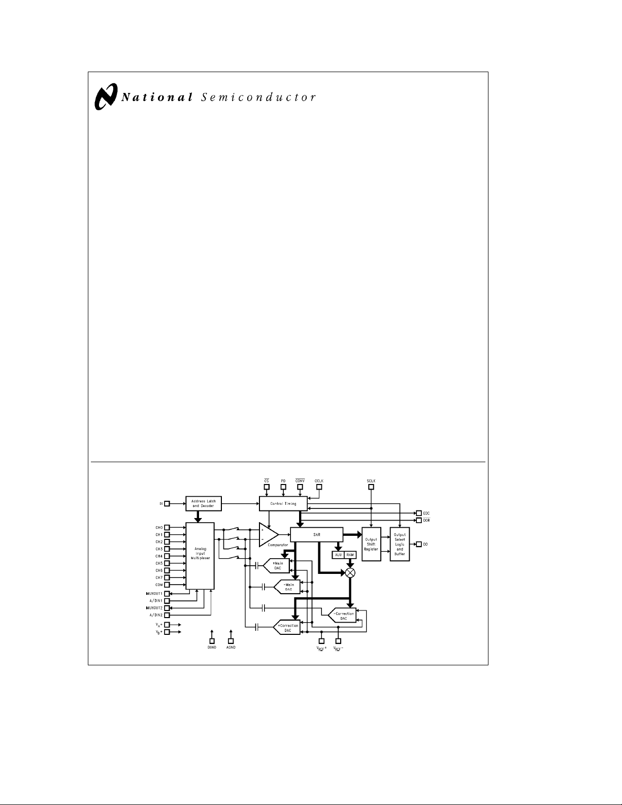
ADC12038 Simplified Block Diagram
Features
Y
Serial I/O (MICROWIRE Compatible)
Y
2, 4, or 8 channel differential or single-ended
multiplexer
Y
Analog input sample/hold function
Y
Power down mode
Y
Variable resolution and conversion rate
Y
Programmable acquisition time
Y
Variable digital output word length and format
Y
No zero or full scale adjustment required
Y
Fully tested and guaranteed with a 4.096V reference
Y
0V to 5V analog input range with single 5V power
supply
Y
No Missing Codes over temperature
Key Specifications
Y
Resolution 12-bit plus sign
Y
12-bit plus sign conversion time
Ð ADC12H030 family 5.5 ms (max)
Ð ADC12030 family 8.8 ms (max)
Y
12-bit plus sign throughput time
Ð ADC12H030 family 8.6 ms (max)
Ð ADC12030 family 14 ms (max)
Y
Integral linearity error
Y
Single supply 5Vg10%
Y
Power dissipation 33 mW (max)
Ð Power down 100 mW (typ)
g
1 LSB (max)
TRI-STATEÉis a registered trademark of National Semiconductor Corporation.
TM
COPS
microcontrollers, HPCTMand MICROWIRETMare trademarks of National Semiconductor Corporation.
C
1995 National Semiconductor Corporation RRD-B30M75/Printed in U. S. A.
TL/H/11354
TL/H/11354– 1
Page 2
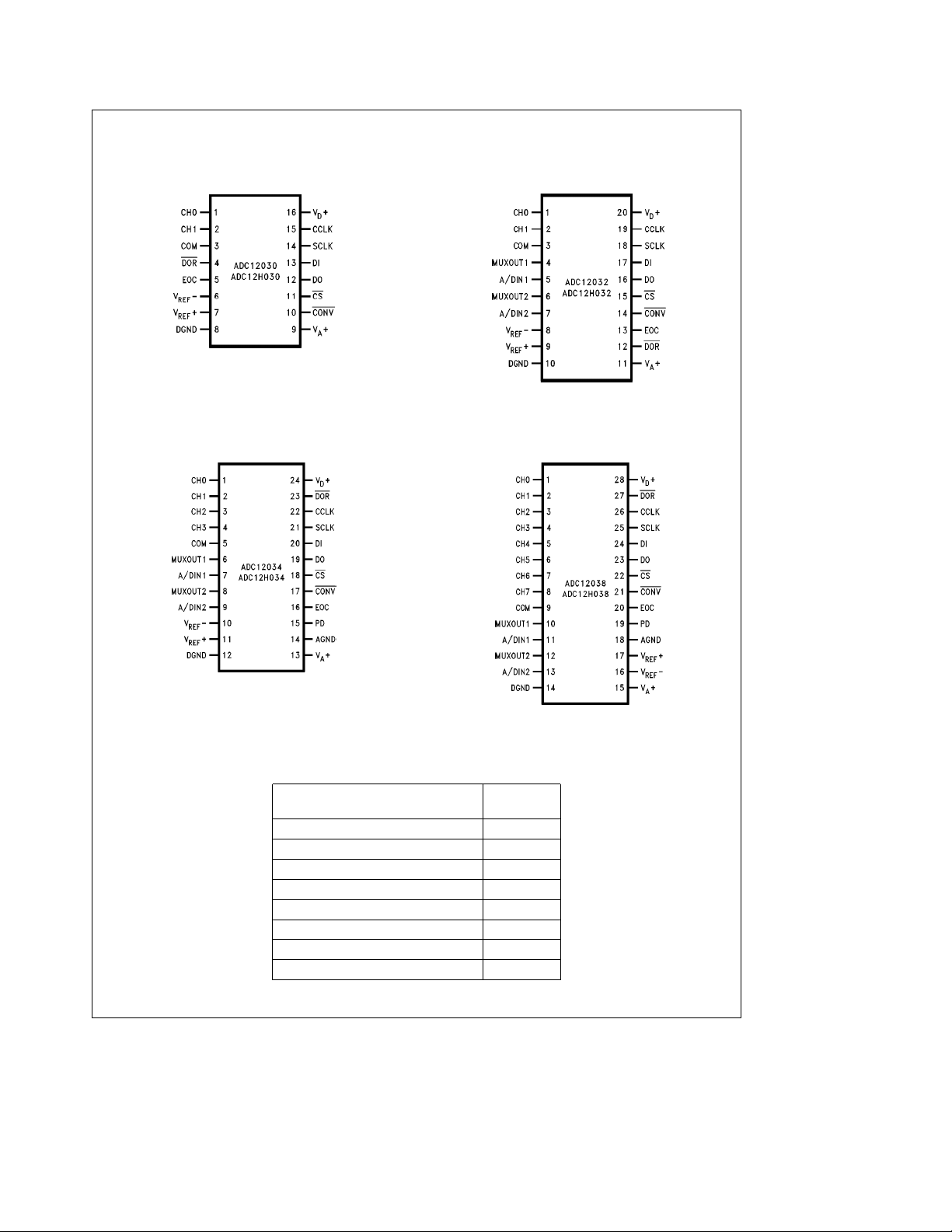
Connection Diagrams
16-Pin Dual-In-Line and
Wide Body SO Packages
Top View
24-Pin Dual-In-Line and
Wide Body SO Packages
TL/H/11354– 6
20-Pin Dual-In-Line and
Wide Body SO Packages
Top View
28-Pin Dual-In-Line and
Wide Body SO Packages
TL/H/11354– 7
Top View
Ordering Information
TL/H/11354– 8
Industrial Temperature Range
b
40§CsT
s
a
85§C
A
Package
ADC12H030CIN, ADC12030CIN N16E
ADC12H030CIWM, ADC12030CIWM M16B
ADC12H032CIN, ADC12032CIN N20A
ADC12H032CIWM, ADC12032CIWM M20B
ADC12H034CIN, ADC12034CIN N24C
ADC12H034CIWM, ADC12034CIWM M24B
ADC12H038CIN, ADC12038CIN N28B
ADC12H038CIWM, ADC12038CIWM M28B
2
Top View
TL/H/11354– 9
Page 3
Absolute Maximum Ratings (Notes1&2)
If Military/Aerospace specified devices are required,
please contact the National Semiconductor Sales
Office/Distributors for availability and specifications.
Positive Supply Voltage
a
a
e
(V
V
A
Voltage at Inputs and Outputs
except CH0–CH7 and COM
Voltage at Analog Inputs
CH0–CH7 and COM GND
a
b
V
V
l
A
D
Input Current at Any Pin (Note 3)
Package Input Current (Note 3)
Package Dissipation at
e
T
25§C (Note 4) 500 mW
A
ESD Susceptability (Note 5)
Human Body Model 1500V
Soldering Information
N Packages (10 seconds) 260
SO Package (Note 6):
Vapor Phase (60 seconds) 215
Infrared (15 seconds) 220
Storage Temperature
a
e
V
) 6.5V
D
0.3V to V
b
5V to V
a
a
a
300 mV
g
g
120 mA
0.3V
a
5V
30 mA
b
a
l
§
§
§
b
65§Ctoa150§C
Operating Ratings (Notes1&2)
Operating Temperature Range T
ADC12030CIN, ADC12030CIWM,
ADC12H030CIN, ADC12H030CIWM,
ADC12032CIN, ADC12032CIWM,
ADC12H032CIN, ADC12H032CIWM,
ADC12034CIN, ADC12034CIWM,
ADC12H034CIN, ADC12H034CIWM,
ADC12038CIN, ADC12038CIWM,
ADC12H038CIN,
ADC12H038CIWM
Supply Voltage (V
a
b
V
l
A
a
V
REF
b
V
REF
V
REF(VREF
V
Common Mode Voltage Range
REF
(V
REF
C
A/DIN1, A/DIN2, MUXOUT1
C
C
and MUXOUT2 Voltage Range 0V to V
A/D IN Common Mode Voltage Range
a
(V
IN
a
e
a
V
D
a
a
a
V
l
b
b
V
REF
b
V
)
REF
2
b
a
V
)
IN
2
s
s
T
MIN
b
a
e
A
40§CsT
a
V
D
a
)
T
A
s
a
A
4.5V toa5.5V
s
100 mV
0V to V
0V to V
REF
) 1VtoV
a
0.1 V
to 0.6 V
A
0V to V
MAX
85§C
A
A
A
A
A
a
a
a
a
a
a
Converter Electrical Characteristics
a
a
The following specifications apply for V
sign conversion mode, f
5 MHz for the ADC12030, ADC12032, ADC12034 and ADC12038, R
25X, fully-differential input with fixed 2.048V common-mode voltage, and 10(tCK) acquisition time unless otherwise specified.
Boldface limits apply for T
CK
e
f
SK
e
A
e
V
e
T
J
A
8 MHz for the ADC12H030, ADC12H032, ADC12H034 and ADC12H038, f
e
T
to T
MIN
a
e
ea
V
D
; all other limits T
MAX
5.0 VDC,V
S
Symbol Parameter Conditions
STATIC CONVERTER CHARACTERISTICS
Resolution with No Missing Codes 12asign Bits (min)
a
ILE Positive Integral Linearity Error After Auto-Cal (Notes 12, 18)
b
ILE Negative Integral Linearity Error After Auto-Cal (Notes 12, 18)
DNL Differential Non-Linearity After Auto-Cal
Positive Full-Scale Error After Auto-Cal (Notes 12, 18)
Negative Full-Scale Error After Auto-Cal (Notes 12, 18)
Offset Error After Auto-Cal (Notes 5, 18)
(a)eVIN(b)e2.048V
V
IN
DC Common Mode Error After Auto-Cal (Note 15)
TUE Total Unadjusted Error After Auto-Cal
(Notes 12, 13 and 14)
Resolution with No Missing Codes 8-bitasign mode 8asign Bits (min)
a
INL Positive Integral Linearity Error 8-bitasign mode (Note 12)
b
INL Negative Integral Linearity Error 8-bitasign mode (Note 12)
DNL Differential Non-Linearity 8-bitasign mode
Positive Full-Scale Error 8-bitasign mode (Note 12)
a
ea
REF
e
25X, source impedance for V
e
T
A
4.096 VDC,V
e
25§C. (Notes 7, 8 and 9)
J
Typical
(Note 10)
g
1/2
g
1/2
g
1/2
g
1/2
g
1/2
g
2
g
1 LSB
b
e
0VDC, 12-bit
REF
REF
a
CK
and V
e
Limits
(Note 11)
g
1 LSB (max)
g
1 LSB (max)
g
1 LSB (max)
g
3.0 LSB (max)
g
3.0 LSB (max)
g
2 LSB (max)
g
3.5 LSB (max)
g
1/2 LSB (max)
g
1/2 LSB (max)
g
3/4 LSB (max)
g
1/2 LSB (max)
REF
(Limits)
f
SK
b
Units
a
e
s
3
Page 4
Converter Electrical Characteristics (Continued)
a
a
e
The following specifications apply for V
sign conversion mode, f
5 MHz for the ADC12030, ADC12032, ADC12034 and ADC12038, R
25X, fully-differential input with fixed 2.048V common-mode voltage, and 10(tCK) acquisition time unless otherwise specified.
Boldface limits apply for T
CK
e
e
f
SK
e
T
A
J
V
A
8 MHz for the ADC12H030, ADC12H032, ADC12H034 and ADC12H038, f
e
T
to T
MIN
a
e
ea
V
D
; all other limits T
MAX
5.0 VDC,V
S
Symbol Parameter Conditions
STATIC CONVERTER CHARACTERISTICS (Continued)
Negative Full-Scale Error 8-bitasign mode (Note 12)
Offset Error 8-bitasign mode,
after Auto-Zero (Note 13)
V
(a)eVIN(b)
IN
ea
TUE Total Unadjusted Error 8-bitasign mode
after Auto-Zero
(Notes 12, 13 and 14)
Multiplexer Channel to Channel
Matching
a
Power Supply Sensitivity V
Offset Error
a
Full-Scale Error
b
Full-Scale Error
a
Integral Linearity Error
b
Integral Linearity Error
ea
5Vg10%
ea
V
REF
4.096V
Output Data from (Note 20)
‘‘12-Bit Conversion of Offset’’
(see Table V)
Output Data from (Note 20)
‘‘12-Bit Conversion of Full-Scale’’
(see Table V)
UNIPOLAR DYNAMIC CONVERTER CHARACTERISTICS
S/(NaD) Signal-to-Noise Plus f
Distortion Ratio f
b
3 dB Full Power Bandwidth V
e
1 kHz, V
IN
e
20 kHz, V
IN
e
f
40 kHz, V
IN
e
5VPP, where S/(NaD) drops 3 dB 31 kHz
IN
IN
e
IN
IN
5VPP,V
e
5VPP,V
e
5VPP,V
DIFFERENTIAL DYNAMIC CONVERTER CHARACTERISTICS
S/(NaD) Signal-to-Noise Plus f
Distortion Ratio f
b
3 dB Full Power Bandwidth V
IN
IN
f
IN
e
e
e
IN
1 kHz, V
20 kHz, V
40 kHz, V
e
g
e
g
5V, V
IN
e
g
5V, V
IN
e
g
5V, V
IN
5V, where S/(NaD) drops 3 dB 40 kHz
a
ea
REF
e
25X, source impedance for V
e
T
A
4.096 VDC,V
e
25§C. (Notes 7, 8 and 9)
J
Typical
(Note 10)
2.048V
a
e
5.0V 69.4 dB
REF
a
e
5.0V 68.3 dB
REF
a
e
5.0V 65.7 dB
REF
a
e
5.0V 77.0 dB
REF
a
e
5.0V 73.9 dB
REF
a
e
5.0V 67.0 dB
REF
b
e
0VDC, 12-bit
REF
REF
a
CK
and V
e
REF
Limits
(Note 11)
g
1/2 LSB (max)
g
1/2 LSB (max)
g
3/4 LSB (max)
g
0.05 LSB
g
0.5
g
0.5
g
0.5
g
0.5 LSB
g
0.5 LSB
g
1 LSB (max)
g
1.5 LSB (max)
g
1.5 LSB (max)
a
10 LSB (max)
b
10 LSB (min)
4095 LSB (max)
4093 LSB (min)
a
e
f
SK
b
Units
(Limits)
s
4
Page 5
Electrical Characteristics
a
a
The following specifications apply for V
sign conversion mode, f
5 MHz for the ADC12030, ADC12032, ADC12034 and ADC12038, R
25X, fully-differential input with fixed 2.048V common-mode voltage, and 10(tCK) acquisition time unless otherwise specified.
Boldface limits apply for T
CK
e
f
SK
e
A
e
V
e
T
J
A
8 MHz for the ADC12H030, ADC12H032, ADC12H034 and ADC12H038, f
e
T
to T
MIN
a
e
ea
V
D
; all other limits T
MAX
5.0 VDC,V
Symbol Parameter Conditions
REFERENCE INPUT, ANALOG INPUTS AND MULTIPLEXER CHARACTERISTICS
C
REF
C
A/D
Reference Input Capacitance 85 pF
A/DIN1 and A/DIN2 Analog Input
Capacitance
A/DIN1 and A/DIN2 Analog Input V
Leakage Current V
IN
IN
ea
e
0V
5.0V or
CH0–CH7 and COM Input Voltage GNDb0.05 V (min)
C
CH
C
MUXOUT
CH0–CH7 and COM Input Capacitance 10 pF
MUX Output Capacitance 20 pF
Off Channel Leakage (Note 16) On Channele5V and
CH0–CH7 and COM Pins Off Channel
e
On Channele0V and
Off Channele5V
On Channel Leakage (Note 16) On Channele5V and
CH0–CH7 and COM Pins Off Channel
e
On Channele0V and
e
2.5V and
e
2.5V and
e
5V
e
e
5.0V or
e
0V
e
2.4V
e
2.4V
PP,fIN
Off Channel
MUXOUT1 and MUXOUT2 V
Leakage Current V
R
ON
MUX On Resistance V
RONMatching Channel to Channel V
Channel to Channel Crosstalk V
MUXOUT
MUXOUT
IN
V
MUXOUT
IN
V
MUXOUT
IN
MUX Bandwidth 90 kHz
a
ea
REF
e
25X, source impedance for V
S
e
T
A
4.096 VDC,V
e
25§C. (Notes 7, 8 and 9)
J
Typical Limits Units
(Note 10) (Note 11) (Limits)
75 pF
g
0.1
b
0V
0.01
0.01 0.3 mA (max)
0V
5V
0.01 0.3 mA (max)
b
0.01
0.01 0.3 mA (max)
850 1150 X (max)
5%
e
40 kHz
b
72 dB
b
e
0VDC, 12-bit
REF
a
and V
REF
g
1.0 mA (max)
a
a
V
0.05 V (max)
A
b
0.3 mA (min)
b
0.3 mA (min)
CK
e
REF
a
e
f
SK
b
s
5
Page 6
DC and Logic Electrical Characteristics
a
a
The following specifications apply for V
sign conversion mode, f
5 MHz for the ADC12030, ADC12032, ADC12034 and ADC12038, R
25X, fully-differential input with fixed 2.048V common-mode voltage, and 10(tCK) acquisition time unless otherwise specified.
Boldface limits apply for T
CK
e
f
SK
e
A
e
V
e
T
J
A
8 MHz for the ADC12H030, ADC12H032, ADC12H034 and ADC12H038, f
e
T
to T
MIN
a
e
ea
V
D
; all other limits T
MAX
5.0 VDC,V
S
Symbol Parameter Conditions
CCLK, CS, CONV, DI, PD AND SCLK INPUT CHARACTERISTICS
a
V
V
I
IN(1)
I
IN(0)
Logical ‘‘1’’ Input Voltage V
IN(1)
Logical ‘‘0’’ Input Voltage V
IN(0)
Logical ‘‘1’’ Input Current V
Logical ‘‘0’’ Input Current V
e
5.5V 2.0 V (min)
a
e
4.5V 0.8 V (max)
e
5.0V 0.005 1.0 mA (max)
IN
e
0V
IN
DO, EOC AND DOR DIGITAL OUTPUT CHARACTERISTICS
V
OUT(1)
V
OUT(0)
I
OUT
a
b
Logical ‘‘1’’ Output Voltage V
Logical ‘‘0’’ Output Voltage V
TRI-STATE Output Current V
I
Output Short Circuit Source Current V
SC
I
Output Short Circuit Sink Current V
SC
V
V
a
a
OUT
OUT
OUT
OUT
e
e
e
4.5V, I
4.5V, I
4.5V, I
e
e
e
e
eb
OUT
eb
OUT
e
OUT
0V
5V 0.1 3.0 mA (max)
0V 14 6.5 mA (min)
a
V
D
a
POWER SUPPLY CHARACTERISTICS
a
I
D
Digital Supply Current Awake 1.6 2.5 mA (max)
ADC12030, ADC12032, ADC12034 CS
and ADC12038 CS
e
HIGH, Powered Down, CCLK on 600 mA
e
HIGH, Powered Down, CCLK off 20 mA
Digital Supply Current Awake 2.3 3.2 mA
e
HIGH, Powered Down, CCLK on 0.9 mA
e
HIGH, Powered Down, CCLK off 20 mA
e
CS
HIGH, Powered Down, CCLK on 10 mA
e
CS
HIGH, Powered Down, CCLK off 0.1 mA
e
CS
HIGH, Powered Down 0.1 mA
I
I
A
REF
ADC12H030, ADC12H032, ADC12H034 CS
and ADC12H038 CS
a
Positive Analog Supply Current Awake 2.7 4.0 mA (max)
Reference Input Current Awake 70 mA
a
ea
REF
e
25X, source impedance for V
e
T
A
4.096 VDC,V
e
25§C. (Notes 7, 8 and 9)
J
REF
b
REF
e
a
0VDC, 12-bit
e
CK
and V
REF
Typical Limits Units
(Note 10) (Note 11) (Limits)
b
0.005
b
1.0 mA (min)
360 mA 2.4 V (min)
10 mA 4.25 V (min)
1.6 mA 0.4 V (max)
b
0.1
b
3.0 mA (max)
16 8.0 mA (min)
a
e
f
SK
b
s
6
Page 7
AC Electrical Characteristics
a
a
e
The following specifications apply for V
sign conversion mode, t
e
f
CK
V
specified. Boldface limits apply for T
e
f
5 MHz for the ADC12030, ADC12032, ADC12034 and ADC12038, R
SK
b
s
25X, fully-differential input with fixed 2.048V common-mode voltage, and 10(tCK) acquisition time unless otherwise
REF
e
e
t
3 ns, f
r
f
CK
e
A
Symbol Parameter Conditions
f
f
Conversion Clock 10 85MHz (max)
CK
(CCLK) Frequency 1 MHz (min)
Serial Data Clock 10 85MHz (max)
SK
SCLK Frequency 0 Hz (min)
Conversion Clock 40 40 % (min)
Duty Cycle 60 60 % (max)
Serial Data Clock 40 40 % (min)
Duty Cycle 60 60 % (max)
t
Conversion Time 12-BitaSign or 12-Bit 44(tCK) 44(tCK) 44(tCK) (max)
C
8-BitaSign or 8-Bit 21(tCK) 21(tCK) 21(tCK) (max)
t
Acquisition Time 6 Cycles Programmed 6(tCK) 6(tCK) 6(tCK) (min)
A
(Note 19) 7(t
10 Cycles Programmed 10(tCK) 10(tCK) 10(tCK) (min)
18 Cycles Programmed 18(tCK) 18(tCK) 18(tCK) (min)
34 Cycles Programmed 34(tCK) 34(tCK) 34(tCK) (min)
t
t
t
Self-Calibration Time 4944(tCK) 4944(tCK) 4944(tCK) (max)
CKAL
Auto-Zero Time 76(tCK) 76(tCK) 76(tCK) (max)
AZ
Self-Calibration or 2(tCK) 2(tCK) 2(tCK) (min)
SYNC
Auto-Zero Synchronization 3(t
Time from DOR
t
DOR High Time 9(tSK) 9(tSK) 9(tSK) (max)
DOR
when CS is Low
Continuously for Read
Data and Software
Power Up/Down
t
CONV Valid Data Time 8(tSK) 8(tSK) 8(tSK) (max)
CONV
e
V
A
e
e
f
SK
e
T
T
J
MIN
a
ea
V
8 MHz for the ADC12H030, ADC12H032, ADC12H034 and ADC12H038,
D
to T
MAX
5.0 VDC,V
; all other limits T
Typical
(Note 10)
REF
a
ea
4.096 VDC,V
e
25X, source impedance for V
S
e
e
T
A
25§C. (Note 17)
J
REF
b
e
0VDC, 12-bit
ADC12H030/2/4/8 ADC12030/2/4/8
Limits Limits
(Note 11) (Note 11)
REF
(Limits)
a
and
Units
5.5 8.8 ms (max)
2.625 4.2 ms (max)
) 7(tCK) (max)
CK
0.75 1.2 ms (min)
0.875 1.4 ms (max)
) 11(tCK) (max)
11(t
CK
1.25 2.0 ms (min)
1.375 2.2 ms (max)
) 19(tCK) (max)
19(t
CK
2.25 3.6 ms (min)
2.375 3.8 ms (max)
) 35(tCK) (max)
35(t
CK
4.25 6.8 ms (min)
4.375 7.0 ms (max)
618.0 988.8 ms (max)
9.5 15.2 ms (max)
) 3(tCK) (max)
CK
0.250 0.40 ms (min)
0.375 0.60 m s (max)
1.125 1.8 ms (max)
1.0 1.6 ms (max)
a
7
Page 8
AC Electrical Characteristics (Continued)
a
a
e
The following specifications apply for V
sign conversion mode, t
e
f
CK
V
specified. Boldface limits apply for T
e
f
5 MHz for the ADC12030, ADC12032, ADC12034 and ADC12038, R
SK
b
s
25X, fully-differential input with fixed 2.048V common-mode voltage, and 10(tCK) acquisition time unless otherwise
REF
e
e
t
3 ns, f
r
f
V
A
e
f
CK
e
T
A
J
Symbol Parameter Conditions
t
HPU
t
SPU
Hardware Power-Up Time, Time from
PD Falling Edge to EOC Rising Edge
Software Power-Up Time, Time from
Serial Data Clock Falling Edge to 140 250 ms (max)
EOC Rising Edge
t
ACC
t
SET-UP
t
DELAY
t1H,t
t
HDI
t
SDI
t
HDO
t
DDO
t
RDO
t
FDO
t
CD
t
SD
C
IN
C
OUT
Access Time Delay from
CS
Falling Edge to DO Data Valid
Set-Up Time of CS Falling Edge to
Serial Data Clock Rising Edge
Delay from SCLK Falling
Edge to CS
Delay from CS Rising Edge to R
0H
DO TRI-STATE
Falling Edge
É
DI Hold Time from Serial Data
Clock Rising Edge
DI Set-Up Time from Serial Data
Clock Rising Edge
DO Hold Time from Serial Data R
Clock Falling Edge 5 ns (min)
Delay from Serial Data Clock
Falling Edge to DO Data Valid
DO Rise Time, TRI-STATE to High R
DO Rise Time, Low to High 10 30 ns (max)
DO Fall Time, TRI-STATE to Low R
DO Fall Time, High to Low 12 30 ns (max)
Delay from CS Falling Edge
to DOR
Falling Edge
Delay from Serial Data Clock Falling
Edge to DOR
Rising Edge
Capacitance of Logic Inputs 10 pF
Capacitance of Logic Outputs 20 pF
a
e
ea
V
D
e
8 MHz for the ADC12H030, ADC12H032, ADC12H034 and ADC12H038,
SK
e
T
MIN
to T
L
L
L
L
MAX
e
e
e
e
5.0 VDC,V
; all other limits T
e
3k, C
L
e
3k, C
L
e
3k, C
L
e
3k, C
L
REF
a
ea
4.096 VDC,V
e
25X, source impedance for V
S
e
e
T
A
25§C. (Note 17)
J
REF
b
e
0VDC, 12-bit
a
REF
and
Typical Limits Units
(Note 10) (Note 11) (Limits)
140 250 ms (max)
20 50 ns (max)
30 ns (min)
0 5 ns (min)
100 pF
40 100 ns (max)
5 15 ns (min)
5 10 ns (min)
100 pF
25
50 ns (max)
35 50 ns (max)
100 pF 10 30 ns (max)
100 pF 12 30 ns (max)
25 45 ns (max)
25 45 ns (max)
a
8
Page 9
Electrical Characteristics (Continued)
Note 1: Absolute Maximum Ratings indicate limits beyond which damage to the device may occur. Operating Ratings indicate conditions for which the device is
functional, but do not guarantee specific performance limits. For guaranteed specifications and test conditions, see the Electrical Characteristics. The guaranteed
specifications apply only for the test conditions listed. Some performance characteristics may degrade when the device is not operated under the listed test
conditions.
Note 2: All voltages are measured with respect to GND, unless otherwise specified.
Note 3: When the input voltage (V
The 120 mA maximum package input current rating limits the number of pins that can safely exceed the power supplies with an input current of 30 mA to four.
Note 4: The maximum power dissipation must be derated at elevated temperatures and is dictated by T
allowable power dissipation at any temperature is P
maxe150§C. The typical thermal resistance (HJA) of these parts when board mounted follow:
device, T
J
) at any pin exceeds the power supplies (V
IN
e
(TJmaxbTA)/iJAor the number given in the Absolute Maximum Ratings, whichever is lower. For this
D
IN
k
GND or V
Part Number Resistance
ADC12H030CIN, ADC12030CIN 53§C/W
ADC12H030CIWM, ADC12030CIWM 70§C/W
ADC12H032CIN, ADC12032CIN 46§C/W
ADC12H032CIWM, ADC12032CIWM 64§C/W
ADC12H034CIN, ADC12034CIN 42§C/W
ADC12H034CIWM, ADC12034CIWM 57§C/W
ADC12H038CIN, ADC12038CIN 40§C/W
ADC12H038CIWM, ADC12038CIWM 50§C/W
Note 5: The human body model is a 100 pF capacitor discharged through a 1.5 kX resistor into each pin.
Note 6: See AN450 ‘‘Surface Mounting Methods and Their Effect on Product Reliability’’ or the section titled ‘‘Surface Mount’’ found in any post 1986 National
Semiconductor Linear Data Book for other methods of soldering surface mount devices.
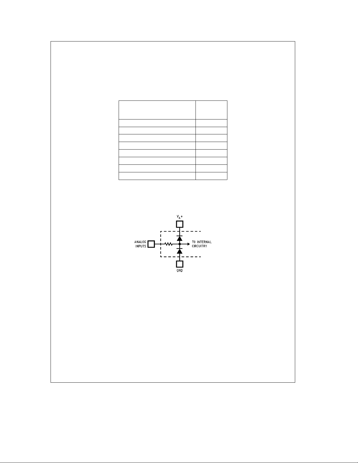
Note 7: Two on-chip diodes are tied to each analog input through a series resistor as shown below. Input voltage magnitude up to 5V above V
will not damage this device. However, errors in the A/D conversion can occur (if these diodes are forward biased by more than 50 mV) if the input voltage
magnitude of selected or unselected analog input go above V
s
4.55 VDCto ensure accurate conversions.
must be
a
or below GND by more than 50 mV. As an example, if V
A
a
l
IN
a
V
or V
), the current at that pin should be limited to 30 mA.
A
D
max, iJAand the ambient temperature, TA. The maximum
J
Thermal
i
JA
a
is 4.5 VDC, full-scale input voltage
A
a
or 5V below GND
A
a
Note 8: To guarantee accuracy, it is required that the V
pin.
Note 9: With the test condition for V
e
a
J
1 (see
T
A
e
Figure 2
Note 10: Typicals are at T
Note 11: Tested limits are guaranteed to National’s AOQL (Average Outgoing Quality Level).
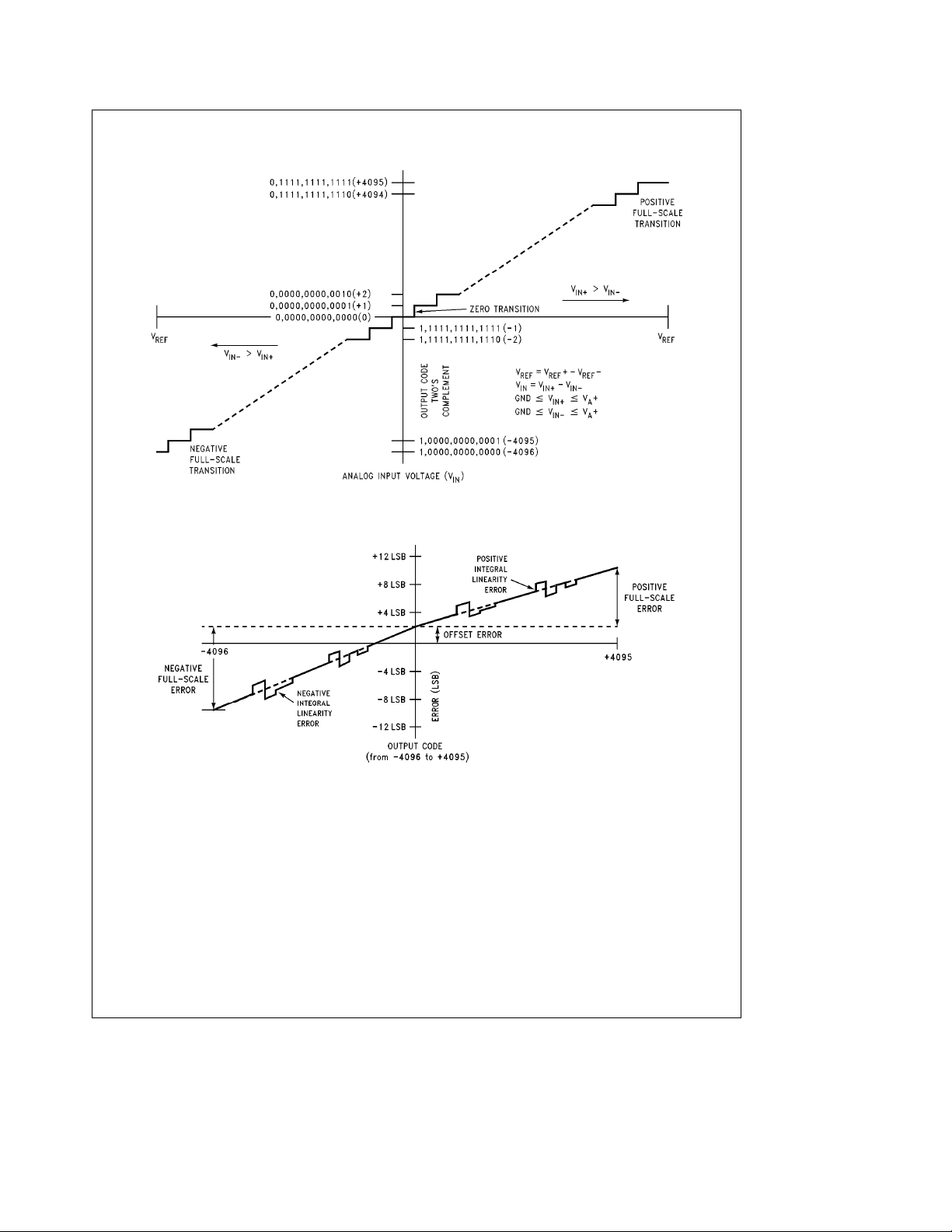
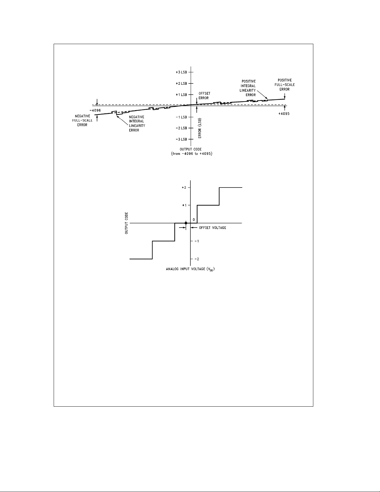
Note 12: Positive integral linearity error is defined as the deviation of the analog value, expressed in LSBs, from the straight line that passes through positive full-
scale and zero. For negative integral linearity error, the straight line passes through negative full-scale and zero (see
Note 13: Zero error is a measure of the deviation from the mid-scale voltage (a code of zero), expressed in LSB. It is the worst-case value of the code transitions
between 1 to 0 and 0 to
a
b
REF(VREF
25§C and represent most likely parametric norm.
V
).
a
and V
A
REF
be connected together to the same power supply with separate bypass capacitors at each V
D
b
) given asa4.096V, the 12-bit LSB is 1.0 mV and the 8-bit LSB is 16.0 mV.
TL/H/11354– 2
Figures 1b
and1c).
Note 14: Total unadjusted error includes offset, full-scale, linearity and multiplexer errors.
Note 15: The DC common-mode error is measured in the differential multiplexer mode with the assigned positive and negative input channels shorted together.
Note 16: Channel leakage current is measured after the channel selection.
Note 17: Timing specifications are tested at the TTL logic levels, V
to 1.4V.
Note 18: The ADC12030 family’s self-calibration technique ensures linearity and offset errors as specified, but noise inherent in the self-calibration process will
result in a maximum repeatability uncertainty of 0.2 LSB.
Note 19: If SCLK and CCLK are driven from the same clock source, then t
Note 20: The ‘‘12-Bit Conversion of Offset’’ and ‘‘12-Bit Conversion of Full-Scale’’ modes are intended to test the functionality of the device. Therefore, the output
data from these modes are not an indication of the accuracy of a conversion result.
e
0.4V for a falling edge and V
IL
is 6, 10, 18 or 34 clock periods minimum and maximum.
A
e
2.4V for a rising edge. TRI-STATE output voltage is forced
IH
9
a
Page 10
Electrical Characteristics (Continued)
FIGURE 1a. Transfer Characteristic
FIGURE 1b. Simplified Error Curve vs Output Code without Auto-Calibration or Auto-Zero Cycles
TL/H/11354– 10
TL/H/11354– 11
10
Page 11
Electrical Characteristics (Continued)
FIGURE 1c. Simplified Error Curve vs Output Code after Auto-Calibration Cycle
TL/H/11354– 13
FIGURE 2. Offset or Zero Error Voltage
TL/H/11354– 12
11
Page 12
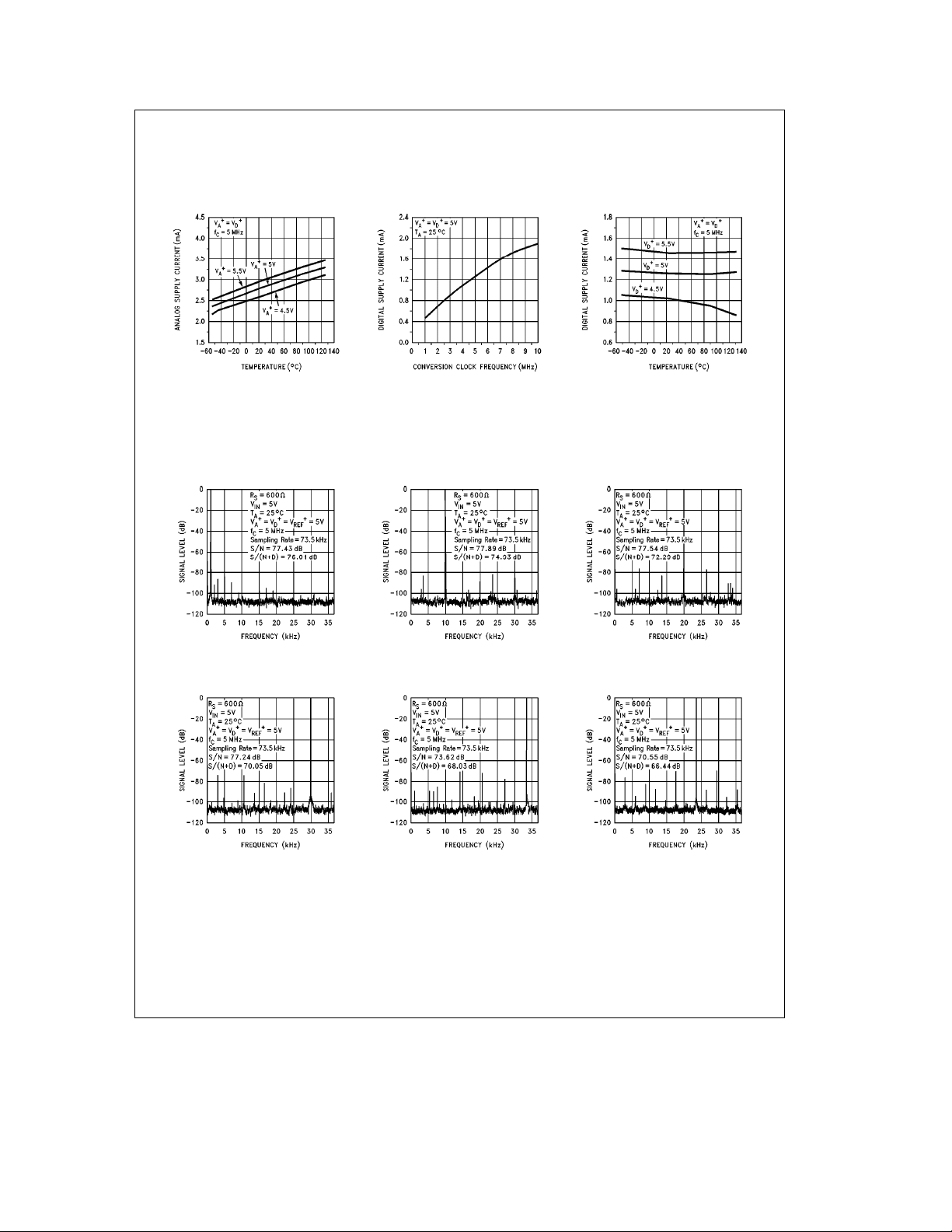
Typical Performance Characteristics
The following curves apply for 12-bitasign mode after auto-calibration unless otherwise specified. The performance for 8-bit
sign mode is equal to or better than shown. (Note 9)
a
Linearity Error Change
vs Clock Frequency
Linearity Error Change
vs Supply Voltage
Full-Scale Error Change
vs Reference Voltage
Linearity Error Change
vs Temperature
Full-Scale Error Change
vs Clock Frequency
Full-Scale Error Change
vs Supply Voltage
Linearity Error Change
vs Reference Voltage
Full-Scale Error Change
vs Temperature
Zero Error Change
vs Clock Frequency
Zero Error Change
vs Temperature
Zero Error Change
vs Reference Voltage
12
Zero Error Change
vs Supply Voltage
TL/H/11354– 14
Page 13
Typical Performance Characteristics (Continued)
The following curves apply for 12-bit
sign mode is equal to or better than shown.
a
sign mode after auto-calibration unless otherwise specified. The performance for 8-bit
a
Analog Supply Current
vs Temperature
Digital Supply Current
vs Clock Frequency
Digital Supply Current
vs Temperature
Typical Dynamic Performance Characteristics
The following curves apply for 12-bitasign mode after auto-calibration unless otherwise specified.
Bipolar Spectral Response
with 1 kHz Sine Wave Input
Bipolar Spectral Response
with 10 kHz Sine Wave Input
Bipolar Spectral Response
with 20 kHz Sine Wave Input
TL/H/11354– 15
Bipolar Spectral Response
with 30 kHz Sine Wave Input
Bipolar Spectral Response
with 40 kHz Sine Wave Input
13
Bipolar Spectral Response
with 50 kHz Sine Wave Input
TL/H/11354– 16
Page 14

Typical Dynamic Performance Characteristics (Continued)
The following curves apply for 12-bit
Bipolar Spurious Free
Dynamic Range
Unipolar Signal-to-Noise
a
Distortion Ratio
vs Input Signal Level
a
sign mode after auto-calibration unless otherwise specified.
Unipolar Signal-to-Noise Ratio
vs Input Frequency
Unipolar Spectral Response
with 1 kHz Sine Wave Input
Unipolar Signal-to-Noise
a
Distortion Ratio
vs Input Frequency
Unipolar Spectral Response
with 10 kHz Sine Wave Input
Unipolar Spectral Response
with 20 kHz Sine Wave Input
Unipolar Spectral Response
with 30 kHz Sine Wave Input
Unipolar Spectral Response
with 50 kHz Sine Wave Input
14
Unipolar Spectral Response
with 40 kHz Sine Wave Input
TL/H/11354– 17
Page 15

Test Circuits
DO ‘‘TRI-STATE’’ (t1H,t0H)
Timing Diagrams
DO Falling and Rising Edge
DO except ‘‘TRI-STATE’’
TL/H/11354– 3
TL/H/11354– 4
Leakage Current
TL/H/11354– 5
DO ‘‘TRI-STATE’’ Falling and Rising Edge
TL/H/11354– 18
DI Data Input Timing
TL/H/11354– 19
TL/H/11354– 20
15
Page 16

Timing Diagrams (Continued)
DO Data Output Timing with CS Continuously Low
DO Data Output Timing Using CS
TL/H/11354– 21
Note: DO output data is not valid during this cycle.
TL/H/11354– 22
ADC12038 Auto Cal or Auto Zero
TL/H/11354– 23
16
Page 17

Timing Diagrams (Continued)
ADC12038 Read Data without Starting a Conversion Using CS
ADC12038 Read Data without Starting a Conversion with CS Continuously Low
TL/H/11354– 24
TL/H/11354– 25
17
Page 18

Timing Diagrams (Continued)
ADC12038 Conversion Using CS
with 8-Bit Digital Output Format
ADC12038 Conversion Using CS with 16-Bit Digital Output Format
TL/H/11354– 26
TL/H/11354– 51
18
Page 19

Timing Diagrams (Continued)
ADC12038 Conversion with CS
Continuously Low and 8-Bit Digital Output Format
ADC12038 Conversion with CS Continuously Low and 16-Bit Digital Output Format
TL/H/11354– 28
TL/H/11354– 29
19
Page 20

Timing Diagrams (Continued)
ADC12038 Software Power Up/Down Using CS
with 16-Bit Digital Output Format
ADC12038 Software Power Up/Down with CS Continuously Low and 16-Bit Digital Output Format
TL/H/11354– 52
TL/H/11354– 31
20
Page 21

Timing Diagrams (Continued)
ADC12038 Hardware Power Up/Down
Note: Hardware power up/down may occur at any time. If PD is high while a conversion is in progress that conversion will be corrupted and erroneous data will be
stored in the output shift register.
TL/H/11354– 32
ADC12038 Configuration ModificationÐExample of a Status Read
Note: In order for all 9 bits of Status Information to be accessible, the last conversion programmed before Cycle N needs to have a resolution of 8 bits plus sign, 12
bits, 12 bits plus sign, or greater.
TL/H/11354– 33
21
Page 22

Pin Descriptions
CCLK The clock applied to this input controls the su-
SCLK This is the serial data clock input. The clock
DI This is the serial data input pin. The data ap-
DO The data output pin. This pin is an active push/
EOC This pin is an active push/pull output and indi-
CS
cessive approximation conversion time interval
and the acquisition time. The rise and fall times
of the clock edges should not exceed 1 ms.
applied to this input controls the rate at which
the serial data exchange occurs. The rising
edge loads the information on the DI pin into
the multiplexer address and mode select shift
register. This address controls which channel of
the analog input multiplexer (MUX) is selected
and the mode of operation for the A/D. With CS
low the falling edge of SCLK shifts the data resulting from the previous ADC conversion out
on DO, with the exception of the first bit of data.
When CS
is low continously, the first bit of the
data is clocked out on the rising edge of EOC
(end of conversion). When CS
falling edge of CS
of data. CS
always clocks out the first bit
should be brought low when SCLK
is toggled the
is low. The rise and fall times of the clock edges
should not exceed 1 ms.
plied to this pin is shifted by the rising edge of
SCLK into the multiplexer address and mode
select register. Tables II through V show the assignment of the multiplexer address and the
mode select data.
pull output when CS
is low. When CS is high,
this output is TRI-STATE. The A/D conversion
result (D0 –D12) and converter status data are
clocked out by the falling edge of SCLK on this
pin. The word length and format of this result
can vary (see Table I). The word length and format are controlled by the data shifted into the
multiplexer address and mode select register
(see Table V).
cates the status of the ADC12030/2/4/8.
When low, it signals that the A/D is busy with a
conversion, auto-calibration, auto-zero or power
down cycle. The rising edge of EOC signals the
end of one of these cycles.
This is the chip select pin. When a logic low is
applied to this pin, the rising edge of SCLK
shifts the data on DI into the address register.
This low also brings DO out of TRI-STATE. With
CS
low the falling edge of SCLK shifts the data
resulting from the previous ADC conversion out
on DO, with the exception of the first bit of data.
When CS
is low continously, the first bit of the
data is clocked out on the rising edge of EOC
(end of conversion). When CS
falling edge of CS
of data. CS
always clocks out the first bit
should be brought low when SCLK
is low. The falling edge of CS
is toggled the
resets a conversion in progress and starts the sequence for a
new conversion. When CS
is brought back low
during a conversion, that conversion is prema-
turely terminated. The data in the output latches
may be corrupted. Therefore, when CS
brought back low during a conversion in progress the data output at that time should be ignored. CS
may also be left continuously low. In
this case it is imperative that the correct number
of SCLK pulses be applied to the ADC in order
to remain synchronous. After the ADC supply
power is applied it expects to see 13 clock pulses for each I/O sequence. The number of clock
pulses the ADC expects is the same as the digital output word length. This word length can be
modified by the data shifted in on the DO pin.
Table V details the data required.
DOR
This is the data output ready pin. This pin is an
active push/pull output. It is low when the conversion result is being shifted out and goes high
to signal that all the data has been shifted out.
CONV
A logic low is required on this pin to program
any mode or change the ADC’s configuration as
listed in the Mode Programming Table (Table V)
such as 12-bit conversion, 8-bit conversion,
Auto Cal, Auto Zero etc. When this pin is high
the ADC is placed in the read data only mode.
While in the read data only mode, bringing CS
low and pulsing SCLK will only clock out on DO
any data stored in the ADCs output shift register. The data on DI will be neglected. A new
conversion will not be started and the ADC will
remain in the mode and/or configuration previously programmed. Read data only cannot be
performed while a conversion, Auto-Cal or
Auto-Zero are in progress.
PD This is the power down pin. When PD is high
the A/D is powered down; when PD is low the
A/D is powered up. The A/D takes a maximum
of 250 ms to power up after the command is
given.
CH0–CH7 These are the analog inputs of the MUX. A
channel input is selected by the address information at the DI pin, which is loaded on the
rising edge of SCLK into the address register
(see Tables II through IV).
The voltage applied to these inputs should not
exceed V
range on an unselected channel will corrupt the
a
or go below GND. Exceeding this
A
reading of a selected channel.
COM This pin is another analog input pin. It is used as
a pseudo ground when the analog multiplexer is
single-ended.
MUXOUT1, These are the multiplexer output pins.
MUXOUT2
A/DIN1, These are the converter input pins. MUXOUT1
A/DIN2 is usually tied to A/DIN1. MUXOUT2 is usually
tied to A/DIN2. If external circuitry is placed between MUXOUT1 and A/DIN1, or MUXOUT2
and A/DIN2 it may be necessary to protect
these pins. The voltage at these pins should not
exceed V
a
or go below AGND (see
A
Figure 3
is
).
22
Page 23

Pin Descriptions (Continued)
a
V
REF
V
REF
This is the positive analog voltage reference input. In order to maintain accuracy, the voltage
range of V
1V
cannot exceed V
REF(VREF
to 5.0 VDCand the voltage at V
DC
mended bypassing.
b
The negative voltage reference input. In order
e
a
. See
A
to maintain accuracy, the voltage at this pin
must not go below GND or exceed V
Figure 4
).
V
REF
Figure 4
a
b
V
REF
for recom-
A
a
. (See
b
REF
)is
a
a
a
,V
V
A
These are the analog and digital power supply
D
a
pins. V
A
on the chip. These pins should be tied to the
a
and V
are not connected together
D
same power supply and bypassed separately
(see
Figure 4
a
V
A
). The operating voltage range of
a
and V
is 4.5 VDCto 5.5 VDC.
D
DGND This is the digital ground pin (see
AGND This is the analog ground pin (see
Figure 4
Figure 4
).
).
FIGURE 3. Protecting the MUXOUT1, MUXOUT2, A/DIN1 and A/DIN2 Analog Pins
TL/H/11354– 34
*Tantalum
**Monolithic Ceramic or better
TL/H/11354– 35
FIGURE 4. Recommended Power Supply Bypassing and Grounding
23
Page 24

Tables
TABLE I. Data Out Formats
DO Formats DB0 DB1 DB2 DB3 DB4 DB5 DB6 DB7 DB8 DB9 DB10 DB11 DB12 DB13 DB14 DB15 DB16
17
X X X X Sign MSB 10 9 8 7 6 5 4321LSB
Bits
MSB 13
First Bits
with
Sign
LSB 13
First Bits
MSB 12
First Bits
without
Sign
LSB 12
First Bits
XeHigh or Low state.
Sign MSB 10 9 8 7 6 5 4 3 2 1 LSB
9
Sign MSB 6 5 4 3 2 1 LSB
Bits
17
LSB 1 2 3 4 5 6 7 8 9 10 MSB Sign XXXX
Bits
LSB 1 2 3 4 5 6 7 8 9 10 MSB Sign
9
LSB 1 2 3 4 5 6 MSB Sign
Bits
16
0 0 0 0 MSB 10 9 8 7 6 5 4 3 2 1 LSB
Bits
MSB 10 9 8 7 6 5 4 3 2 1 LSB
8
MSB 6 5 4 3 2 1 LSB
Bits
16
LSB12345678910MSB0000
Bits
LSB 1 2 3 4 5 6 7 8 9 10 MSB
8
LSB 1 2 3 4 5 6 MSB
Bits
TABLE II. ADC12038 Multiplexer Addressing
MUX and Assignment
Analog Channel Addressed
Address with A/DIN1 tied to MUXOUT1
and A/DIN2 tied to MUXOUT2 Assignment
A/D Input
Polarity
Assignment
Multiplexer
Output
Channel
DI0 DI1 DI2 DI3 CH0 CH1 CH2 CH3 CH4 CH5 CH6 CH7 COM A/DIN1 A/DIN2 MUXOUT1 MUXOUT2
LLLL
LLLH
LLHL
LLHH
LHLL
LHLH
LHHL
LHHH
HLLL
HLLH
HLHL
HLHH
HHL L
HHLH
HHHL
HHHH
ab a b
ab a b
ab a b
ab a b
ba b a
ba b a
ba b a
ba b a
abab
abab
abab
abab
abab
abab
abab
ab a b
CH0 CH1
CH2 CH3
CH4 CH5
CH6 CH7
CH0 CH1
CH2 CH3
CH4 CH5
CH6 CH7
CH0 COM
CH2 COM
CH4 COM
CH6 COM
CH1 COM
CH3 COM
CH5 COM
CH7 COM
24
Mode
Differential
Single-Ended
Page 25

Tables (Continued)
TABLE III. ADC12034 Multiplexer Addressing
MUX and Assignment
Analog Channel Addressed
Address with A/DIN1 tied to MUXOUT1
and A/DIN2 tied to MUXOUT2 Assignment
A/D Input
Polarity
Assignment
DI0 DI1 DI2 CH0 CH1 CH2 CH3 COM A/DIN1 A/DIN2 MUXOUT1 MUXOUT2
LLL
LLH
LHL
LHH
HLL
HLH
HHL
HHH
ab a b
ab a b
ba b a
ba b a
abab
abab
abab
ab a b
TABLE IV. ADC12032 and ADC12030 Multiplexer Addressing
MUX and Assignment
Analog Channel Addressed
Address with A/DIN1 tied to MUXOUT1
and A/DIN2 tied to MUXOUT2 Assignment
A/D Input
Polarity
Assignment
DI0 DI1 CH0 CH1 COM A/DIN1 A/DIN2 MUXOUT1 MUXOUT2
LL
LH
HL
HH
Note: ADC12030 and ADC12H030 do not have A/DIN1, A/DIN2, MUXOUT1 and MUXOUT2 pins.
ab ab
ba ba
abab
abab
Multiplexer
Output
Channel
CH0 CH1
CH2 CH3
CH0 CH1
CH2 CH3
CH0 COM
CH2 COM
CH1 COM
CH3 COM
Multiplexer
Output
Channel
CH0 CH1
CH0 CH1
CH0 COM
CH1 COM
Mode
Differential
Single-Ended
Mode
Differential
Single-Ended
25
Page 26

Tables (Continued)
TABLE V. Mode Programming
ADC12038 DI0 DI1 DI2 DI3 DI4 DI5 DI6 DI7
ADC12034 DI0 DI1 DI2 DI3 DI4 DI5 DI6
ADC12030
Mode Selected
(Current)
and DI0 DI1 DI2 DI3 DI4 DI5
ADC12032
See Tables II, III or IV L L L L 12 Bit Conversion 12 or 13 Bit MSB First
See Tables II, III or IV L L L H 12 Bit Conversion 16 or 17 Bit MSB First
See Tables II, III or IV L L H L 8 Bit Conversion 8 or 9 Bit MSB First
L L L L L L H H 12 Bit Conversion of Full-Scale 12 or 13 Bit MSB First
See Tables II, III or IV L H L L 12 Bit Conversion 12 or 13 Bit LSB First
See Tables II, III or IV L H L H 12 Bit Conversion 16 or 17 Bit LSB First
See Tables II, III or IV L H H L 8 Bit Conversion 8 or 9 Bit LSB First
L L L L L H H H 12 Bit Conversion of Offset 12 or 13 Bit LSB First
L L L L H L L L Auto Cal No Change
L L L L H L L H Auto Zero No Change
L L L L H L H L Power Up No Change
L L L L H L H H Power Down No Change
L L L L H H L L Read Status Register No Change
L L L L H H L H Data Out without Sign No Change
H L L L H H L H Data Out with Sign No Change
L L L L H H H L Acquisition TimeÐ6 CCLK Cycles No Change
L H L L H H H L Acquisition TimeÐ10 CCLK Cycles No Change
H L L L H H H L Acquisition TimeÐ18 CCLK Cycles No Change
H H L L H H H L Acquisition TimeÐ34 CCLK Cycles No Change
L L L L H H H H User Mode No Change
HX XXHHHH
Note: The A/D powers up with no Auto Cal, no Auto Zero, 10 CCLK acquisition time, 12-bitasign conversion, power up, 12- or 13-bit MSB first, and user mode.
e
X
Don’t Care
(CH1–CH7 become Active Outputs)
Test Mode
DO Format
(next Conversion
Cycle)
No Change
TABLE VI. Conversion/Read Data Only Mode Programming
CS CONV PD Mode
L L L See Table V for Mode
L H L Read Only (Previous DO Format). No Conversion.
H X L Idle
X X H Power Down
XeDon’t Care
26
Page 27

Tables (Continued)
TABLE VII. Status Register
Status Bit
Location
Status Bit PU PD Cal 8 or 9 12 or 13 16 or 17 Sign Justification Test Mode
Function
DB0 DB1 DB2 DB3 DB4 DB5 DB6 DB7 DB8
Device Status DO Output Format Status
‘‘High’’ ‘‘High’’ ‘‘High’’ ‘‘High’’ ‘‘High’’ ‘‘High’’ ‘‘High’’ When ‘‘High’’ When ‘‘High’’
indicates a indicates a indicates an indicates an 8 indicates a 12 indicates a 16 indicates that the the device is
Power Up Power Down Auto-Cal or 9 bit format or 13 bit or 17 bit the sign bit is conversion in test mode.
Sequence is Sequence is Sequence is format format included. result will be When ‘‘Low’’
in progress in progress in progress When ‘‘Low’’ output MSB the device is
the sign bit is first. When in user mode.
not included. ‘‘Low’’ the
result will be
output LSB
first.
Application Hints
1.0 DIGITAL INTERFACE
1.1 Interface Concepts
The example in
events after the power is applied to the ADC12030/2/4/8:
FIGURE 5. Typical Power Supply Power Up Sequence
The first instruction input to the A/D via DI initiates Auto Cal.
The data output on DO at that time is meaningless and is
completely random. To determine whether the Auto Cal has
been completed, a read status instruction is issued to the
A/D. Again the data output at that time has no significance
since the Auto Cal procedure modifies the data in the output
shift register. To retrieve the status information, an addition-
al read status instruction is issued to the A/D. At this time
the status data is available on DO. If the Cal signal in the
status word, is low Auto Cal has been completed. There-
fore, the next instruction issued can start a conversion. The
data output at this time is again status information. To keep
noise from corrupting the A/D conversion, status can not be
read during a conversion. If CS
during a conversion, that conversion is prematurely ended.
EOC can be used to determine the end of a conversion or
the A/D controller can keep track in software of when it
would be appropriate to comnmunicate to the A/D again.
Once it has been determined that the A/D has completed a
conversion, another instruction can be transmitted to the
A/D. The data from this conversion can be accessed when
the next instruction is issued to the A/D.
Note, when CS
the exact number of SCLK cycles, as shown in the timing
diagrams. Not doing so will desynchronize the serial com-
munication to the A/D. (See Section 1.3.)
Figure 5
is low continuously it is important to transmit
shows a typical sequence of
TL/H/11354– 36
is strobed and is brought low
1.2 Changing Configuration
The configuration of the ADC12030/2/4/8 on power up defaults to 12-bit plus sign resolution, 12- or 13-bit MSB First,
10 CCLK acquisition time, user mode, no Auto Cal, no Auto
Zero, and power up mode. Changing the aquisition time and
turning the sign bit on and off requires an 8-bit instruction to
be issued to the ADC. This instruction will not start a conversion. The instructions that select a multiplexer address and
format the output data do start a conversion.
scribes an example of changing the configuration of the
ADC12030/2/4/8.
During I/O sequence 1, the instruction on DI configures the
ADC12030/2/4/8 to do a conversion with 12-bit
olution. Notice that when the 6 CCLK Acquisition and Data
Out without Sign instructions are issued to the ADC, I/O
sequences 2 and 3, a new conversion is not started. The
data output during these instructions is from conversion N
which was started during I/O sequence 1. The Configuration Modification timing diagram describes in detail the sequence of events necessary for a Data Out without Sign,
Data Out with Sign, or 6/10/18/34 CCLK Acquisition time
mode selection. Table V describes the actual data necessary to be input to the ADC to accomplish this configuration
modification. The next instruction, shown in
to the A/D starts conversion N
formatted MSB first. Again the data output during this I/O
cycle is the data from conversion N.
The number of SCLKs applied to the A/D during any conversion I/O sequence should vary in accord with the data
out word format chosen during the previous conversion I/O
sequence. The various formats and resolutions available
are shown in Table I. In
MSB first format was chosen during I/O sequence 4, the
number of SCLKs required during I/O sequence 5 is 8. In
the following I/O sequence the format changes to 12-bit
without sign MSB first; therefore the number of SCLKs required during I/O sequence 6 changes accordingly to 12.
1.3 CS
Low Continuously Considerations
When CS is continuously low, it is important to transmit the
exact number of SCLK pulses that the ADC expects. Not
doing so will desynchronize the serial communications to
the ADC. When the supply power is first applied to the ADC,
a
1 with 8 bits of resolution
Figure 6
, since 8-bit without sign
Figure 6
a
Figure 6
de-
sign res-
, issued
27
Page 28

Application Hints (Continued)
it will expect to see 13 SCLK pulses for each I/O transmission. The number of SCLK pulses that the ADC expects to
see is the same as the digital output word length. The digital
output word length is controlled by the Data Out (DO) format. The DO format maybe changed any time a conversion
is started or when the sign bit is turned on or off. The table
below details out the number of clock periods required for
different DO formats:
DO Format SCLKs
8-Bit MSB or LSB First SIGN OFF 8
SIGN ON 9
12-Bit MSB or LSB First SIGN OFF 12
SIGN ON 13
16-Bit MSB or LSB first SIGN OFF 16
SIGN ON 17
If erroneous SCLK pulses desynchronize the communications, the simplest way to recover is by cycling the power
supply to the device. Not being able to easily resynchronize
the device is a shortcoming of leaving CS
The number of clock pulses required for an I/O exchange
may be different for the case when CS
ously vs the case when CS
quence detailed in
quence) as an example. The table below lists the number of
SCLK pulses required for each instruction:
Instruction
Auto Cal 13 SCLKs 8 SCLKs
Read Status 13 SCLKs 8 SCLKs
Read Status 13 SCLKs 8 SCLKs
12-BitaSign Conv 1 13 SCLKs 8 SCLKs
12-BitaSign Conv 2 13 SCLKs 13 SCLKs
1.4 Analog Input Channel Selection
The data input on DI also selects the channel configuration
for a particular A/D conversion (see Tables II, III, IV and V).
Figure 5
is cycled. Take the I/O se-
(Typical Power Supply Se-
Low
CS
Continuously
Number of
Expected
low continuously.
is left low continu-
CS
Strobed
In
Figure 6
could be modified would be during I/O sequences 1, 4, 5
and 6. Input channels are reselected before the start of
each new conversion. Shown below is the data bit stream
required on DI, during I/O sequence number 4 in
to set CH1 as the positive input and CH0 as the negative
input for the different versions of ADCs:
Part Number
ADC12H030
ADC12030
ADC12H032
ADC12032
ADC12H034
ADC12034
ADC12H038
ADC12038
Where X can be a logic high (H) or low (L).
1.5 Power Up/Down
The ADC may be powered down at any time by taking the
PD pin HIGH or by the instruction input on DI (see Tables V
and VI, and the Power Up/Down timing diagrams). When
the ADC is powered down in this way, the circuitry necessary for an A/D conversion is deactivated. The circuitry necessary for digital I/O is kept active. Hardware power up/
down is controlled by the state of the PD pin. Software power-up/down is controlled by the instruction issued to the
ADC. If a software power up instruction is issued to the ADC
while a hardware power down is in effect (PD pin high) the
device will remain in the power-down state. If a software
power down instruction is issued to the ADC while a hardware power up is in effect (PD pin low), the device will power
down. When the device is powered down by software, it
may be powered up by either issuing a software power up
instruction or by taking PD pin high and then low. If the
power down command is issued during an A/D conversion,
that conversion is disrupted. Therefore, the data output after
power up cannot be relied upon.
the only times when the channel configuration
Figure 6
DI Data
DI0 DI1 DI2 DI3 DI4 DI5 DI6 DI7
LHLLHLXX
LHLLHLXX
LHLL LHLX
LHLLLLHL
,
FIGURE 6. Changing the ADC’s Conversion Configuration
28
TL/H/11354– 37
Page 29

Application Hints (Continued)
1.6 User Mode and Test Mode
An instruction may be issued to the ADC to put it into test
mode. Test mode is used by the manufacturer to verify complete functionality of the device. During test mode CH0–
CH7 become active outputs. If the device is inadvertently
put into the test mode with CS
communications may be desynchronized. Synchronization
may be regained by cycling the power supply voltage to the
device. Cycling the power supply voltage will also set the
device into user mode. If CS
the ADC may be queried to see what mode it is in. This is
done by issuing a ‘‘read STATUS register’’ instruction to the
ADC. When bit 9 of the status register is high, the ADC is in
test mode; when bit 9 is low the ADC, is in user mode. As an
alternative to cycling the power supply, an instruction se-
quence may be used to return the device to user mode. This
instruction sequence must be issued to the ADC using CS
The following table lists the instructions required to return
the device to user mode:
Instruction
DI0 DI1 DI2 DI3 DI4 DI5 DI6 DI7
TEST MODE HXXXHHHH
Reset
Test Mode
Instructions
LLLLHHHL
LL LLHLHL
LLLLHLHH
USER MODE LLLLHHHH
Power Up L L L L H L H L
Set DO with H
or without or L L L H H L H
Sign L
Set H H
Acquisition or or L L H H H L
Time L L
Start H H H H H H H
a orororor L ororor
Conversion L L L L L L L
XeDon’t Care
continuously low, the serial
is used in the serial interface,
DI Data
After returning to user mode with the user mode instruction
the power up, data with or without sign, and acquisition time
instructions need to be resent to ensure that the ADC is in
the required state before a conversion is started.
1.7 Reading the Data Without Starting a Conversion
The data from a particular conversion may be accessed
without starting a new conversion by ensuring that the
CONV
line is taken high during the I/O sequence. See the
Read Data timing diagrams. Table VI describes the operation of the CONV
pin.
2.0 DESCRIPTION OF THE ANALOG MULTIPLEXER
For the ADC12038, the analog input multiplexer can be configured with 4 differential channels or 8 single ended channels with the COM input as the zero reference or any combination thereof (see
.
voltages on the V
input voltage span (V
0toV
a
V
IN
AGND.
a
. Negative digital output codes result when V
A
. The actual voltage at V
Figure 7
). The difference between the
a
and V
REF
). The analog input voltage range is
REF
b
REF
b
or V
IN
IN
pins determines the
a
cannot go below
8 Single-Ended Channels
4 Differential
Channels
TL/H/11354– 38
with COM
as Zero Reference
FIGURE 7
CH0, CH2, CH4, and CH6 can be assigned to the MUXOUT1 pin in the differential configuration, while CH1, CH3,
CH5, and CH7 can be assigned to the MUXOUT2 pin. In the
differential configuration, the analog inputs are paired as follows: CH0 with CH1, CH2 with CH3, CH4 with CH5 and CH6
with CH7. The A/DIN1 and A/DIN2 pins can be assigned
positive or negative polarity.
b
l
IN
TL/H/11354– 39
29
Page 30

Application Hints (Continued)
With the single-ended multiplexer configuration CH0
through CH7 can be assigned to the MUXOUT1 pin. The
COM pin is always assigned to the MUXOUT2 pin. A/DIN1
is assigned as the positve input; A/DIN2 is assigned as the
negative input. (See
Differential
Configuration
Figure 8
).
Single-Ended
Configuration
The Multiplexer assignment tables for the ADC12030,2,4,8
(Tables II, III, and IV) summarize the aforementioned functions for the different versions of A/Ds.
2.1 Biasing for Various Multiplexer Configurations
Figure 9
is an example of biasing the device for single-ended operation. The sign bit is always low. The digital output
range is 0 0000 0000 0000 to 0 1111 1111 1111. One LSB
is equal to 1 mV (4.1V/4096 LSBs).
A/DIN1 and A/DIN2 can be assigned as the
aorb
TL/H/11354– 40
input
FIGURE 8
A/DIN1 isainput
b
A/DIN2 is
input
TL/H/11354– 41
TL/H/11354– 46
FIGURE 9. Single-Ended Biasing
30
Page 31

Application Hints (Continued)
For pseudo-differential signed operation, the biasing circuit
shown in
Figure 10
This gives a digital output range of
2.5V reference, as shown, 1 LSB is equal to 610 mV. Although, the ADC is not production tested with a 2.5V reference, linearity error typically will not change more than 0.1
LSB (see the curves in the Typical Electrical Characteristics
Section). With the ADC set to an acquisition time of 10 clock
shows a signal AC coupled to the ADC.
b
4096 toa4095. With a
periods, the input biasing resistor needs to be 600X or less.
Notice though that the input coupling capacitor needs to be
made fairly large to bring down the high pass corner. In-
creasing the acquisition time to 34 clock periods (with a
5 MHz CCLK frequency) would allow the 600X to increase
to 6k, which with a 1 mF coupling capacitor would set the
high pass corner at 26 Hz. Increasing R, to 6k would allow
R
to be 2k.
2
FIGURE 10. Pseudo-Differential Biasing with the Signal Source AC Coupled Directly into the ADC
An alternative method for biasing pseudo-differential operation is to use the
fier circuits driving the ADC as shown in
a
2.5V from the LM9140 to bias any ampli-
Figure 11.
The
value of the resistor pull-up biasing the LM9140-2.5 will depend upon the current required by the op amp biasing circuitry.
In the circuit of
the amplifier will not be able to swing to
Figure 11
some voltage range is lost since
a
5V and GND
FIGURE 11. Alternative Pseudo-Differential Biasing
TL/H/11354– 47
with a single
a
5V supply. Using an adjustable version of the
LM4041 to set the full scale voltage at exactly 2.048V and a
lower grade LM4040D-2.5 to bias up everything to 2.5V as
shown in
Figure 12
output range of
will allow the use of all the ADC’s digital
b
4096 toa4095 while leaving plenty of
head room for the amplifier.
Fully differential operation is shown in
for this case is equal to (4.1V/4096)
Figure 13.
e
1 mV.
One LSB
TL/H/11354– 48
31
Page 32

Application Hints (Continued)
FIGURE 12. Pseudo-Differential Biasing without the Loss of Digital Output Range
FIGURE 13. Fully Differential Biasing
TL/H/11354– 49
TL/H/11354– 50
32
Page 33

Application Hints (Continued)
3.0 REFERENCE VOLTAGE
The difference in the voltages applied to the V
b
V
defines the analog input span (the difference be-
REF
tween the voltage applied between two multiplexer inputs or
the voltage applied to one of the multiplexer inputs and analog ground), over which 4095 positive and 4096 negative
codes exist. The voltage sources driving V
must have very low output impedance and noise. The circuit
in
Figure 14
is an example of a very stable reference appro-
REF
priate for use with the device.
a
and
REF
a
or V
REF
b
*Tantalum
TL/H/11354– 42
FIGURE 14. Low Drift Extremely
Stable Reference Circuit
The ADC 12030/2/4/8 can be used in either ratiometric or
absolute reference applications. In ratiometric systems, the
analog input voltage is proportional to the voltage used for
the ADC’s reference voltage. When this voltage is the system power supply, the V
b
V
is connected to ground. This technique relaxes the
REF
system reference stability requirements because the analog
a
pin is connected to V
REF
a
and
A
input voltage and the ADC reference voltage move together. This maintains the same output code for given input conditions. For absolute accuracy, where the analog input voltage varies between very specific voltage limits, a time and
temperature stable voltage source can be connected to the
reference inputs. Typically, the reference voltage’s magnitude will require an initial adjustment to null reference voltage induced full-scale errors.
Below are recommended references along with some key
specifications.
Part Number Voltage
Tolerance
LM4041CI-Adj
LM4040AI-4.1
LM9140BYZ-4.1
LM368Y-5.0
Circuit of
Figure 14
Adjustable
Output
g
0.5%
g
0.1%
g
0.5%
g
0.1%
Temperature
Coefficient
g
100ppm/§C
g
100ppm/§C
g
25ppm/§C
g
20ppm/§C
g
2ppm/§C
The reference voltage inputs are not fully differential. The
ADC12030/2/4/8 will not generate correct conversions or
comparisons if V
versions result when V
remain, at all times, between ground and V
common mode range, (V
(0.1
the center of the reference ladder should not go below 0.5V
a
c
V
A
or above 3.0V.
voltage restrictions on V
a
is taken below V
REF
REF
) to (0.6cV
Figure 15
b
. Correct con-
a
V
and V
REF
b
differ by 1V and
REF
A
b
)/2 is restricted to
REF
b
.
REF
a
. The V
A
a
e
a
and V
a
REF
a
). Therefore, with V
A
is a graphic representation of the
a
REF
REF
5V
FIGURE 15. V
Operating Range
REF
TL/H/11354– 45
4.0 ANALOG INPUT VOLTAGE RANGE
The ADC12030/2/4/8’s fully differential ADC generate a
two’s complement output that is found by using the equations shown below:
for (12-bit) resolution the Output Code
a
b
b
(V
V
IN
(V
REF
) (4096)
IN
a
b
b
V
)
REF
for (8-bit) resolution the Output Code
a
b
b
(V
V
IN
(V
REF
) (256)
IN
a
b
b
V
)
REF
Round off to the nearest integer value between
4095 for 12-bit resolution and between
e
e
b
b
256 to 255 for
4096 to
8-bit resolution if the result of the above equation is not a
whole number.
Examples are shown in the table below:
a
b
V
a
a
a
V
REF
REF
a
2.5Va1Va1.5V 0V 0,1111,1111,1111
4.096V 0V
4.096V 0Va2.499Va2.500V 1,1111,1111,1111
4.096V 0V 0V
a
V
IN
a
3V 0V 0,1011,1011,1000
b
V
IN
a
4.096V 1,0000,0000,0000
Digital
Output
Code
5.0 INPUT CURRENT
At the start of the acquisition window (tA) a charging current
flows into or out of the analog input pins (A/DIN1 and
A/DIN2) depending on the input voltage polarity. The analog input pins are CH0 – CH7 and COM when A/DIN1 is tied
to MUXOUT1 and A/DIN2 is tied to MUXOUT2. The peak
value of this input current will depend on the actual input
voltage applied, the source impedance and the internal multiplexer switch on resistance. With MUXOUT1 tied to
A/DIN1 and MUXOUT2 tied to A/DIN2 the internal multiplexer switch on resistance is typically 1.6 kX. The A/DIN1
and A/DIN2 mux on resistance is typically 750X.
33
Page 34

Application Hints (Continued)
6.0 INPUT SOURCE RESISTANCE
For low impedance voltage sources (
charging current will decay, before the end of the S/H’s
acquisition time of 2 ms (10 CCLK periods with f
to a value that will not introduce any conversion errors. For
high source impedances, the S/H’s acquisition time can be
increased to 18 or 34 CCLK periods. For less ADC resolution and/or slower CCLK frequencies the S/H’s acquisition
time may be decreased to 6 CCLK periods. To determine
the number of clock periods (N
time with a specific source impedance for the various resolutions the following equations can be used:
a
12 Bit
8 BitaSign
Sign
e
a
[
N
R
C
S
e
a
[
N
R
C
S
Where fCis the conversion clock (CCLK) frequency in MHz
and R
is the external source resistance in kX. As an exam-
S
ple, operating with a resolution of 12 Bits
clock frequency and maximum acquistion time of 34 conversion clock periods the ADC’s analog inputs can handle a
source impedance as high as 6 kX. The acquisition time
may also be extended to compensate for the settling or
response time of external circuitry connected between the
MUXOUT and A/DIN pins.
The acquisition time t
and ended by a rising edge of CCLK (see timing diagrams).
is started by a falling edge of SCLK
A
If SCLK and CCLK are asynchronous one extra CCLK clock
period may be inserted into the programmed acquisition
time for synchronization. Therefore with asnychronous
SCLK and CCLKs the acquisition time will change from conversion to conversion.
7.0 INPUT BYPASS CAPACITANCE
External capacitors (0.01 mF – 0.1 mF) can be connected between the analog input pins, CH0–CH7, and analog ground
to filter any noise caused by inductive pickup associated
with long input leads. These capacitors will not degrade the
conversion accuracy.
k
600X), the input
e
5 MHz),
C
) required for the acquisition
c
c
c
]
2.3
f
0.824
C
c
c
]
2.3
f
0.57
C
a
sign,a5MHz
8.0 NOISE
The leads to each of the analog multiplexer input pins
should be kept as short as possible. This will minimize input
noise and clock frequency coupling that can cause conversion errors. Input filtering can be used to reduce the effects
of the noise sources.
9.0 POWER SUPPLIES
Noise spikes on the V
conversion errors; the comparator will respond to the noise.
a
A
and V
a
supply lines can cause
D
The ADC is especially sensitive to any power supply spikes
that occur during the auto-zero or linearity correction. The
minimum power supply bypassing capacitors recommended
are low inductance tantalum capacitors of 10 mF or greater
paralleled with 0.1 mF monolithic ceramic capacitors. More
or different bypassing may be necessary depending on the
overall system requirements. Separate bypass capacitors
should be used for the V
as close as possible to these pins.
a
A
and V
a
supplies and placed
D
10.0 GROUNDING
The ADC12030/2/4/8’s performance can be maximized
through proper grounding techniques. These include the
use of separate analog and digital ground planes. The digital ground plane is placed under all components that handle
digital signals, while the analog ground plane is placed under all components that handle analog signals. The digital
and analog ground planes are connected together at only
one point, either the power supply ground or at the pins of
the ADC. This greatly reduces the occurence of ground
loops and noise.
Shown in
Figure 16
is the ideal ground plane layout for the
ADC12038 along with ideal placement of the bypass capacitors. The circuit board layout shown in
Figure 16
uses three
bypass capacitors: 0.01 mF (C1) and 0.1 mF (C2) surface
mount capacitors and 10 mF (C3) tantalum capacitor.
FIGURE 16. Ideal Ground Plane
34
TL/H/11354– 43
Page 35

Application Hints (Continued)
11.0 CLOCK SIGNAL LINE ISOLATION
The ADC12030/2/4/8’s performance is optimized by routing the analog input/output and reference signal conductors
as far as possible from the conductors that carry the clock
signals to the CCLK and SCLK pins. Ground traces parallel
to the clock signal traces can be used on printed circuit
boards to reduce clock signal interference on the analog
input/output pins.
12.0 THE CALIBRATION CYCLE
A calibration cycle needs to be started after the power supplies, reference, and clock have been given enough time to
stabilize after initial turn-on. During the calibration cycle, correction values are determined for the offset voltage of the
sampled data comparator and any linearity and gain errors.
These values are stored in internal RAM and used during an
analog-to-digital conversion to bring the overall full-scale,
offset, and linearity errors down to the specified limits. Fullscale error typically changes
and linearity error changes even less; therefore it should be
necessary to go through the calibration cycle only once after power up if the Power Supply Voltage and the ambient
temperature do not change significantly (see the curves in
the Typical Performance Characteristics).
13.0 THE AUTO-ZERO CYCLE
To correct for any change in the zero (offset) error of the
A/D, the auto-zero cycle can be used. It may be necessary
to do an auto-zero cycle whenever the ambient temperature
or the power supply voltage change significantly. (See the
curves titled ‘‘Zero Error Change vs Ambient Temperature’’
and ‘‘Zero Error Change vs Supply Voltage’’ in the Typical
Performance Characteristics.)
14.0 DYNAMIC PERFORMANCE
Many applications require the A/D converter to digitize AC
signals, but the standard DC integral and differential nonlinearity specifications will not accurately predict the A/D converter’s performance with AC input signals. The important
specifications for AC applications reflect the converter’s
ability to digitize AC signals without significant spectral errors and without adding noise to the digitized signal. Dynamic characteristics such as signal-to-noise (S/N), signal-to-
g
0.4 LSB over temperature
a
noise
distortion ratio (S/(NaD)), effective bits, full power bandwidth, aperture time and aperture jitter are quantitative measures of the A/D converter’s capability.
An A/D converter’s AC performance can be measured using Fast Fourier Transform (FFT) methods. A sinusoidal
waveform is applied to the A/D converter’s input, and the
transform is then performed on the digitized waveform.
a
S/(N
D) and S/N are calculated from the resulting FFT
data, and a spectral plot may also be obtained. Typical values for S/N are shown in the table of Electrical Characteristics, and spectral plots of S/(N
a
D) are included in the
typical performance curves.
The A/D converter’s noise and distortion levels will change
with the frequency of the input signal, with more distortion
and noise occurring at higher signal frequencies. This can
be seen in the S/(N
curves will also give an indication of the full power bandwidth (the frequency at which the S/(N
a
D) versus frequency curves. These
a
D) or S/N drops
3 dB).
Effective number of bits can also be useful in describing the
A/D’s noise performance. An ideal A/D converter will have
some amount of quantization noise, determined by its resolution, which will yield an optimum S/N ratio given by the
following equation:
e
S/N
(6.02cna1.8) dB
where n is the A/D’s resolution in bits.
The effective bits of a real A/D converter, therefore, can be
found by:
S/N(dB)b1.8
n(effective)
e
6.02
As an example, this device with a differential signed 5V,
10 kHz sine wave input signal will typically have a S/N of
78 dB, which is equivalent to 12.6 effective bits.
15.0 AN RS232 SERIAL INTERFACE
Shown on the following page is a schematic for an RS232
interface to any IBM and compatible PCs. The DTR, RTS,
and CTS RS232 signal lines are buffered via level translators and connected to the ADC12038’s DI, SCLK, and DO
pins, respectively. The D flip flop drives the CS
control line.
35
Page 36

Application Hints (Continued)
a
Note: V
caps.
a
,V
A
D
, and V
a
on the ADC12038 each have 0.01 m F and 0.1 mF chip caps, and 10 mF tantalum caps. All logic devices are bypassed with 0.1 mF
REF
The assignment of the RS232 port is shown below
B7 B6 B5 B4 B3 B2 B1 B0
COM1
Input Address 3FE X X X CTS X X X X
Output Address 3FC X X X 0 X X RTS DTR
A sample program, written in Microsoft QuickBasic, is
shown on the next page. The program prompts for data
mode select instruction to be sent to the A/D. This can be
found from the Mode Programming table shown earlier. The
data should be entered in ‘‘1’’s and ‘‘0’’s as shown in the
table with DI0 first. Next the program prompts for the number of SCLKs required for the programmed mode select instruction. For instance, to send all ‘‘0’’s to the A/D, selects
CH0 as the
a
input, CH1 as thebinput, 12-bit conversion,
and 13-bit MSB first data output format (if the sign bit was
not turned off by a previous instruction). This would require
13 SCLK periods since the output data format is 13 bits. The
TL/H/11354– 44
part powers up with No Auto Cal, No Auto Zero, 10 CCLK
Acquisition Time, 12-bit conversion, data out with sign, power up, 12- or 13-bit MSB first, and user mode. Auto Cal, Auto
Zero, Power Up and Power Down instructions do not
change these default settings. The following power up sequence should be followed:
1. Run the program
2. Prior to responding to the prompt apply the power to the
ADC12038
3. Respond to the program prompts
It is recommended that the first instruction issued to the
ADC12038 be Auto Cal (see Section 1.1).
36
Page 37

Application Hints (Continued)
’variables DOL4Data Out word length, DI4Data string for A/D DI input,
’DO4A/D result string
’SET CS# HIGH
OUT &H3FC, (&H2 OR INP (&H3FC)) ’set RTS HIGH
OUT &H3FC, (&HFE AND INP(&H3FC)) ’set DTR LOW
OUT &H3FC, (&HFD AND INP(&H3FC)) ’set RTS LOW
OUT &H3FC, (&HEF AND INP(&H3FC)) ’set B4 low
10
LINE INPUT ‘DI data for ADC12038 (see Mode Table on data sheet)‘; DI$
INPUT ‘ADC12038 output word length (8,9,12,13,16 or 17)‘; DOL
20
’SET CS# HIGH
OUT &H3FC, (&H2 OR INP (&H3FC)) ’set RTS HIGH
OUT &H3FC, (&HFE AND INP(&H3FC)) ’set DTR LOW
OUT &H3FC, (&HFD AND INP(&H3FC)) ’set RTS LOW
’SET CS# LOW
OUT &H3FC, (&H2 OR INP (&H3FC)) ’set RTS HIGH
OUT &H3FC, (&H1 OR INP(&H3FC)) ’set DTR HIGH
OUT &H3FC, (&HFD AND INP(&H3FC)) ’set RTS LOW
DO$4‘ ‘ ’reset DO variable
OUT &H3FC, (&H1 OR INP(&H3FC)) ’SET DTR HIGH
OUT &H3FC, (&HFD AND INP(&H3FC)) ’SCLK low
FOR N41TO8
Temp$4MID$(DI$,N,1)
IF Temp$4‘0‘THEN
OUT &H3FC,(&H1 OR INP(&H3FC))
ELSE OUT &H3FC, (&HFE AND INP(&H3FC))
END IF ’out DI
OUT &H3FC,(&H2 OR INP(&H3FC)) ’SCLK high
IF (INP(&H3FE) AND 16)416 THEN
DO$4DO$0‘0‘
ELSE
DO$4DO$0‘1‘
END IF ’input DO
OUT &H3FC, (&H1 OR INP(&H3FC)) ’SET DTR HIGH
OUT &H3FC, (&HFD AND INP(&H3FC)) ’SCLK low
NEXT N
l
IF DOL
END IF
OUT &H3FC,(&HFA AND INP(&H3FC)) ’SCLK low and DI high
FOR N41TO500
NEXT N
PRINT DO$
INPUT ‘Enter ‘C‘ to convert else ‘RETURN‘ to alter DI data‘; s$
IF s$4‘C‘ OR s$4‘c‘ THEN
ELSE
END IF
END
8 THEN
FOR N49TODOL
OUT &H3FC,(&H1 OR INP(&H3FC)) ’SET DTR HIGH
OUT &H3FC,(&HFD AND INP(&H3FC)) ’SCLK low
OUT &H3FC,(&H2 OR INP(&H3FC)) ’SCLK high
IF (INP(&H3FE) AND &H10)4&H10 THEN
DO$4DO$0‘0‘
ELSE
DO$4DO$0‘1‘
END IF
NEXT N
GOTO 20
GOTO 10
37
Page 38

Physical Dimensions inches (millimeters)
Order Number ADC12030CIWM or ADC12H030CIWM
Order Number ADC12032CIWM or ADC12H032CIWM
NS Package Number M16B
NS Package Number M20B
38
Page 39

Physical Dimensions inches (millimeters) (Continued)
Order Number ADC12034CIWM or ADC12H034CIWM
Order Number ADC12038CIWM or ADC12H038CIWM
NS Package Number M24B
NS Package Number M28B
39
Page 40

Physical Dimensions inches (millimeters) (Continued)
Order Number ADC12030CIN or ADC12H030CIN
Order Number ADC12032CIN or ADC12H032CIN
NS Package Number N16E
NS Package Number N20A
40
Page 41

Physical Dimensions inches (millimeters) (Continued)
Order Number ADC12034CIN or ADC12H034CIN
NS Package Number N24C
41
Page 42

Physical Dimensions inches (millimeters) (Continued)
Order Number ADC12038CIN or ADC12H038CIN
NS Package Number N28B
ADC12030/ADC12032/ADC12034/ADC12038
ADC12H030/ADC12H032/ADC12H034/ADC12H038,
LIFE SUPPORT POLICY
NATIONAL’S PRODUCTS ARE NOT AUTHORIZED FOR USE AS CRITICAL COMPONENTS IN LIFE SUPPORT
DEVICES OR SYSTEMS WITHOUT THE EXPRESS WRITTEN APPROVAL OF THE PRESIDENT OF NATIONAL
SEMICONDUCTOR CORPORATION. As used herein:
1. Life support devices or systems are devices or 2. A critical component is any component of a life
systems which, (a) are intended for surgical implant support device or system whose failure to perform can
into the body, or (b) support or sustain life, and whose be reasonably expected to cause the failure of the life
failure to perform, when properly used in accordance support device or system, or to affect its safety or
with instructions for use provided in the labeling, can effectiveness.
be reasonably expected to result in a significant injury
to the user.
Self-Calibrating 12-Bit Plus Sign Serial I/O A/D Converters with MUX and Sample/Hold
National Semiconductor National Semiconductor National Semiconductor National Semiconductor National Semiconductores National Semiconductor
Corporation GmbH Japan Ltd. Hong Kong Ltd. Do Brazil Ltda. (Australia) Pty, Ltd.
2900 Semiconductor Drive Livry-Gargan-Str. 10 Sumitomo Chemical 13th Floor, Straight Block, Rue Deputado Lacorda Franco Building 16
P.O. Box 58090 D-82256 F4urstenfeldbruck Engineering Center Ocean Centre, 5 Canton Rd. 120-3A Business Park Drive
Santa Clara, CA 95052-8090 Germany Bldg. 7F Tsimshatsui, Kowloon Sao Paulo-SP Monash Business Park
Tel: 1(800) 272-9959 Tel: (81-41) 35-0 1-7-1, Nakase, Mihama-Ku Hong Kong Brazil 05418-000 Nottinghill, Melbourne
TWX: (910) 339-9240 Telex: 527649 Chiba-City, Tel: (852) 2737-1600 Tel: (55-11) 212-5066 Victoria 3168 Australia
National does not assume any responsibility for use of any circuitry described, no circuit patent licenses are implied and National reserves the right at any time without notice to change said circuitry and specifications.
Fax: (81-41) 35-1 Ciba Prefecture 261 Fax: (852) 2736-9960 Telex: 391-1131931 NSBR BR Tel: (3) 558-9999
Tel: (043) 299-2300 Fax: (55-11) 212-1181 Fax: (3) 558-9998
Fax: (043) 299-2500
 Loading...