

Page 1
ADC1173
8-Bit, 3-Volt, 15MSPS, 33mW A/D Converter
ADC1173 8-Bit, 3-Volt, 15MSPS, 33mW A/D Converter
March 2003
General Description
The ADC1173 is a low power, 15 MSPS analog-to-digital
converter that digitizes signals to 8 bits while consuming just
33 mW of power (typ). The ADC1173 uses a unique architecture that achieves 7.6 Effective Bits. Output formatting is
straight binary coding.
The excellent DC and AC characteristics of this device,
together with its low power consumption and +3V single
supply operation, make it ideally suited for many video,
imaging and communications applications, including use in
portable equipment. Furthermore, the ADC1173 is resistant
to latch-up and the outputs are short-circuit proof. The top
and bottom of the ADC1173’s reference ladder is available
for connections, enabling a wide range of input possibilities.
The ADC1173 is offered in SOIC (EIAJ) and TSSOP. It is
designed to operate over the commercial temperature range
of -40˚C to +75˚C.
Features
n Internal Sample-and-Hold Function
n Single +3V Operation
n Internal Reference Bias Resistors
n Industry Standard Pinout
n TRI-STATE
®
Outputs
Key Specifications
n Resolution 8 Bits
n Maximum Sampling Frequency 15 MSPS (min)
n THD −54 dB (typ)
n DNL
n ENOB at 3.58 MHz Input 7.6 Bits (typ)
n Guaranteed No Missing Codes
n Differential Phase 0.5 Degree (max)
n Differential Gain 1.5% (typ)
n Power Consumption 33mW (typ)
n (excluding reference current)
±
0.85 LSB (max)
Applications
n Video Digitization
n Digital Still Cameras
n Set Top Boxes
n Camcorders
n Personal Computer Video
n Digital Television
n CCD Imaging
n Electro-Optics
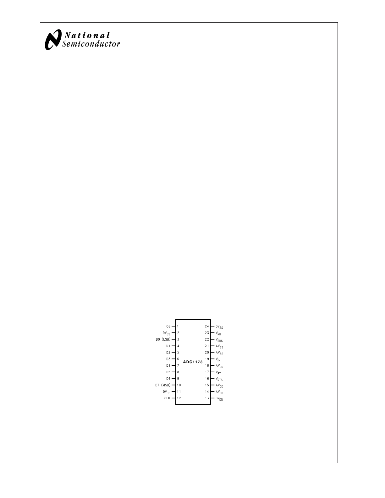
Pin Configuration
10089001
TRISTATE&®is a registered trademark of National Semiconductor Corporation.
© 2003 National Semiconductor Corporation DS100890 www.national.com
Page 2
Ordering Information
ADC1173
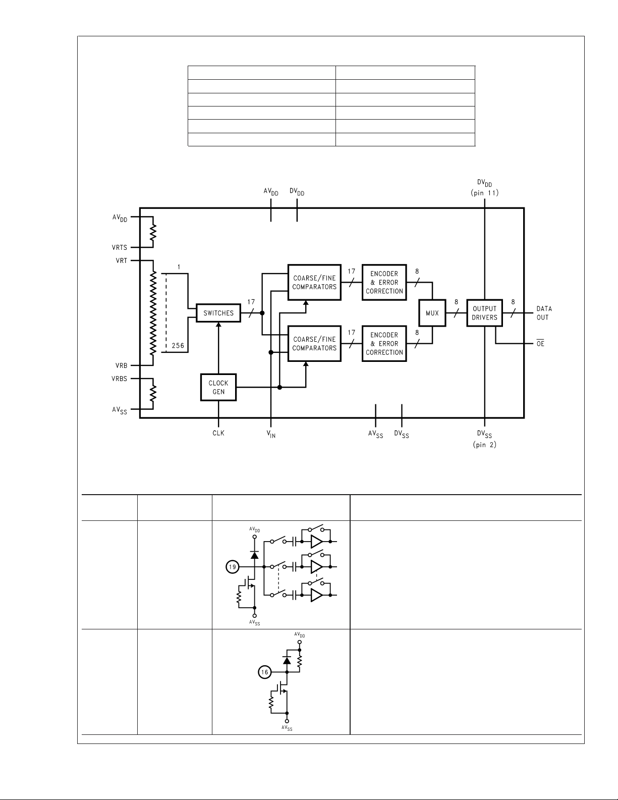
Block Diagram
Industrial (−40˚C ≤ TA≤ +75˚C) Package
ADC1173CIJM SOIC (EIAJ)
ADC1173CIJMX SOIC (EIAJ) (tape & reel)
ADC1173CIMTC TSSOP
ADC1173CIMTCX TSSOP (tape & reel)
ADC1173EVAL Evaluation Board
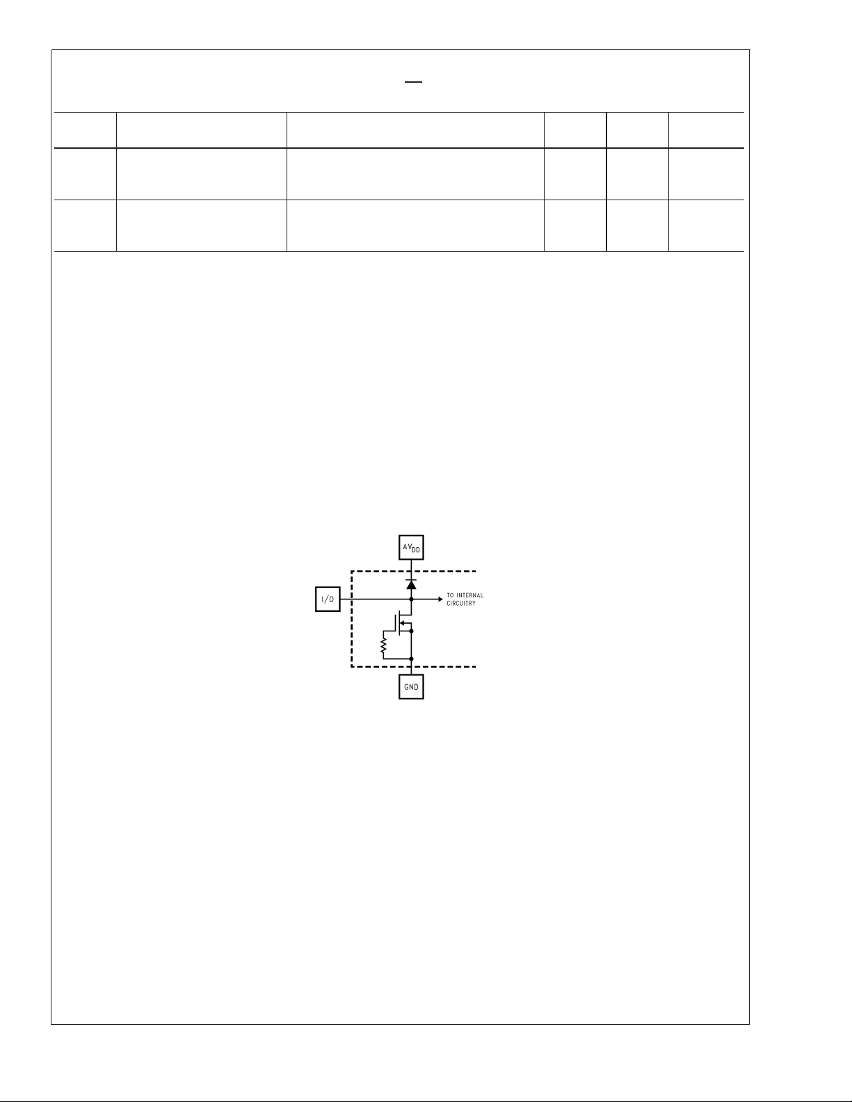
Pin Descriptions and Equivalent Circuits
Pin
No. Symbol Equivalent Circuit
19 V
16 V
IN
RTS
10089002
Description
Analog signal input. Conversion range is VRBto VRT.
Reference Top Bias with internal pull-up resistor.
Short this pin to V
to self bias the reference ladder.
RT
www.national.com 2
Page 3
Pin Descriptions and Equivalent Circuits (Continued)
ADC1173
Pin
No. Symbol Equivalent Circuit
17 V
23 V
22 V
RT
RB
RBS
1OE
Description
Analog Input that is the high (top) side of the
reference ladder of the ADC. Nominal range is 1.0V
to AV
V
. Voltage on VRTand VRBinputs define the
DD
conversion range. Bypass well. See Section 2.0
IN
for more information.
Analog Input that is the low (bottom) side of the
reference ladder of the ADC. Nominal range is 0V to
2.0V. Voltage on V
and VRBinputs define the V
RT
IN
conversion range. Bypass well. See Section 2.0 for
more information.
Reference Bottom Bias with internal pull down
resistor. Short to V
to self bias the reference
RB
ladder.
CMOS/TTL compatible Digital input that, when low,
enables the digital outputs of the ADC1173. When
high, the outputs are in a high impedance state.
12 CLK
3 thru
10
D0-D7
11, 13 DV
CMOS/TTL compatible digital clock Input. VINis
sampled on the falling edge of CLK input.
Conversion data digital Output pins. D0 is the LSB,
D7 is the MSB. Valid data is output just after the
rising edge of the CLK input. These pins are enabled
by bringing the OE pin low.
Positive digital supply pin. Connect to a clean, quiet
voltage source of +3V. AV
DD
a common source and be separately bypassed with a
and DVDDshould have
DD
10µF capacitor and a 0.1µF ceramic chip capacitor.
See Section 3.0 for more information.
www.national.com3
Page 4
Pin Descriptions and Equivalent Circuits (Continued)
Pin
ADC1173
No. Symbol Equivalent Circuit
2, 24 DV
14, 15,
18
20, 21 AV
AV
SS
DD
SS
Description
The ground return for the digital supply. AVSSand
should be connected together close to the
DV
SS
ADC1173.
Positive analog supply pin. Connected to a clean,
quiet voltage source of +3V. AV
and DVDDshould
DD
have a common source and be separately bypassed
with a 10 µF capacitor and a 0.1 µF ceramic chip
capacitor. See Section 3.0 for more information.
The ground return for the analog supply. AVSSand
should be connected together close to the
DV
SS
ADC1173 package.
www.national.com 4
Page 5
ADC1173
Absolute Maximum Ratings (Note 1)
If Military/Aerospace specified devices are required,
please contact the National Semiconductor Sales Office/
Distributors for availability and specifications.
,DV
AV
DD
DD
Voltage on Any Pin −0.3V to 6.5V
V
RT,VRB
CLK, OE Voltage −0.5 to (AVDD+ 0.5V)
Digital Output Voltage DV
Input Current (Note 3)
6.5V
AVDDto V
to DV
SS
±
25mA
SS
DD
Operating Ratings(Notes 1, 2)
Temperature Range −40˚C ≤ T
AV
,DV
DD
DD
|AV
-DVSS| 0V to 100 mV
SS
V
RT
V
RB
RT-RB
V
Voltage Range VRBto V
IN
+2.7V to +3.6V
≤ +75˚C
A
1.0V to AV
0V to 2.0V
1.0V to 2.8V
Package Input Current
±
(Note 3)
50mA
Package Dissipation at 25˚C (Note 4)
ESD Susceptibility (Note 5)
Human Body Model 2000V
Machine Model 200V
Soldering Temp., Infrared, 10
sec. (Note 6) 300˚C
Storage Temperature −65˚C to +150˚C
Converter Electrical Characteristics
The following specifications apply for AVDD=DVDD= +3.0VDC, OE = 0V, VRT= +2.0V, VRB= 0V, CL= 20 pF, f
at 50% duty cycle. Boldface limits apply for TA=T
Symbol Parameter Conditions
MIN
to T
; all other limits TA= 25˚C (Notes 7, 8)
MAX
Typical
(Note 9)
Limits Units
DC Accuracy
INL Integral Non Linearity
DNL Differential Non Linearity
±
0.5
±
0.4
±
1.3 LSB( max)
±
0.85 LSB( max)
Missing Codes 0 (max)
E
OT
E
OB
Top Offset −12 mV
Bottom Offset +1.0 mV
Video Accuracy
DP Differential Phase Error f
DG Differential Gain Error f
= 3.58 MHz sine wave 0.5 Degree
in
= 3.58 MHz sine wave 1.5 %
in
Analog Input and Reference Characteristics
V
V
IN
C
IN
R
IN
Input Range 2.0
VINInput Capacitance VIN= 1.5V + 0.7Vrms
Input Resistance
(CLK LOW) 4
(CLK HIGH) 11
>
1MΩ
RB
V
RT
BW Analog Input Bandwidth 120 MHz
R
R
R
I
RT
REF
RB
REF
Top Reference Resistor 360 Ω
Reference Ladder Resistance VRTto V
RB
300 200 Ω(min)
400 Ω(max)
Bottom Reference Resistor 90 Ω
V
RT=VRTS,VRB=VRBS
4.2
Reference Ladder Current
V
RT=VRTS,VRB
=AV
SS
4.8 mA
CLK
= 15MHz
V(min)
V(max)
pF
mA
DD
RT
V
RT
V
RB
Reference Top Self Bias
Voltage
Reference Bottom Self Bias
Voltage
VRTconnected to V
VRBconnected to V
connected to V
V
RT
V
connected to V
RB
RTS
RBS
RTS
RBS
1.56
0.36
1.45
1.65
0.32 V(min)
0.40 V(max)
V(min)
V(max)
www.national.com5
Page 6
Converter Electrical Characteristics (Continued)
The following specifications apply for AVDD=DVDD= +3.0VDC, OE = 0V, VRT= +2.0V, VRB= 0V, CL= 20 pF, f
at 50% duty cycle. Boldface limits apply for TA=T
ADC1173
Symbol Parameter Conditions
V
connected to V
RT
connected to V
V
RTS
V
RBS
V
RT-VRB
Self Bias Voltage Delta
Reference Voltage Delta 2
V
RB
V
connected to V
RT
connected to V
V
RB
Power Supply Characteristics
IA
ID
IAV
IDV
DD
DD
DD
DD
Analog Supply Current DVDD=AVDD= 3.6V 6.8 mA
Digital Supply Current DVDD=AVDD= 3.6V 2.3 mA
DV
+
Total Operating Current
DDAVDD
DV
=AVDD= 3.6V, CLK Low
DD
(Note 10)
Power Consumption DVDD=AVDD= 3.6V 33 41 mW
CLK, OE Digital Input Characteristics
V
IH
V
IL
I
IH
I
IL
C
IN
Logical High Input Voltage DVDD=AVDD= 3.6V 2.2 V (min)
Logical Low Input Voltage DVDD=AVDD= 3.6V 0.8 V (max)
Logical High Input Current VIH=DVDD=AVDD= 3.6V 5 µA
Logic Low Input Current VIL= 0V, DVDD=AVDD= 3.6V −5 µA
Logic Input Capacitance 5 pF
Digital Output Characteristics
= 2.7V, IOH= −360µA 2.4 V(min)
DV
V
V
I
I
OH
OL
OZH
OZL
High Level Output Voltage
Low Level Output Voltage DVDD= 2.7V, IOL= 1.6mA 0.32 0.6 V(max)
,
TRI-STATE®Leakage Current
DD
DV
= 2.7V, IOH= −1.1mA 2.1 1.9 V(min)
DD
DV
= 3.6V, OE = DVDD,
DD
V
OL
=0VorVOH=DV
AC Electrical Characteristics
f
C1
f
C2
t
−0 Output Delay CLK high to low data valid 28 ns(max)
OD
t
−1 Output Delay CLK low to high data valid 24 ns(max)
OD
Maximum Conversion Rate 20 15 MHz(min)
Minimum Conversion Rate 1 MHz
Pipeline Delay (Latency) 2.5
t
DS
t
AJ
t
OH
t
EN
t
DIS
ENOB Effective Number of Bits
SINAD Signal-to- Noise & Distortion
SNR Signal-to-Noise Ratio
Sampling (Aperture) Delay CLK low to acquisition of data 3 ns
Aperture Jitter 30 ps rms
Output Hold Time CLK high to data invalid 15 ns
OE Low to Data Valid Loaded as in Figure 2 22 ns
OE High to High Z State Loaded as in Figure 2 12 ns
f
= 1.31 MHz
IN
= 3.58 MHz
f
IN
= 7.5 MHz
f
IN
= 1.31 MHz
f
IN
= 3.58 MHz
f
IN
= 7.5 MHz
f
IN
= 1.31 MHz
f
IN
= 3.58 MHz
f
IN
= 7.5 MHz
f
IN
MIN
to T
; all other limits TA= 25˚C (Notes 7, 8)
MAX
Typical
(Note 9)
,
RTS
RBS
,
RTS
SS
Limits Units
1.2
1.1
1.3
1.38 V
1.0 V(min)
V
A
= 3.6V, 9.1 11.4 mA
5.8 mA
±
20 µA
DD
7.7
7.6
7.0 Bits (min)
7.4
49
47.7
43 dB(min)
46.5
49
48.7
44 dB(min)
48.0
CLK
= 15MHz
µAmin
µAmax
V(max)
Clock
Cycles
www.national.com 6
Page 7
Converter Electrical Characteristics (Continued)
The following specifications apply for AVDD=DVDD= +3.0VDC, OE = 0V, VRT= +2.0V, VRB= 0V, CL= 20 pF, f
at 50% duty cycle. Boldface limits apply for TA=T
Symbol Parameter Conditions
= 1.31 MHz
f
IN
= 3.58 MHz
SFDR Spurious Free Dynamic Range
THD Total Harmonic Distortion
Note 1: Absolute Maximum Ratings indicate limits beyond which damage to the device may occur. Operating Ratings indicate conditions for which the device is
functional, but do not guarantee specific performance limits. For guaranteed specifications and test conditions, see the Electrical Characteristics. The guaranteed
specifications apply only for the test conditions listed. Some performance characteristics may degrade when the device is not operated under the listed test
conditions.
Note 2: All voltages are measured with respect to GND = AV
Note 3: When the input voltage at any pin exceeds the power supplies (that is, less than AV
be limited to 25 mA. The 50 mA maximum package input current rating limits the number of pins that can safely exceed the power supplies with an input current of
25 mA to two.
Note 4: The absolute maximum junction temperatures (T
junction-to-ambient thermal resistance θ
TSSOP, θ
this part is 98˚C/W for the EIAJ SOIC). Note that the power dissipation of this device under normal operation will typically be about 49 mW (33 mW quiescent power
+ 13 mW reference ladder power+3mWdueto1TTLloan on each digital output. The values for maximum power dissipation listed above will be reached only when
the ADC1173 is operated in a severe fault condition (e.g. when input or output pins are driven beyond the power supply voltages, or the power supply polarity is
reversed). Obviously, such conditions should always be avoided.
Note 5: Human body model is 100 pF capacitor discharged through a 1.5kΩ resistor. Machine model is 220 pf discharged through ZERO Ω.
Note 6: See AN450, "Surface Mounting Methods and Their Effect on Product Reliability", or the section entitled "Surface Mount" found in any post 1986 National
Semiconductor Linear Data Book, for other methods of soldering surface mount devices.
Note 7: The analog inputs are protected as shown below. Input voltage magnitudes up to 6.5V or to 500 mV below GND will not damage this device. However, errors
in the A/D conversion can occur if the input goes above V
be ≤2.75V
is 92˚C/W, so PDMAX = 1,358 mW at 25˚C and 815 mW at the maximum operating ambient temperature of 75˚C. (Typical thermal resistance, θJA,of
JA
to ensure accurate conversions.
DC
, and the ambient temperature, TA, and can be calculated using the formula PDMAX=(TJmax - TA)/θJA. In the 24-pin
JA
f
IN
= 7.5 MHz
f
IN
= 1.31 MHz
f
IN
= 3.58 MHz
f
IN
= 7.5 MHz
f
IN
SS
max) for this device is 150˚C. The maximum allowable power dissipation is dictated by TJmax, the
J
or below GND by more than 50 mV. As an example, if AVDDis 2.7VDC, the full-scale input voltage must
DD
to T
MIN
=DVSS= 0V, unless otherwise specified.
; all other limits TA= 25˚C (Notes 7, 8)
MAX
or DVSS, or greater than AVDDor DVDD), the current at that pin should
SS
Typical
(Note 9)
65
55
51
−62
−54
−51
Limits Units
CLK
= 15MHz
ADC1173
dB
dB
10089010
Note 8: To guarantee accuracy, it is required that AVDDand DVDDbe well bypassed. Each supply pin must be decoupled with separate bypass capacitors.
Note 9: Typical figures are at T
Level).
Note 10: At least two clock cycles must be presented to the ADC1173 after power up. See Section 4.0 for details.
= 25˚C, and represent most likely parametric norms. Test limits are guaranteed to National’s AOQL (Average Outgoing Quality
J
www.national.com7
Page 8

Typical Performance Characteristics
ADC1173
INL vs Temperature DNL vs Temperature
10089020 10089021
SNR vs Temperature SNR vs f
IN
10089022
THD vs Temperature SINAD vs Temperature
10089023
www.national.com 8
10089033
10089034
Page 9

Typical Performance Characteristics (Continued)
ADC1173
SINAD vs f
SFDR vs f
IN
10089031
IN
SFDR vs Temperature
10089035
Differential Gain vs Temperature
10089029
Differential Phase vs Temperature SNR vs f
10089027
10089026
IN
10089036
www.national.com9
Page 10

Typical Performance Characteristics (Continued)
ADC1173
THD vs f
SFDR vs f
IN
10089037
IN
SINAD vs f
IN
SNR vs SUPPLY VOLTAGE
10089038
10089039 10089040
THD vs SUPPLY VOLTAGE SINAD vs SUPPLY VOLTAGE
10089041 10089042
www.national.com 10
Page 11

Typical Performance Characteristics (Continued)
ADC1173
SFDR vs SUPPLY VOLTAGE ID
10089043
+IADDvs f
DD
TODvs Temperature Spectral Response
CLK
10089032
10089025
10089028
www.national.com11
Page 12

Specification Definitions
ANALOG INPUT BANDWIDTH is a measure of the fre-
ADC1173
quency at which the reconstructed output fundamental drops
3 dB below its low frequency value for a full scale input. The
test is performed with f
multiples of f
. The input frequency at which the output is
CLK
−3 dB relative to the low frequency input signal is the full
power bandwidth.
APERTURE JITTER is the time uncertainty of the sampling
point (t
), or the range of variation in the sampling delay.
DS
BOTTOM OFFSET is the difference between the input voltage that just causes the output code to transition to the first
code and the negative reference voltage. Bottom offset is
defined as E
=VZT-VRB, where VZTis the first code
OB
transition input voltage. Note that this is different from the
normal Zero Scale Error.
DIFFERENTIAL GAIN ERROR is the percentage difference
between the output amplitudes of a high frequency reconstructed sine wave at two different dc levels.
DIFFERENTIAL NON-LINEARITY (DNL) is the measure of
the maximum deviation from the ideal step size of 1 LSB.
DIFFERENTIAL PHASE ERROR is the difference in the
output phase of a reconstructed small signal sine wave at
two different dc levels.
EFFECTIVE NUMBER OF BITS (ENOB, or EFFECTIVE
BITS) is another method of specifying Signal-to-Noise and
Distortion Ratio, or SINAD. ENOB is defined as (SINAD -
1.76) / 6.02 and says that the converter is equivalent to a
perfect ADC of this (ENOB) number of bits.
INTEGRAL NON-LINEARITY (INL) is a measure of the
deviation of each individual code from a line drawn from zero
1
⁄2LSB below the first code transition) through positive
scale (
full scale (
1
⁄2LSB above the last code transition). The deviation of any given code from this straight line is measured
from the center of that code value. The end point test method
is used.
OUTPUT DELAY is the time delay after the rising edge of
the input clock before the data update is present at the
output pins.
equal to 100 kHz plus integer
IN
OUTPUT HOLD TIME is the length of time that the output
data is valid after the rise of the input clock.
PIPELINE DELAY (LATENCY) is the number of clock cycles
between initiation of conversion and the availability of that
conversion result at the output. New data is available at
every clock cycle, but the data lags the conversion by the
pipeline delay.
SAMPLING (APERTURE) DELAY is that time required after
the fall of the clock input for the sampling switch to open. The
Sample/Hold circuit effectively stops capturing the input signal and goes into the "hold" mode t
after the clock goes
DS
low.
SIGNAL TO NOISE RATIO (SNR) is the ratio of the rms
value of the input signal to the rms value of the other spectral
components below one-half the sampling frequency, not including harmonics or dc.
SIGNAL TO NOISE PLUS DISTORTION (S/(N+D) or SINAD) Is the ratio of the rms value of the input signal to the
rms value of all of the other spectral components below half
the clock frequency, including harmonics but excluding dc.
SPURIOUS FREE DYNAMIC RANGE (SFDR) is the difference, expressed in dB, between the rms values of the input
signal and the peak spurious signal, where a spurious signal
is any signal present in the output spectrum that is not
present at the input.
TOP OFFSET is the difference between the positive reference voltage and the input voltage that just causes the
output code to transition to full scale and is defined as E
V
FT−VRT
. Where VFTis the full scale transition input volt-
OT
age. Note that this is different from the normal Full Scale
Error.
TOTAL HARMONIC DISTORTION (THD) is the ratio of the
rms total of the first six harmonic components, to the rms
value of the input signal.
=
www.national.com 12
Page 13

Timing Diagram
ADC1173
FIGURE 1. ADC1173 Timing Diagram
10089012
FIGURE 2. tEN,t
Test Circuit
DIS
10089011
www.national.com13
Page 14

Functional Description
The ADC1173 uses a new, unique architecture to achieve
ADC1173
7.4 effective bits at and maintains superior dynamic performance up to
The analog signal at V
by V
RT
Input voltages below V
consist of all zeroes. Input voltages above V
output word to consist of all ones. V
to the analog supply voltage, AV
0 to 2.0 Volts. V
positive than V
If V
RT
1
⁄2the clock frequency.
that is within the voltage range set
IN
and VRBare digitized to eight bits at up to 20 MSPS.
will cause the output word to
RB
RT
has a range of 1.0 Volt
RT
, while VRBhas a range of
DD
and V
should always be at least 1.0 Volt more
RT
.
RB
are connected together and VRBand V
RTS
are connected together, the nominal values of VRTand V
are 1.56V and 0.36V, respectively. If VRTand V
connected together and V
is 1.38V.
of V
RT
is grounded, the nominal value
RB
Data is acquired at the falling edge of the clock and the
digital equivalent of the data is available at the digital outputs
2.5 clock cycles plus t
later. The ADC1173 will convert as
OD
long as the clock signal is present at pin 12. The Output
Enable pin OE, when low, enables the output pins. The
digital outputs are in the high impedance state when the OE
pin is high.
Applications Information
1.0 THE ANALOG INPUT
The analog input of the ADC1173 is a switch followed by an
integrator. The input capacitance changes with the clock
level, appearing as 4 pF when the clock is low, and 11 pF
when the clock is high. Since a dynamic capacitance is more
difficult to drive than a fixed capacitance, choose an amplifier
that can drive this type of load. The LMH6702, LM6152,
LM6154, LM6181 and LM6182 have been found to be excellent devices for driving the ADC1173. Do not drive the
input beyond the supply rails.
will cause the
RBS
RB
are
RTS
Figure 3 shows an example of an input circuit using the
LM6181. This circuit has both gain and offset adjustments. If
you desire to eliminate these adjustments, you should reduce the signal swing to avoid clipping at the ADC1173
output that can result from normal tolerances of all system
components. With no adjustments, the nominal value for the
amplifier feedback resistor is 510Ω and the 5.1k resistor at
the inverting input should be changed to 860Ω and returned
to +3V rather than to the Offset Adjust potentiometer.
Driving the analog input with input signals up to 2.8V
result in normal behavior where voltages above V
result in a code of FFh and input voltages below V
result in an output code of zero. Input signals above 2.8V
P-P
RT
RB
will
will
will
P-P
may result in odd behavior where the output code is not FFh
when the input exceeds V
.
RT
2.0 REFERENCE INPUTS
The reference inputs V
(Reference Top) and VRB(Refer-
RT
ence Bottom) are the top and bottom of the reference ladder.
Input signals between these two voltages will be digitized to
8 bits. External voltages applied to the reference input pins
should be within the range specified in the Operating Ratings
table (1.0V to AV
for VRTand 0V to (AVDD- 1.0V) for VRB).
DD
Any device used to drive the reference pins should be able to
source sufficient current into the V
current from the V
pin.
RB
The reference ladder can be self-biased by connecting V
to V
and connecting VRBto V
RTS
pin and sink sufficient
RT
to provide top and
RBS
RT
bottom reference voltages of approximately 1.56V and
0.36V, respectively, with V
shown in Figure 3.IfV
RT
= 3.0V. This connection is
CC
and V
are tied together, but V
RTS
RB
is tied to analog ground, a top reference voltage of approximately 1.38V is generated. The top and bottom of the ladder
should be bypassed with 10µF tantalum capacitors located
close to the reference pins.
www.national.com 14
Page 15

Applications Information (Continued)
ADC1173
10089013
FIGURE 3. Simple, Low Component Count, Self -Bias Reference application. Because of resistor tolerances, the
reference voltages can vary by as much as 6%. Choose an amplifier that can drive a dynamic capacitance (see text).
The reference self-bias circuit of Figure 3 is very simple and
performance is adequate for many applications. Superior
performance can generally be achieved by driving the reference pins with a low impedance source.
By forcing a little current into or out of the top and bottom of
the ladder, as shown in Figure 4, the top and bottom reference voltages can be trimmed. The resistive divider at the
amplifier inputs can be replaced with potentiometers. The
LMC662 amplifier shown was chosen for its low offset voltage and low cost. Note that a negative power supply is
needed for these amplifiers as their outputs may be required
to go slightly negative to force the required reference
voltages.
www.national.com15
Page 16

Applications Information (Continued)
ADC1173
10089014
FIGURE 4. Better defining the ADC Reference Voltage. Self-bias is still used, but the reference voltages are trimmed
by providing a small trim current with the operational amplifiers.
10089015
FIGURE 5. Driving the reference to force desired values requires driving with a low impedance source, provided by
the transistors. Note that pins 16 and 22 are not connected.
www.national.com 16
Page 17

Applications Information (Continued)
If reference voltages are desired that are more than a few
tens of millivolts from the self-bias values, the circuit of
Figure 5 will allow forcing the reference voltages to whatever
levels are desired. This circuit provides the best performance
because of the low source impedance of the transistors.
Note that the V
can be anywhere between VRB+ 1.0V and the analog
V
RT
RTS
and V
supply voltage, and V
and 1.0V below V
. To minimize noise effects and ensure
RT
accurate conversions, the total reference voltage range (V
-VRB) should be a minimum of 1.0V and a maximum of
about V
and V
. Best performance can be realized with VRT= 1.56
A
= 0.36V.
RB
3.0 POWER SUPPLY CONSIDERATIONS
Many A/D converters draw sufficient transient current to
corrupt their own power supplies if not adequately bypassed.
A 10µF tantalum or aluminum electrolytic capacitor should
be placed within an of inch (2.5 centimeters) of the A/D
power pins, with a 0.1 µF ceramic chip capacitor placed as
close as possible to the converter’s power supply pins. Leadless chip capacitors are preferred because they have low
lead inductance.
While a single voltage source should be used for the analog
and digital supplies of the ADC1173, these supply pins
should be well isolated from each other to prevent any digital
noise from being coupled to the analog power pins. A 47
Ohm resistor is recommend between the analog and digital
supply lines, with a ceramic capacitor close to the analog
supply pin. Avoid inductive components in the analog supply
line.
The converter digital supply should not be the supply that is
used for other digital circuitry on the board. It should be the
same supply used for the A/D analog supply.
As is the case with all high speed converters, the ADC1173
should be assumed to have little power supply rejection,
especially when self-biasing is used by connecting V
together.
V
RTS
No pin should ever have a voltage on it that is in excess of
the supply voltages or below ground, not even on a transient
basis. This can be a problem upon application of power to a
circuit. Be sure that the supplies to circuits driving the CLK,
OE, analog input and reference pins do not come up any
faster than does the voltage at the ADC1173 power pins.
4.0 THE ADC1173 CLOCK
Although the ADC1173 is tested and its performance is
guaranteed with a 15MHz clock, it typically will function with
clock frequencies from 1MHz to 20MHz.
If continuous conversions are not required, power consumption can be reduced somewhat by stopping the clock at a
logic low when the ADC1173 is not being used. This reduces
the current drain in the ADC1173’s digital circuitry from a
typical value of 2.3mA to about 100µA.
Note that powering up the ADC1173 with the clock stopped
may not save power, as it will result in an increased current
flow (by as much as 170%) in the reference ladder. In some
cases, this may increase the ladder current above the specified limit. Toggling the clock twice at 1MHz or higher and
returning it to the low state will eliminate the excess ladder
current.
pins are left floating.
RBS
can be anywhere between ground
RB
RT
and
RT
ADC1173
An alternative power-saving technique is to power up the
ADC1173 with the clock active, then halt the clock in the low
state after two clock cycles. Stopping the clock in the high
state is not recommended as a power-saving technique.
5.0 LAYOUT AND GROUNDING
Proper grounding and proper routing of all signals is essential to ensure accurate conversion. Separate analog and
digital ground planes that are connected beneath the
ADC1173 are required to meet data sheet limits. The analog
and digital grounds may be in the same layer, but should be
separated from each other. The analog and digital ground
planes should never overlap each other.
Capacitive coupling between the typically noisy digital
ground plane and the sensitive analog circuitry can lead to
poor performance that may seem impossible to isolate and
remedy. The solution is to keep the analog circuity well
separated from the digital circuitry and from the digital
ground plane.
Digital circuits create substantial supply and ground transients. The logic noise thus generated could have significant
impact upon system noise performance. The best logic family to use in systems with A/D converters is one which
employs non-saturating transistor designs, or has low noise
characteristics, such as the 74HC(T) and 74AC(T)Q families.
Worst noise generators are logic families that draw the largest supply current transients during clock or signal edges,
like the 74F and the 74AC(T) families. In general, slower
logic families, such as 74LS and 74HC(T), will produce less
high frequency noise than do high speed logic families, such
as the 74F and 74AC(T) families.
Since digital switching transients are composed largely of
high frequency components, total ground plane copper
weight will have little effect upon the logic-generated noise.
This is because of the skin effect. Total surface area is more
important than is total ground plane volume.
An effective way to control ground noise is by connecting the
analog and digital ground planes together beneath the ADC
with a copper trace that is very narrow (about 3/16 inch)
compared with the rest of the ground plane. This narrowing
beneath the converter provides a fairly high impedance to
the high frequency components of the digital switching currents, directing them away from the analog pins. The relatively lower frequency analog ground currents do not see a
significant impedance across this narrow ground connection.
Generally, analog and digital lines should cross each other at
90 degrees to avoid getting digital noise into the analog path.
In video (high frequency) systems, however, avoid crossing
analog and digital lines altogether. Clock lines should be
isolated from ALL other lines, analog and digital. Even the
generally accepted 90 degree crossing should be avoided as
even a little coupling can cause problems at high frequencies. Best performance at high frequencies and at high
resolution is obtained with a straight signal path.
Be especially careful with the layout of inductors. Mutual
inductance can change the characteristics of the circuit in
which they are used. Inductors should not be placed side by
side, not even with just a small part of their bodies being
beside each other.
The analog input should be isolated from noisy signal traces
to avoid coupling of spurious signals into the input. Any
external component (e.g., a filter capacitor) connected between the converter’s input and ground should be connected
to a very clean point in the analog ground return.
www.national.com17
Page 18

Applications Information (Continued)
ADC1173
FIGURE 6. Layout example showing separate analog
and digital ground planes connected below the
ADC1173.
Figure 6 gives an example of a suitable layout. All analog
circuitry (input amplifiers, filters, reference components, etc.)
should be placed on or over the analog ground plane. All
digital circuitry and I/O lines should be placed over the digital
ground plane.
6.0 DYNAMIC PERFORMANCE
The ADC1173 is ac tested and its dynamic performance is
guaranteed. To meet the published specifications, the clock
source driving the CLK input must be free of jitter. For best
ac performance, isolating the ADC clock from any digital
circuitry should be done with adequate buffers, as with a
clock tree. See Figure 7.
FIGURE 7. Isolating the ADC clock from Digital
Circuitry.
10089017
10089016
7.0 COMMON APPLICATION PITFALLS Driving the inputs (analog or digital) beyond the power
supply rails. For proper operation, all inputs should not go
more than 50mV below the ground pins or 50mV above the
supply pins. Exceeding these limits on even a transient basis
can cause faulty or erratic operation. It is not uncommon for
high speed digital circuits (e.g., 74F and 74AC devices) to
exhibit undershoot that goes more than a volt below ground.
A resistor of 50Ω in series with the offending digital input will
usually eliminate the problem.
Care should be taken not to overdrive the inputs of the
ADC1173. Such practice may lead to conversion inaccuracies and even to device damage.
Attempting to drive a high capacitance digital data bus.
The more capacitance the output drivers must charge for
each conversion, the more instantaneous digital current is
required from DV
and DGND. These large charging cur-
DD
rent spikes can couple into the analog section, degrading
dynamic performance. Buffering the digital data outputs (with
an 74ACQ541, for example) may be necessary if the data
bus to be driven is heavily loaded. Dynamic performance
can also be improved by adding 47Ω series resistors at each
digital output, reducing the energy coupled back into the
converter output pins.
Using an inadequate amplifier to drive the analog input.
As explained in Section 1.0, the capacitance seen at the
input alternates between 4 pF and 11 pF with the clock. This
dynamic capacitance is more difficult to drive than is a fixed
capacitance, and should be considered when choosing a
driving device. The LMH6702, LM6152, LM6154, LM6181
and LM6182 have been found to be excellent devices for
driving the ADC1173 analog input.
Driving the V
pin or the VRBpin with devices that can
RT
not source or sink the current required by the ladder. As
mentioned in section 2.0, care should be taken to see that
any driving devices can source sufficient current into the V
RT
pin and sink sufficient current from the VRBpin. If these pins
are not driven with devices than can handle the required
current, these reference pins will not be stable, resulting in a
reduction of dynamic performance.
Using a clock source with excessive jitter, using an
excessively long clock signal trace, or having other
signals coupled to the clock signal trace. This will cause
the sampling interval to vary, causing excessive output noise
and a reduction in SNR performance. Simple gates with RC
timing is generally inadequate as a clock source.
Input test signal contains harmonic distortion that interferes with the measurement of dynamic signal to noise
ratio. Harmonic and other interfering signals can be re-
moved by inserting a filter at the signal input. Suitable filters
are shown in Figure 8 and Figure 9. The circuit of Figure 8
has cutoff of about 5.5 MHz and is suitable for input frequencies of 1 MHz to 5 MHz. The circuit of Figure 9 has a cutoff
of about 11 MHz and is suitable for input frequencies of 5
MHz to 10 MHz. These filters should be driven by a generator of 75 Ohm source impedance and terminated with a 75
ohm resistor.
It is good practice to keep the ADC clock line as short as
possible and to keep it well away from any other signals.
Other signals can introduce jitter into the clock signal.
www.national.com 18
Page 19

Applications Information (Continued)
FIGURE 8. 5.5 MHz Low Pass Filter to Eliminate Harmonics at the Signal Input.
FIGURE 9. 11 MHz Low Pass filter to eliminate harmonics at the signal input.
Use at input frequencies of 5 MHz to 10 MHz
ADC1173
10089018
10089019
www.national.com19
Page 20

Physical Dimensions inches (millimeters) unless otherwise noted
ADC1173
24-Lead Package JM
Ordering Number ADC1173CIJM
NS Package Number M24D
www.national.com 20
Page 21

Physical Dimensions inches (millimeters) unless otherwise noted (Continued)
ADC1173 8-Bit, 3-Volt, 15MSPS, 33mW A/D Converter
24-Lead Package TC
Ordering Number ADC1173CIMTC
NS Package Number MTC24
LIFE SUPPORT POLICY
NATIONAL’S PRODUCTS ARE NOT AUTHORIZED FOR USE AS CRITICAL COMPONENTS IN LIFE SUPPORT
DEVICES OR SYSTEMS WITHOUT THE EXPRESS WRITTEN APPROVAL OF THE PRESIDENT AND GENERAL
COUNSEL OF NATIONAL SEMICONDUCTOR CORPORATION. As used herein:
1. Life support devices or systems are devices or
systems which, (a) are intended for surgical implant
into the body, or (b) support or sustain life, and
whose failure to perform when properly used in
accordance with instructions for use provided in the
2. A critical component is any component of a life
support device or system whose failure to perform
can be reasonably expected to cause the failure of
the life support device or system, or to affect its
safety or effectiveness.
labeling, can be reasonably expected to result in a
significant injury to the user.
National Semiconductor
Americas Customer
Support Center
Email: new.feedback@nsc.com
Tel: 1-800-272-9959
www.national.com
National does not assume any responsibility for use of any circuitry described, no circuit patent licenses are implied and National reserves the right at any time without notice to change said circuitry and specifications.
National Semiconductor
Europe Customer Support Center
Fax: +49 (0) 180-530 85 86
Email: europe.support@nsc.com
Deutsch Tel: +49 (0) 69 9508 6208
English Tel: +44 (0) 870 24 0 2171
Français Tel: +33 (0) 1 41 91 8790
National Semiconductor
Asia Pacific Customer
Support Center
Fax: +65-6250 4466
Email: ap.support@nsc.com
Tel: +65-6254 4466
National Semiconductor
Japan Customer Support Center
Fax: 81-3-5639-7507
Email: jpn.feedback@nsc.com
Tel: 81-3-5639-7560
 Loading...