

Page 1

ADC10D020
Dual 10-Bit, 20 MSPS, 150 mW A/D Converter
ADC10D020 Dual 10-Bit, 20 MSPS, 150 mW A/D Converter
April 2002
General Description
The ADC10D020 is a dual low power, high performance
CMOS analog-to-digital converter that digitizes signals to 10
bits resolution at sampling rates up to 30 MSPS while consuming a typical 150 mW from a single 3.0V supply. No
missing codesisguaranteed over the full operating temperature range. The unique two stage architecture achieves 9.5
Effective Bits over the entire Nyquist band at 20 MHz sample
rate. An output formatting choice of straight binary or 2’s
complement coding and a choice of two gain settings eases
the interface to many systems. Also allowing great flexibility
of use is a selectable 10-bit multiplexed or 20-bit parallel
output mode. An offset correction feature minimizes the offset error.
To ease interfacing to most low voltage systems, the digital
output power pins of the ADC10D020 can be tied to a
separate supply voltage of 1.5V to 3.6V, making the outputs
compatible with other low voltage systems. When not converting, power consumption can be reduced by pulling the
PD (Power Down) pin high, placing the converter into a low
power state where it typically consumes less than 1 mW and
from which recovery is less than 1 ms. Bringing the STBY
(Standby) pin high places the converter into a standby mode
where power consumption is about 27 mW and from which
recovery is 800 ns.
The ADC10D020’s speed, resolution and single supply operation makes it well suited for a variety of applications,
including high speed portable applications.
Operating over the industrial (−40˚ ≤ T
ture range, theADC10D020 is available in a 48-pinTQFP.An
evaluation board is available to ease the design effort.
≤ +85˚C) tempera-
A
Features
n Internal sample-and-hold
n Internal reference capability
n Dual gain settings
n Offset correction
n Selectable straight binary or 2’s complement output
n Multiplexed or parallel output bus
n Single +2.7V to 3.6V operation
n Power down and standby modes
Key Specifications
n Resolution 10 Bits
n Conversion Rate 20 MSPS
n ENOB 9.5 Bits (typ)
n DNL 0.35 LSB (typ)
n Conversion Latency Parallel Outputs 2.5 Clock Cycles
— Multiplexed Outputs, I Data Bus 2.5 Clock Cycles
— Multiplexed Outputs, Q Data Bus 3 Clock Cycles
n PSRR 90 dB
n Power Consumption—Normal Operation 150 mW (typ)
— Power Down Mode
— Fast Recovery Standby Mode 27 mW (typ)
<
1 mW (typ)
Applications
n Digital Video
n CCD Imaging
n Portable Instrumentation
n Communications
n Medical Imaging
n Ultrasound
© 2002 National Semiconductor Corporation DS200255 www.national.com
Page 2
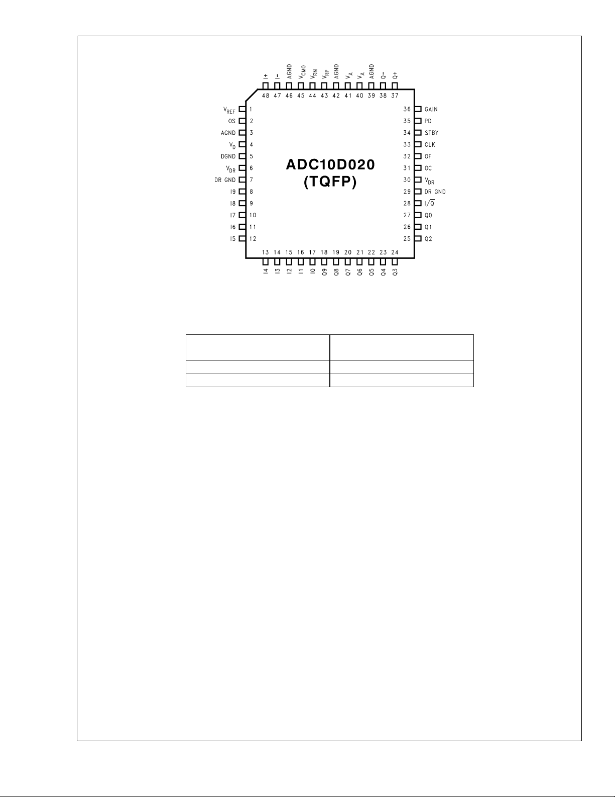
Connection Diagram
ADC10D020
Ordering Information
Industrial Temperature Range
TOP VIEW
(−40˚C ≤ T
ADC10D020CIVS TQFP
ADC10D020EVAL Evaluation Board
≤ +85˚C)
A
NS Package
20025501
www.national.com 2
Page 3
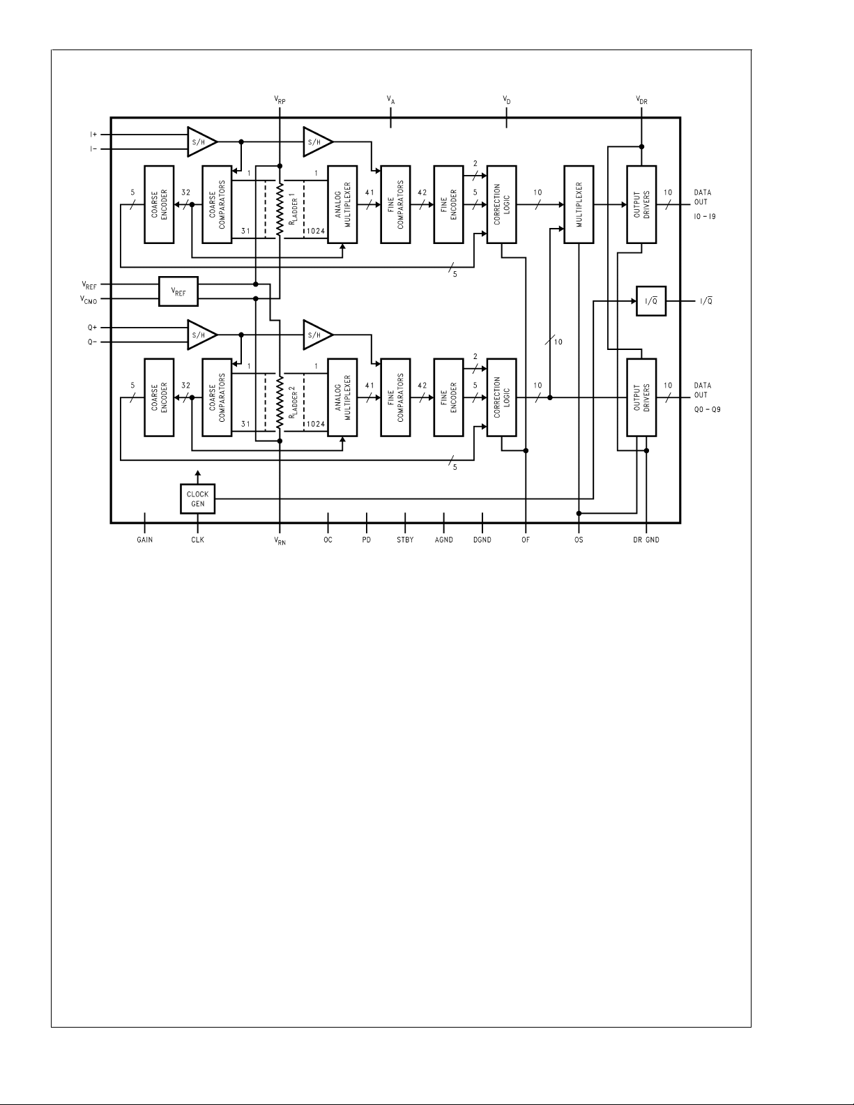
Block Diagram
ADC10D020
20025502
www.national.com3
Page 4
Pin Descriptions and Equivalent Circuits
Pin No. Symbol Equivalent Circuit Description
ADC10D020
48
47
I+
I−
Analog inputs to “I” ADC. Nominal conversion range is 1.25V
to 1.75V with GAIN pin low, or 1.0V to 2.0V with GAIN pin
high.
37
38
1V
45 V
43 V
Q+
Q−
REF
CMO
RP
Analog inputs to “Q” ADC. Nominal conversion range is 1.25V
to 1.75V with GAIN pin low, or 1.0V to 2.0V with GAIN pin
high.
Analog Reference Voltage input. The voltage at this pin
should be in the range of 0.8V to 1.5V. With 1.0V at this pin
low
and the GAIN pin
. With 1.0V at this pin and the GAIN pin
1V
P-P
scale differential inputs are 2 V
, the full scale differential inputs are
high
, the full
. This pin should be
P-P
bypassed with a minimum 1 µF capacitor.
This is an analog output which can be used as a reference
source and/or to set the common mode voltage of the input. It
should be bypassed with a minimum of 1 µF low ESR
capacitor in parallel with a 0.1 µF capacitor. This pin has a
nominal output voltage of 1.5V and hasa1mAoutput source
capability.
Top of the reference ladder. Do not drive this pin. Bypass
this pin with a 10 µF low ESR capacitor and a 0.1 µF
capacitor.
44 V
www.national.com 4
RN
Bottom of the reference ladder. Do not drive this pin.
Bypass this pin with a 10 µF low ESR capacitor and a 0.1 µF
capacitor.
Page 5
Pin Descriptions and Equivalent Circuits (Continued)
Pin No. Symbol Equivalent Circuit Description
33 CLK
2OS
31 OC
32 OF
34 STBY
35 PD
36 GAIN
8 thru 27 I0–I9 and Q0–Q9
28 I/Q
40, 41 V
A
Digital clock input for both converters. The analog inputs are
sampled on the falling edge of this clock input.
Output Bus Select. With this pin at a logic high, both the “I”
and the “Q” data are present on their respective 10-bit output
buses (Parallel mode of operation). When this pin is at a logic
low, the “I” and “Q” data are multiplexed onto the “I” output
bus and the “Q” output lines all remain at a logic low
(multiplexed mode).
Offset Correct pin. A low-to-high transition on this pin initiates
an independent offset correction sequence for each converter,
which takes 34 clock cycles to complete. During this time 32
conversions are taken and averaged. The result is subtracted
from subsequent conversions. Each input pair should have 0V
differential value during this entire 34 clock period.
Output Format pin. When this pin is LOW the output format is
Straight Binary. When this pin is HIGH the output format is 2’s
complement. This pin may be changed asynchronously, but
this will result in errors for one or two conversions.
Standby pin. The device operates normally with a logic low on
this and the PD (Power Down) pin. With this pin at a logic
high and the PD pin at a logic low, the device is in the
standby mode where it consumes just 27 mW of power. It
takes just 800 ns to come out of this mode after the STBY pin
is brought low.
Power Down pin that, when high, puts the converter into the
Power Down mode where it consumes less than 1 mW of
power. It takes less than 1 ms to recover from this mode after
the PD pin is brought low. If both the STBY and PD pins are
high simultaneously, the PD pin dominates.
This pin sets the internal signal gain at the inputs to the
ADCs. With this pin low the full scale differential input
peak-to-peak signal is equal to V
REF
full scale differential input peak-to-peak signal is equal to 2 x
.
V
REF
3V TTL/CMOS-compatible Digital Output pins that provide the
conversion results of the I and Q inputs. I0 and Q0 are the
LSBs, I9 and Q9 are the MSBs. Valid data is present just after
the rising edge of the CLK input in the Parallel mode. In the
multiplexed mode, I-channel data is valid on I0 through I9
when the I/Q output is high and the Q-channel data is valid
on I0 through I9 when the I/Q output is low.
Output data valid signal. In the multiplexed mode, this pin
transitions from low to high when the data bus transitions
from Q-data to I-data, and from high to low when the data bus
transitions from I-data to Q-data. In the Parallel mode, this pin
transitions from low to high as the output data changes.
Positive analog supply pin. This pin should be connected to a
quiet voltage source of +2.7V to +3.6V. V
have a common supply and be separately bypassed with
10 µF to 50 µF capacitors in parallel with 0.1 µF capacitors.
. With this pin high the
and VDshould
A
ADC10D020
www.national.com5
Page 6
Pin Descriptions and Equivalent Circuits (Continued)
Pin No. Symbol Equivalent Circuit Description
ADC10D020
4V
6, 30 V
3, 39, 42,
46
5 DGND
7, 29 DR GND The ground return of the digital output drivers.
D
DR
AGND
Digital supply pin. This pin should be connected to a quiet
voltage source of +2.7V to +3.6V. V
common supply and be separately bypassed with 10 µF to 50
µF capacitors in parallel with 0.1 µF capacitors.
Digital output driver supply pins. These pins should be
connected to a voltage source of +1.5V to V
bypassed with 10 µF to 50 µF capacitors in parallel with 0.1
µF capacitors.
The ground return for the analog supply. AGND and DGND
should be connected together close to the ADC10D020
package.
The ground return for the digital supply. AGND and DGND
should be connected together close to the ADC10D020
package.
and VDshould have a
A
and be
D
www.national.com 6
Page 7
ADC10D020
Absolute Maximum Ratings (Notes 1,
2)
If Military/Aerospace specified devices are required,
please contact the National Semiconductor Sales Office/
Distributors for availability and specifications.
Positive Supply Voltages 3.8V
Voltage on Any Pin −0.3V to (V
Input Current at Any Pin (Note 3)
Package Input Current (Note 3)
Package Dissipation at T
= 25˚C See (Note 4)
A
ESD Susceptibility (Note 5)
Human Body Model 2500V
Machine Model 250V
or VD+0.3V)
A
±
25 mA
±
50 mA
Operating Ratings (Notes 1, 2)
Operating Temperature Range −40˚C ≤ T
V
Supply Voltage +2.7V to +3.6V
A,VD
V
Supply Voltage +1.5V to V
DR
VINDifferential Voltage Range
GAIN = Low
GAIN = High
VCMInput Common Mode Range
GAIN = Low V
GAIN = High V
V
Voltage Range 0.8V to 1.5V
REF
Digital Input Pins Voltage
Range −0.3V to (V
Soldering Temperature,
Infrared, 10 sec. (Note 6) 235˚C
Storage Temperature −65˚C to +150˚C
Converter Electrical Characteristics
The following specifications apply for VA=VD=VDR= +3.0 VDC,V
coupled) = FSR = 1.0 V
Boldface limits apply for T
P-P,CL
A=TMIN
= 15 pF, f
to T
= 20 MHz, 50% Duty Cycle, RS=50Ω,trc=t
CLK
: all other limits TA= 25˚C (Note 7).
MAX
Symbol Parameter Conditions
STATIC CONVERTER CHARACTERISTICS
INL Integral Non-Linearity
DNL Differential Non-Linearity
Resolution with No Missing Codes 10 Bits
Without Offset Correction −5
V
OFF
Offset Error
With Offset Correction +0.5
GE Gain Error −4
DYNAMIC CONVERTER CHARACTERISTICS
= 1.0 MHz, VIN= FSR −0.1 dB 9.5 Bits
f
IN
f
= 4.7 MHz, VIN= FSR −0.1 dB 9.5 9.0 Bits(min)
ENOB Effective Number of Bits
SINAD
Signal-to-Noise Plus Distortion
Ratio
SNR Signal-to-Noise Ratio
THD Total Harmonic Distortion
IN
f
= 9.5 MHz, VIN= FSR −0.1 dB 9.5 Bits
IN
f
= 19.5 MHz, VIN= FSR −0.1 dB 9.5 Bits
IN
= 1.0 MHz, VIN= FSR −0.1 dB 59 dB
f
IN
f
= 4.7 MHz, VIN= FSR −0.1 dB 59 56 dB(min)
IN
f
= 9.5 MHz, VIN= FSR −0.1 dB 59 dB
IN
f
= 19.5 MHz, VIN= FSR −0.1 dB 59 dB
IN
= 1.0 MHz, VIN= FSR −0.1 dB 59 dB
f
IN
f
= 4.7 MHz, VIN= FSR −0.1 dB 59 56 dB(min)
IN
f
= 9.5 MHz, VIN= FSR −0.1 dB 59 dB
IN
f
= 19.5 MHz, VIN= FSR −0.1 dB 59 dB
IN
= 1.0 MHz, VIN= FSR −0.1 dB −73 dB
f
IN
f
= 4.7 MHz, VIN= FSR −0.1 dB −73 −62 dB(min)
IN
f
= 9.5 MHz, VIN= FSR −0.1 dB −73 dB
IN
f
= 19.5 MHz, VIN= FSR −0.1 dB −73 dB
IN
= 1.0 VDC, GAIN = OF = 0V, OS = 3.0V, VIN(ac
REF
<
4 ns, NOT offset corrected.
fc
Typical
(Note 8)
±
0.65
±
0.35
A
±
/4 to (VA–V
REF
/2 to (VA–V
REF
A
Limits
(Note 9)
±
1.8 LSB(max)
+1.2
−1.0
+10
−16
+1.5
−0.5
+6
−14
(Limits)
LSB(max)
LSB(min)
LSB(max)
LSB(min)
LSB(max)
LSB(min)
%FS(max)
%FS(min)
≤ +85˚C
V
REF
±
V
REF
/4)
REF
/2)
REF
+0.3V)
Units
D
/2
www.national.com7
Page 8
Converter Electrical Characteristics (Continued)
The following specifications apply for VA=VD=VDR= +3.0 VDC,V
coupled) = FSR = 1.0 V
Boldface limits apply for T
ADC10D020
P-P,CL
A=TMIN
= 15 pF, f
to T
= 20 MHz, 50% Duty Cycle, RS=50Ω,trc=t
CLK
: all other limits TA= 25˚C (Note 7).
MAX
Symbol Parameter Conditions
= 1.0 MHz, VIN= FSR −0.1 dB −84 dB
f
IN
f
= 4.7 MHz, VIN= FSR −0.1 dB −92 dB
HS2 Second Harmonic
HS3 Third Harmonic
SFDR Spurious Free Dynamic Range
IMD Intermodulation Distortion
Overrange Output Code (V
Underrange Output Code (V
IN
f
= 9.5 MHz, VIN= FSR −0.1 dB −87 dB
IN
f
= 19.5 MHz, VIN= FSR −0.1 dB −87 dB
IN
= 1.0 MHz, VIN= FSR −0.1 dB −80 dB
f
IN
f
= 4.7 MHz, VIN= FSR −0.1 dB −78 dB
IN
f
= 9.5 MHz, VIN= FSR −0.1 dB −78 dB
IN
f
= 19.5 MHz, VIN= FSR −0.1 dB −78 dB
IN
= 1.0 MHz, VIN= FSR −0.1 dB 76 dB
f
IN
f
= 4.7 MHz, VIN= FSR −0.1 dB 75 dB
IN
f
= 9.5 MHz, VIN= FSR −0.1 dB 75 dB
IN
f
= 19.5 MHz, VIN= FSR −0.1 dB 74 dB
IN
<
f
4.9 MHz, VIN= FSR −6.1 dB
IN1
<
5.1 MHz, VIN= FSR −6.1 dB
f
IN2
IN+−VIN−
IN+−VIN−
)>1.1V 1023
)<−1.1V 0
FPBW Full Power Bandwidth 140 MHz
INTER-CHANNEL CHARACTERISTICS
Crosstalk
Channel - Channel Aperture Delay
Match
1 MHz input to tested channel, 4.75 MHz input
to other channel
= 8 MHz 8.5 ps
f
IN
Channel - Channel Gain Matching 0.03 %FS
REFERENCE AND ANALOG CHARACTERISTICS
V
IN
C
IN
R
IN
V
REF
I
REF
V
CMO
TC
V
CMO
Analog Differential Input Range
Analog Input Capacitance (each
input)
Analog Differential Input
Resistance
Reference Voltage 1.0
Reference Input Current
Common Mode Voltage Output
Common Mode Voltage
Temperature Coefficient
Gain Pin = AGND 1 V
Gain Pin = V
A
Clock High 6 pF
Clock Low 3 pF
1 mA load to ground
(sourcing current)
DIGITAL INPUT CHARACTERISTICS
V
IH
V
IL
I
IH
I
IL
Logical “1” Input Voltage VD= +2.7V 2.0 V(min)
Logical “0” Input Voltage VD= +3.6V 0.5 V(max)
Logical “1” Input Current VIH=V
D
Logical “0” Input Current VIL= DGND
DIGITAL OUTPUT CHARACTERISTICS
V
OH
V
OL
Logical “1” Output Voltage VDR= +2.7V, I
Logical “0” Output Voltage VDR= +2.7V, I
= −0.5 mA
OUT
= 1.6 mA 0.4 V(max)
OUT
= 1.0 VDC, GAIN = OF = 0V, OS = 3.0V, VIN(ac
REF
<
4 ns, NOT offset corrected.
fc
Typical
(Note 8)
Limits
(Note 9)
65 dB
−90 dB
2V
27 kΩ
0.8 V(min)
1.5 V(max)
<
1µA
1.5
1.35 V(min)
1.6 V(max)
20 ppm/˚C
<
1µA
>
−1 µA
V
DR
−0.3V
Units
(Limits)
P-P
P-P
V(min)
www.national.com 8
Page 9
Converter Electrical Characteristics (Continued)
The following specifications apply for VA=VD=VDR= +3.0 VDC,V
coupled) = FSR = 1.0 V
Boldface limits apply for T
P-P,CL
A=TMIN
= 15 pF, f
to T
= 20 MHz, 50% Duty Cycle, RS=50Ω,trc=t
CLK
: all other limits TA= 25˚C (Note 7).
MAX
Symbol Parameter Conditions
+I
−I
Output Short Circuit Source
SC
Current
Output Short Circuit Sink Current V
SC
=0V
V
OUT
OUT=VDR
POWER SUPPLY CHARACTERISTICS
PD = LOW, STBY = LOW, dc input 47.6 55 mA(max)
I
A+ID
Core Supply Current
PD = LOW, STBY = HIGH 8.8 mA
PD = HIGH, STBY = LOW or HIGH 0.22 mA
I
DR
Digital Output Driver Supply
Current (Note 10)
PD = LOW, STBY = LOW, dc input 1.3 1.4 mA(max)
PD = LOW, STBY = HIGH 0.1 mA
PD = HIGH, STBY = LOW or HIGH 0.1 mA
PD = LOW, STBY = LOW, dc input 150 169 mW(max)
PWR Power Consumption
PD = LOW, STBY = LOW, 1 MHz Input 178 mW
PD = LOW, STBY = HIGH 27 mW
PD = HIGH, STBY = LOW or HIGH
PSRR1 Power Supply Rejection Ratio
PSRR2 Power Supply Rejection Ratio
Change in Full Scale with 2.7V to 3.6V Supply
Change
Rejection at output with 20 MHz, 250 mV
Riding on VAand V
REF
Parallel Mode −7 mA
Multiplexed Mode −14 mA
Parallel Mode 7 mA
Multiplexed Mode 14 mA
D
= 1.0 VDC, GAIN = OF = 0V, OS = 3.0V, VIN(ac
<
4 ns, NOT offset corrected.
fc
Typical
(Note 8)
<
Limits
(Note 9)
Units
(Limits)
1mW
90 dB
P-P
52 dB
ADC10D020
AC Electrical Characteristics OS = Low (Multiplexed Mode)
The following specifications apply for VA=VD=VDR= +3.0VDC,V
coupled) = FSR = 1.0 V
Boldface limits apply for T
P-P,CL
A=TMIN
= 15 pF, f
to T
= 20 MHz, 50% Duty Cycle, RS=50Ω,trc=t
CLK
: all other limits TA= 25˚C (Note 7)
MAX
Symbol Parameter Conditions
1
f
f
CLK
CLK
Maximum Clock Frequency 30 20 MHz(min)
2
Minimum Clock Frequency 1 MHz
Duty Cycle 50
Pipeline Delay (Latency)
I Data 2.5 Clock Cycles
Q Data 3.0 Clock Cycles
t
r,tf
t
OC
t
OD
Output Rise and Fall Times 4 ns
Offset Correction Pulse Width 10 ns(min)
Output Delay from CLK Edge to
Data Valid
t
DIQ
t
SKEW
t
AD
t
AJ
t
VALID
t
WUPD
I/Q Output Delay 13 ns
I/Q to Data Delay
Sampling (Aperture) Delay 2.4 ns
Aperture Jitter
Data Valid Time 21 ns
Overrange Recovery Time
Differential V
0V
IN
PD Low to 1/2 LSB Accurate
Conversion (Wake-Up Time)
= 1.0 VDC, GAIN = OF = 0V, OS = 0V, VIN(ac
REF
<
4 ns, NOT offset corrected.
fc
Typical
(Note 8)
13 18 ns(max)
±
200 ps
<
10 ps(rms)
step from 1.5V to
50 ns
<
1ms
Limits
(Note 9)
30
70
Units
(Limits)
%(min)
%(max)
www.national.com9
Page 10
AC Electrical Characteristics OS = Low (Multiplexed Mode) (Continued)
The following specifications apply for VA=VD=VDR= +3.0VDC,V
coupled) = FSR = 1.0 V
Boldface limits apply for T
ADC10D020
P-P,CL
A=TMIN
= 15 pF, f
to T
= 20 MHz, 50% Duty Cycle, RS=50Ω,trc=t
CLK
: all other limits TA= 25˚C (Note 7)
MAX
Symbol Parameter Conditions
t
WUSB
STBY Low to 1/2 LSB Accurate
Conversion (Wake-Up Time)
= 1.0 VDC, GAIN = OF = 0V, OS = 0V, VIN(ac
REF
<
4 ns, NOT offset corrected.
fc
Typical
(Note 8)
Limits
(Note 9)
800 ns
AC Electrical Characteristics OS = High (Parallel Mode)
The following specifications apply for VA= +3.0 VDC,VD= +3.0 VDC,VDR= +3.0VDC,V
= 3.0V, V
offset corrected. Boldface limits apply for T
(ac coupled) = FSR = 1.0 V
IN
P-P,CL
A=TMIN
= 15 pF, f
to T
= 20 MHz, 50% Duty Cycle, RS=50Ω,trc=t
CLK
: all other limits TA= 25˚C (Note 7)
MAX
Symbol Parameter Conditions
1
f
f
CLK
CLK
Maximum Clock Frequency 30 20 MHz(min)
2
Minimum Clock Frequency 1 MHz
Duty Cycle 50
Pipeline Delay (Latency) 2.5 Conv Cycles
t
r,tf
t
oc
t
OD
Output Rise and Fall Times 7 ns
OC Pulse Width 10 ns
Output Delay from CLK Edge to
Data Valid
t
DIQ
t
AD
t
AJ
t
VALID
t
WUPD
I/Q Output Delay 13 ns
Sampling (Aperture) Delay 2.4 ns
Aperture Jitter
Data Valid Time 43 ns
Overrange Recovery Time
Differential V
0V
step from 1.5V to
IN
PD Low to 1/2 LSB Accurate
Conversion (Wake-Up Time)
t
WUSB
STBY Low to 1/2 LSB Accurate
Conversion (Wake-Up Time)
Note 1: Absolute Maximum Ratings indicate limits beyond which damage to the device may occur. Operating Ratings indicate conditions for which the device is
functional, but do not guarantee specific performance limits. For guaranteed specifications and test conditions, see the Electrical Characteristics. The guaranteed
specifications apply only for the test conditions listed. Some performance characteristics may degrade when the device is not operated under the listed test
conditions.
Note 2: All voltages are measured with respect to GND = AGND = DGND = 0V, unless otherwise specified.
Note 3: When the input voltage at any pin exceeds the power supplies (V
maximum package input current rating limits the number of pins that can safely exceed the power supplies with an input current of 25 mA to two.
Note 4: The absolute maximum junction temperature (T
junction-to-ambient thermal resistance (θ
TQFP, θ
device under normal operation will typically be about 170 mW (150 mW quiescent power + 20 mW due to 1 LVTTL load on each digital output). The values for
maximum power dissipation listed above will be reached only when theADC10D020 is operated in a severe fault condition (e.g. when input or output pins are driven
beyond the power supply voltages, or the power supply polarity is reversed). Obviously, such conditions should always be avoided.
Note 5: Human body model is 100 pF capacitor discharged through a 1.5 kΩ resistor. Machine model is 220 pF discharged through 0Ω.
Note 6: See AN450, “Surface Mounting Methods and Their Effect on Product Reliability”, or the section entitled “Surface Mount” found in any post 1986 National
Semiconductor Linear Data Book, for other methods of soldering surface mount devices.
Note 7: The inputs are protected as shown below. Input voltage magnitude up to 300 mV beyond the supply rails will not damage this device. However, errors in
the A/D conversion can occur if the input goes beyond the limits given in these tables.
is 76˚C/W, so PDMAX = 1,645 mW at 25˚C and 855 mW at the maximum operating ambient temperature of 85˚C. Note that the power dissipation of this
JA
), and the ambient temperature (TA), and can be calculated using the formula PDMAX=(TJmax - TA)/θJA. In the 48-pin
JA
max) for this device is 150˚C. The maximum allowable power dissipation is dictated by TJmax, the
J
IN
<
GND or V
>
VAor VD), the current at that pin should be limited to 25 mA. The 50 mA
IN
= 1.0 VDC, GAIN = OF = 0V, OS
REF
Typical
(Note 8)
(Note 9)
Limits
<
fc
30
70
15 21 ns(max)
<
10 ps(rms)
50 ns
<
1ms
800 ns
Units
(Limits)
4 ns, NOT
Units
(Limits)
%(min)
%(max)
www.national.com 10
Page 11

AC Electrical Characteristics OS = High (Parallel Mode) (Continued)
20025506
Note 8: Typical figures are at TJ= 25˚C, and represent most likely parametric norms.
Note 9: Test limits are guaranteed to National’s AOQL (Average Outgoing Quality Level). Performance is guaranteed only at V
of 50%. The limits for V
clock low and high levels of 0.3V and V
Note 10: I
voltage, V
power supply voltage, C
is the current consumed by the switching of the output drivers and is primarily determined by the load capacitance on the output pins, the supply
DR
, and the rate at which the outputs are switching (which is signal dependent). IDR=VDR(COxfO+C1xf1+...+C9xf9) where VDRis the output driver
DR
and clock duty cycle specify the range over which reasonable performance is expected. Tests are performed and limits guaranteed with
REF
is the total capacitance on the output pin, and fnis the average frequency at which that pin is toggling.
n
− 0.3V, respectively.
D
= 1.0V and a clock duty cycle
REF
Timing Diagrams
ADC10D020
ADC10D020 Timing Diagram for Multiplexed Mode
20025508
www.national.com11
Page 12

Timing Diagrams (Continued)
ADC10D020
ADC10D020 Timing Diagram for Parallel Mode
20025509
FIGURE 1. AC Test Circuit
20025507
www.national.com 12
Page 13

Specification Definitions
APERTURE (SAMPLING) DELAY is that time required after
the fall of the clock input for the sampling switch to open. The
Sample/Hold circuit effectively stops capturing the input signal and goes into the “hold” mode t
low.
APERTURE JITTER is the variation in aperture delay from
sample to sample. Aperture jitter shows up as input noise.
CLOCK DUTY CYCLE is the ratio of the time that the clock
waveform is high to the total time of one clock period.
CROSSTALK is coupling of energy from one channel into
the other channel.
DIFFERENTIAL NON-LINEARITY (DNL) is the measure of
the maximum deviation from the ideal step size of 1 LSB.
Measured at 20 MSPS with a ramp input.
EFFECTIVE NUMBER OF BITS (ENOB, or EFFECTIVE
BITS) is another method of specifying Signal-to-Noise and
Distortion Ratio, or SINAD. ENOB is defined as (SINAD −
1.76)/6.02 and says that the converter is equivalent to a
perfect ADC of this (ENOB) number of bits.
FULL POWER BANDWIDTH (FPBW) is the frequency at
which the magnitude of the reconstructed output fundamental drops 3 dB below its 1 MHz value.
GAIN ERROR is the difference between the ideal and actual
differences between the input levels at which the first and
last code transitions occur. That is, how far this difference is
from Full Scale.
INTEGRAL NON LINEARITY (INL) is a measure of the
maximum deviation of each individual code from a line
drawn from zero scale (
1
⁄2LSB below the first code transition) through positive full scale (
transition). The deviation of any given code from this straight
line is measured from the center of that code value. The end
point test method is used. Measured at 20 MSPS with a
ramp input.
INTERMODULATION DISTORTION (IMD) is the creation of
spectral components that are not present in the input as a
result of two sinusoidal frequencies being applied to theADC
input at the same time. It is defined as the ratio of the power
in the second and third order intermodulation products to the
total power in one of the original frequencies. IMD is usually
expressed in dB.
LSB (LEAST SIGNIFICANT BIT) is the bit that has the
smallest value of weight of all bits. This value is
*
m
V
REF
where “m” is the reference scale factor and “n” is the ADC
resolution, which is 10 in the case of the ADC10D020. The
value of “m” is determined by the logic level at the gain pin
and has a value of 1 when the gain pin is at a logic low and
a value of 2 when the gain pin is at a logic high.
MISSING CODES are those output codes that are skipped
or will never appear at theADC outputs. These codes cannot
be reached with any input value.
after the clock goes
AD
1
⁄2LSB above the last code
n
/2
MSB (MOST SIGNIFICANT BIT) is the bit that has the
largest value or weight. Its value is one half of full scale.
OFFSET ERROR is a measure of how far the mid-scale
transition point is from the ideal zero voltage input.
OUTPUT DELAY is the time delay after the rising edge of
the input clock before the data update is present at the
output pins.
OVERRANGE RECOVERY TIME is the time required after
the differential input voltages goes from 1.5V to 0V for the
converter to recover and make a conversion with its rated
accuracy.
PIPELINE DELAY (LATENCY) is the number of clock cycles
between initiation of conversion and when that data is presented to the output driver stage. New data is available at
every clock cycle, but the data output lags the input by the
Pipelined Delay plus the Output Delay.
POWER SUPPLY REJECTION RATIO (PSRR) can be one
of two specifications. PSRR1 (DC PSRR) is the ratio of the
change in full scale gain error that results from a power
supply voltage change from 2.7V to 3.6V. PSRR2 (AC
PSRR) is measured with a 20 MHz, 250 mV
signal riding
P-P
upon the power supply and is the ratio of the signal amplitude on the power supply pins to the amplitude of that
frequency at the output. PSRR is expressed in dB.
SIGNAL TO NOISE RATIO (SNR) is the ratio, expressed in
dB, of the rms value of the fundamental signal at the output
to the rms value of the sum of all other spectral components
below one-half the sampling frequency, not including harmonics or dc.
SIGNAL TO NOISE PLUS DISTORTION (S/(N+D) or SINAD) is the ratio, expressed in dB, of the rms value of the
fundamental signal at the output to the rms value of all of the
other spectral components below half the clock frequency,
including harmonics but excluding dc.
SPURIOUS FREE DYNAMIC RANGE (SFDR) is the difference, expressed in dB, between the rms values of the fundamental signal at the output and the peak spurious signal,
where a spurious signal is any signal present in the output
spectrum that is not present at the input.
TOTAL HARMONIC DISTORTION (THD) is the ratio, expressed in dB, of the rms total of the first 9 harmonic levels
to the level of the input frequency. THD is calculated as
where f1is the RMS power of the fundamental (output)
frequency and f
through f10are the RMS power of the first
2
9 harmonic frequencies in the output spectrum.
ADC10D020
www.national.com13
Page 14

Typical Performance Characteristics V
specified
Typical INL INL vs. Supply Voltage
ADC10D020
A=VD=VDR
= 3.0V, f
= 20 MHz, unless otherwise
CLK
20025511
INL vs. V
REF
20025513 20025514
INL vs. f
CLK
INL vs. Clock Duty Cycle INL vs. Temperature
20025512
20025515
www.national.com 14
20025516
Page 15

ADC10D020
Typical Performance Characteristics V
specified (Continued)
Typical DNL DNL vs. Supply Voltage
20025517
DNL vs. V
REF
A=VD=VDR
= 3.0V, f
= 20 MHz, unless otherwise
CLK
DNL vs. f
CLK
20025518
20025519 20025520
DNL vs. Clock Duty Cycle DNL vs. Temperature
20025521 20025522
www.national.com15
Page 16

Typical Performance Characteristics V
specified (Continued)
A=VD=VDR
= 3.0V, f
= 20 MHz, unless otherwise
CLK
ADC10D020
SNR vs. Supply Voltage
@
fIN= 1 MHz to 9.5 MHz
SNR vs. f
@
fIN= 9.5 MHz SNR vs. f
CLK
SNR vs. V
@
fIN= 4.7 MHz
20025523 20025524
REF
IN
SNR vs. Clock Duty Cycle
@
fIN= 4.7 MHz SNR vs. V
20025525 20025526
@
fIN= 9.5 MHz
DR
20025527
20025528
www.national.com 16
Page 17

ADC10D020
Typical Performance Characteristics V
specified (Continued)
SNR vs. V
SINAD & ENOB vs. Supply Voltage@fIN= 1 MHz
@
fIN= 9.5 MHz SNR vs. Temperature@fIN= 1 MHz to 9.5 MHz
CM
20025529
to 9.5 MHz SINAD & ENOB vs. V
A=VD=VDR
= 3.0V, f
= 20 MHz, unless otherwise
CLK
20025530
@
fIN= 4.7 MHz
REF
SINAD & ENOB vs.@f
CLK(fIN
20025531 20025532
= 9.5 MHz) SINAD & ENOB vs. f
20025533 20025534
IN
www.national.com17
Page 18

Typical Performance Characteristics V
specified (Continued)
A=VD=VDR
= 3.0V, f
= 20 MHz, unless otherwise
CLK
ADC10D020
SINAD & ENOB vs. Clock Duty Cycle
SINAD & ENOB vs. V
CM
@
@
fIN= 4.7 MHz SINAD & ENOB vs. V
20025535
SINAD & ENOB vs. Temperature
fIN= 9.5 MHz
DR
9.5 MHz
@
fIN= 9.5 MHz
@
fIN= 1 MHz to
20025536
20025537
Distortion vs. Supply Voltage@fIN= 4.7 MHz Distortion vs. V
20025539 20025540
REF
@
20025538
fIN= 4.7 MHz
www.national.com 18
Page 19

ADC10D020
Typical Performance Characteristics V
A=VD=VDR
= 3.0V, f
specified (Continued)
Distortion vs. f
@
fIN= 9.5 MHz Distortion vs. f
CLK
20025541 20025542
Distortion vs. Clock Duty Cycle@fIN= 4.7 MHz Distortion vs. V
= 20 MHz, unless otherwise
CLK
IN
@
fIN= 4.7 MHz
DR
Distortion vs. V
20025543
@
fIN= 4.7 MHz Distortion vs. Temperature
CM
20025545
20025544
20025546
www.national.com19
Page 20

Typical Performance Characteristics V
specified (Continued)
A=VD=VDR
= 3.0V, f
= 20 MHz, unless otherwise
CLK
ADC10D020
SFDR vs. Supply Voltage
SFDR vs. f
@
fIN= 9.5 MHz SFDR vs. f
CLK
@
fIN= 4.7 MHz SFDR vs. V
20025547 20025548
REF
@
fIN= 4.7 MHz
IN
20025549 20025550
SFDR vs. Clock Duty Cycle@fIN= 4.7 MHz SFDR vs. V
20025551
@
fIN= 4.7 MHz
DR
20025552
www.national.com 20
Page 21

ADC10D020
Typical Performance Characteristics V
specified (Continued)
SFDR vs. V
Crosstalk vs. f
@
fIN= 4.7 MHz SFDR vs. Temperature@fIIN= 4.7 MHz
CM
20025553
IN
A=VD=VDR
= 3.0V, f
CLK
Crosstalk vs. V
= 20 MHz, unless otherwise
20025554
@
fIN= 4.7 MHz
DR
Crosstalk vs. V
20025555 20025556
@
fIN= 4.7 MHz Crosstalk vs. Temperature
CM
20025557
20025558
www.national.com21
Page 22

Typical Performance Characteristics V
specified (Continued)
A=VD=VDR
= 3.0V, f
= 20 MHz, unless otherwise
CLK
ADC10D020
Power Consumption vs. Temperature Spectral Response
20025561
@
fIN= 1 MHz
Spectral Response@fIN= 4.7 MHz Spectral Response@fIN= 9.5 MHz
20025562
20025563 20025564
Spectral Response@fIN= 21 MHz Spectral Response@fIN= 49 MHz
20025565 20025566
www.national.com 22
Page 23

ADC10D020
Typical Performance Characteristics V
specified (Continued)
Spectral Response
@
fIN= 99 MHz IMD Response@fIN= 4.9 MHz, 5.1 MHz
20025581 20025568
Functional Description
Using a subranging architecture, the ADC10D020 achieves
9.5 effective bits over the entire Nyquist band at 20 MSPS
while consuming just 150 mW. The use of an internal
sample-and-hold amplifier (SHA) not only enables this sustained dynamic performance, but also lowers the converter’s
input capacitance and reduces the number of external components required.
Analog signals at the “I” and “Q” inputs that are within the
voltage range set by V
ten bits at up to 30 MSPS. V
providing a differential peak-to-peak input range of 0.8 V
to 1.5 V
of 1.6 V
with the GAIN pin at a logic low, or an input range
P-P
to 3.0 V
P-P
Differential input voltages less than −V
pin low,or less than −V
the output word to indicate a negative full scale. Differential
input voltages greater than V
greater than V
REF
output word to indicate a positive full scale.
Both “I” and “Q” channels are sampled simultaneously onthe
falling edge of the clock input, while the timing of the data
output depends upon the mode of operation.
In the parallel mode, the “I” and “Q” output busses contain
the conversion result for their respective inputs. The “I” and
“Q” channel data are present and valid at the data output
pins t
after the rising edge of the input clock. In the
OD
multiplexed mode, “I” channel data is available at the digital
outputs t
after the rise of the clock edge, while the “Q”
OD
channel data is available at the digital outputs t
fall of the clock. However, a delayed I/Q output signal should
be used to latch the output for best, most consistent results.
Data latency in the parallel mode is 2.5 clock cycles. In the
multiplexed mode data latency is 2.5 clock cycles for the “I”
channel and 3.0 clock cycles for the “Q” channel. The
ADC10D020 will convert as long as the clock signal is
present and the PD and STBY pins are low.
Throughout this discussion,V
input voltage of the ADC10D020 while V
Common Mode output voltage.
and the GAIN pin are digitized to
REF
P-P
REF
has a range of 0.8V to 1.5V,
REF
P-P
with the GAIN pin at a logic high.
/2 with the GAIN
REF
with the GAIN pin high will cause
/2 with the GAIN pin low, or
REF
with the GAIN pin high, will cause the
after the
OD
refers to the Common Mode
CM
CMO
refers to its
A=VD=VDR
= 3.0V, f
= 20 MHz, unless otherwise
CLK
Applications Information
1.0 THE ANALOG SIGNAL INPUTS
Each of the analog inputs of the ADC10D020 consists of a
switch (transmission gate) followed by a switched capacitor
amplifier. The capacitance seen at each input pin changes
with the clock level, appearing as about 3 pF when the clock
is low, and about 6 pF when the clock is high. A switched
capacitance is harder to drive than is a larger, fixed capacitance.
The CLC409 and the CLC428 dual op amp have been found
to be a good amplifiers to drive the ADC10D020 because of
their wide bandwidth and low distortion. They also have
good Differential Gain and Differential Phase performance.
Care should be taken to avoid driving the inputs beyond the
supply rails, even momentarily, as during power-up.
The ADC10D020 is designed for differential input signals for
best performance. With a 1.0V reference and the GAIN pin
at a logic low, differential input signals up to 1.0 V
digitized. See
common mode is expected to be about 1.5V, but the inputs
are not sensitive to the common-mode voltage and can be
anywhere within the supply rails (ground to V
no performance degradation, as long as the signal swing at
the individual input pins is no more than 300 mV beyond the
supply rails. For single ended drive, operate the ADC10D020
with the GAIN pin at a logic low, connect one pin of the input
pair to 1.5V (V
with 1.0 V
Because of the larger signal swing at one input for
single-ended operation, distortion performance will not be as
good as with a differential input signal. Alternatively,
single-ended to differential conversion with a transformer
provides a quick, easy solution for those applications not
requiring response to dc and low frequencies. See
The 36Ω resistors and 110 pF capacitor values are chosen
to provide a cutoff frequency near the clock frequency to
compensate for the effects of input sampling. A lower time
constant should be used for undersampling applications.
Figure 2
CM
centered around 1.5V.
P-P
. For differential signals, the input
) and drive the other pin of the input pair
) with little or
A
Figure 3
P-P
are
.
www.national.com23
Page 24

Applications Information (Continued)
ADC10D020
FIGURE 2. The ADC10D020 is designed for use with
differential signals of 1.0 V
voltage of 1.5V. The signal swing should not cause any
pin to experience a swing more than 300 mV beyond
the supply rails.
with a common mode
P-P
20025569
Figure 4
shows a simple reference biasing scheme with
minimal components. While this circuit will suffice for many
applications, the value of the reference voltage will depend
upon the supply voltage.
The circuit of
Figure 4
Figure 5
is an improvement over the circuit of
because the reference voltage is independent of
supply voltage. This reduces problems of reference voltage
variability. The reference voltage at the V
pin should be
REF
bypassed to AGND witha5µF(orlarger) tantalum or
electrolytic capacitor and a 0.1 µF ceramic capacitor.
The circuit of
Figure 6
may be used if it is desired to obtain
a precise reference voltage not available with a fixed reference source. The 240Ω and 1k resistors can be replaced
with a potentiometer, if desired.
2.0 REFERENCE INPUTS
The V
and VRNpins should each be bypassed witha5µF
RP
(or larger) tantalum or electrolytic capacitor and a 0.1 µF
ceramic capacitor. Use these pins only for bypassing. DO
NOT connect anything else to these pins.
20025570
FIGURE 3. Use of an input transformer for
single-ended to differential conversion can simplify
circuit design for single-ended signals.
www.national.com 24
Page 25

Applications Information (Continued)
ADC10D020
FIGURE 4. Simple Reference Biasing
20025571
www.national.com25
Page 26

Applications Information (Continued)
ADC10D020
FIGURE 5. Improved Low Component Count Reference Biasing
The V
output can be used as the ADC reference source
CMO
as long as care is taken to prevent excessive loading of this
pin. However, the V
output was not designed to be a
CMO
precision reference and has more variability than does a
precision reference. Refer to V
, Common Mode Voltage
CMO
Output, in the Electrical Characteristics table. Since the reference input of the ADC10D020 is buffered, there is virtually
no loading on the V
output by the V
CMO
pin. While the
REF
ADC10D020 will work with a 1.5V reference voltage, it is fully
www.national.com 26
20025572
specified for a 1.0V reference. To use the V
ence voltage at 1.0V, the 1.5V V
output needs to be
CMO
CMO
for a refer-
divided down. The divider resistor values need to be carefully chosen to prevent excessive V
7
. While the average temperature coefficient of V
loading. See
CMO
CMO
Figure
is 20
ppm/˚C, that temperature coefficient can be broken down to
a typical 50 ppm/˚C between −40˚C and +25˚C and a typical
−12 ppm/˚C between +25˚C and +85˚C.
Page 27

Applications Information (Continued)
ADC10D020
FIGURE 6. Setting An Accurate Reference Voltage
20025573
www.national.com27
Page 28

Applications Information (Continued)
ADC10D020
FIGURE 7. The V
output pin may be used as an internal reference source if its output is divided down and not
CMO
loaded excessively.
2.1 REFERENCE VOLTAGE
The reference voltage should be within the range specifiedin
the Operating Ratings table (0.8V to 1.5V). A reference
voltage that is too low could result in a noise performance
that is less than desired because the quantization level falls
below other noise sources. On the other hand, a reference
voltage that is too high means that an input signal that
produces a full scale output uses such a large input range
that the input stage is less linear, resulting in a degradation
of distortion performance. Also, for large reference voltages,
the internal ladder buffer runs out of head-room, leading to a
reduction of gain in that buffer and causing gain error degradation.
The Reference bypass pins V
and VRNare output com-
RP
pensated and should each be bypassed with a parallel combination ofa5µF(minimum) and 0.1 µF capacitors.
As mentioned in the previous section, the V
CMO
output can
be used as the ADC reference.
www.national.com 28
20025574
2.2 V
The V
OUTPUT
CMO
output pin is intended to provide a common mode
CMO
bias for the differential input pins of the ADC10D020. It can
also be used as a voltage reference source. Care should be
taken, however, to avoid loading this pin with more than 1
mA. A load greater than this could result in degraded long
term and temperature stability of this voltage. The V
CMO
pin
is output compensated and should be bypassed with a
2 µF/0.1 µF combination, minimum. See
INPUTS
for more information on using the V
2.0 REFERENCE
output as a
CMO
reference source.
3.0 DIGITAL INPUT PINS
The seven digital input pins are used to control the function
of the ADC10D020.
Page 29

Applications Information (Continued)
3.1 CLOCK (CLK) INPUT
The clock (CLK) input is common to both A/D converters.
This pin is CMOS/LVTTL compatible with a threshold of
about V
formance is guaranteed with a 20 MHz clock, it typically will
function well with low-jitter clock frequencies from 1 MHz to
30 MHz. The clock source should be series terminated to
match the source impedance with the characteristic impedance, Z
AC terminated, near the clock input, with a series RC to
ground. The resistor value should equal the characteristic
impedance, Z
have a value such thatCxZ
of propagation of the clock signal from its source to theADC
clock pin. The typical propagation rate on a board of FR4
material is about 150 ps/inch. The rise and fall times of the
clock supplied to the ADC clock pin should be no more than
2 ns. The analog inputs I = (I+) – (I−) and Q = (Q+) – (Q−)
are simultaneously sampled on the falling edge of this input
to ensure the best possible aperture delay match between
the two channels.
3.2 OUTPUT BUS SELECT (OS) PIN
The Output Bus Select (OS) pin determines whether the
ADC10D020 is in the parallel or multiplexed mode of operation. A logic high at this pin puts the device into the parallel
mode of operation where “I” and “Q” data appear at their
respective output buses. A logic low at this pin puts the
device into the multiplexed mode of operation where the “I”
and “Q” data are multiplexed onto the “I” output bus and the
“Q” output lines all remain at a logic low.
3.3 OFFSET CORRECT (OC) PIN
The Offset Correct (OC) pin is used to initiate an offset
correction sequence. This procedure should be done after
power up and need not be performed again unless power to
the ADC10D020 is interrupted. An independent offset correction sequence for each converter is initiated when there is
a low-to-high transition at the OC pin. This sequence takes
34 clock cycles to complete, during which time 32 conversions are taken and averaged. The result is subtracted from
subsequent conversions. Because the offset correction is
performed digitally at the output of the ADC, the output range
of the ADC is reduced by the offset amount.
/2. Although the ADC10D020 is tested and its per-
A
, of the clock line and the ADC clock pin should be
O
, of the clock line and the capacitor should
O
≥4xtPD, where tPDis the time
O
TABLE 1. ADC10D020 Input/Output Relationships
GAIN OF I+/Q+ I−/Q− Output Code
00V
CM
00V
00V
01V
CM
CM
01V
01V
10V
CM
CM
10V
10V
11V
CM
CM
11V
11V
CM
+ 0.25*V
CM
− 0.25*V
+ 0.25*V
CM
− 0.25*V
+ 0.5*V
CM
− 0.5*V
+ 0.5*V
CM
− 0.5*V
Each input pair should have a 0V differential voltage value
during this entire 34 clock period, but the “I” and “Q” input
common mode voltages do not have to be equal to each
other. Because of the uncertainty as to exactly when the
correction sequence starts, it is best to allow 35 clock periods for this sequence.
3.4 OUTPUT FORMAT (OF) PIN
The Output Format (OF) pin provides a choice of straight
binary or 2’s complement output formatting. With this pin at a
logic low, the output format is straight binary. With this pin at
a logic high, the output format is 2’s complement.
3.5 STANDBY (STBY) PIN
The Standby (STBY) pin may be used to put the
ADC10D020 into a low power mode where it consumes just
27 mW and can quickly be brought to full operation. The
device operates normally with a logic low on this and the PD
pins.
3.6 POWER DOWN (PD) PIN
The Power Down (PD) pin puts the device into a low-power
“sleep” state where it consumes less than 1 mW when the
PD pin is at a logic high. Power consumption is reduced
more when the PD pin is high than when the STBY pin is
high, but recovery to full operation is much quicker from the
standby state than it is from the power down state. When the
STBY and PD pins are both high, the ADC10D020 is in the
power down mode.
3.7 GAIN PIN
The GAIN pin sets the internal signal gain of the “I” and “Q”
inputs. With this pin at a logic low, the full scale differential
peak-to-peak input signal is equal to V
. With the GAIN
REF
pin at a logic high, the full scale differential peak-to-peak
input signal is equal to 2 times V
REF
.
4.0 INPUT/OUTPUT RELATIONSHIP ALTERNATIVES
The GAIN pin of the ADC10D020 offers input range selection, while the OF pin offers a choice of straight binary or 2’s
complement output formatting.
The relationship between the GAIN, OF, analog inputs and
the output code are as defined in
Table 1
. Keep in mind that
the input signals must not exceed the power supply rails.
REF
REF
REF
REF
REF
REF
REF
REF
VCM− 0.25*V
V
CM
VCM+ 0.25*V
VCM− 0.25*V
V
CM
VCM+ 0.25*V
VCM− 0.5*V
V
CM
VCM+ 0.5*V
VCM− 0.5*V
V
CM
VCM+ 0.5*V
REF
REF
REF
REF
REF
REF
REF
REF
11 1111 1111
10 0000 0000
00 0000 0000
01 1111 1111
00 0000 0000
10 0000 0000
11 1111 1111
10 0000 0000
00 0000 0000
01 1111 1111
00 0000 0000
10 0000 0000
ADC10D020
www.national.com29
Page 30

Applications Information (Continued)
5.0 POWER SUPPLY CONSIDERATIONS
A/D converters draw sufficient transient current to corrupt
ADC10D020
their own power supplies if not adequately bypassed. A
10 µF to 50 µF tantalum or aluminum electrolytic capacitor
should be placed within half an inch (1.2 centimeters) of the
A/D power pins, with a 0.1 µF ceramic chip capacitor placed
as close as possible to each of the converter’s power supply
pins. Leadless chip capacitors are preferred because they
have low lead inductance.
While a single voltage source should be used for the analog
and digital supplies of the ADC10D020, these supply pins
should be well isolated from each other to prevent any digital
noise from being coupled to the analog power pins.A choke
is recommended between the V
should have a separate supply from VAand VDto avoid
noise coupling.
The V
pins are completely isolated from the other supply
DR
pins. Because of this isolation, a separate supply can be
used for these pins. This V
lower than the three volts used for the other supplies, easing
the interface to lower voltage digital systems. Using a lower
voltage for this supply can also reduce the power consumption and noise associated with the output drivers.
The converter digital supply should not be the supply that is
used for other digital circuitry on the board. It should be the
same supply used for the ADC10D020 analog supply.
As is the case with all high speed converters, the
ADC10D020 should be assumed to have little high frequency power supply rejection. A clean analog power source
should be used.
No pin should ever have a voltage on it that is more than
300 mV in excess of the supply voltages or below ground,
not even on a transient basis. This can be a problem upon
application of power to a circuit and upon turn off of the
power source. Be sure that the supplies to circuits driving the
CLK, or any other digital or analog inputs do not come up
any faster than does the voltage at the ADC10D020 power
pins.
and VDsupply lines. V
A
supply can be significantly
DR
6.0 LAYOUT AND GROUNDING
Proper routing of all signals and proper ground techniques
are essential to ensure accurate conversion. Separate analog and digital ground planes may be used if adequate care
is taken with signal routing, but may result in EMI/RFI. A
single ground plane with proper component placement will
yield good results while minimizing EMI/RFI.
Analog and digital ground current paths should not coincide
with each other as the common impedance will cause digital
noise to be added to analog signals. Accordingly, traces
carrying digital signals should be kept as far away from
traces carrying analog signals as is possible. Power should
be routed with traces rather than the use of a power plane.
The analog and digital power traces should be kept well
away from each other. All power to the ADC10D020, except
V
DR
, should be considered analog. The DR GND pin should
DR
be considered a digital ground and not be connected to the
ground plane in close proximity with the other ground pins of
the ADC10D020.
Each bypass capacitor should be located as close to the
appropriate converter pin as possible and connected to the
pin and the appropriate ground plane with short traces. The
analog input should be isolated from noisy signal traces to
avoid coupling of spurious signals into the input. Any external component (e.g., a filter capacitor) connected between
the converter’s input and ground should be connected to a
very clean point in the ground return.
The clock line should be properly terminated, as discussed
in Section 3.1, and be as short as possible.
Figure 8
gives an example of a suitable layout and bypass
capacitor placement. All analog circuitry (input amplifiers,
filters, reference components, etc.) and interconnections
should be placed in an area reserved for analog circuitry. All
digital circuitry and I/O lines should be placed in an area
reserved for digital circuitry. Violating these rules can result
in digital noise getting into the analog circuitry, which will
degrade accuracy and dynamic performance (THD, SNR,
SINAD).
FIGURE 8. An Acceptable Layout Pattern
www.national.com 30
20025575
Page 31

Applications Information (Continued)
7.0 DYNAMIC PERFORMANCE
The ADC10D020 is ac tested and its dynamic performance
is guaranteed. To meet the published specifications, the
clock source driving the CLK input must be free of jitter. For
best dynamic performance, isolating the ADC clock from any
digital circuitry should be done with adequate buffers, as with
a clock tree. See
FIGURE 9. Isolating the ADC Clock from Digital
8.0 COMMON APPLICATION PITFALLS Driving the inputs (analog or digital) beyond the power
supply rails. For proper operation, no input should go more
than 300 mV beyond the supply pins. Exceeding these limits
Figure 9
.
20025576
Circuitry
on even a transient basis can cause faulty or erratic operation. It is not uncommon for high speed digital circuits (e.g.,
74F and 74AC devices) to exhibit overshoot and undershoot
that goes a few hundred millivolts beyond the supply rails. A
resistor of 50Ω to 100Ω in series with the offending digital
input, close to the source, will usually eliminate the problem.
Care should be taken not to overdrive the inputs of the
ADC10D020 (or any device) with a device that is powered
from supplies outside the range of the ADC10D020 supply.
Such practice may lead to conversion inaccuracies and even
to device damage.
Attempting to drive a high capacitance digital data bus.
The more capacitance the output drivers have to charge for
each conversion, the more instantaneous digital current is
required from V
and DR GND. These large charging cur-
DR
rent spikes can couple into the analog section, degrading
dynamic performance. Adequate bypassing and attention to
board layout will reduce this problem. Buffering the digital
data outputs (with a 74ACTQ841, for example) may be
necessary if the data bus to be driven is heavily loaded.
Dynamic performance can also be improved by adding series resistors of 47Ω to 56Ω at each digital output, close to
the ADC output pins.
Using a clock source with excessive jitter.This will cause
the sampling interval to vary,causing excessive output noise
and a reduction in SNR and SINAD performance. The use of
simple gates with RC timing as a clock source is generally
inadequate.
Using the same voltage source for V
tal logic. As mentioned in Section 5.0, V
same power source used by V
A
nents, but should be decoupled from V
and external digi-
D
should use the
D
and other analog compo-
.
A
ADC10D020
www.national.com31
Page 32

Physical Dimensions inches (millimeters) unless otherwise noted
48-Lead TQFP Package
Ordering Number ADC10D020CIVS
NS Package Number VBA48A
NOTES UNLESS OTHERWISE SPECIFIED
1. STANDARD LEAD FINISH
7.62 MICROMETERS MINIMUM SOLDER PLATING (85/15)
THICKNESS ON ALLOY 42/COPPER.
2. DIMENSION DOES NOT INCLUDE MOLD PROTRUSION.
MAXIMUM ALLOWABLE MOLD PROTRUSION 0.15 mm PER SIDE.
3. REFERENCE JEDEC REGISTRATION MS-026, VARIATION ABC,
ADC10D020 Dual 10-Bit, 20 MSPS, 150 mW A/D Converter
DATED FEBRUARY 1999.
LIFE SUPPORT POLICY
NATIONAL’S PRODUCTS ARE NOT AUTHORIZED FOR USE AS CRITICAL COMPONENTS IN LIFE SUPPORT
DEVICES OR SYSTEMS WITHOUT THE EXPRESS WRITTEN APPROVAL OF THE PRESIDENT AND GENERAL
COUNSEL OF NATIONAL SEMICONDUCTOR CORPORATION. As used herein:
1. Life support devices or systems are devices or
systems which, (a) are intended for surgical implant
into the body, or (b) support or sustain life, and
whose failure to perform when properly used in
accordance with instructions for use provided in the
2. A critical component is any component of a life
support device or system whose failure to perform
can be reasonably expected to cause the failure of
the life support device or system, or to affect its
safety or effectiveness.
labeling, can be reasonably expected to result in a
significant injury to the user.
National Semiconductor
Corporation
Americas
Email: support@nsc.com
www.national.com
National does not assume any responsibility for use of any circuitry described, no circuit patent licenses are implied and National reserves the right at any time without notice to change said circuitry and specifications.
National Semiconductor
Europe
Fax: +49 (0) 180-530 85 86
Email: europe.support@nsc.com
Deutsch Tel: +49 (0) 69 9508 6208
English Tel: +44 (0) 870 24 0 2171
Français Tel: +33 (0) 1 41 91 8790
National Semiconductor
Asia Pacific Customer
Response Group
Tel: 65-2544466
Fax: 65-2504466
Email: ap.support@nsc.com
National Semiconductor
Japan Ltd.
Tel: 81-3-5639-7560
Fax: 81-3-5639-7507
 Loading...