

Page 1
ADC1031/ADC1034/ADC1038 10-Bit Serial
I/O A/D Converters with Analog Multiplexer
and Track/Hold Function
General Description
The ADC1031, ADC1034 and ADC1038 are 10-bit successive approximation A/D converters with serial I/O. The serial input, for the ADC1034 and ADC1038, controls a singleended analog multiplexer that selects one of 4 input channels (ADC1034) or one of 8 input channels (ADC1038). The
ADC1034 and ADC1038 serial output data can be configured into a left- or right-justified format.
An input track/hold is implemented by a capacitive reference ladder and sampled-data comparator. This allows the
analog input to vary during the A/D conversion cycle.
Separate serial I/O and conversion clock inputs are provided to facilitate the interface to various microprocessors.
Applications
Y
Engine control
Y
Process control
Y
Instrumentation
Y
Test equipment
TRI-STATEÉis a registered trademark of National Semiconductor Corporation.
TM
MICROWIRE
is a trademark of National Semiconductor Corporation.
Features
Y
Serial I/O (MICROWIRETMcompatible)
Y
Separate asynchronous converter clock and serial data
I/O clock
Y
Analog input track/hold function
Y
Ratiometric or absolute voltage referencing
Y
No zero or full scale adjustment required
Y
0V to 5V analog input range with single 5V power
supply
Y
TTL/MOS input/output compatible
Y
No missing codes
Key Specifications
Y
Resolution 10 bits
Y
Total unadjusted error
Y
Single supply 5Vg5%
Y
Power dissipation 20 mW (max)
Y
Max. conversion time (f
Y
Serial data exchange time (f
C
January 1995
g
1 LSB (max)
e
3 MHz) 13.7 ms (max)
e
1 MHz) 10 ms (max)
S
ADC1031/ADC1034/ADC1038 10-Bit Serial I/O A/D Converters
with Analog Multiplexer and Track/Hold Function
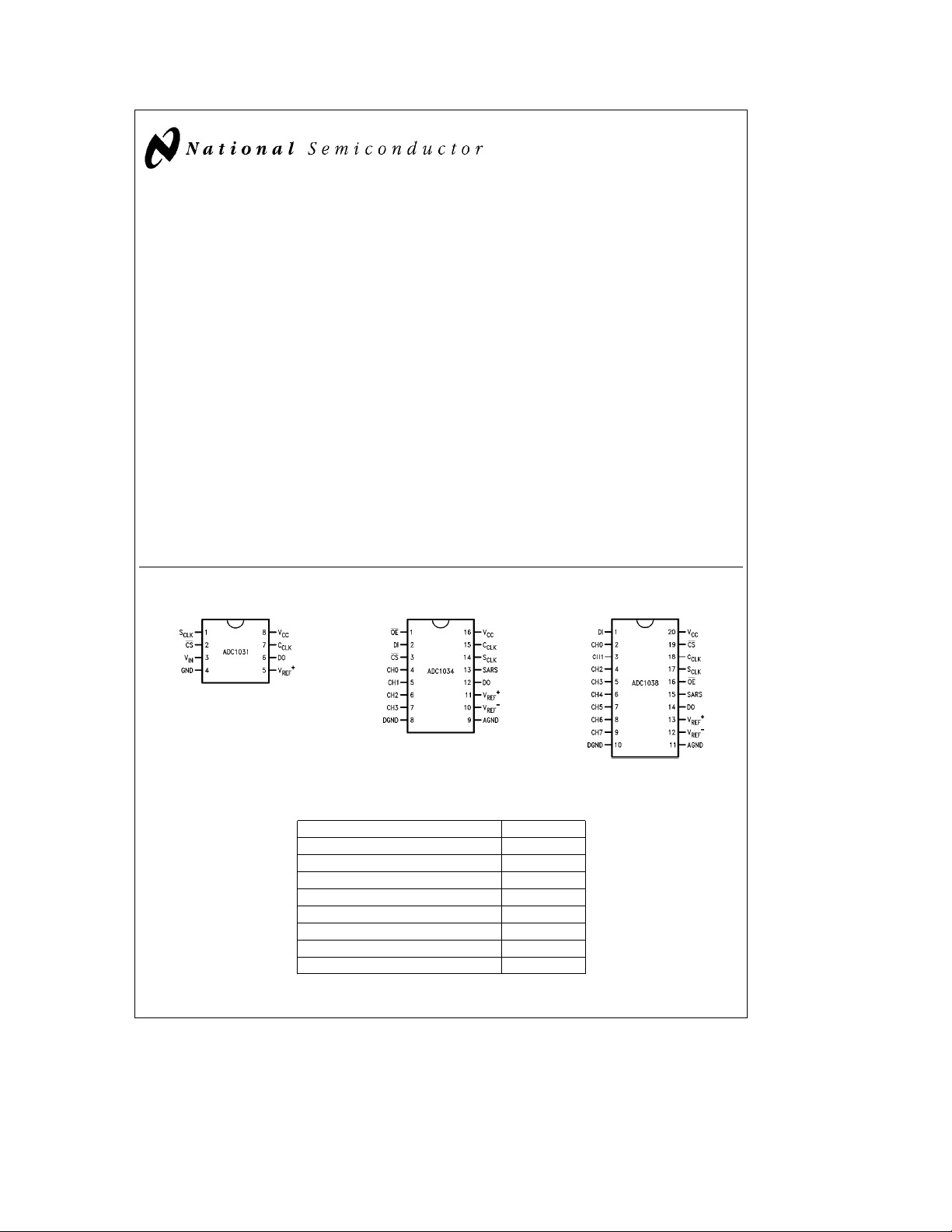
Connection Diagrams
Dual-In-Line and SO Packages
Top View
ADC1031 In NS Package N08E
Ordering Information
C
1995 National Semiconductor Corporation RRD-B30M75/Printed in U. S. A.
TL/H/10556– 4
Top View
ADC1034 In NS Packages
J16A, M16B or N16E
s
Industrialb40§CsT
a
85§C Package
A
ADC1031CIN N08E
ADC1034CIN N16E
ADC1034CIWM M16B
ADC1038CIN N20A
ADC1038CIWM M20B
s
Militaryb55§CsT
a
125§C Package
A
ADC1034CMJ J16A
ADC1038CMJ J20A
TL/H/10556
TL/H/10556– 3
TL/H/10556– 2
Top View
ADC1038 In NS Packages
J20A, M20B or N20A
Page 2
Absolute Maximum Ratings (Notes1&3)
If Military/Aerospace specified devices are required,
please contact the National Semiconductor Sales
Office/Distributors for availability and specifications.
Supply Voltage (V
Voltage at Inputs and Outputs
Input Current at Any Pin (Note 4)
Package Input Current (Note 4)
Package Dissipation
e
at T
A
ESD Susceptability (Note 6) 2000V
Soldering Information
N Package (10 sec.) 260
J Package (10 sec.) 300
SO Package (Note 7):
Vapor Phase (60 sec.) 215
Infrared (15 sec.) 220
Storage Temperature
) 6.5V
CC
b
0.3V to V
CC
a
g
g
20 mA
0.3V
5mA
25§C (Note 5) 500 mW
b
65§Ctoa150§C
§
§
§
§
Operating Ratings (Notes2&3)
Temperature Range T
ADC1031CIN,
ADC1034CIN,
ADC1034CIWM,
ADC1038CIN,
ADC1038CIWM
ADC1034CMJ, ADC1038CMJ
Supply Voltage (VCC) 4.75 VDCto 5.25 V
Reference Voltage
(V
REF
a
e
b
V
REF
V
REF
C
C
C
C
b
b
) 2.0 VDCto V
MIN
b
40§CsT
55§CsT
s
s
T
T
A
MAX
s
a
85§C
A
s
a
125§C
A
DC
a
0.05V
CC
Electrical Characteristics
The following specifications apply for V
specified. Boldface limits apply for T
ea
5.0V, V
CC
e
e
T
A
T
J
MIN
REF
to T
MAX
ea
4.6V, f
; all other limits T
Symbol Parameter Conditions
CONVERTER AND MULTIPLEXER CHARACTERISTICS
Total Unadjusted CIN, CIWM, CMJ (Note 10)
Error
Differential Linearity 10 Bits (min)
R
REF
V
REF
V
IN
Reference Input Resistance 8 kX
Reference Voltage (V
Analog Input Voltage (Note 11) (V
On Channel Leakage Current On Channele5VDC, 5.0 200 nA (max)
Off Channel
e
0V
DC
(Note 12) On Channele0VDC, 5.0
Off Channele5V
DC
Off Channel Leakage Current On Channele5VDC, 5.0
Off Channel
e
0V
DC
(Note 12) On Channele0VDC, 5.0 200 nA (max)
DC
e
5V
DC
s
s
V
CC
Off Channel
Power Supply Zero Error 4.75 V
Sensitivity
Full Scale Error
S
5.25 V
e
700 kHz, and f
e
A
T
J
e
3 MHz unless otherwise
C
e
25§C.
Typical Limit Units
(Note 8) (Note 9) (Limits)
g
11 kX (max)
a
CC
a
CC
b
(GND
500 nA (max)
b
b
500 nA (max)
b
b
500 nA (max)
500 nA (max)
g
DC
1/4 LSB (max)
g
1/4 LSB (max)
1 LSB (max)
5 kX (min)
0.05) V (max)
0.05) V (max)
0.05) V (min)
200 nA (max)
200 nA (max)
2
Page 3
Electrical Characteristics (Continued)
The following specifications apply for V
specified. Boldface limits apply for T
ea
5.0V, V
CC
e
e
T
A
T
J
MIN
REF
to T
MAX
ea
4.6V, f
; all other limits T
S
Symbol Parameter Conditions
DIGITAL AND DC CHARACTERISTICS
V
IN(1)
V
IN(0)
I
IN(1)
I
IN(0)
V
OUT(1)
V
OUT(0)
I
OUT
I
SOURCE
I
SINK
I
CC
Logical ‘‘1’’ Input Voltage V
Logical ‘‘0’’ Input Voltage V
Logical ‘‘1’’ Input Current V
Logical ‘‘0’’ Input Current V
Logical ‘‘1’’ Output Voltage V
Logical ‘‘0’’ Output Voltage V
TRI-STATE Output Current V
Output Source Current V
Output Sink Current V
Supply Current CSeHIGH, V
e
5.25 V
I
OUT
V
CC
CC
IN
IN
CC
I
OUT
I
OUT
CC
OUT
OUT
OUT
OUT
e
e
DC
e
4.75 V
DC
5.0 V
DC
0V
DC
e
4.75 V
DC
eb
360 mA 2.4 V (min)
eb
10 mA 4.5 V (min)
e
4.75 V
DC
e
1.6 mA
e
0V
e
5V 0.01 3 mA (max)
e
0V
e
V
CC
Open 1.5 3 mA (max)
REF
AC CHARACTERISTICS
f
f
T
t
t
t
t1H,t0HDelay from OE or CS Rising R
t
t
Conversion Clock (C
C
Frequency 4.0 3.0 MHz (max)
Serial Data Clock (S
S
Frequency (Note 13) f
Conversion Time Not Including MUX Addressing and 41 (1/fC)
C
Analog Sampling Time After Address is Latched,CSeLow 4.5 (1/fS)
CA
Access Time Delay from CS or OE OEe‘‘0’’
ACC
Falling Edge to DO Data Valid
Set-up Time of CS Falling
SET-UP
Edge to S
Rising Edge
CLK
Edge to DO TRI-STATE
DI Hold Time from S
HDI
DI Set-up Time to S
SDI
) 0.7 MHz (min)
CLK
)f
CLK
e
3 MHz, R/Le‘‘0’’ 183 kHz (min)
C
e
3 MHz, R/Le‘‘1’’ 622 kHz (min)
C
e
f
3 MHz, R/Le‘‘0’’ or R/Le‘‘1’’ 2 1.0 MHz (max)
C
Analog Input Sampling Times
e
L
Rising Edge 0 50 ns (min)
CLK
Rising Edge 50 100 ns (min)
CLK
3kX,C
e
100 pF
L
e
700 kHz, and f
e
A
e
3 MHz unless otherwise
C
e
T
25§C.
J
Typical Limit Units
(Note 8) (Note 9) (Limits)
2.0 V (min)
0.8 V (max)
0.005 2.5 mA (max)
b
0.005b2.5 mA (max)
0.4 V (max)
b
0.01
b
14
b
b
16 8.0 mA (min)
a
200 ns
a
200 ns
100 200 ns (max)
75 150 ns (min)
100 120 ns (max)
3 mA (max)
6.5 mA (min)
(max)
(max)
3
Page 4
Electrical Characteristics (Continued)
The following specifications apply for V
specified. Boldface limits apply for T
Symbol Parameter Conditions
ea
5.0V, V
CC
e
e
T
A
T
J
MIN
REF
to T
MAX
ea
4.6V, f
; all other limits T
S
e
700 kHz, and f
e
A
e
3 MHz unless otherwise
C
e
T
25§C.
J
Typical Limit Units
(Note 8) (Note 9) (Limits)
AC CHARACTERISTICS (Continued)
t
HDO
t
DDO
t
RDO
t
FDO
C
DO Hold Time from S
Delay from S
Edge to DO Data Valid
CLK
Falling Edge R
CLK
Falling R
DO Rise Time R
DO Fall Time R
IN
Input Capacitance Analog Inputs (CH0 – CH7) 50 pF
e
30 kX,C
L
e
30 kX,C
L
e
30 kX, TRI-STATE to High 35 75 ns (max)
L
e
C
100 pF
L
e
30 kX, TRI-STATE to Low 35 75 ns (max)
L
e
C
100 pF
L
e
100 pF 70 10 ns (min)
L
e
100 pF
L
150 250 ns (max)
Low to High 75 150 ns (max)
High to Low 75 150 ns (max)
All Other Inputs 7.5 pF
Note 1: Absolute Maximum Ratings indicate limits beyond which damage to the device may occur.
Note 2: Operating Ratings indicate conditions for which the device is functional, but do not guarantee specific performance limits. For guaranteed specifications
and test conditions, see the Electrical Characteristics. The guaranteed specifications apply only for the test conditions listed. Some performance characteristics
may degrade when the device is not operated under the listed test conditions.
Note 3: All voltages are measured with respect to AGND and DGND, unless otherwise specified.
Note 4: When the input voltage (V
20 mA maximum package input current rating limits the number of pins that can safely exceed the power supplies with an input current of 5 mA to four pins.
Note 5: The maximum power dissipation must be derated at elevated temperatures and is dictated by T
allowable power dissipation at any temperature is P
device, T
suffixes 52
46
Note 6: Human body model, 100 pF capacitor discharged through a 1.5 kX resistor.
Note 7: See AN450 ‘‘Surface Mounting Methods and Their Effect on Product Reliability’’ or
soldering surface mount devices.
Note 8: Typicals are at T
Note 9: Limits are guaranteed to National’s AOQL (Average Outgoing Quality Level).
Note 10: Total unadjusted error includes offset, full-scale, linearity, multiplexer, and hold step errors.
Note 11: Two on-chip diodes are tied to each analog input. They will forward-conduct for analog input voltages one diode drop below ground or one diode drop
greater than V
elevated temperatures, which will cause errors for analog inputs near full-scale. The spec allows 50 mV forward bias of either diode; this means that as long as the
analog V
reading of a selected channel. To achieve an absolute 0 V
temperature variations, initial tolerance and loading.
Note 12: Channel leakage current is measured after the channel selection.
Note 13: In order to synchronize the serial data exchange properly, SARS needs to go low after completion of the serial I/O data exchange. If this does not occur
the output shift register will be reset and the correct output data lost. The minimum limit for S
justified, and can be determined by the following equations:
e
125§C. The typical thermal resistance (iJA) of these parts when board mounted follow: ADC1031 with CIN suffixes 71§C/W, ADC1034 with CMJ
Jmax
C/W, ADC1034 with CIN suffixes 54§C/W, ADC1034 with CIWM suffixes 70§C/W, ADC1038 with CMJ suffixes 53§C/W, ADC1038 with CIN suffixes
§
C/W, ADC1038 with CIWM suffixes 64§C/W.
§
supply. Be careful during testing at low VCClevels (4.5V), as high level analog inputs (5V) can cause an input diode to conduct, especially at
CC
does not exceed the supply voltage by more than 50 mV, the output code will be correct. Exceeding this range on an unselected channel will corrupt the
IN
) at any pin exceeds the power supplies (V
IN
e
b
(T
D
Jmax
e
25§C and represent most likely parametric norm.
J
to5VDCinput voltage range will therefore require a minimum supply voltage of 4.950 VDCover
DC
l
(8.5/41) (fC) with right-justification (R/Le‘‘1’’) and f
f
S
TA)/iJAor the number given in the Absolute Maximum Ratings, whichever is lower. For this
k
IN
DGND, or V
l
S
l
VCC) the current at that pin should be limited to 5 mA. The
IN
, iJAand the ambient temperature, TA. The maximum
Jmax
Linear Databook
will depend on C
CLK
(2.5/41) (fC) with left-justification (R/Le‘‘0’’).
section ‘‘Surface Mount’’ for other methods of
frequency and whether right-justified or left-
CLK
4
Page 5
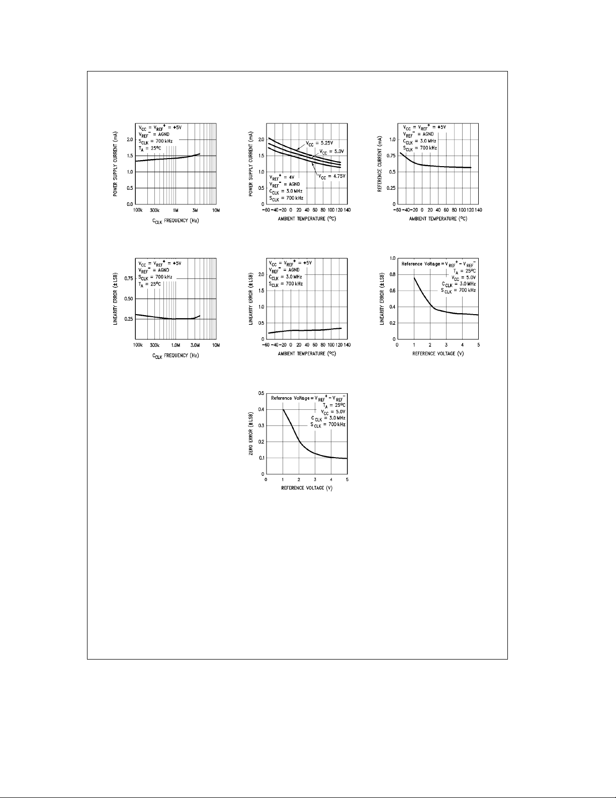
Typical Performance Characteristics
Power Supply Current
(ICC)vsC
CLK
Linearity Error vs
Frequency
C
CLK
Power Supply Current (ICC)
vs Ambient Temperature
Linearity Error vs
Ambient Temperature
Zero Error vs
Reference Voltage
Reference Current (I
vs Ambient Temperature
REF
Linearity Error vs
Reference Voltage
)
TL/H/10556– 5
5
Page 6
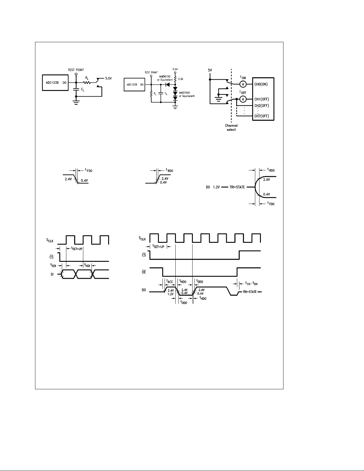
Test Circuits
t1H,t
0H
Timing Diagrams
DO High to Low State
DI Data Input Timing
TL/H/10556– 6
TL/H/10556– 9
DO except ‘‘TRI-STATE’’
TL/H/10556– 7
DO Low to High State
TL/H/10556– 10
DO Data Output Timing
Leakage Current
TL/H/10556– 8
DO ‘‘TRI-STATE’’ Rise
and Fall Times
TL/H/10556– 11
TL/H/10556– 12
TL/H/10556– 13
6
Page 7

Timing Diagrams (Continued)
ADC1031 CS
High during Conversion
ADC1038/ADC1034 CS High during Conversion
TL/H/10556– 14
C
continuously enabled
CLK
TL/H/10556– 15
7
Page 8

Timing Diagrams (Continued)
C
continuously enabled
CLK
ADC1038/ADC1034 CS
Low Continuously
Multiplexer Address/Channel Assignment Tables
ADC1038
MUX Address Analog
A2 A1 A0
Channel
Selected
0 0 0 CH0
0 0 1 CH1
0 1 0 CH2
0 1 1 CH3
1 0 0 CH4
1 0 1 CH5
1 1 0 CH6
1 1 1 CH7
Note: ‘‘X’’edon’t care
MUX Address Analog
A2 A1 A0
X 0 0 CH0
X 0 1 CH1
X 1 0 CH2
X 1 1 CH3
TL/H/10556– 16
ADC1034
Channel
Selected
8
Page 9

ADC1038 Functional Block Diagram
TL/H/10556– 17
9
Page 10

1.0 Pin Descriptions
C
S
DI The serial data input pin. The data applied to this
DO The data output pin. The A/D conversion result
SARS This pin is an output and indicates the status of
CS
OE The output enable pin. When OE and CS are
CH0– The analog inputs of the MUX. A channel input is
CH7 selected by the address information at the DI pin,
The clock applied to this input controls the suc-
CLK
cessive approximation conversion time interval.
The clock frequency applied to this input can be
between 700 kHz and 4 MHz.
The serial data clock input. The clock applied to
CLK
this input controls the rate at which the serial
data exchange occurs and the analog sampling
time available to acquire an analog input voltage.
The rising edge loads the information on the DI
pin into the multiplexer address shift register (address register). This address controls which
channel of the analog input multiplexer (MUX) is
selected.
The falling edge shifts the data resulting from the
previous A/D conversion out on DO. CS
enable or disable the above functions.
pin is shifted by S
dress register. The first 3 bits of data (A0–A2)
into the multiplexer ad-
CLK
are the MUX channel address (see the Multiplexer Address/Channel Assignment tables). The
fourth bit (R/L
) determines the data format of the
conversion result in the conversion to be started.
When R/L
is low the output data format is leftjustified; when high it is right-justified. When rightjustified, six leading ‘‘0’’s are output on DO before the MSB information; thus the complete conversion result is shifted out in 16 clock periods.
(D0–D9) is output on this pin. This result can be
left- or right-justified depending on the value of
R/L
bit shifted in on DI.
the internal successive approximation register
(SAR). When high, it signals that the A/D conversion is in progress. This pin is set high after the
analog input sampling time (t
high for 41 C
the output shift register has been loaded with the
periods. When SARS goes low,
CLK
conversion result and another A/D conversion
sequence can be started.
The chip select pin. When a low is applied to this
pin, the rising edge of S
into the address register. In the ADC1031 this pin
also functions as the OE
CLK
pin.
both low the falling edge of S
previous A/D conversion data on the DO pin.
which is loaded on the rising edge of S
the address register.
Source impedances (R
should be kept below 1 kX.IfR
) driving these inputs
S
1kX, the sampled data comparator will not have
enough time to acquire the correct value of the
applied input voltage.
The voltage applied to these inputs should not
exceed V
more than 50 mV. Exceeding this range on an
or go below DGND or AGND by
CC
unselected channel will corrupt the reading of a
selected channel.
and OE
) and remains
CA
shifts the data on DI
shifts out the
CLK
into
CLK
is greater than
S
a
V
V
The positive analog voltage reference for the an-
REF
alog inputs. In order to maintain accuracy the
voltage range of V
b
V
) is 2.5 VDCto 5.0 VDCand the voltage at
REF
a
V
cannot exceed V
REF
ADC1031 V
b
The negative voltage reference for the analog in-
REF
puts. In order to maintain accuracy the voltage at
b
is always GND.
REF
REF(VREF
CC
e
V
REF
a
50 mV. In the
a
this pin must not go below DGND and AGND by
more than 50 mV or exceed 40% of V
e
5V, V
V
V
CC
REF
The power supply pin. The operating voltage
range of V
should be bypassed with 10 mF and 0.1 mF ca-
b
(max)e2V). In the ADC1031
REF
b
is internally connected to the GND pin.
is 4.75 VDCto 5.25 VDC.V
CC
CC
(for V
pacitors to digital ground for proper operation of
the A/D converter.
DGND, The digital and analog ground pins for the
AGND ADC1034 and the ADC1038. In order to maintain
accuracy the voltage difference between these
two pins must not exceed 300 mV.
GND The digital and analog ground pin for the
ADC1031.
2.0 Functional Description
2.1 DIGITAL INTERFACE
The ADC1034 and ADC1038 implement their serial interface via seven digital control lines. There are two clock inputs for the ADC1034/ADC1038. The S
rate at which the serial data exchange occurs and the duration of the analog sampling time window. The C
the conversion time and must be continuously enabled. A
low on CS
enables the rising edge of S
serial multiplexer addressing data on the DI pin. The first
three bits of this data select the analog input channel for the
ADC1038 and the ADC1034 (see the Channel Addressing
Tables). The following bit, R/L
, selects the output data format (right-justified or left-justified) for the conversion to be
started. With CS
TRI-STATE) and the falling edge of S
from the previous analog conversion. When the first conver-
and OE low the DO pin is active (out of
CLK
sion is started the data shifted out on DO is erroneous as it
depends on the state of the Parallel Load 16-Bit Shift Register on power up, which is unpredictable.
The ADC1031 implements its serial interface with only four
control pins since it has only one analog input and comes in
an eight pin mini-dip package. The S
pins are available for the serial interface. The output data
CLK,CCLK
format cannot be selected and defaults to a left-justified
format. The state of DO is controlled by CS
2.2 OUTPUT DATA FORMAT
When R/L
is low the output data format is left-justified;
when high it is right-justified. When right-justified, six leading
‘‘0’’s are output on DO before the MSB, and the complete
conversion result is shifted out in 16 clock periods.
2.3.0 CS
HIGH DURING CONVERSION
With a continuous S
nize the serial data exchange. A valid CS
occurs at least 100 ns (t
S
, thus causing data to be input on DI. If this does not
CLK
input, CS must be used to synchro-
CLK
) before the rising edge of
SET-UP
controls the
CLK
controls
CLK
to shift in the
CLK
shifts out the data
,CSand DO
only.
is recognized if it
b
CC
CC
10
Page 11

2.0 Functional Description (Continued)
occur there will be an uncertainty as to which S
edge will clock in the first bit of data. CS
must remain low
during the complete I/O exchange. Also, OE
low if data from the previous conversion needs to be accessed.
2.3.1 CS
LOW CONTINUOUSLY
Another way to accomplish synchronous serial communication is to tie CS
synchronize the serial data exchange. S
low during the conversion time and enabled after SARS
goes low. With CS
low continuously and use SARS and S
can be disabled
CLK
low during the conversion time a zero will
remain on DO until the conversion is completed. Once the
conversion is complete, the falling edge of SARS will shift
out on DO the MSB before S
would be a leading zero if right-justified or D9 if left-justified.
is enabled. This MSB
CLK
The rest of the data will be shifted out once S
as discussed previously. If CS
goes high during the conversion sequence DO is put into TRI-STATE, and the conversion result is not affected so long as CS
remains high until
the end of the conversion.
2.4 TYING S
S
and C
CLK
time will increase because the maximum clock frequency is
and C
CLK
can be tied together. The total conversion
CLK
TOGETHER
CLK
now 1 MHz. The timing diagrams and the serial I/O exchange time (10 S
version time (T
mum of 14 ms to a minimum of 41 ms. In the case where CS
cycles) remain the same, but the con-
CLK
e
41 C
C
cycles) lengthens from a mini-
CLK
is low continuously, since the applied clock cannot be disabled, SARS must be used to synchronize the data output
on DO and initiate a new conversion. The falling edge of
SARS sends the MSB information out on DO. The next rising edge of the clock shifts in MUX address bit A2 on DI.
The following clock falling edge will clock the next data bit
of information out on DO. A conversion will be started after
MUX addressing information has been loaded in (3 more
clocks) and the analog sampling time (4.5 clocks) has
elapsed. The ADC1031 does not have SARS. Therefore, CS
cannot be left low continuously on the ADC1031.
CLK
needs to be
is enabled
CLK
rising
CLK
3.0 Analog Considerations
3.1 THE INPUT SAMPLE AND HOLD
The ADC1031/4/8’s sample/hold capacitor is implemented
in its capacitive ladder structure. After the channel address
is received, the ladder is switched to sample the proper analog input. This sampling mode is maintained for 4.5 S
cycles after the multiplexer addressing information is loaded
in. For the ADC1031/4/8, the sampling of the analog input
starts on S
’s 4th rising edge.
CLK
CLK
An acquisition window of 4.5 S
allow the ladder capacitance to settle to the analog input
cycles is available to
CLK
voltage. Any change in the analog voltage before or after
the acquisition window will not effect the A/D conversion
result.
In the most simple case, the ladder’s acquisition time is determined by the R
C
(3.5 pF) and the total ladder (CL) and stray (CS2) capac-
S1
itance (48 pF). For large source resistance the analog input
can be modeled as an RC network as shown in
to
The values shown yield an acquisition time of about 3 ms for
(9 kX) of the multiplexer switches, the
on
10 bit accuracy with a zero to a full scale change in the
reading. External source resistance and capacitance will
lengthen the acquisition time and should be accounted for.
The curve ‘‘Signal to Noise Ratio vs Output Frequency’’
(Figure 2)
gives an indication of the usable bandwidth of the
ADC1031/ADC1034/ADC1038. The signal to noise ratio of
an ideal A/D is the ratio of the RMS value of the full scale
input signal amplitude to the value of the total error amplitude (including noise) caused by the transfer function of the
A/D. An ideal 10 bit A/D converter with a total unadjusted
error of 0 LSB would have a signal to noise ratio of about
62 dB, which can be derived from the equation:
e
S/N
6.02(N)a1.8
where S/N is in dB and N is the number of bits.
shows the signal to noise ratio vs. input frequency of a typical ADC1031/4/8 with (/2 LSB total unadjusted error. The
dotted lines show signal-to-noise ratios for an ideal (noiseless) 10 bit A/D with 0 LSB error and an A/D witha1LSB
error.
The sample-and-hold error specifications are included in the
error and timing specifications of the A/D. The hold step
and gain error sample/hold specs are taken into account in
the ADC1031/4/8’s total unadjusted error specification,
while the hold settling time is included in the A/D’s maximum conversion time specification. The hold droop rate can
be thought of as being zero since an unlimited amount of
time can pass between a conversion and the reading of
data. However, once the data is read it is lost and another
conversion is started.
3.2 INPUT FILTERING
Due to the sampling nature of the analog input, transients
will appear on the input pins. They are caused by the ladder
capacitance and internal stray capacitance charging current
flowing into V
performance if they settle out within the sampling window.
. These transients will not degrade the A/D’s
IN
This will occur if external source resistance is kept to a minimum.
Figure 1
Figure 2
.
FIGURE 1. Analog Input Model
TL/H/10556– 18
TL/H/10556– 19
FIGURE 2. ADC1031/4/8 Signal to
Noise Ratio vs Input Frequency
11
Page 12

3.0 Analog Considerations (Continued)
External Reference 2.5V Full Scale
TL/H/10556– 20
Power Supply as Reference
FIGURE 3. Analog Input Options
3.3 REFERENCE AND INPUT
The two V
tial and define the zero to full-scale input range of the A to D
inputs of the ADC1031/4/8 are fully differen-
REF
converter. This allows the designer to easily vary the span
of the analog input since this range will be equivalent to the
voltage difference between V
ing V
REF(VREF
sensitivity of the converter can be increased (i.e., if V
e
V
REF
2V then 1 LSBe1.95 mV). The input/reference arrange-
ab
a
and V
REF
b
V
) to less than 5V, the
REF
REF
b
. By reduc-
REF
Power Supply Bypassing
Input Not Referred to GND
TL/H/10556– 21
TL/H/10556– 22
b
(
*Current path must still exist from V
ground
)
to
IN
ment also facilitates ratiometric operation and in many
cases the chip power supply can be used for transducer
power as well as the V
This reference flexibility lets the input span not only be varied but also offset from zero. The voltage at V
input level which produces a digital output of all zeros.
e
Though V
allows nearly differential-input capability for many measure-
is not itself differential, the reference design
IN
ment applications.
source.
REF
Figure 3
shows some of the configura-
REF
b
sets the
tions that are possible.
The ADC1031 has no V
GND.
REF
b
pin. V
b
is internally tied to
REF
TL/H/10556– 23 TL/H/10556– 24
12
Page 13

Protecting the Analog Inputs
Diodes are IN914
TL/H/10556– 25
Zero-Shift and Span-Adjust (2VsV
*1% resistors
TL/H/10556– 26
s
4.5V)
IN
TL/H/10556– 27
13
Page 14

14
Page 15

Physical Dimensions inches (millimeters)
Order Number ADC1034CMJ
NS Package Number J16A
Order Number ADC1038CMJ
NS Package Number J20A
15
Page 16

Physical Dimensions inches (millimeters) (Continued)
Order Number ADC1034CIWM
NS Package Number M16B
Order Number ADC1038CIWM
NS Package Number M20B
16
Page 17
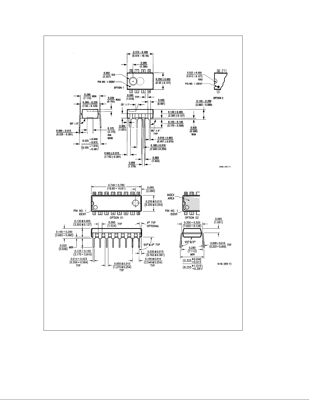
Physical Dimensions inches (millimeters) (Continued)
Order Number ADC1031CIN
NS Package Number N08E
Order Number ADC1034CIN
NS Package Number N16E
17
Page 18

Physical Dimensions inches (millimeters) (Continued) Lit.
Order Number ADC1038CIN
NS Package Number N20A
with Analog Multiplexer and Track/Hold Function
Ý
101002
ADC1031/ADC1034/ADC1038 10-Bit Serial I/O A/D Converters
LIFE SUPPORT POLICY
NATIONAL’S PRODUCTS ARE NOT AUTHORIZED FOR USE AS CRITICAL COMPONENTS IN LIFE SUPPORT
DEVICES OR SYSTEMS WITHOUT THE EXPRESS WRITTEN APPROVAL OF THE PRESIDENT OF NATIONAL
SEMICONDUCTOR CORPORATION. As used herein:
1. Life support devices or systems are devices or 2. A critical component is any component of a life
systems which, (a) are intended for surgical implant support device or system whose failure to perform can
into the body, or (b) support or sustain life, and whose be reasonably expected to cause the failure of the life
failure to perform, when properly used in accordance support device or system, or to affect its safety or
with instructions for use provided in the labeling, can effectiveness.
be reasonably expected to result in a significant injury
to the user.
National Semiconductor National Semiconductor National Semiconductor National Semiconductor National Semiconductores National Semiconductor
Corporation GmbH Japan Ltd. Hong Kong Ltd. Do Brazil Ltda. (Australia) Pty, Ltd.
2900 Semiconductor Drive Livry-Gargan-Str. 10 Sumitomo Chemical 13th Floor, Straight Block, Rue Deputado Lacorda Franco Building 16
P.O. Box 58090 D-82256 F4urstenfeldbruck Engineering Center Ocean Centre, 5 Canton Rd. 120-3A Business Park Drive
Santa Clara, CA 95052-8090 Germany Bldg. 7F Tsimshatsui, Kowloon Sao Paulo-SP Monash Business Park
Tel: 1(800) 272-9959 Tel: (81-41) 35-0 1-7-1, Nakase, Mihama-Ku Hong Kong Brazil 05418-000 Nottinghill, Melbourne
TWX: (910) 339-9240 Telex: 527649 Chiba-City, Tel: (852) 2737-1600 Tel: (55-11) 212-5066 Victoria 3168 Australia
National does not assume any responsibility for use of any circuitry described, no circuit patent licenses are implied and National reserves the right at any time without notice to change said circuitry and specifications.
Fax: (81-41) 35-1 Ciba Prefecture 261 Fax: (852) 2736-9960 Telex: 391-1131931 NSBR BR Tel: (3) 558-9999
Tel: (043) 299-2300 Fax: (55-11) 212-1181 Fax: (3) 558-9998
Fax: (043) 299-2500
 Loading...