

Page 1

ADC10321
10-Bit, 20MSPS, 98mW A/D Converter with Internal
Sample and Hold
General Description
The ADC10321 is a low power, high performance CMOS
analog-to-digital converter that digitizes signals to 10 bits
resolution at sampling rates up to 25Msps while consuming
a typical 98mW from a single 5V supply. Reference force
and sense pins allow the user to connect an external reference buffer amplifier to ensure optimal accuracy. No missing
codes is guaranteed over the full operating temperature
range. The unique two stage architecture achieves 9.2 Effective Bits with a 10MHz input signal and a 20MHz clock
frequency. Output formatting is straight binary coding.
To ease interfacing to 3V systems, the digital I/O power pins
of the ADC10321 can be tied to a 3V power source, making
the outputs 3V compatible. When not converting, power
consumption can be reduced by pulling the PD (Power
Down) pin high, placing the converter into a low power
standby state, where it typically consumes less than 4mW.
The ADC10321’s speed, resolution and single supply operation makes it well suited for a variety of applications in video,
imaging, communications, multimedia and high speed data
acquisition. Low power, single supply operation ideally suit
the ADC10321 for high speed portable applications, and its
speed and resolution are ideal for charge coupled device
(CCD) input systems.
The ADC10321 comes in a space saving 32-pin TQFP and
operates over the industrial (−40˚C ≤ T
ture range.
≤ +85˚C) tempera-
A
n Guaranteed No Missing Codes
n Tri-State Outputs
n TTL/CMOS or 3V Logic Input/Output Compatible
Key Specifications
n Resolution 10 Bits
n Conversion Rate 20 Msps
n ENOB
n DNL 0.35 LSB (typ)
n Conversion Latency 2 Clock Cycles
n PSRR 56dB
n Power Consumption 98mW (typ)
n Low Power Standby Mode
@
10MHz Input 9.2 Bits (typ)
Applications
n Digital Video
n Communications
n Document Scanners
n Medical Imaging
n Electro-Optics
n Plain Paper Copiers
n CCD Imaging
January 2003
<
4mW (typ)
ADC10321 10-Bit, 20MSPS, 98mW A/D Converter with Internal Sample and Hold
Features
n Internal Sample-and-Hold
n Single +5V Operation
n Low Power Standby Mode
© 2003 National Semiconductor Corporation DS100897 www.national.com
Page 2
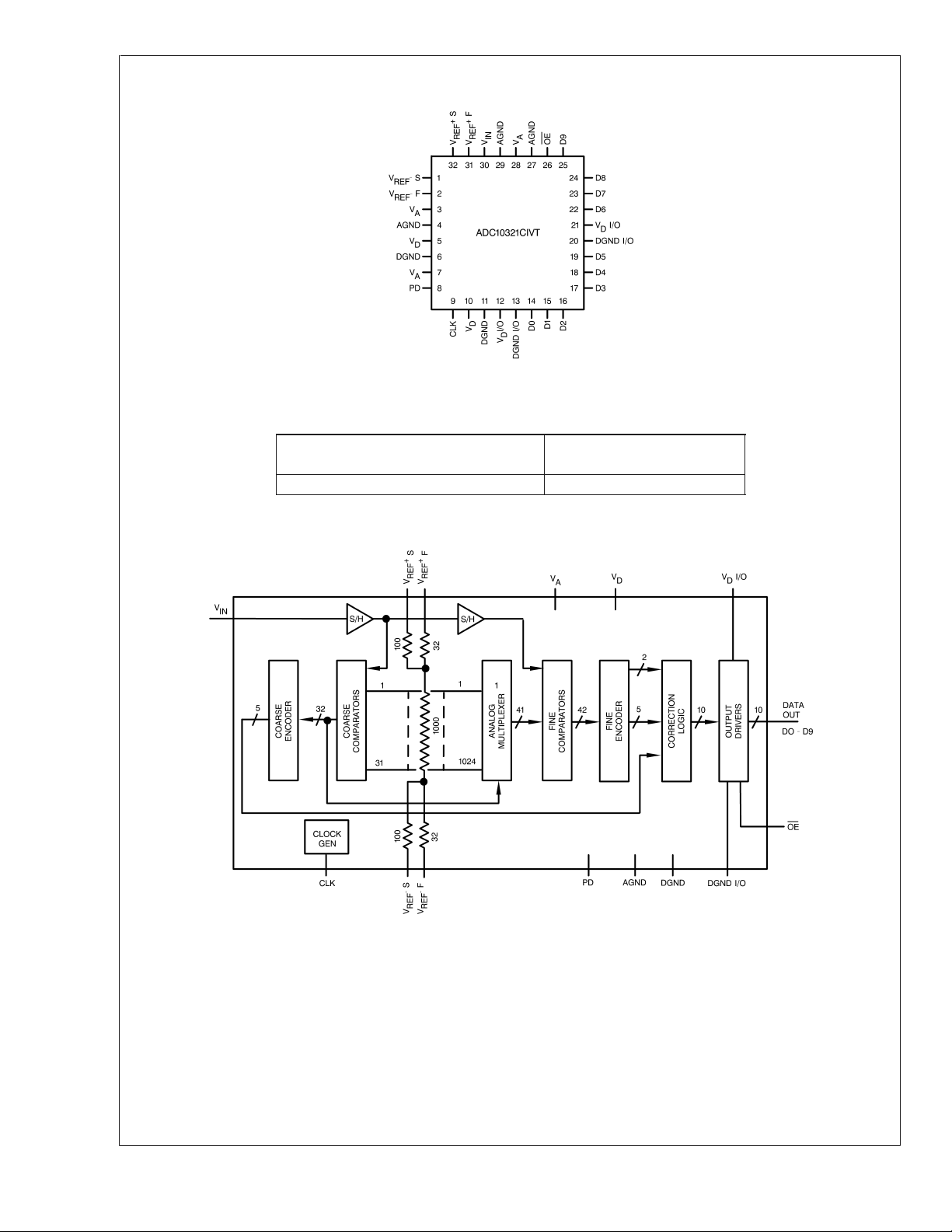
Connection Diagram
ADC10321
Ordering Information
Block Diagram
10089701
Commercial
(−40˚C ≤ T
ADC10321CIVT TQFP
≤ +85˚C) NS Package
A
www.national.com 2
10089702
Page 3
Pin Descriptions and Equivalent Circuits
ADC10321
Pin
No. Symbol Equivalent Circuit
Analog I/O
30 V
31 V
32 V
2V
1V
IN
REF
REF
REF
REF−
+
F
+
S
−
F
S
9 CLK
Description
Analog Input signal to be converted. Conversion
range is V
REF
+
StoV
REF
−
S.
Analog input that goes to the high side of the
reference ladder of the ADC. This voltage should
+
force V
S to be in the range of 2.3V to 4.0V.
REF
Analog output used to sense the voltage near the top
of the ADC reference ladder.
Analog input that goes to the low side of the
reference ladder of the ADC. This voltage should
force V
S to be in the range of 1.3V to 3.0V.
REF−
Analog output used to sense the voltage near the
bottom of the ADC reference ladder.
Converter digital clock input. VINis sampled on the
falling edge of CLK input.
8PD
26 OE
14 thru
19
and
D0 -D9
22 thru
25
3, 7, 28 V
A
Power Down input. When this pin is high, the
converter is in the Power Down mode and the data
output pins are in a high impedance state.
Output Enable pin. When this pin and the PD pin are
low, the output data pins are active. When this pin or
the PD pin is high, the output data pins are in a high
impedance state.
Digital Output pins providing the 10 bit conversion
results. D0 is the LSB, D9 is the MSB. Valid data is
present just after the falling edge of the CLK input.
Positive analog supply pins. These pins should be
connected to a clean, quiet voltage source of +5V. V
and VDshould have a common supply and be
separately bypassed with 10µF to 50µF capacitors in
parallel with 0.1µF capacitors.
A
www.national.com3
Page 4
Pin Descriptions and Equivalent Circuits (Continued)
Pin
ADC10321
No. Symbol Equivalent Circuit
Description
Positive digital supply pins. These pins should be
connected to a clean, quiet voltage source of +5V. V
5, 10 V
D
and VDshould have a common supply and be
separately bypassed with 10µF to 50µF capacitors in
parallel with 0.1µF capacitors.
Positive supply pins for the digital output drivers.
12, 21 V
I/O
D
These pins should be connected to a clean, quiet
voltage source of +3V to +5V and be separately
bypassed with 10µF capacitors.
4, 27,
29
AGND
The ground return for the analog supply. AGND and
DGND should be connected together close to the
ADC10321 package.
The ground return for the digital supply. AGND and
6, 11 DGND
DGND should be connected together close to the
ADC10321 pacjage.
13, 20 DGND I/O The ground return of the digital output drivers.
A
www.national.com 4
Page 5
ADC10321
Absolute Maximum Ratings (Notes 1,
2)
If Military/Aerospace specified devices are required,
Machine Model 200V
Soldering Temp., Infrared, 10 sec. (Note 6) 235˚C
Storage Temperature −65˚C to +150˚C
please contact the National Semiconductor Sales Office/
Distributors for availability and specifications.
Positive Supply Voltage (V = V
Voltage on Any I/O Pin −0.3V to (V
) 6.5V
A=VD
or VD) +0.3V)
A
Input Current at Any Pin (Note 3)
Package Input Current (Note 3)
Package Dissipation at T
=
A
See (Note 4)
25˚C
ESD Susceptibility (Note 5)
Human Body Model 1500V
±
25mA
±
50mA
Operating Ratings(Notes 1, 2)
Operating Temperature −40˚C ≤ T
V
Supply Voltage +4.5V to +5.5V
A,VD
V
I/O Supply Voltage +2.7V to 5.5V
D
V
Voltage Range 1.3V to (VA-1.0V)
IN
V
+ Voltage Range 2.3V to (VA-1.0V)
REF
V
− Voltage Range 1.3V to 3.0V
REF
PD, CLK, OE Voltage
−0.3V to + 5.5V
≤ +85˚C
A
Converter Electrical Characteristics
The following specifications apply for VA= +5.0VDC,VD= 5.0VDC,VDI/O = 5.0VDC,V
= 20pF, f
C
L
= 20MHz, RS=25Ω. Boldface limits apply for TA=T
CLK
MIN
to T
MAX
Symbol Parameter Conditions
Static Converter Characteristics
INL Integral Non-Linearity
DNL Differential-Non Linearity
Resolution with No Missing
Codes
Zero Scale Offset Error −6 mV(max)
Full-Scale Error −6 mV(max)
Dynamic Converter Characteristics
f
= 1.0MHz
IN
ENOB Effective Number of Bits
S/(N+D)
Signal-to-Noise Plus
Distortion Ratio
SNR Signal-to-Noise Ratio
THD Total Harmonic Distortion
SFDR
Spurious Free Dynamic
Range
DG Differential Gain Error f
DP Differential Phase Error f
Overrange Output Code V
Underrange Output Code V
= 4.43MHz
f
IN
= 10MHz
f
IN
= 1.0MHz
f
IN
= 4.43MHz
f
IN
= 10MHz
f
IN
= 1.0MHz
f
IN
= 4.43MHz
f
IN
= 10MHz
f
IN
= 1.0MHz
f
IN
= 4.43MHz
f
IN
= 10MHz
f
IN
= 1.0MHz
f
IN
= 4.43MHz
f
IN
= 10MHz
f
IN
= 4.43MHz, f
IN
= 4.43MHz, f
IN
>
V
IN
<
V
IN
= 17.72MHz 0.5 %(max)
CLK
= 17.72MHz 0.5 deg(max)
CLK
+ 1023
REF
− 0
REF
BW Full Power Bandwidth 150 MHz
PSRR
Power Supply Rejection
Ratio
Change in Full Scale with 4.5V to 5.5V
Supply Change
Reference and Analog Input Characteristics
V
IN
Analog Input Range
+ = +3.5VDC,V
REF
− = +1.5VDC,
REF
: all other limits TA= 25˚C(Note 7)
Typical
(Note 8)
±
0.45
±
0.35
Limits
(Note 9)
±
1.0 LSB(max)
±
0.85 LSB(max)
10 Bits
9.5
9.5
9.0
Bits(min)
9.2
59
59
56
dB(min)
57
60
60
58
dB(min)
58
−71
−70
−59
dB(min)
−66
74
72
60
68
56 dB
1.3
4.0
Units
Bits
Bits
dB
dB
dB
dB
dB
dB
dB
dB
dB
V(min)
V(max)
www.national.com5
Page 6
Converter Electrical Characteristics (Continued)
The following specifications apply for VA= +5.0VDC,VD= 5.0VDC,VDI/O = 5.0VDC,V
= 20pF, f
C
L
ADC10321
= 20MHz, RS=25Ω. Boldface limits apply for TA=T
CLK
MIN
Symbol Parameter Conditions
C
IN
I
IN
R
REF
+ Positive Reference Voltage 3.5 4.0 V(max)
V
REF
V
− Negative Reference Voltage 1.5 1.3 V(min)
REF
(V
REF
(V
REF
Analog VINInput
Capacitance
Input Leakage Current 10 µA
Reference Ladder
Resistance
+) −
Total Reference Voltage 2.0
−)
DC and Logic Electrical Characteristics
The following specifications apply for VA= +5.0VDC,VD= +5.0VDC,VDI/O = 5.0VDC,V
= 20 pF, f
Symbol Parameter Conditions
CLK, OE, PD, Digital Input Characteristics
V
IH
V
IL
I
IH
I
IL
D00 - D13 Digital Output Characteristics
V
OH
V
OL
I
OZ
I
OS
Power Supply Characteristics
I
A
I/O Digital Supply Current
I
D+ID
P
D
= 20MHz, RS=25Ω. Boldface limits apply for TA=T
CLK
MIN
to T
Logical "1" Input Voltage VD= 5.5V 2.0 V(min)
Logical "0" Input Voltage VD= 4.5V 1.0 V(max)
Logical "1" Input Current VIH=V
D
Logical "0" Input Current VIL= DGND −10 µA
Logical "1" Output
Voltage
Logical "0" Output
Voltage
TRI-STATE Output
Current
Output Short Circuit
Current
Analog Supply Current
VDI/O = + 4.5V, I
I/O = + 2.7V, I
V
D
VDI/O = + 4.5V, I
I/O = + 2.7V, I
V
D
V
= DGND
OUT
V
OUT=VD
OUT
OUT
OUT
OUT
= −0.5mA
= −0.5mA
= −1.6mA
= −1.6mA
VDI/O=3V
V
I/O=5V
D
PD = LOW, Ref not included
PD = HIGH, Ref not included
PD = LOW, Ref not included
PD = HIGH, Ref not included
Power Consumption 98 110 mW (max)
+ = +3.5VDC,V
to T
REF
: all other limits TA= 25˚C(Note 7)
MAX
Typical
(Note 8)
Limits
(Note 9)
5pF
1000
+ = +3.5VDC,V
REF
: all other limits TA= 25˚C(Note 7)
MAX
Typical
(Note 8)
Limits
(Note 9)
10 µA
4.0
2.4
0.4
0.4
−10
10
±
12 mA
±
25 mA
14.5
0.5
5
0.2
16 mA(max)
6 mA(max)
− = +1.5VDC,
REF
850
1150
1.0
2.7
− = +1.5VDC,C
REF
Units
Ω(min)
Ω(max)
V(min)
V(max)
L
Units
V(min)
V(min)
V(max)
V(max)
µA
µA
AC Electrical Characteristics
The following specifications apply for VA= +5.0VDC,VDI/O = 5.0VDC,V
=tfc= 5ns, RS=25Ω.CL(data bus loading) = 20 pF, Boldface limits apply for TA=T
25˚C(Note 7)
Symbol Parameter Conditions
f
CLK1
f
CLK2
t
CH
t
CL
Maximum Clock Frequency 25 20 MHz(min)
Minimum Clock Frequency 1 MHz(max)
Clock High Time 23 ns(min
Clock Low Time 23 ns(min)
Duty Cycle 50
www.national.com 6
+ = +3.5VDC,V
REF
Typical
(Note 8)
− = +1.5VDC,f
REF
to T
MIN
: all other limits TA=
MAX
CLK
Limits
(Note 9)
45
55
= 20MHz, t
Units
(Limits)
%(min)
%(max)
rc
Page 7

AC Electrical Characteristics (Continued)
The following specifications apply for VA= +5.0VDC,VDI/O = 5.0VDC,V
=tfc= 5ns, RS=25Ω.CL(data bus loading) = 20 pF, Boldface limits apply for TA=T
25˚C(Note 7)
Symbol Parameter Conditions
Pipeliine Delay (Latency) 2.0 Clock Cycles
t
rc,tfc
t
r,tf
t
OD
t
OH
Clock Input Rise and Fall Time 5 ns(max)
Output Rise and Fall Times 10 ns
Fall of CLK to data valid 20 25 ns(max)
Output Data Hold Time 12 ns
From output High, 2K
t
DIS
t
EN
t
VALID
t
AD
t
AJ
Rising edge of OE to valid data
Falling edge of OE to valid data 1K to V
Data valid time 40 ns
Apeture Delay 4 ns
Aperture Jitter
Full Scale Step Response t
Overrange Recovery Time
t
WU
Note 1: Absolute Maximum Ratings indicate limits beyond which damage to the device may occur. Operating Ratings indicate conditions for which the device is
functional, but do not guarantee specific performance limits. For guaranteed specifications and test conditions, see the Electrical Characteristics. The guaranteed
specifications apply only for the test conditions listed. Some performance characteristics may degrade when the device is not operated under the listed test
conditions.
Note 2: All voltages are measured with respect to GND = AGND = DGND = 0V, unless otherwise specified.
Note 3: When the input voltage at any pin exceeds the power supplies ( V
50mA maximum package input current rating limits the number of pins that can safely exceed the power supplies with an input current of 25mA to two.
Note 4: The absolute maximum junction temperature (T
junction-to-ambient thermal resistance (θ
TQFP, θ
device under normal operation will typically be about 110mW (98mW quiescent power + 2mW reference ladder power +10mW due to 10 TTL load on each digital
output). The values for maximum power dissipation listed above will be reached only when the ADC10321 is operated in a severe fault condition (e.g. when input
or output pins are driven beyond the power supply voltages, or the power supply polarity is reversed). Obviously, such conditions should always be avoided.
Note 5: Human body model is 100 pF capacitor discharged through a 1.5kΩ resistor. Machine model is 220 pF discharged through ZERO Ω.
Note 6: The 235˚C reflow temperature refers to infared reflow. For Vapor Phase Reflow (VPR), the following conditions apply: Maintain the temperature at the top
of the package body above 183˚C for a minimum 60 seconds. The temperature measured on the package body must not exceed 220˚C. Only one excursion above
183˚C is allowed per reflow cycle.
Note 7: The inputs are protected as shown below. Input voltage magnitudes up to 500mV beyond the supply rails will not damage this device. However, errors in
the A/D conversion can occur if the input goes above V
is 69˚C/W, so PDMAX = 1,811 mW at 25˚C and 942mW at the maximum operating ambient temperature of 85˚C. Note that the power dissipation of this
JA
PD low to 1/2 LSB accurate
conversion (Wake-Up time)
), and the ambient temperature (TA), and can be calculated using the formula PDMAX=(TJmax - TA)/θJA. In the 32-pin
JA
A
max) for this device is 150˚C. The maximum allowable power dissipation is dictated by TJmax, the
J
or below AGND by more than 300 mV.
to Ground
From output Low, 2K
I/O
to V
D
CC
= 10ns 1 conversion
r
V
step from (V
IN
+100mV) to (V
<
AGND or V
IN
+ = +3.5VDC,V
REF
Typical
(Note 8)
− = +1.5VDC,f
REF
to T
MIN
: all other limits TA=
MAX
CLK
Limits
(Note 9)
25 ns
18 ns
25 ns
<
30 ps
+
REF
REF
−)
1 conversion
700 ns
>
VAor VD), the current at that pin should be limited to 25mA. The
IN
= 20MHz, t
Units
(Limits)
ADC10321
rc
www.national.com7
Page 8

AC Electrical Characteristics (Continued)
ADC10321
10089711
Note 8: Typical figures are at TA=TJ= 25˚C, and represent most likely parametric norms.
Note 9: Tested limits are guaranteed to Nationsl’s AOQL (Average Outgoing Quality Level).
Note 10: When the input signal is between V
the output code will be 000h, or all 0s.
+ and (VA+ 300mV), the output code will be 3FFh, or all 1s. When the input signal is between −300 mV and V
REF
10089712 10089724
REF
−,
Typical Performance Characteristics V
A=VD=VD
I/O = 5V, f
= 20MHz, unless otherwise
CLK
specified.
Typical INL INL vs f
10089725
CLK
10089726 10089727
INL vs Clock Duty Cycle Typical DNL DNL vs f
DNL vs V
A
10089738
DNL vs Clock Duty Cycle
10089739
INL vs V
A
CLK
SINAD & ENOB vs
Temperature and f
10089728
IN
10089729
www.national.com 8
10089740
10089730
Page 9

ADC10321
Typical Performance Characteristics V
specified. (Continued)
SINAD & ENOB vs
SINAD & ENOB vs V
A
10089731
Spectral Response at 20 MSPs
10089735
f
CLK
A=VD=VD
and f
IN
10089732
I/O = 5V, f
= 20MHz, unless otherwise
CLK
IA+IDvs. Temperature
10089737
www.national.com9
Page 10

Specification Definitions
APERTURE JITTER is the variation in aperture delay from
sample to sample. Aperture jitter shows up as input noise.
ADC10321
APERTURE DELAY See Sampling Delay.
DIFFERENTIAL GAIN ERROR is the percentage difference
between the output amplitudes of a given amplitude small
signal, high frequency sine wave input at two different dc
input levels.
DIFFERENTIAL PHASE ERROR is the difference in the
output phase of a small signal sine wave input at two different dc input levels.
DIFFERENTIAL NON-LINEARITY (DNL) is the measure of
the maximum deviation from the ideal step size of 1 LSB.
EFFECTIVE NUMBER OF BITS (ENOB, or EFFECTIVE
BITS) is another method of specifying Signal-to-Noise and
Distortion Ratio (S/N+D or SINAD). ENOB is defined as
(SINAD −1.76) / 6.02.
FULL POWER BANDWIDTH is a measure of the frequency
at which the reconstructed output fundamental drops 3 dB
below its 1MHz value for a full scale input. The test is
performed with f
. The input frequency at which the output is −3 dB
f
CLK
relative to the1MHz input signal is the full power bandwidth.
FULL SCALE (FS) INPUT RANGE of the ADC is the input
range of voltages over which the ADC will digitize that input.
For V
(V
+ = 3.50V and V
REF
−) = 2.00V.
REF
FULL SCALE OFFSET ERROR is a measure of how far the
last code transition is from the ideal 1
and is defined as V
the voltage at which the transitions from code 1022 to 1023
occurs.
FULL SCALE STEP RESPONSE is defined as the time
required after V
−, and settles sufficiently for the converter to recover
V
REF
and make a conversion with its rated accuracy.
INTEGRAL NON-LINEARITY (INL) is a measure of the
deviation of each individual code from a line drawn from
negative full scale (
through positive full scale (1
transition). The deviation of any given code from this straight
line is measured from the center of that code value.
equal to 100 kHz plus integral multiples of
IN
− = 1.50V, FS = (V
REF
1
⁄2LSB below V
−1.5 LSB − V
1023
goes from V
IN
1
⁄2LSB below the first code transition)
REF
1
⁄2LSB above the last code
REF
−toV
+ , where V
+, or V
REF
REF
REF
1023
+) −
REF
+to
OUTPUT DELAY is the time delay after the fall of the input
clock before the data update is present at the output pins.
OUTPUT HOLD TIME is the length of time that the output
data is valid after the fall of the input clock.
OVER RANGE RECOVERY TIME is the time required after
V
goes from AGND to V
IN
+orVINgoes from VAto V
REF
REF
−
for the converter to recover and make a conversion with its
rated accuracy.
PIPELINE DELAY (LATENCY) is the number of clock cycles
between initiation of conversion and when that data is presented to the output driver stage. Data for any given sample
is available by the Pipeline Delay plus the Output Delay after
that sample is taken. New data is available at every clock
cycle, but the data lags the conversion by the pipeline delay.
PSRR (POWER SUPPLY REJECTION RATIO) is the ratio
of the change in dc power supply voltage to the resulting
change in Full Scale Error, expressed in dB.
SAMPLING (APERTURE) DELAY or APERTURE TIME is
that time required after the fall of the clock input for the
sampling switch to open. The sample is effectively taken this
amount of time after the fall of the clock input.
SIGNAL TO NOISE RATIO (SNR) is the ratio, expressed in
dB, of the rms value of the input signal to the rms value of the
sum of all other spectral components below one-half the
sampling frequency, not including harmonics or dc.
SIGNAL TO NOISE PLUS DISTORTION (S/(N+D) or SINAD) is the ratio, expressed in dB, of the RMS value of the
input signal to the RMS value of all of the other spectral
components below half the clock frequency, including har-
+
is
monics but excluding dc.
SPURIOUS FREE DYNAMIC RANGE (SFDR) is the differ-
ence, expressed in dB or dBc, between the RMS values of
the input signal and the peak spurious signal, where a
spurious signal is any signal present in the output spectrum
that is not present at the input.
TOTAL HARMONIC DISTORTION (THD) is the ratio, expressed in dB, of the rms total of the first six harmonic
components, to the rms value of the input signal.
ZERO SCALE OFFSET ERROR is the difference between
the ideal input voltage (
1
⁄2LSB) and the actual input voltage
that just causes a transition from an output code of zero to
an output code of one.
www.national.com 10
Page 11

Timing Diagram
ADC10321
10089717
FIGURE 2. AC Test Circuit
FIGURE 1. ADC10321 Timing Diagram
FIGURE 3. tEN,t
Test Circuit
DIS
10089715
10089716
www.national.com11
Page 12

Functional Description
The ADC10321 maintains excellent dynamic performance
for input signals up to half the clock frequency. The use of an
ADC10321
internal sample-and-hold amplifier (SHA) enables sustained
dynamic performance for signals of input frequency beyond
the clock rate, lowers the converter’s input capacitance and
reduces the number of external components required.
The analog signal at V
by V
+ S and V
REF
MSPS. Input voltages below V
that is within the voltage range set
IN
− S are digitized to ten bits at up to 25
REF
− S will cause the output
REF
word to consist of all zeroes. Input voltages above V
will cause the output word to consist of all ones. V
a range of 2.3 to 4.0 Volts, while V
to 3.0 Volts. V
positive than V
+ S should always be at least 1.0 Volt more
REF
−S.
REF
− S has a range of 1.3
REF
Data is acquired at the falling edge of the clock and the
digital equivalent of that data is available at the digital outputs 2.0 clock cycles plus t
later. The ADC10321 will
OD
convert as long as the clock signal is present at pin 9 and the
PD pin is low. The Output Enable pin (OE), when low,
enables the output pins. The digital outputs are in the high
impedance state when the OE pin is low or the PD pin is
high.
Applications Information
1.0 THE ANALOG INPUT
The analog input of the ADC10321 is a switch (transmission
gate) followed by a switched capacitor amplifier. The capacitance seen at the input changes with the clock level, appearing as about 3pF when the clock is low, and about 5pF when
the clock is high. This small change in capacitance can be
reasonably assumed to be a fixed capacitance. Care should
be taken to avoid driving the input beyond the supply rails,
even momentarily, as during power-up.
The LMH6702 has been found to be a good device to drive
the ADC10321 because of its low voltage capability, wide
REF
+S
REF
+ S has
bandwidth, low distortion and minimal Differential Gain and
Differential Phase. The LMH6702 performs best with a feedback resistor of about 100 ohms.
Care should be taken to keep digital noise out of the analog
input circuitry to maintain highest noise performance.
2.0 REFERENCE INPUTS Note: Throughout this data sheet reference is made to
+ and to V
V
REF
across the reference ladder and are, nominally, V
− S, respectively.
V
REF
−. These refer to the internal voltage
REF
REF
+ S and
Figure 4 shows a simple reference biasing scheme with
minimal components. While this circuit might suffice for
some applications, it does suffer from thermal drift because
the external resistor at pin 2 will have a different temperature
coefficient than the on-chip resistors. Also, the on-chip resistors, while well matched to each other, will have a large
tolerance compared with any external resistors, causing the
value of V
- to be quite variable. No d.c. current should be
REF
allowed to flow through pin 1 or 32 or linearity errors will
result near the zero scale and full scale ends of the signal
excursion. The sense pins were designed to be used with
high impedance opamp inputs for high accuracy biasing.
The circuit of Figure 5 is an improvement over the circuit of
Figure 4 in that both ends of the reference ladder are defined
with reference voltages. This reduces problems of high reference variability and thermal drift, but requires two reference sources.
In addition to the usual reference inputs, the ADC10321 has
two sense outputs for precision control of the ladder voltages. These sense outputs (V
+ S and V
REF
− S) compen-
REF
sate for errors due to IR drops between the source of the
reference voltages and the ends of the reference ladder
itself.
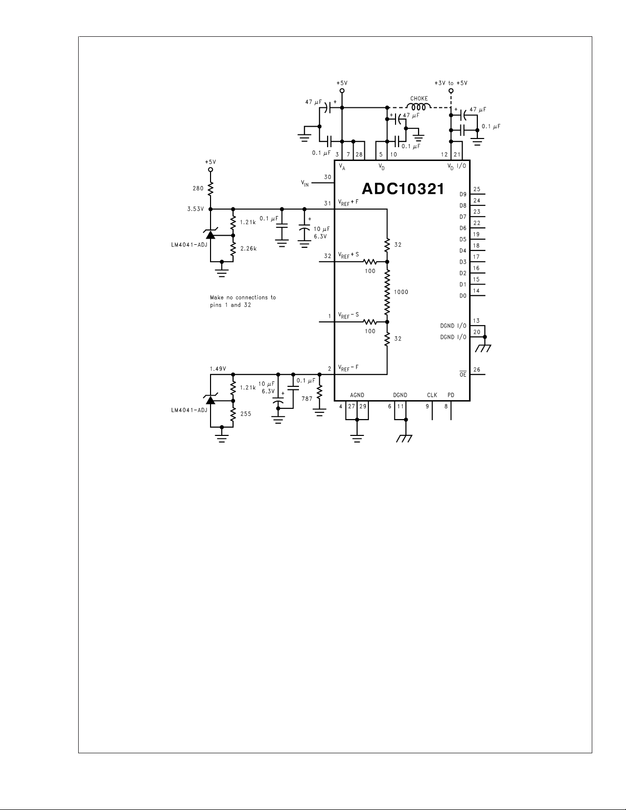
With the addition of two op-amps, the voltages at the top and
bottom of the reference ladder can be forced to the exact
value desired, as shown in Figure 6.
www.national.com 12
Page 13

Applications Information (Continued)
ADC10321
FIGURE 4. Simple, low component count reference biasing
10089718
www.national.com13
Page 14
Applications Information (Continued)
ADC10321
FIGURE 5. Better low component count reference biasing
The V
+ F and V
REF
− F pins should each be bypassed to
REF
AGND with 10µF tantalum or electrolytic and 0.1µF ceramic
capacitors. The circuit of Figure 6 may be used if it is desired
to obtain precise reference voltages. The LMC6082 in this
circuit was chosen for its low offset voltage, low voltage
rail-to-rail capability and low cost.
Since the current flowing through the sense lines (those lines
associated with V
+ S and V
REF
− S) is essentially zero,
REF
there is negligible voltage drop across any resistance in
series with these sense pins and the voltage at the inverting
input of the op-amp accurately represents the voltage at the
top (or bottom) of the ladder. The op-amp drives the force
input, forcing the voltage at the ends of the ladder to equal
the voltage at the op-amp’s non-inverting input, plus any
offset voltage. For this reason, op-amps with low V
OS
, such
as the LMC6081 and LMC6082, should be used for this
application.
10089719
Voltages at the reference sense pins (V
+ S and V
REF
REF
−S)
should be within the range specified in the Operating Ratings
table (2.3V to 4.0V for V
+ and 1.3V to 3.0V for V
REF
REF
−).
Any device used to drive the reference pins should be able to
source sufficient current into the V
cient current from the V
− F pin when the ladder is at its
REF
+ F pin and sink suffi-
REF
minimum value of 850 Ohms.
The reference voltage at the top of the ladder (V
REF
+) may
take on values as low as 1.0V above the voltage at the
bottom of the ladder (V
Volts. The voltage at the bottom of the ladder (V
−) and as high as (VA- 1.0V)
REF
REF
−) may
take on values as low as 1.3 Volts and as high as 3.0V.
However, to minimize noise effects and ensure accurate
conversions, the total reference voltage range (V
−) should be a minimum of 2.0V and a maximum of
V
REF
REF
+-
2.7V.
www.national.com 14
Page 15

Applications Information (Continued)
ADC10321
FIGURE 6. Setting precision reference voltages
3.0 POWER SUPPLY CONSIDERATIONS
A/D converters draw sufficient transient current to corrupt
their own power supplies if not adequately bypassed. A 10µF
to 50µF tantalum or aluminum electrolytic capacitor should
be placed within an inch (2.5 centimeters) of the A/D power
pins, with a 0.1µF ceramic chip capacitor placed as close as
possible to each of the converter’s power supply pins. Leadless chip capacitors are preferred because they have low
lead inductance.
While a single voltage source should be used for the analog
and digital supplies of the ADC10321, this supply should not
be the supply that is used for other digital circuitry on the
board.
As is the case with all high speed converters, the ADC10321
should be assumed to have little high frequency power supply rejection. A clean analog power source should be used.
No pin should ever have a voltage on it that is in excess of
the supply voltages or below ground, not even on a transient
basis. This can be a problem upon application of power to a
10089720
circuit. Be sure that the supplies to circuits driving the CLK,
PD, OE, analog input and reference pins do not come up any
faster than does the voltage at the ADC10321 power pins.
4.0 THE ADC10321 CLOCK
Although the ADC10321 is tested and its performance is
guaranteed with a 20MHz clock, it typically will function with
clock frequencies from 1MHz to 25MHz. Performance is best
if the clock rise and fall times are 5ns or less.
If the CLK signal is interrupted, or its frequency is too low,
the charge on internal capacitors can dissipate to the point
where the accuracy of the output data will degrade. This is
what limits the minimum sample rate.
The duty cycle of the clock signal can affect the performance
of the A/D Converter. Because achieving a precise duty
cycle is difficult, this device is designed to maintain performance over a range of duty cycles. While it is specified and
performance is guaranteed with a 50% clock duty cycle,
performance is typically maintained over a clock duty cycle
range of 45% to 55%.
www.national.com15
Page 16

Applications Information (Continued)
The clock line should be series terminated at the source end
in the characteristic impedance of that line. Use a series
ADC10321
resistor right after the source such that the source impedance plus that series resistor equals the characteristic impedance of the clock line. This resistor should be as close to
the source as possible, but in no case should it be further
away than
where tris the rise time of the clock signal and tPRis the
propagation rate down the board. For a Board of FR-4
material, t
To maintain a consistent impedance along the clock line, use
stripline or microstrip techniques (see Application Note AN-
1113) and avoid the use of through-holes in the line.
It might also be necessary to terminate the ADC end of the
clock line with a series RC to ground such that the resistor
value equals the characteristic impedance of the clock line
and the capacitor value is
is typically about 150 ps/inch.
PR
5.0 LAYOUT AND GROUNDING
Proper routing of all signals and proper ground techniques
are essential to ensure accurate conversion. Separate analog and digital ground planes are required to meet data sheet
limits. The analog ground plane should be low impedance
and free of noise form other parts of the system.
Each bypass capacitor should be located as close to the
appropriate converter pin as possible and connected to the
pin and the appropriate ground plane with short traces. The
analog input should be isolated from noisy signal traces to
avoid coupling of spurious signals into the input. Any external component (e.g., a filter capacitor) connected between
the converter’s input and ground should be connected to a
very clean point in the analog ground return.
Figure 7 gives an example of a suitable layout, including
power supply routing, ground plane separation, and bypass
capacitor placement. All analog circuitry (input amplifiers,
filters, reference components, etc.) should be placed on or
over the analog ground plane. All digital circuitry and I/O
lines should be over the digital ground plane.
Digital and analog signal lines should never run parallel to
each other in close proximity with each other. They should
only cross each other when absolutely necessary, and then
only at 90˚ angles. Violating this rule can result in digital
noise getting into the input, which degrades accuracy and
dynamic performance (THD, SNR, SINAD).
where tPRis again the propagation rate down the clock line,
L is the length of the line in inches and Z
is the character-
O
istic impedance of the clock line.
10089721
FIGURE 7. An acceptable layout pattern
www.national.com 16
Page 17

Applications Information (Continued)
6.0 DYNAMIC PERFORMANCE
The ADC10321 is ac tested and its dynamic performance is
guaranteed. To meet the published specifications, the clock
source driving the CLK input must be free of jitter. For best
ac performance, isolating the ADC clock from any digital
circuitry should be done with adequate buffers, as with a
clock tree. See Figure 8
Meeting dynamic specifications is also dependent upon
keeping digital noise out of the input, as mentioned in Sections 1.0 and 5.0.
10089722
FIGURE 8. Isolating the ADC clock from digital
circuitry
7.0 COMMON APPLICATION PITFALLS Driving the inputs (analog or digital) beyond the power
supply rails. For proper operation, all inputs should not go
more than 300mV beyond the supply pins. Exceeding these
limits on even a transient basis can cause faulty or erratic
operation. It is not uncommon for high speed digital circuits
(e.g., 74F and 74AC devices) to exhibit undershoot that goes
more than a volt below ground. A resistor of 50 to 100Ω in
series with the offending digital input will usually eliminate
the problem.
Care should be taken not to overdrive the inputs of the
ADC10321 (or any device) with a device that is powered
from supplies outside the range of the ADC10321 supply.
Such practice may lead to conversion inaccuracies and even
to device damage.
Attempting to drive a high capacitance digital data bus.
The more capacitance the output drivers has to charge for
each conversion, the more instantaneous digital current is
required from V
and DGND. These large charging current
D
spikes can couple into the analog section, degrading dynamic performance. Adequate bypassing and maintaining
separate analog and digital ground planes will reduce this
problem on the board. Buffering the digital data outputs (with
an 74F541, for example) may be necessary if the data bus to
be driven is heavily loaded. Dynamic performance can also
be improved by adding series resistors of 47Ω at each digital
output.
Driving the V
+ F pin or the V
REF
− F pin with devices
REF
that can not source or sink the current required by the
ladder. As mentioned in section 2.0, be careful to see that
any driving devices can source sufficient current into the
+ F pin and sink sufficient current from the V
V
REF
REF
− F pin.
If these pins are not driven with devices than can handle the
required current, they will not be held stable and the converter output will exhibit excessive noise.
Using a clock source with excessive jitter. This will cause
the sampling interval to vary, causing excessive output noise
and a reduction in SNR performance. Simple gates with RC
timing is generally inadequate.
Using the same voltage source for V
logic. As mentioned in Section 3.0, V
power source used by V
, but should be decoupled from VA.
A
and other digital
D
should use the same
D
ADC10321
www.national.com17
Page 18

Physical Dimensions inches (millimeters) unless otherwise noted
32-Lead TQFP Package
Ordering Number ADC10321CIVT
NS Package Number VBE32A
LIFE SUPPORT POLICY
NATIONAL’S PRODUCTS ARE NOT AUTHORIZED FOR USE AS CRITICAL COMPONENTS IN LIFE SUPPORT
DEVICES OR SYSTEMS WITHOUT THE EXPRESS WRITTEN APPROVAL OF THE PRESIDENT AND GENERAL
COUNSEL OF NATIONAL SEMICONDUCTOR CORPORATION. As used herein:
1. Life support devices or systems are devices or
ADC10321 10-Bit, 20MSPS, 98mW A/D Converter with Internal Sample and Hold
systems which, (a) are intended for surgical implant
into the body, or (b) support or sustain life, and
whose failure to perform when properly used in
accordance with instructions for use provided in the
2. A critical component is any component of a life
support device or system whose failure to perform
can be reasonably expected to cause the failure of
the life support device or system, or to affect its
safety or effectiveness.
labeling, can be reasonably expected to result in a
significant injury to the user.
National Semiconductor
Americas Customer
Support Center
Email: new.feedback@nsc.com
Tel: 1-800-272-9959
www.national.com
National Semiconductor
Europe Customer Support Center
Fax: +49 (0) 180-530 85 86
Email: europe.support@nsc.com
Deutsch Tel: +49 (0) 69 9508 6208
English Tel: +44 (0) 870 24 0 2171
Français Tel: +33 (0) 1 41 91 8790
National Semiconductor
Asia Pacific Customer
Support Center
Fax: 65-6250 4466
Email: ap.support@nsc.com
Tel: 65-6254 4466
National Semiconductor
Japan Customer Support Center
Fax: 81-3-5639-7507
Email: nsj.crc@jksmtp.nsc.com
Tel: 81-3-5639-7560
National does not assume any responsibility for use of any circuitry described, no circuit patent licenses are implied and National reserves the right at any time without notice to change said circuitry and specifications.
 Loading...