

Page 1
January 1995
ADC10154, ADC10158 10-Bit Plus Sign 4 ms ADCs
with 4- or 8-Channel MUX, Track/Hold and Reference
ADC10154, ADC10158 10-Bit Plus Sign 4 ms ADCs with
4- or 8-Channel MUX, Track/Hold and Reference
General Description
The ADC10154 and ADC10158 are CMOS 10-bit plus sign
successive approximation A/D converters with versatile analog input multiplexers, track/hold function and a 2.5V
band-gap reference. The 4-channel or 8-channel multiplexers can be software configured for single-ended, differential
or pseudo-differential modes of operation.
The input track/hold is implemented using a capacitive array and sampled-data comparator.
Resolution can be programmed to be 8-bit, 8-bit plus sign,
10-bit or 10-bit plus sign. Lower-resolution conversions can
be performed faster.
The variable resolution output data word is read in two
bytes, and can be formatted left justified or right justified,
high byte first.
Applications
Y
Process control
Y
Instrumentation
Y
Test equipment
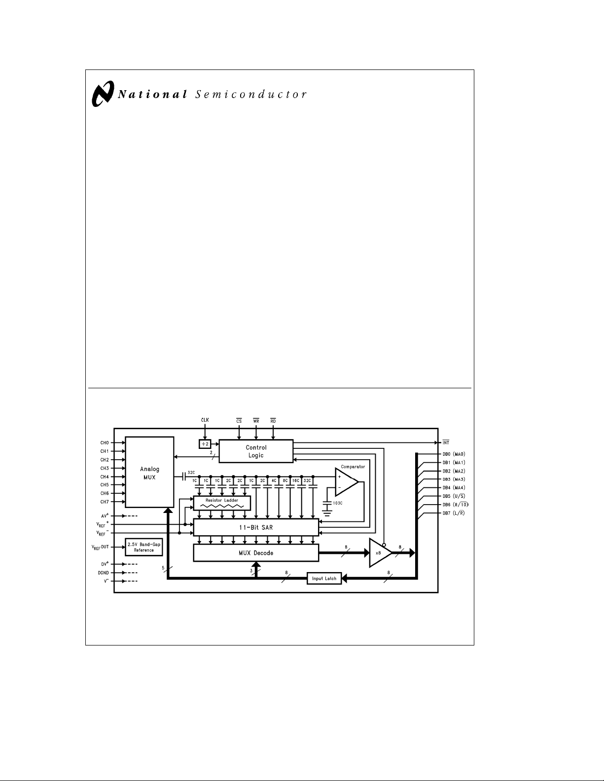
ADC10158 Simplified Block Diagram
Features
Y
4- or 8- channel configurable multiplexer
Y
Analog input track/hold function
Y
0V to 5V analog input range with singlea5V power
supply
Y
b
5V toa5V analog input voltage range withg5V sup-
plies
Y
Fully tested in unipolar (singlea5V supply) and bipolar
g
(dual
Y
Y
Y
Y
Y
5V supplies) operation
Programmable resolution/speed and output data format
Ratiometric or Absolute voltage reference operation
No zero or full scale adjustment required
No missing codes over temperature
Easy microprocessor interface
Key Specifications
Y
Resolution 10-bit plus sign
Y
Integral linearity error
Y
Unipolar power dissipation 33 mW (max)
Y
Conversion time (10-bitasign) 4.4 ms (max)
Y
Conversion time (8-bit) 3.2 ms (max)
Y
Sampling rate (10-bitasign) 166 kHz
Y
Sampling rate (8-bit) 207 kHz
Y
Band-gap reference 2.5Vg2.0% (max)
g
1 LSB (max)
TL/H/11225– 1
TRI-STATEÉis a registered trademark of National Semiconductor Corporation.
C
1995 National Semiconductor Corporation RRD-B30M75/Printed in U. S. A.
TL/H/11225
Page 2
Absolute Maximum Ratings (Notes1&3)
If Military/Aerospace specified devices are required,
please contact the National Semiconductor Sales
Office/Distributors for availability and specifications.
Positive Supply Voltage (V
Negative Supply Voltage (Vb)
Total Supply Voltage (V
Total Reference Voltage (V
Voltage at Inputs and
Outputs V
Input Current at Any Pin (Note 4)
Package Input Current (Note 4)
Package Dissipation at T
ESD Susceptibility (Note 6) 2000V
Soldering Information
N Packages (10 Sec) 260
J Packages (10 Sec) 300
SO Package (Note 7):
Vapor Phase (60 Sec) 215
Infrared (15 Sec) 220
Storage Temperature
Ceramic DIP Packages
Plastic DIP and SO Packages
a
a
e
e
AV
DVa) 6.5V
a
b
Vb) 13V
a
REF
e
25§C (Note 5) 500 mW
A
b
b
V
) 6.6V
REF
b
b
0.3V to V
b
65§Ctoa150§C
b
40§Ctoa150§C
a
b
a
g
g
6.5V
0.3V
5mA
20 mA
§
§
§
§
Operating Ratings (Notes2&3)
Temperature Range T
ADC10154CIN, ADC10154CIWM,
ADC10158CIN, ADC10158CIWM
Positive Supply Voltage
a
a
e
(V
Unipolar Negative Supply
Voltage (V
Bipolar Negative Supply
Voltage (V
a
b
V
V
REF
V
REF
V
REF(VREF
C
C
C
C
a
b
e
AV
DVa) 4.5 VDCto 5.5 V
b
) DGND
b
)
b
V
AV
AV
a
b
b
V
REF
s
s
T
T
A
s
a
85§C
A
4.5V tob5.5V
b
b
0.05 V
b
b
0.05 V
a
a
0.05 VDCto V
a
a
0.05 VDCto V
b
40§CsT
MIN
b
) 0.5 VDCto V
MAX
DC
11V
DC
DC
a
Electrical Characteristics
The following specifications apply for V
unipolar operation or V
apply for T
A
b
e
eb
e
T
T
MIN
to T
J
a
a
e
AV
5.0 VDCfor bipolar operation, and f
; all other limits T
MAX
a
e
ea
DV
e
e
T
A
J
5.0 VDC,V
e
CLK
25§C. (Notes 8, 9, and 12)
Symbol Parameter Conditions
UNIPOLAR CONVERTER AND MULTIPLEXER STATIC CHARACTERISTICS
Resolution 10aSign Bits
a
Unipolar Integral V
Linearity Error V
Unipolar Full-Scale Error V
Unipolar Offset Error V
Unipolar Total Unadjusted V
Error (Note 13) V
Unipolar Power Supply V
Sensitivity V
Offset Error
e
2.5V
REF
a
e
5.0V
REF
a
e
2.5V
REF
a
e
V
V
REF
REF
REF
REF
REF
a
REF
a
a
a
a
ea
a
5.0V
e
2.5V
e
5.0V
e
2.5V
e
5.0V
5Vg10%
e
4.5V
Full-Scale Error
Integral Linearity Error
a
e
5.000 VDC,V
REF
5.0 MHz unless otherwise specified. Boldface limits
REF
b
e
GND, V
b
e
GND for
CIN and CIWM
Typical
(Note 10)
Suffixes
Limits
Units
(Limit)
(Note 11)
g
0.5 LSB
g
0.5 LSB
g
1 LSB
g
1.5 LSB
g
0.25
g
0.25
g
0.25 LSB
g
1 LSB (Max)
g
1.5 LSB (Max)
g
1.5 LSB (Max)
g
2 LSB (Max)
g
1 LSB (Max)
g
1 LSB (Max)
2
Page 3
Electrical Characteristics
The following specifications apply for V
unipolar operation or V
apply for T
A
Symbol Parameter Conditions
b
e
eb
e
T
T
J
MIN
a
a
e
AV
5.0 VDCfor bipolar operation, and f
to T
; all other limits T
MAX
a
e
ea
DV
e
A
a
5.0 VDC,V
e
CLK
e
T
25§C. (Notes 8, 9, and 12) (Continued)
J
e
5.000 VDC,V
REF
5.0 MHz unless otherwise specified. Boldface limits
Typical
(Note 10)
BIPOLAR CONVERTER AND MULTIPLEXER STATIC CHARACTERISTICS
Resolution 10aSign Bits
a
Bipolar Integral V
Linearity Error
Bipolar Full-Scale Error V
Bipolar Negative Full-Scale V
Error with Positive-Full
REF
REF
REF
e
5.0V
a
e
5.0V
a
e
5.0V
Scale Adjusted
a
Bipolar Offset Error V
Bipolar Total Unadjusted V
Error (Note 13)
REF
REF
e
5.0V
a
e
5.0V
Bipolar Power Supply
Sensitivity
Offset Error V
Full-Scale Error V
Integral Linearity Error
Offset Error V
Full-Scale Error V
Integral Linearity Error
a
REF
b
REF
ea
a
eb
a
5Vg10%
e
4.5V
5Vg10%
e
4.5V
g
0.5
g
0.5
g
0.25 LSB
g
0.25
g
0.25
g
0.25 LSB
UNIPOLAR AND BIPOLAR CONVERTER AND MULTIPLEXER STATIC CHARACTERISTICS
Missing Codes 0
a
b
DC Common Mode V
Error (Note 14)
Bipolar
Unipolar
R
REF
C
REF
V
AI
C
AI
Reference Input Resistance 7 4.5 kX (Max)
Reference Input Capacitance 70 pF
Analog Input Voltage (V
Analog Input Capacitance 30 pF
Off Channel Leakage On Channele5V
IN
e
VINwhere
a
5.0VtV
a
5.0VtV
e
V
IN
t
b
5.0V
IN
t
0V
IN
g
0.25
g
0.25
b
400
Current Off Channele0V
(Note 15)
On Channele0V 400 1000 nA (Max)
Off Channel
e
5V
b
e
GND, V
REF
CIN and CIWM
Suffixes
Limits
(Note 11)
g
1 LSB (Max)
g
1.25 LSB (Max)
g
1.25 LSB (Max)
g
2.5 LSB (Max)
g
3 LSB (Max)
g
2.5 LSB (Max)
g
1.5 LSB (Max)
g
0.75 LSB (Max)
g
0.75 LSB (Max)
g
0.75 LSB (Max)
g
0.5 LSB (Max)
9.5 kX (Max)
a
a
0.05) V (Max)
b
b
(V
0.05) V (Min)
b
1000 nA (Max)
b
e
GND for
Units
(Limit)
3
Page 4
Electrical Characteristics
The following specifications apply for V
unipolar operation or V
apply for T
A
Symbol Parameter Conditions
b
e
eb
e
T
T
MIN
to T
J
a
a
e
AV
5.0 VDCfor bipolar operation, and f
; all other limits T
MAX
a
e
ea
DV
e
e
T
A
J
a
5.0 VDC,V
e
CLK
25§C. (Notes 8, 9, and 12) (Continued)
e
5.000 VDC,V
REF
5.0 MHz unless otherwise specified. Boldface limits
REF
Typical
(Note 10)
b
e
Limits
(Note 11)
GND, V
DYNAMIC CONVERTER AND MULTIPLEXER CHARACTERISTICS
S/(NaD) Unipolar Signal-to-Noise
a
Distortion Ratio f
S/(NaD) Bipolar Signal-to-Noise
a
Distortion Ratio f
b
3 dB Unipolar Full V
Power Bandwidth
b
3 dB Bipolar Full V
Power Bandwidth
REFERENCE CHARACTERISTICS (Unipolar Operation V
V
Out Reference Output Voltage 2.5g1% 2.5g2% V (Max)
REF
DV
/DtV
REF
DV
/DILLoad Regulation Sourcing 0 mAsI
REF
Out Temperature Coefficient 40 ppm/§C
REF
Sinking 0 mAtI
Line Regulation 4.5VsV
I
DV
t
SC
REF
SU
Short Circuit Current V
/Dt Long-Term Stability 200 ppm/1 kHr
Start-Up Time C
e
f
10 kHz, V
IN
e
150 kHz, V
IN
e
f
10 kHz, V
IN
e
150 kHz, V
IN
e
4.85 V
IN
e
g
IN
b
e
GND Only)
Oute0V 14 25 mA (Max)
REF
e
330 mF20 ms
L
e
4.85 V
IN
IN
IN
IN
p–p
p–p
e
4.85 V
e
g
4.85V 60 dB
e
g
4.85V 58 dB
4.85V
s
a
4 mA 0.003 0.1 %/mA (Max)
L
t
b
1 mA 0.2 0.6 %/mA (Max)
L
a
s
5.5V 0.5 6 mV (Max)
60 dB
58 dB
p-p
200 kHz
200 kHz
DIGITAL AND DC CHARACTERISTICS
a
V
IN(1)
V
IN(0)
I
IN(1)
I
IN(0)
V
OUT(1)
V
OUT(0)
I
OUT
a
b
DI
AI
b
I
I
REF
Logical ‘‘1’’ Input Voltage V
Logical ‘‘0’’ Input Voltage V
Logical ‘‘1’’ Input Current V
Logical ‘‘0’’ Input Current V
Logical ‘‘1’’ Output Voltage V
Logical ‘‘0’’ Output Voltage V
TRI-STATEÉOutput Current V
I
SC
I
SC
a
a
Output Short Circuit Source Current V
Output Short Circuit V
Sink Current
Digital Supply Current CSeHIGH 0.75 2 mA (Max)
Analog Supply Current CSeHIGH 3 4.5 mA (Max)
Negative Supply Current CSeHIGH 3.5 4.5 mA (Max)
Reference Input Current V
e
5.5V 2.0 V (Min)
a
e
4.5V 0.8 V (Max)
e
5.0V 0.005 2.5 mA (Max)
IN
e
0V
IN
a
e
4.5V:
a
e
4.5V
e
I
1.6 mA
OUT
e
0V
OUT
e
V
5V 0.01 3 mA (Max)
OUT
e
0V
OUT
e
DV
OUT
CSeHIGH, f
CSeHIGH, f
CSeHIGH, f
a
e
REF
eb
I
OUT
I
OUT
a
CLK
CLK
CLK
360 mA 2.4 V (Min)
eb
10 mA 4.25 V (Min)
e
0 Hz 0.15 mA (Max)
e
0 Hz 3 mA (Max)
e
0 Hz 3.5 mA (Max)
5V 0.7 1.1 mA (Max)
b
0.005
b
2.5 mA (Max)
0.4 V (Max)
b
0.01
b
40
b
3 mA (Max)
b
10 mA (Min)
30 10 mA (Min)
b
e
GND for
(Limit)
Units
4
Page 5
Electrical Characteristics
The following specifications apply for V
for unipolar operation or V
Boldface limits apply for T
b
eb
A
a
a
e
e
AV
5.0 VDCfor bipolar operation, t
e
e
T
T
J
MIN
to T
MAX
DV
; all other limits T
a
ea
5.0 VDC,V
e
t
r
f
Symbol Parameter Conditions
AC CHARACTERISTICS
f
CLK
Clock Frequency 8 5.0 MHz (Max)
Clock Duty Cycle 20 % (Min)
t
C
Conversion 8-Bit Unipolar Mode 16 1/f
Time
f
CLK
e
8-Bit Bipolar Mode 18 1/f
e
f
CLK
10-Bit Unipolar Mode 20 1/f
e
f
CLK
10-Bit Bipolar Mode 22 1/f
e
f
CLK
t
A
t
CR
t
RC
t
CW
t
WC
t
RW
t
W(WR)
t
WS
t
DS
t
DH
t
WR
t
ACC
tWI,t
t
INTL
Acquisition Time 6 1/f
e
f
CLK
Delay between Falling Edge of
CS
and Falling Edge of RD
Delay betwee Rising Edge
RD and Rising Edge of CS
Delay between Falling Edge
of CS
and Falling Edge of WR
Delay between Rising Edge
of WR
and Rising Edge of CS
Delay between Falling Edge
of RD
and Falling Edge of WR
WR Pulse Width 25 50 ns (Min)
WR High to CLKd2 Low Set-Up Time 5 ns (Max)
Data Set-Up Time 6 15 ns (Max)
Data Hold Time 0 5 ns (Max)
Delay from Rising Edge
of WR to Rising Edge RD
Access Time (Delay from Falling C
Edge of RD
Delay from Falling Edge C
RI
of WR
to Output Data Valid)
or RD to Reset of INT
e
L
e
L
Delay from Falling Edge of CLKd2 to Falling
Edge of INT
e
3 ns and f
e
A
ae
REF
5.000 VDC,V
e
5.0 MHz unless otherwise specified.
CLK
e
T
25§C. (Note 16) (Continued)
J
Typical
(Note 10)
be
REF
Limits
(Note 11)
GND, V
b
(Limit)
e
Units
10 kHz (Min)
80 % (Max)
5.0 MHz 3.2 ms (Max)
5.0 MHz 3.6 ms (Max)
5.0 MHz 4.0 ms (Max)
5.0 MHz 4.4 ms (Max)
5.0 MHz 1.2 ms
0 5
ns (Min)
0 5 ns (Min)
0 5 ns (Min)
0 5 ns (Min)
0 5 ns (Min)
0 5 ns (Min)
100 pF
100 pF
25 45 ns (Max)
25 40 ns (Max)
40 ns
GND
CLK
CLK
CLK
CLK
CLK
5
Page 6
Electrical Characteristics
The following specifications apply for V
for unipolar operation or V
Boldface limits apply for T
Symbol Parameter Conditions
b
eb
A
a
a
e
e
AV
5.0 VDCfor bipolar operation, t
e
e
T
T
J
MIN
to T
MAX
DV
; all other limits T
a
ea
5.0 VDC,V
e
e
t
r
f
REF
3 ns and f
e
T
A
ae
5.000 VDC,V
e
CLK
e
25§C. (Note 16) (Continued)
J
REF
5.0 MHz unless otherwise specified.
Typical
(Note 10)
be
GND, V
Limits
(Note 11)
b
AC CHARACTERISTICS (Continued)
t1H,t
t
RR
t
P
TRI-STATE Control (Delay from C
0H
Rising Edge of RD
to Hi-Z State)
Delay between Successive
RD
Pulses
Delay between Last Rising Edge
of RD
and the Next Falling 20 50 ns (Min)
L
e
10 pF, R
e
1kX
L
20 35 ns (Max)
25 50 ns (Min)
Edge of WR
C
IN
C
OUT
Note 1: Absolute Maximum Ratings indicate limits beyond which damage to the device may occur.
Note 2: Operating Ratings indicate conditions for which the device is functional, but do not guarantee specific performance limits. For guaranteed specifications
and test conditions, see the Electrical Characteristics. The guaranteed specifications apply only for the test conditions listed. Some performance characteristics
may degrade when the device is not operated under the listed test conditions.
Note 3: All voltages are measured with respect to GND, unless otherwise specified.
Note 4: When the input voltage (V
The 20 mA maximum package input current rating limits the number of pins that can safely exceed the power supplies with an input current of 5 mA to four.
Note 5: The maximum power dissipation must be derated at elevated temperatures and is dictated by T
allowable power dissipation at any temperature is P
device, T
with BIJ, CIJ and CMJ suffixes 49
and CMJ suffixes 46
Note 6: Human body model, 100 pF capacitor discharged through a 1.5 kX resistor.
Note 7: See AN-450 ‘‘Surface Mounting Methods and Their Effect on Product Reliability’’ or the section titled ‘‘Surface Mount’’ found in any post-1986 National
Semiconductor Linear Data Book for other methods of soldering surface mount devices.
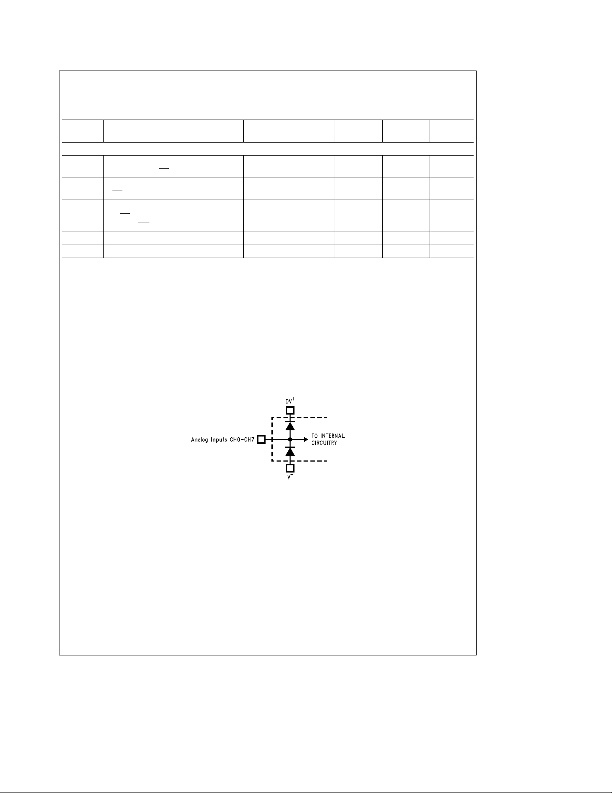
Note 8: Two on-chip diodes are tied to each analog input as shown below. They will forward-conduct for analog input voltages one diode drop below V
Capacitance of Logic Inputs 5 pF
Capacitance of Logic Outputs 5 pF
) at any pin exceeds the power supplies (V
IN
e
b
(T
e
150§C. The typical thermal resistance (iJA) of these parts when board mounted follow: ADC10154 with BIN and CIN suffixes 65§C/W, ADC10154
Jmax
C/W, ADC10158 with BIWM and CIWM suffixes 68§C/W.
§
C/W, ADC10154 with BIWM and CIWM suffixes 72§C/W, ADC10158 with BIN and CIN suffixes 59§C/W, ADC10158 with BIJ, CIJ,
§
D
TA)/iJAor the number given in the Absolute Maximum Ratings, whichever is lower. For this
Jmax
k
IN
Vbor V
l
AVaor DVa), the current at that pin should be limited to 5 mA.
IN
, iJAand the ambient temperature, TA. The maximum
Jmax
b
e
GND
Units
(Limit)
supply or
one diode drop greater than Vasupply. Be careful during testing at low Valevels (4.5V), as high level analog inputs (5V) can cause an input diode to conduct,
especially at elevated temperatures, which will cause errors for analog inputs near full-scale. The specification allows 50 mV forward bias of either diode; this
means that as long as the analog V
unselected channel will corrupt the reading of a selected channel. This means that if AV
scale must be
s
g
4.55 VDC.
does not exceed the supply voltage by more than 50 mV, the output code will be correct. Exceeding this range on an
IN
a
and DVaare minimum (4.5 VDC) and Vbis a maximum (b4.5 VDC) full
TL/H/11225– 4
6
Page 7
Electrical Characteristics (Continued)
Note 9: A diode exists between AVaand DVaas shown below.
To guarantee accuracy, it is required that the AVaand DVabe connected together to a power supply with separate bypass filter at each Vapin.
Note 10: Typicals are at T
Note 11: Tested limits are guaranteed to National’s AOQL (Average Outgoing Quality Level).
Note 12: One LSB is referenced to 10 bits of resolution.
Note 13: Total unadjusted error includes offset, full-scale, linearity, multiplexer, and hold step errors.
Note 14: For DC Common Mode Error the only specification that is measured is offset error.
Note 15: Channel leakage current is measured after the channel selection.
Note 16: All the timing specifications are tested at the TTL logic levels, V
e
e
T
25§C and represent most likely parametric norm.
J
A
e
0.8V for a falling edge and V
IL
TL/H/11225– 5
e
2.0V for a rising.
IH
Ordering Information
Industrialb40§CsT
ADC10154CIN N24A
ADC10154CIWM M24B
ADC10158CIN N28B
ADC10158CIWM M28B
s
85§C Package
A
7
Page 8
Electrical Characteristics (Continued)
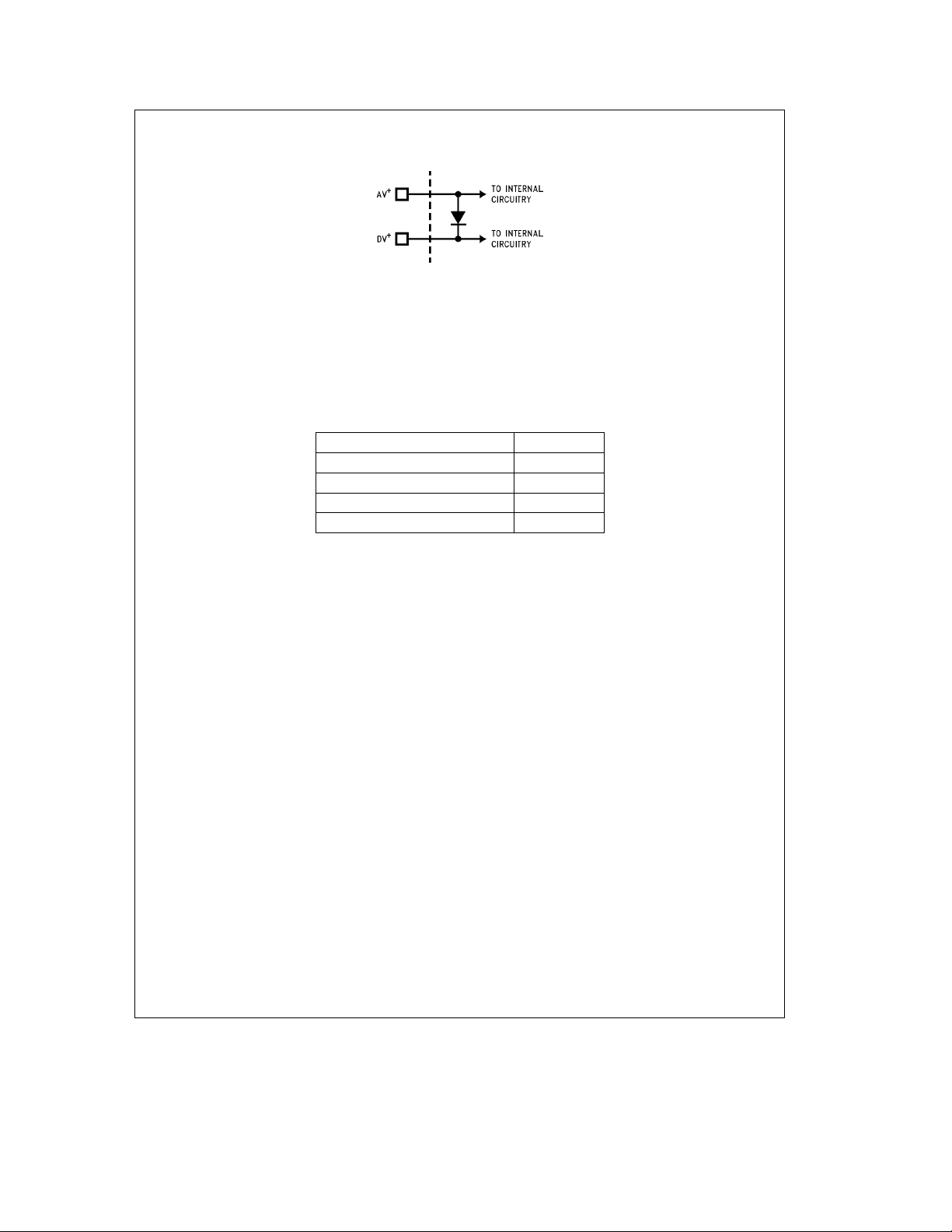
FIGURE 1A. Transfer Characteristic
FIGURE 1B. Simplified Error Curve vs Output Code
TL/H/11225– 6
TL/H/11225– 7
8
Page 9

Typical Converter Performance Characteristics
Total Positive Supply
Current (DI
a
a
AIa)
vs Temperature
Offset Error vs
Reference Voltage
Linearity Error vs
Clock Frequency
Total Positive Power
Supply Current (DI
a
a
vs Clock Frequency
Linearity Error
vs Temperature
Spectral Response with
50 kHz Sine Wave
AIa)
Offset Error
vs Temperature
Linearity Error vs
Reference Voltage
10-Bit Unsigned
Signal-to-Noise
a
vs Input Signal Level
THD Ratio
TL/H/11225– 8
9
Page 10

Typical Reference Performance Characteristics
Load Regulation (3 Typical Parts)
Line Regulation
Available
Output Current
vs Supply Voltage
Output Drift
vs Temperature
(3 Typical Parts)
TL/H/11225– 9
10
Page 11

Leakage Current Test Circuit
TRI-STATE Test Circuits and Waveforms
TL/H/11225– 11
TL/H/11225– 10
TL/H/11225– 12
TL/H/11225– 13
TL/H/11225– 14
11
Page 12

Timing Diagrams
DIAGRAM 1. Starting a Conversion with New MUX Channel and Output Configuration
DIAGRAM 2. Starting a Conversion without Changing the MUX Channel or Output Configuration
TL/H/11225– 15
TL/H/11225– 16
12
Page 13

Timing Diagrams (Continued)
DIAGRAM 3. Reading the Conversion Result
TL/H/11225– 17
Multiplexer Addressing and Output Data Configuration Tables
TABLE I. ADC10154 and ADC10158 Output Data Configuration
Resolution Data
10-BitsaSign Right-Justified L L L Sign Sign Sign Sign Sign Sign MSB 9 First Byte Read
10-BitsaSign Left-Justified L L H Sign MSB 9 8 7 6 5 4 First Byte Read
10-Bits Right-Justified L H L L L L L L L MSB 9 First Byte Read
10-Bits Left-Justified L H H MSB 9 8 7 6 5 4 3 First Byte Read
8-BitsaSign Right-Justified H L L Sign Sign Sign Sign Sign Sign Sign Sign First Byte Read
8-BitsaSign Left-Justified H L H Sign MSB 7 6 5 4 3 2 First Byte Read
8-Bits Right-Justified H H L L L L L L L L L First Byte Read
8-Bits Left-Justified H H H MSB 7 6 5 4 3 2 LSB First Byte Read
Output
Data Format
Control Input
8/10 U/S L/R DB7 DB6 DB5 DB4 DB3 DB2 DB1 DB0
8 7 6 5 4 3 2 LSB Second Byte Read
3 2 LSB L L L L L Second Byte Read
8 7 6 5 4 3 2 LSB Second Byte Read
2 LSB L L L L L L Second Byte Read
MSB 7 6 5 4 3 2 LSB Second Byte Read
LSB L L L L L L L Second Byte Read
MSB 7 6 5 4 3 2 LSB Second Byte Read
L L L L L L L L Second Byte Read
Data Bus Output Assignment
13
Page 14

Multiplexer Addressing and Output Data Configuration Tables (Continued)
TABLE II. ADC10158 Multiplexer Addressing
MUX Address
CS
WR RD
MA4 MA3 MA2 MA1 MA0 CH0 CH1 CH2 CH3 CH4 CH5 CH6 CH7 V
XLLLLL H
XLLLHL H
ab
ba
XLLHLL H
XLLHHL£H
XLHLLL H
XLHLHL H
XLHHLL H
XLHHHL H
LHLLLL H
LHLLHL H
ab
ab
LHLHLL H
LHLHHL£H
LHHLLL H
LHHLHL H
LHHH LL H
LHHHHL H
HHLLLL H
HHL LHL H
ab
ab
HHLHLL H
HHLHHL£H
HHHL LL H
HHHLHL H
HHHHLL H
XXXXXL£L Previous Channel Configuration
Channel Number
b
REF
ab
ba
ab
ab
ab
ba
ab
ba
ab
ab
ab
ab
ab
ab
ab
ab
ab
MUX
Mode
Differential
Single-Ended
Pseudo-Differential
TABLE III. ADC10154 Multiplexer Addressing
MUX Address
CS
WR RD
Channel Number
MA4 MA3 MA2 MA1 MA0 CH0 CH1 CH2 CH3 V
XXL LLL H
XXL LHL
XXLHLL H
£
XXLHHL H
XLHLLL H
XLHLHL
XLHHLL H
£
XLHHHL H
XHHL LL H
XHHLHL£H
XHHHLL H
ab
ba
H
ab
H
ab
ab
ba
ab
ab
ab
ab
ab
XXXXXL£L Previous Channel Configuration
14
REF
b
MUX
Mode
Differential
Single-Ended
Pseudo-Differential
Page 15

Detailed Block Diagram
TL/H/11225– 18
15
Page 16

Connection Diagrams
Dual-In Line and SO Packages
Top View
TL/H/11225– 2
Order Number ADC10154
NS Package Numbers
J24A, M24B or N24A
1.0 Pin Descriptions
a
AV
DV
DGND This is the digital ground. All logic levels are
b
V
V
REF
V
REF
V
REF
CS
This is the positive analog supply. This pin
should be bypassed with a 0.1 mF ceramic capacitor and a 10 mF tantalum capacitor to the
system analog ground.
a
This is the positive digital supply. This supply
pin also needs to be bypassed with 0.1 mF ceramic and 10 mF tantalum capacitors to the
system digital ground. AV
a
and DVashould
be bypassed separately and tied to same power supply.
referred to this ground.
This is the negative analog supply. For unipolar
operation this pin may be tied to the system
analog ground or to a negative supply source.
It should not go above DGND by more than
50 mV. When bipolar operation is required, the
voltage on this pin will limit the analog input’s
negative voltage level. In bipolar operation this
supply pin needs to be bypassed with 0.1 mF
ceramic and 10 mF tantalum capacitors to the
system analog ground.
a
, These are the positive and negative reference
b
inputs. The voltage difference between V
and V
span.
b
will set the analog input voltage
REF
Out This is the internal band-gap voltage reference
output. For proper operation of the voltage reference, this pin needs to be bypassed with a
330 mF tantalum or electrolytic capacitor.
This is the chip select input. When a logic low is
applied to this pin the WR
and RD pins are
enabled.
REF
Top View
TL/H/11225– 3
Order Number ADC10158
NS Package Numbers
J28A, M28B or N28B
RD
This is the read control input. When a logic low
is applied to this pin the digital outputs are enabled and the INT
output is reset high.
WR This is the write control input. The rising edge
of the signal applied to this pin selects the multiplexer channel and initiates a conversion.
INT
This is the interrupt output. A logic low at this
output indicates the completion of a conversion.
CLK This is the clock input. The clock frequency di-
rectly controls the duration of the conversion
time (for example, in the 10-bit bipolar mode
t
6/f
e
22/f
C
CLK
) and the acquisition time (t
CLK
).
e
A
DB0(MA0)– These are the digital data inputs/outputs. DB0
DB7 (L/R
) is the least significant bit of the digital output
word; DB7 is the most significant bit in the digital output word (see the Output Data Configuration table). MA0 through MA4 are the digital
inputs for the multiplexer channel selection
(see the Multiplexer Addressing tables). U/S
(Unsigned/Signed), 8/10, (8/10-bit resolution)
and L/R
a
(Left/Right justification) are the digital
input bits that set the A/D’s output word format
and resolution (see the Output Data Configuration table). The conversion time is modified by
the chosen resolution (see Electrical AC Characteristics table). The lower the resolution, the
faster the conversion will be.
CH0–CH7 These are the analog input multiplexer chan-
nels. They can be configured as single-ended
inputs, differential input pairs, or pseudo-differential inputs (see the Multiplexer Addressing
tables for the input polarity assignments).
16
Page 17

2.0 Functional Description
The ADC10154 and ADC10158 use successive approximation to digitize an analog input voltage. Additional logic has
been incorporated in the devices to allow for the programmability of the resolution, conversion time and digital output
format. A capacitive array and a resistive ladder structure
are used in the DAC portion of the A/D converters. The
structure of the DAC allows a very simple switching scheme
to provide a very versatile analog input multiplexer. Also,
inherent in this structure is a sample/hold. A 2.5V CMOS
band-gap reference is also provided on the ADC10154 and
ADC10158.
2.1 DIGITAL INTERFACE
The ADC10154 and ADC10158 have eight digital outputs
(DB0–DB8) and can be easily interfaced to an 8-bit data
bus. Taking CS
data word on the data-bus into the input latch. This word will
be decoded to determine the multiplexer channel selection,
the A/D conversion resolution and the output data format.
The following table shows the input word data-bit assignment.
DB0 DB1 DB2 DB3 DB4 DB5 DB6 DB7
MA0 MA1 MA2 MA3 MA4 U/S 8/10 L/R
and WR low simultaneously will strobe the
X ä YX ä Y
MUX Address Control
DB0 through DB4 are assigned to the multiplexer address
data bits zero through four (MA0–MA4). Tables II and III
describe the multiplexer address assignment. DB5 selects
unsigned or signed (U/S
resolution. DB7 selects left or right justification of the output
data. Refer to Table I for the effect the Control Input Data
has on the digital output word.
The conversion process is started by the rising edge of WR
which sets the ‘‘start conversion’’ bit inside the ADC. If this
bit is set, the converter will start acquiring the input voltage
on the next falling edge of the internal CLK
acquisition period is 3 CLK
Immediately after the acquisition period the input signal is
) operation. DB6 selects 8- or 10-bit
d
2 periods, or 6 CLK periods.
Input Data
d
2 signal. The
held and the actual conversion begins. The number of
clocks required for a conversion is given in the following
table:
d
2 CLK
Conversion Type
8-Bit 8 16
8-BitaSign 9 18
10-Bit 10 20
10-BitaSign 11 22
Since the CLKd2 signal is internal to the ADC, it is initially
impossible to know which falling edge of CLK corresponds
to the falling edge of CLK
rising edge of WR
falling edge of CLK. If this edge happens to be on the rising
edge of CLK
version time. The phase of the CLK
mined at the end of the first conversion, when INT
INT
always goes low on the falling edge of the CLKd2 signal. From the first falling edge of INT
falling edge of CLK will correspond to the falling edge of
d
CLK
2. With the phase of CLKd2 now known, the conversion time can be minimized by taking WR
ns before the falling edge of CLKd2.
Upon completion of the conversion, INT goes low to signal
the A/D conversion result is ready to be read. Taking CS
and RD low will enable the digital output buffer and put byte
1 of the conversion result on DB0 through DB7. The falling
edge of RD
low a second time will put byte 2 of the conversion result on
DB7–DB0. Table I defines the DB0 – DB7 assignement for
different Control Input Data. The second read does not have
,
to be completed before a new conversion is started.
Taking CS
version without changing the multiplexer channel assignment or output configuration and resolution. The timing diagram in
Figure 2
ment this function. Refer to Diagrams 1, 2, and 3 in the
Timing Diagrams section for the timing constraints that must
be met.
should occur at least tWSns before any
d
2, this will add 2 CLK cycles to the total con-
resets the INT output high. Taking CS and RD
,WRand RD low simultaneously will start a con-
shows the sequence of events that imple-
CLK
Cycles Cycles (N)
d
2. For the first conversion, the
d
2 signal can be deter-
onward, every other
goes low.
high at least t
WS
FIGURE 2. Starting a Conversion without Updating the Channel Configuration, Resolution, or Data Format
17
TL/H/11225– 19
Page 18

2.0 Functional Description (Continued)
Digital Interface Hints:
Reads and writes can be completely asynchronous to
#
CLK.
In addition to the timing indicated in Diagrams 1 –3, CS
#
can be tied low permanently or taken low for entire conversions, eliminating all the CS
t
).
CW,tWC
If CS is used as shown in Diagrams 1–3, the CS guard-
#
bands (t
CR,tRC,tCW,tWC
WR
signals can safely be ignored as long as the following
two conditions are met:
1) When initiating a write, CS
neously low for at least t
The ‘‘start’’ conversion’’ bit will be set on the rising
edge of WR
or CS, whichever is first.
2) When reading data, understand that data will not be
valid until t
output data will enter TRI-STATE t
either
ns after
ACC
CS or RD goes high (see Diagrams 2 and 3).
2.2 ARCHITECTURE
Before a conversion is started, during the analog input sampling period, the sampled data comparator is zeroed. As the
comparator is being zeroed the channel assigned to be the
positive input is connected to the A/D’s input capacitor.
(See the Digital Interface section for a description of the
assignment procedure.) This charges the input 32C capacitor of the DAC to the positive analog input voltage. The
switches shown in the DAC portion of the detailed block
diagram are set for this zeroing/acquisition period. The voltage at the input and output of the comparator are at equilibrium at this point in time. When the conversion is started the
comparator feedback switches are opened and the 32C input capacitor is then switched to the assigned negative input voltage. When the comparator feedback switch opens a
fixed amount of charge is trapped on the common plates of
the capacitors. The voltage at the input of the comparator
moves away from equilibrium when the 32C capacitor is
switched to the assigned negative input voltage, causing the
output of the comparator to go high (‘‘1’’) or low (‘‘0’’). The
SAR next goes through an algorithm, controlled by the output state of the comparator, that redistributes the charge on
the capacitor array by switching the voltage on one side of
the capacitors in the array. The objective of the SAR algorithm is to return the voltage at the input of the comparator
as close as possible to equilibrium.
4 Single-Ended 2 Differential 3 Pseudo-Differential
guardbands (tCR,tRC,
) between CS and the RD and
and WR must be simulta-
ns (see Diagram 1).
W(WR)
both
CS and RD go low. The
ns or t0Hns after
1H
The switch position information at the completion of the
successive approximation routine is a direct representation
of the digital output. This information is then manipulated by
the Digital Output decoder to the programmed format. The
reformatted data is then available to be strobed onto the
data bus (DB0 –DB7) via the digital output buffers by taking
CS
and RD low.
3.0 Applications Information
3.1 MULTIPLEXER CONFIGURATION
The design of these converters utilizes a sampled-data
comparator structure which allows a differential analog input
to be converted by the successive approximation routine.
The actual voltage converted is always the difference between an assigned ‘‘
minal. The polarity of each input terminal or pair of input
terminals being converted indicates which line the converter
expects to be the most positive. If the assigned ‘‘
less than the ‘‘
zeros output code when configured for unsigned operation.
When configured for signed operation the A/D responds
with the appropriate output digital code.
A unique input multiplexing scheme has been utilized to provide multiple analog channels. The input channels can be
software configured into three modes: differential, singleended, or pseudo-differential.
modes using the 4-channel MUX of the ADC10154. The
eight inputs of the ADC10158 can also be configured in any
of the three modes. The single-ended mode has CH0–CH3
assigned as the positive input with the negative input being
the V
ADC10154 channel inputs are grouped in pairs, CH0 with
REF
b
CH1 and CH2 with CH3. The polarity assignment of each
channel in the pair is interchangeable. Finally, in the pseudo-differential mode CH0 –CH2 are positive inputs referred
to CH3 which is now a pseudo-ground. This pseudo-ground
input can be set to any potential within the input commonmode range of the converter. The analog signal conditioning
required in transducer-based data acquisition systems is
significantly simplified with this type of input flexibility. One
converter package can now handle ground-referred inputs
and true differential inputs as well as signals referred to a
specific voltage.
The analog input voltages for each channel can range from
50 mV below V
b
5V for bipolar operation) to 50 mV above V
AVa(typically 5V) without degrading conversion accuracy.
If the voltage on an unselected channel exceeds these limits it may corrupt the reading of the selected channel.
a
’’ input terminal and a ‘‘b’’ input ter-
a
b
’’ input the converter responds with an all
Figure 3
’’ input is
shows the three
of the device. In the differential mode, the
b
(typically ground for unipolar operation or
a
a
e
DV
2 Single Ended
and 1 Differential
e
FIGURE 3. Analog Input Multiplexer Options
18
TL/H/11225– 20
Page 19

3.0 Applications Information (Continued)
3.2 REFERENCE CONSIDERATIONS
The voltage difference between the V
puts defines the analog input voltage span (the difference
between V
is the programmed resolution) possible output codes apply.
In the pseudo-differential and differential modes the actual
voltage applied to V
tween the AV
importance. When using the single-ended multiplexer mode
the voltage at V
determines the ‘‘zero’’ reference voltage and, with V
(Max) and VIN(Min)) over which the 2n(where n
IN
a
and V
REF
a
and Vb. Only the difference voltage is of
b
has a dual function. It simultaneously
REF
REF
the analog voltage span.
The value of the voltage on the V
can be anywhere between AV
b
50 mV, so long as V
ADC10154 and ADC10158 can be used in either ratiometric
a
is greater than V
REF
applications or in systems requiring absolute accuracy. The
reference pins must be connected to a voltage source capable of driving the minimum reference input resistance of
4.5 kX.
The internal 2.5V bandgap reference in the ADC10154 and
ADC10158 is available as an output on the V
ensure optimum performance this output needs to be bypassed to ground with 330 mF aluminum electrolytic or tantalum capacitor. The reference output is unstable with capacitive loads greater than 100 pF and less than 100 mF.
Any capacitive loads
s
100 pF ort100 mF will not cause
the reference to oscillate. Lower output noise can be obtained by increasing the output capacitance. The 330 mF
a
and V
REF
b
can lie anywhere be-
a
or V
REF
a
REF
a
50 mV and V
REF
b
REF
REF
b
inputs
b
. The
REF
Out pin. To
in-
a
capacitor will yield a typical noise floor of 200 nVrms/
The 2.5V reference output is referred to the negative supply
b
pin (V
). Therefore, the voltage at V
be 2.5V greater than the voltage applied to V
this voltage to V
analog voltage span of 2.5V. In bipolar operation the voltage at V
REF
For the single-ended multiplexer mode the analog input voltage range will be from
REF
a
with V
b
tied to Vbwill yield an
REF
Out will be atb2.5V when Vbis tied tob5V.
b
5V tob2.5V. The pseudo-differential and differential multiplexer modes allow for more flexibility in the analog input voltage range since the ‘‘zero’’ refer-
,
ence voltage is set by the actual voltage applied to the assigned negative input pin. The drawback of using the internal reference in the bipolar mode is that any noise on the
b
b
5V tied to the Vbpin will affect the conversion result. The
bandgap reference is specified and tested in unipolar operation with V
In a ratiometric system
b
tied to the system ground.
(Figure 4a)
, the analog input voltage
is proportional to the voltage used for the A/D reference.
This voltage may also be the system power supply, so
a
V
can also be tied to AVa. This technique relaxes the
REF
stablity requirements of the system reference as the analog
input and A/D reference move together maintaining the
same output code for a given input condition.
For absolute accuracy
(Figure 4b)
, where the analog input
varies between very specific voltage limits, the reference pin
can be biased with a time- and temperature-stable voltage
source that has excellent initial accuracy. The LM4040 and
LM185 references are suitable for use with the ADC10154
and ADC10158.
Out will always
REF
b
Hz.
0
. Applying
a. Ratiometric Using the Internal Reference
TL/H/11225– 21
FIGURE 4. Different Reference Configurations
b. Absolute Using a 4.096V Span
TL/H/11225– 22
19
Page 20

3.0 Applications Information (Continued)
a
e
The minimum value of V
can be quite small (see Typical Performance Characteris-
REF(VREF
V
REF
tics) to allow direct conversion of transducer outputs providing less than a 5V output span. Particular care must be taken with regard to noise pickup, circuit layout and system
error voltage sources when operating with a reduced span
due to the increased sensitivity of the converter (1 LSB
equals V
REF
/2n).
3.3 THE ANALOG INPUTS
Due to the sampling nature of the analog inputs, at the clock
edges short duration spikes of current will be seen on the
selected assigned negative input. Input bypass capacitors
should not be used if the source resistance is greater than
1kXsince they will average the AC current and cause an
effective DC current to flow through the analog input source
resistance. An op amp RC active lowpass filter can provide
both impedance buffering and noise filtering should a high
impedance signal source be required. Bypass capacitors
may be used when the source impedance is very low without any degradation in performance.
In a true differential input stage, a signal that is common to
a
both ‘‘
’’ and ‘‘b’’ inputs is cancelled. For the ADC10154
and ADC10158, the positive input of a selected channel pair
is only sampled once before the start of a conversion during
the acquisition time (t
stable during the complete conversion sequence because it
). The negative input needs to be
A
is sampled before each decision in the SAR sequence.
Therefore, any AC common-mode signal present on the analog inputs will not be completely cancelled and will cause
some conversion errors. For a sinusoid common-mode signal this error is:
V
(Max)eV
error
PEAK
(2qfCM)(tC)
where fCMis the frequency of the common-mode signal,
V
is its peak voltage value, and tCis the A/D’s maxi-
PEAK
mum conversion time (t
resolution). For example, for a 60 Hz common-mode signal
e
22/f
C
for 10-bit plus sign
CLK
to generate a (/4 LSB error (1.24 mV) with a 4.5 ms conversion time, its peak value would have to be approximately
731 mV.
3.4 OPTIONAL ADJUSTMENTS
3.4.1 Zero Error
The zero error of the A/D converter relates to the location
of the first riser of the transfer function (see
Figure 1
can be measured by grounding the minus input and applying
a small magnitude positive or negative voltage to the plus
input. Zero error is the difference between actual DC input
voltage which is necessary to just cause an output digital
code transition from 000 0000 0000 to 000 0000 0001 (10bits plus sign) and the ideal (/2 LSB value ((/2 LSB
mV for V
REF
ea
5.000V and 10-bit plus sign resolution).
The zero error of the A/D does not require adjustment. If
the minimum analog input voltage value, V
ground, the effetive ‘‘zero’’ voltage can be adjusted to a
(Min), is not
IN
convenient value. The converter can be made to output an
all zeros digital code for this minimum input voltage by biasing any minus input to V
differential or pseudo-differential input channel configura-
(Min). This is useful for either the
IN
tions.
3.4.2 Full-Scale
The full-scale adjustment can be made by applying a differential input voltage which is 1(/2 LSB down from the desired
b
b
V
REF
) and
e
2.44
analog full-scale voltage range and then adjusting the V
)
voltage (V
code changing from 011 1111 1110 to 011 1111 1111. In
REF
a
e
V
REF
b
b
V
) for a digital output
REF
bipolar signed operation this only adjusts the positive full
scale error. The negative full-scale error will be as specified
in the Electrical Characteristics after a positive full-scale adjustment.
3.4.3 Adjusting for an Arbitrary Analog Input
Voltage Range
If the analog zero voltage of the A/D is shifted away from
ground (for example, to accommodate an analog input signal which does not go to ground), this new zero reference
should be properly adjusted first. A plus input voltage which
equals this desired zero reference plus (/2 LSB (where the
LSB is calculated for the desired analog span, using 1 LSB
e
analog span/2n, n being the programmed resolution) is
applied to selected plus input and the zero reference voltage at the corresponding minus input should then be adjusted to just obtain the 000
HEX
to 001
HEX
The full-scale adjustment should be made[with the proper
minus input voltage applied]by forcing a voltage to the plus
input which is given by:
(V
(a)fsadjeV
V
IN
where V
V
MIN
range and n equals the programmed resolution. Both V
and V
b
change from 3FE
do-differential or differential multiplexer mode where V
and V
individual values of V
equals the high end of the ananlog input range,
MAX
equals the low end (the offset zero) of the analog
are ground referred. The V
MIN
b
V
) voltage is then adjusted to provide a code
REF
REF
HEX
b
are placed within the Vaand Vbrange, the
the difference sets the analog input voltage span. This com-
MAX
to 3FF
REF
a
b
HEX
and V
MAX
1.5
Ð
REF(VREF
. Note, when using a pseu-
b
do not matter, only
REF
pletes the adjustment procedure.
3.5 INPUT SAMPLE-AND-HOLD
The ADC10154/8’s sample/hold capacitor is implemented
in the capacitor array. After the channel address is loaded,
the array is switched to sample the selected positive analog
input. The rising edge of WR
loads the multiplexer addressing information. The sampling period for the assigned positive input is maintained for the duration of the acquisition
time (t
), i.e., approximately 6 to 8 clock cycles after the
A
rising edge of WR
.
An acquisition window of 6 clock cycles is available to allow
the voltage on the capacitor array to settle to the positive
analog input voltage. Any change in the analog voltage on a
selected positive input before or after the acquisition window will not effect the A/D conversion result.
In the simplest case, the array’s acquisition time is determined by the R
stray input capacitance C
and stray (C
large source resistance the analog input can be modeled as
an RC network as shown in
(9 kX) of the multiplexer switches, the
ON
) capacitance (C
S2
(3.5 pF) and the total array (CL)
S1
a
C
L
S2
Figure 5
. The values shown
yield an acquisition time of about 1.1 ms for 10-bit unipolar
or 10-bit plus sign bipolar accuracy with a zero-to-full-scale
change in the input voltage. External source resistance and
capacitance will lengthen the acquisition time and should be
accounted for. Slowing the clock will lengthen the acquisition time, thereby allowing a larger external source resistance.
code transition.
b
V
)
MIN
n
2
(
e
V
e
48 pF). For a
REF
REF
REF
MAX
a
a
20
Page 21

3.0 Applications Information (Continued)
SNR vs Input Frequency
FIGURE 5. Analog Input Model
The curve ‘‘Signal to Noise Ratio vs. Output Frequency’’
(Figure 6)
ADC10154/ADC10158. The signal-to-noise ratio of an ideal
A/D is the ratio of the RMS value of the full scale input
signal amplitude to the value of the total error amplitude
(including noise) caused by the transfer function of the A/D.
An ideal 10-bit plus sign A/D converter with a total unadjusted error of 0 LSB would have a signal-to-noise ratio of about
68 dB, which can be derived from the equation:
where S/N is in dB and n is the number of bits.
shows the signal-to-noise ratio vs. input frequency of a typical ADC10154/ADC10158 with (/2 LSB total unadjusted error. The dotted lines show signal-to-noise ratios for an ideal
(noiseless) 10-bit A/D with 0 LSB error and an A/D with a 1
LSB error.
gives an indication of the usable bandwidth of the
e
S/N
6.02(n)a1.8
TL/H/11225– 23
Figure 2
FIGURE 6. ADC10154/ADC10158
TL/H/11225– 24
Signal-to-Noise Ratio vs Input Frequency
The sample-and-hold error specifications are included in the
error and timing specifications of the A/D. The hold step
and gain error sample/hold specs are included in the
ADC10154/ADC10158’s total unadjusted, linearity, gain
and offset error specifications, while the hold settling time is
included in the A/D’s maximum conversion time specification. The hold droop rate can be thought of as being zero
since an unlimited amount of time can pass between a conversion and the reading of data. The data is lost after a new
conversion has been completed.
21
Page 22

3.0 Applications Information (Continued)
Protecting the Analog Inputs
(R1aR2)//R3s1k
Note 1: Diodes are 1N914.
Note 2: The protection diodes should be able to withstand the output current of the op amp under current limit.
Zero-Shift and Span-Adjust for Signed or Unsigned, Unipolar, Single-Ended
Multiplexer Assignment, Analog Input Range of 2V
s
s
V
4.5V
IN
*1% resistors
TL/H/11225– 25
TL/H/11225– 26
22
Page 23

23
Page 24

Physical Dimensions inches (millimeters)
Dual-In-Line Package (M)
Order Number ADC10154CIWM
NS Package Number M24B
Dual-In-Line Package (M)
Order Number ADC10158CIWM
NS Package Number M28B
24
Page 25

Physical Dimensions inches (millimeters) (Continued)
Dual-In-Line Package (N)
Order Number ADC10154CIN
NS Package Number N24A
25
Page 26

Physical Dimensions inches (millimeters) (Continued)
Order Number ADC10158BIN or ADC10158CIN
Dual-In-Line Package (N)
NS Package Number N28B
4- or 8-Channel MUX, Track/Hold and Reference
ADC10154, ADC10158 10-Bit Plus Sign 4 ms ADCs with
LIFE SUPPORT POLICY
NATIONAL’S PRODUCTS ARE NOT AUTHORIZED FOR USE AS CRITICAL COMPONENTS IN LIFE SUPPORT
DEVICES OR SYSTEMS WITHOUT THE EXPRESS WRITTEN APPROVAL OF THE PRESIDENT OF NATIONAL
SEMICONDUCTOR CORPORATION. As used herein:
1. Life support devices or systems are devices or 2. A critical component is any component of a life
systems which, (a) are intended for surgical implant support device or system whose failure to perform can
into the body, or (b) support or sustain life, and whose be reasonably expected to cause the failure of the life
failure to perform, when properly used in accordance support device or system, or to affect its safety or
with instructions for use provided in the labeling, can effectiveness.
be reasonably expected to result in a significant injury
to the user.
National Semiconductor National Semiconductor National Semiconductor National Semiconductor National Semiconductores National Semiconductor
Corporation GmbH Japan Ltd. Hong Kong Ltd. Do Brazil Ltda. (Australia) Pty, Ltd.
2900 Semiconductor Drive Livry-Gargan-Str. 10 Sumitomo Chemical 13th Floor, Straight Block, Rue Deputado Lacorda Franco Building 16
P.O. Box 58090 D-82256 F4urstenfeldbruck Engineering Center Ocean Centre, 5 Canton Rd. 120-3A Business Park Drive
Santa Clara, CA 95052-8090 Germany Bldg. 7F Tsimshatsui, Kowloon Sao Paulo-SP Monash Business Park
Tel: 1(800) 272-9959 Tel: (81-41) 35-0 1-7-1, Nakase, Mihama-Ku Hong Kong Brazil 05418-000 Nottinghill, Melbourne
TWX: (910) 339-9240 Telex: 527649 Chiba-City, Tel: (852) 2737-1600 Tel: (55-11) 212-5066 Victoria 3168 Australia
National does not assume any responsibility for use of any circuitry described, no circuit patent licenses are implied and National reserves the right at any time without notice to change said circuitry and specifications.
Fax: (81-41) 35-1 Ciba Prefecture 261 Fax: (852) 2736-9960 Telex: 391-1131931 NSBR BR Tel: (3) 558-9999
Tel: (043) 299-2300 Fax: (55-11) 212-1181 Fax: (3) 558-9998
Fax: (043) 299-2500
 Loading...