

Page 1
ADC10080
10-Bit, 80 MSPS, 3V, 78.6 mW A/D Converter
ADC10080 10-Bit 80 MSPS 3V, 78.6 mW A/D Converter
November 2004
General Description
The ADC10080 is a monolithic CMOS analog-to-digital converter capable of converting analog input signals into 10-bit
digital words at 80 Megasamples per second (MSPS). This
converter uses a differential, pipeline architecture with digital
error correction and an on-chip sample-and-hold circuit to
provide a complete conversion solution, and to minimize
power consumption, while providing excellent dynamic performance. A unique sample-and-hold stage yields a fullpower bandwidth of 400 MHz. Operating on a single 3.0V
power supply, this device consumes just 78.6 mW at
80 MSPS, including the reference current. The Standby
feature reduces power consumption to just 15 mW.
The differential inputs provide a full scale selectable input
swing of 2.0 V
single-ended input. Full use of the differential input is recommended for optimum performance. An internal +1.2V precision bandgap reference is used to set the ADC full-scale
range, and also allows the user to supply a buffered referenced voltage for those applications requiring increased accuracy. The output data format is 10-bit offset binary, or two’s
complement.
This device is available in the 28-lead TSSOP package and
will operate over the industrial temperature range of −40˚C to
+85˚C.
P-P
, 1.5 V
P-P
, 1.0 V
, with the possibility of a
P-P
Features
n Single +3.0V operation
n Selectable 2.0 V
swing
n 400 MHz −3 dB input bandwidth
n Low power consumption
n Standby mode
n On-chip reference and sample-and-hold amplifier
n Offset binary or two’s complement data format
n Separate adjustable output driver supply to
accommodate 2.5V and 3.3V logic families
n 28-pin TSSOP package
P-P
, 1.5 V
, or 1.0 V
P-P
full-scale input
P-P
Key Specifications
n Resolution 10 Bits
n Conversion Rate 80 MSPS
n Full Power Bandwidth 400 MHz
n DNL
n SNR (f
n SFDR (f
n Data Latency 6 Clock Cycles
n Supply Voltage +3.0V
n Power Consumption, 80 MHz 78.6 mW
= 10 MHz) 59.5 dB (typ)
IN
= 10 MHz) −78.7 dB (typ)
IN
±
0.25 LSB (typ)
Applications
n Ultrasound and Imaging
n Instrumentation
n Cellular Based Stations/Communications Receivers
n Sonar/Radar
n xDSL
n Wireless Local Loops
n Data Acquisition Systems
n DSP Front Ends
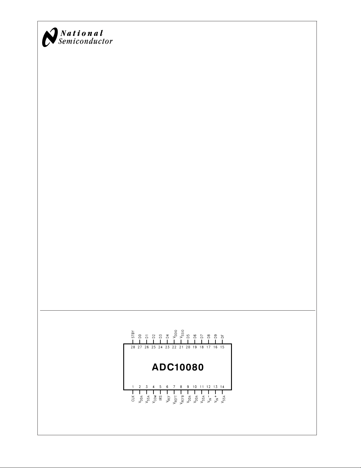
Connection Diagram
20048501
© 2004 National Semiconductor Corporation DS200485 www.national.com
Page 2
Ordering Information
ADC10080
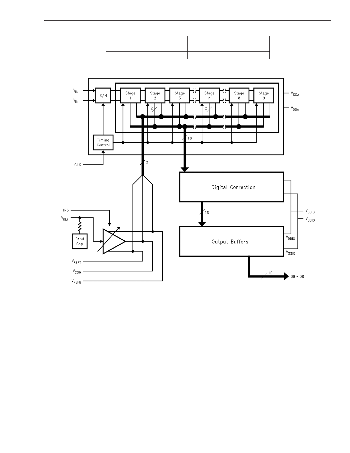
Block Diagram
Industrial (−40˚C ≤ TA≤ +85˚C) NS Package
ADC10080CIMT 28 Pin TSSOP
ADC10080CIMTX 28 Pin TSSOP Tape & Reel
www.national.com 2
20048502
Page 3
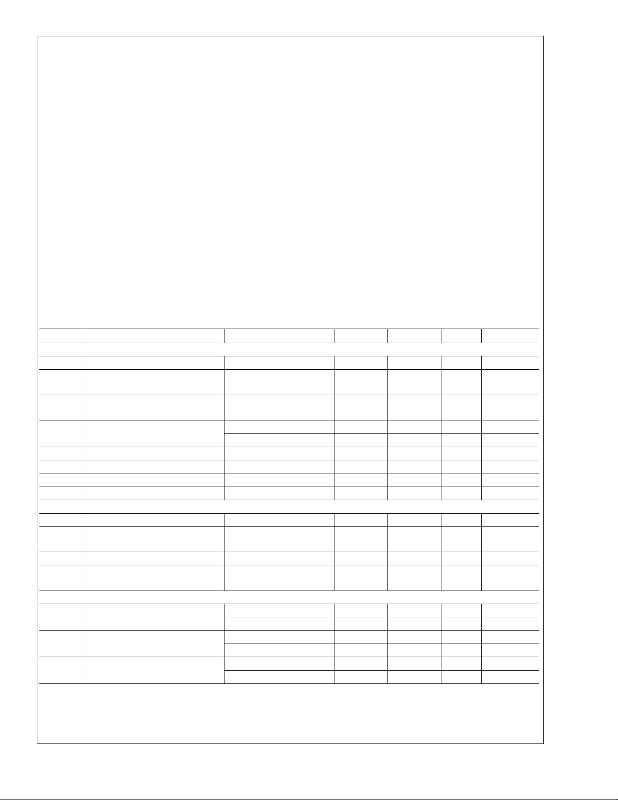
Pin Descriptions and Equivalent Circuits
Pin No. Symbol Equivalent Circuit Description
ANALOG I/O
Inverting analog input signal. With a 1.2V reference the
12 V
−
IN
full-scale input signal level is 1.0 V
(pin 4) for single-ended operation.
V
COM
. This pin may be tied to
P-P
ADC10080
13 V
6V
7V
4V
8V
IN
REF
REFT
COM
REFB
+
Non-inverting analog input signal. With a 1.2V reference the
full-scale input signal level is 1.0 V
Reference input. This pin should be bypassed to V
0.1 µF monolithic capacitor. V
.
P-P
is 1.20V nominal. This pin
REF
SSA
with a
may be driven by a 1.20V external reference if desired. Do
not load this pin.
V
REFT
and V
are high impedance reference bypass pins
REFB
only. Connect a 0.1 µF capacitor from each of these pins to
. These pins should not be loaded. V
V
SSA
bypassed with a 0.1 µF capacitor to V
to set the input common voltage V
CM
SSA.VCOM
.
should also be
COM
may be used
DIGITAL I/O
1 CLK
15 DF
28 STBY
5
IRS (Input Range
Select)
Digital clock input. The range of frequencies for this input is
20 MHz to 80 MHz. The input is sampled on the rising edge
of this input.
DF = “1” Two’s Complement
DF = “0” Offset Binary
This is the standby pin. When high, this pin sets the converter
into standby mode. When this pin is low, the converter is in
active mode.
IRS=“V
IRS=“V
DDA
SSA
” 2.0 V
” 1.5 V
IRS = “Floating” 1.0 V
If using both V
IN
input range
P-P
input range
P-P
input range
P-P
+ and VIN- pins, (or differential mode), then
the peak-to-peak voltage refers to the differential voltage
+-VIN-).
(V
IN
www.national.com3
Page 4
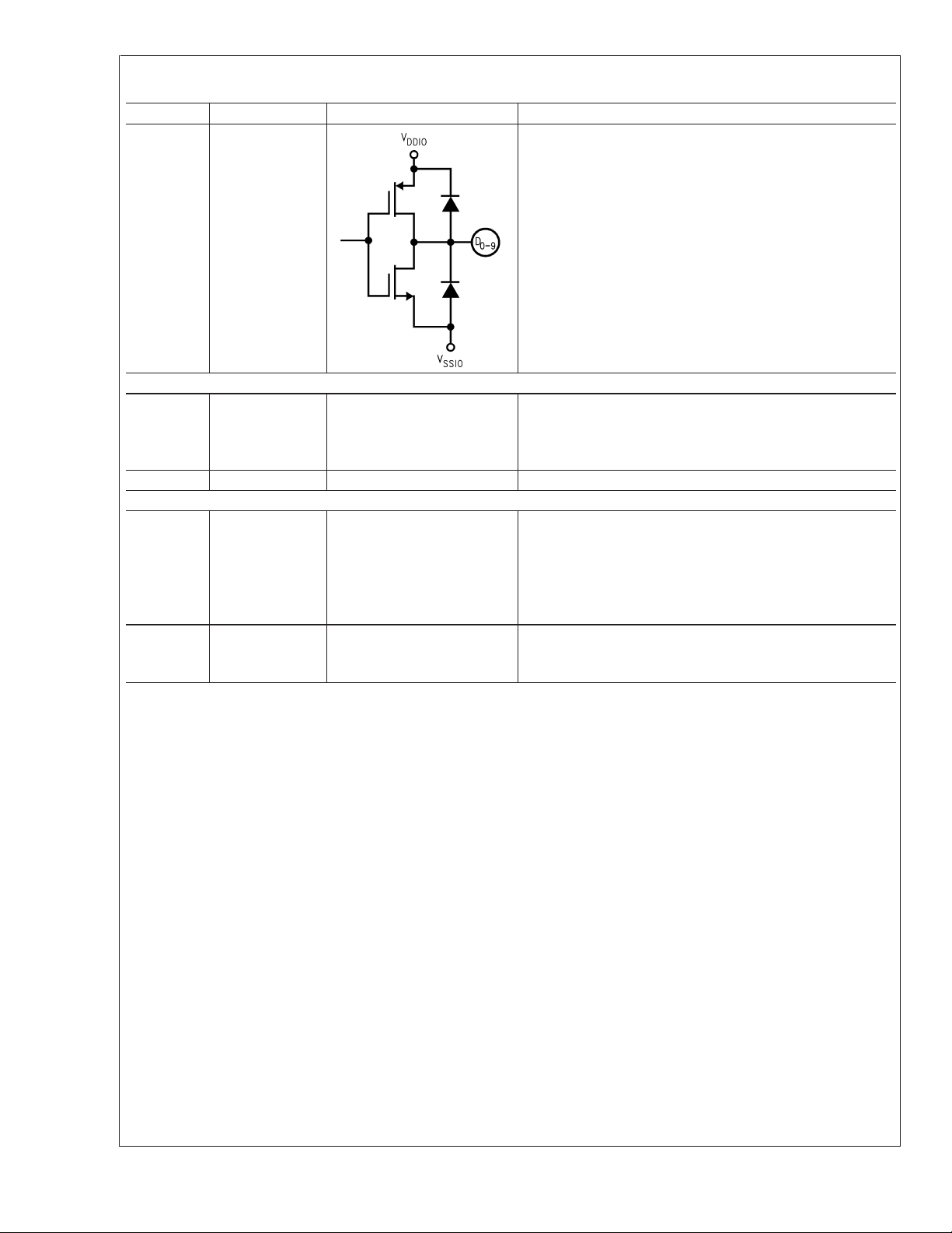
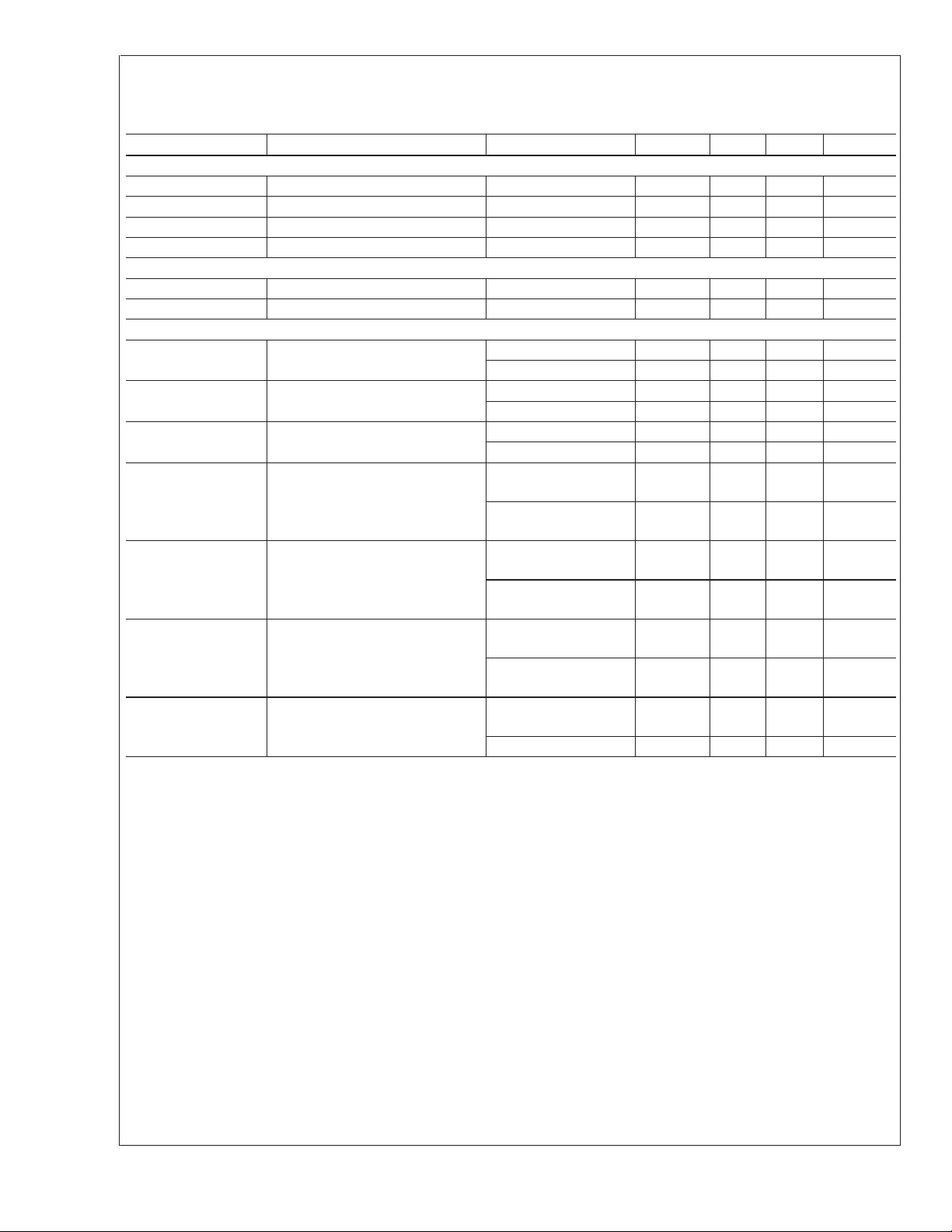
Pin Descriptions and Equivalent Circuits (Continued)
Pin No. Symbol Equivalent Circuit Description
ADC10080
16–20,
23–27
ANALOG POWER
2, 9, 10 V
3, 11, 14 V
DIGITAL POWER
22 V
21 V
D0–D9
DDA
SSA
DDIO
SSIO
Digital output data. D0 is the LSB and D9 is the MSB of the
binary output word.
Positive analog supply pins. These pins should be connected
to a quiet 3.0V source and bypassed to analog ground with a
0.1 µF monolithic capacitor located within 1 cm of these pins.
A 4.7 µF capacitor should also be used in parallel.
Ground return for the analog supply.
Positive digital supply pins for the ADC10080’s output drivers.
This pin should be bypassed to digital ground with a 0.1 µF
monolithic capacitor located within 1 cm of this pin. A 4.7 µF
capacitor should also be used in parallel. The voltage on this
pin should never exceed the voltage on V
by more than
DDA
300 mV.
The ground return for the digital supply for the output drivers.
This pin should be connected to the digital ground, but not
near the analog ground.
www.national.com 4
Page 5
ADC10080
Absolute Maximum Ratings (Notes 1,
2)
If Military/Aerospace specified devices are required,
please contact the National Semiconductor Sales Office/
Distributors for availability and specifications.
V
DDIO
DDA
+0.3V
±
25 mA
±
50 mA
3.9V
or
V
DDA,VDDIO
Voltage on Any Pin to GND −0.3V to V
Input Current on Any Pin
Package Input Current (Note 3)
Package Dissipation at T = 25˚C See (Note 4)
Operating Ratings
Operating Temperature Range −40˚C ≤ TA≤ +85˚C
V
(Supply Voltage) +2.7V to +3.6V
DDA
V
(Output Driver Supply
DDIO
Voltage) +2.5V to V
V
REF
|V
SSA–VSSIO
NOTE: Absolute maximum ratings are limiting values, to be applied individually, and beyond which the serviceability of the circuit may be impaired.
Functional operability under any of these conditions is not necessarily implied. Exposure to maximum ratings for extended periods may affect device
reliability.
| ≤ 100 mV
1.20V
ESD Susceptibility
Human Body Model (Note 5) 2500V
Machine Model (Note 5) 250V
Soldering Temperature
Infrared, 10 sec. (Note 6) 235˚C
Storage Temperature −65˚C to +150˚C
Converter Electrical Characteristics
Unless otherwise specified, the following specifications apply for V
=2V
V
IN
apply for T
, STBY = 0V, V
P-P
A=TMIN
to T
= 1.20V, (External Supply) f
REF
: all other limits TA= 25˚C.
MAX
SSA=VSSIO
= 80 MHz, 50% Duty Cycle, CL= 10 pF/pin. Boldface limits
CLK
Symbol Parameter Conditions Min Typ Max Units
STATIC CONVERTER CHARACTERISTICS
No Missing Codes Guaranteed 10 Bits
F
= 500 kHz, 0 dB Full
INL Integral Non-Linearity (Note 11)
DNL Differential Non-Linearity
GE Gain Error
OE Offset Error (V
+=VIN−) −1.4 0.11 1.7 %FS
IN
IN
Scale
F
= 500 kHz, 0 dB Full
IN
Scale
Positive Error −1.6 +0.5% +2.0 %FS
Negative Error −1.6 −0.07% +2.0 %FS
Under Range Output Code 0
Over Range Output Code 1023
FPBW Full Power Bandwidth 400 MHz
REFERENCE AND INPUT CHARACTERISTICS
V
V
V
CM
COM
REF
V
REFTC
Common Mode Input Voltage 0.5 1.5 V
Output Voltage for use as an input
common mode voltage (Note 16)
Reference Voltage 1.2 V
Reference Voltage Temperature
Coefficient
POWER SUPPLY CHARACTERISTICS
I
VDDA
I
VDDIO
Analog Supply Current
Digital Supply Current
PWR Power Consumption
STBY = 1 5 6.3 mA
STBY 0 25 32 mA
STBY=1,f
STBY 0, f
=0Hz 0 mA
IN
=0Hz 1.2 1.4 mA
IN
STBY = 1 15 18.9 mW
STBY = 0 78.6 100.2 mW
= 0V, V
−1.4
−0.9
DDA
= +3.0V, V
±
0.5 +1.6 LSB
±
0.25 +1.0 LSB
DDIO
= +2.5V,
1.45
±
80 ppm/˚C
V
DDA
www.national.com5
Page 6
DC and Logic Electrical Characteristics Unless otherwise specified, the following specifications
apply for V
= 80 MHz, 50% Duty Cycle, CL= 10 pF/pin. Boldface limits apply for TA=T
f
CLK
ADC10080
SSA=VSSIO
= 0V, V
Symbol Parameter Conditions Min Typ Max Units
CLK, DF, STBY, SENSE
Logical “1” Input Voltage 2 V
Logical “0” Input Voltage 0.8 V
Logical “1” Input Current +10 µA
Logical “0” Input Current −10 µA
D0–D9 OUTPUT CHARACTERISTICS
Logical “1” Output Voltage I
Logical “0” Output Voltage I
DYNAMIC CONVERTER CHARACTERISTICS
ENOB Effective Number of Bits
SNR Signal-to-Noise Ratio
SINAD Signal-to-Noise Ratio + Distortion
2nd HD 2nd Harmonic
3rd HD 3rd Harmonic
THD
SFDR
Total Harmonic Distortion (First 6
Harmonics)
Spurious Free Dynamic Range
(Excluding 2nd and 3rd Harmonic)
DDA
= +3.0V, V
= +2.5V, VIN=2V
DDIO
, STBY = 0V, V
P-P
MIN
= −0.5 mA V
OUT
= 1.6 mA 0.4 V
OUT
f
= 10.0 MHz 9.3, 9.1 9.5 Bits
IN
f
= 39 MHz 9.3, 8.9 9.5 Bits
IN
f
= 10.0 MHz 58.5, 57.7 59.5 dB
IN
f
= 39 MHz 58.0, 57.0 59.2 dB
IN
f
= 10.0 MHz 58.0, 56.3 59.2 dB
IN
f
= 39 MHz 57.6, 55.6 59.0 dB
IN
f
= 10.0 MHz −74.1,
IN
fIN= 39 MHz −69.5,
= 10.0 MHz −65,
f
IN
fIN= 39 MHz −64.7,
= 10.0 MHz −65,
f
IN
= 39 MHz −64.7,
f
IN
fIN= 10.0 MHz −70.8,
= 39 MHz −72, −68 −78.8 dBc
f
IN
= 1.20V, (Externally Supplied)
REF
to T
DDIO
: all other limits TA= 25˚C
MAX
−0.2 V
−68.7
−62.7
−58.6
−57.6
−58.6
−57.6
−68.2
−87.0 dBc
−82 dBc
−72.3 dBc
−74.5 dBc
−72.3 dB
−74.5 dB
−78.7 dBc
www.national.com 6
Page 7

AC Electrical Characteristics
Unless otherwise specified, the following specifications apply for V
, STBY = 0V, V
2V
P-P
ply for T
A=TMIN
= 1.20V, (Externally Supplied) f
REF
to T
: all other limits TA= 25˚C
MAX
CLK
SSA=VSSIO
= 80 MHz, 50% Duty Cycle, CL= 10 pF/pin. Boldface limits ap-
Symbol Parameter Conditions Min
CLK, DF, STBY, SENSE
1 Maximum Clock Frequency 80 MHz (min)
f
CLK
f
2 Minimum Clock Frequency 20 MHz
CLK
t
CH
t
CL
t
CONV
t
OD
t
AD
t
AJ
Clock High Time 6.25 ns
Clock Low Time 6.25 ns
Conversion Latency 6 Cycles
Data Output Delay after a Rising
T = 25˚C 2 3.5 5 ns
Clock Edge
Aperture Delay 1 ns
Aperture Jitter 2 ps (RMS)
Over Range Recovery Time
Differential V
±
3V to 0V to get
step from
IN
accurate conversion
t
STBY
Note 1: Absolute Maximum Ratings indicate limits beyond which damage to the device may occur. Operating Ratings indicate conditions for which the device is
functional, but do not guarantee specific performance limits. For guaranteed specifications and test conditions, see the Electrical Characteristics. The guaranteed
specifications apply only for the test conditions listed. Some performance characteristics may degrade when the device is not operated under the listed test
conditions.
Note 2: All voltages are measured with respect to GND = V
Note 3: When the voltage at any pin exceeds the power supplies (V
The 50 mA maximum package input current rating limits the number of pins that can safely exceed the power supplies with an input current of 25 mA to two.
Note 4: The absolute maximum junction temperature (T
junction-to-ambient thermal resistance (θ
TSSOP, θ
this device under normal operation will typically be about 78.6 mW. The values for maximum power dissipation listed above will be reached only when the ADC10080
is operated in a severe fault condition.
Note 5: Human body model is 100 pF capacitor discharged through a 1.5 kΩ resistor. Machine model is 220 pF discharged through 0Ω.
Note 6: The 235˚C reflow temperature refers to infrared reflow. For Vapor Phase Reflow (VPR) the following conditions apply: Maintain the temperature at the top
of the package body above 183˚C for a minimum of 60 seconds. The temperature measured on the package body must not exceed 220˚C. Only one excursion above
183˚C is allowed per reflow cycle. The analog inputs are protected as shown below. Input voltage magnitude up to 500 mV beyond the supply rails will not damage
this device. However, input errors will be generated if the input goes above V
Standby Mode Exit Cycle 20 Cycles
SSA=VSSIO
max) for this device is 150˚C. The maximum allowable power dissipation is dictated by TJmax, the
), and the ambient temperature (TA), and can be calculated using the formula PDMAX=(TJmax − TA)/θJA. In the 28-pin
is 96˚C/W, so PDMAX = 1,302 mW at 25˚C and 677 mW at the maximum operating ambient temperature of 85˚C. Note that the power dissipation of
JA
JA
J
= 0V, unless otherwise specified.
<
V
IN
SSA
DDA
or V
or V
IN
>
V
DDA,VDDIO
DDIO
= 0V, V
(Note 11)
and below V
DDA
= +3.0V, V
Typ
(Note
11)
= +2.5V, VIN=
DDIO
Max
(Note
11)
Units
16ns
1 Clock Cycle
or VDR), the current at that pin should be limited to 25 mA.
or V
SSIO
.
SSA
ADC10080
20048507
Note 7: To guarantee accuracy, it is required that |V
Note 8: With the test condition for 2 V
Note 9: Typical figures are at T
Level).
Note 10: Integral Non Linearity is defined as the deviation of the analog value, expressed in LSBs, from the straight line that passes through positive and negative
full-scale.
Note 11: Timing specifications are tested at TTL logic levels, V
Note 12: Optimum dynamic performance will be obtained by keeping the reference input in the +1.2V.
Note 13: I
V
DR
supply voltage, C
Note 14: Power consumption includes output driver power. (f
Note 15: The input bandwidth is limited using a 10 pF capacitor between V
Note 16: V
is the current consumed by the switching of the output drivers and is primarily determined by load capacitance on the output pins, the supply voltage,
DR
, and the rate at which the outputs are switching (which is signal dependent). IDR=VDRx(C0xf0+C1xf1+C2+f2+....C11xf11) where VDRis the output driver
is the total load capacitance on the output pin, and fnis the average frequency at which the pin is toggling.
n
is typical value, measured at room temperature. It is not guaranteed by test.
COM
P-P
= 25˚C and represent most likely parametric norms. Test limits are guaranteed to National’s AOQL (Average Outgoing Quality
A=TJ
DDA–VDDIO
differential input, the 10-bit LSB is 1.95 mV.
| ≤ 100 mV and separate bypass capacitors are used at each power supply pin.
= 0.4V for a falling edge, and VIH= 2.4V for a rising edge.
IL
= 0 MHz).
IN
IN
−
and V
+
.
IN
www.national.com7
Page 8

Specification Definitions
APERTURE DELAY is the time after the rising edge of the
clock to when the input signal is acquired or held for conver-
ADC10080
sion.
APERTURE JITTER (APERTURE UNCERTAINTY) is the
variation in aperture delay from sample to sample. Aperture
jitter manifests itself as noise in the output.
COMMON MODE VOLTAGE (V
present at both signal inputs to the ADC.
CONVERSION LATENCY See PIPELINE DELAY.
DIFFERENTIAL NON-LINEARITY (DNL) is the measure of
the maximum deviation from the ideal step size of 1 LSB.
DUTY CYCLE is the ratio of the time that a repetitive digital
waveform is high to the total time of one period. The specification here refers to the ADC clock input signal.
EFFECTIVE NUMBER OF BITS (ENOB, or EFFECTIVE
BITS) is another method of specifying Signal-to-Noise and
Distortion or SINAD. ENOB is defined as (SINAD - 1.76) /
6.02 and states that the converter is equivalent to a perfect
ADC of this (ENOB) number of bits.
FULL POWER BANDWIDTH is a measure of the frequency
at which the reconstructed output fundamental drops 3 dB
below its low frequency value for a full scale input.
GAIN ERROR is the deviation from the ideal slope of the
transfer function. It can be calculated as:
Gain Error = Positive Full-Scale Error − Negative Full-
Scale Error
INTEGRAL NON LINEARITY (INL) is a measure of the
deviation of each individual code from a line drawn from
negative full scale (
1
⁄2LSB below the first code transition)
through positive full scale (
transition). The deviation of any given code from this straight
line is measured from the center of that code value.
MISSING CODES are those output codes that will never
appear at the ADC outputs. The ADC10080 is guaranteed
not to have any missing codes.
NEGATIVE FULL SCALE ERROR is the difference between
+
−
the input voltage (V
−V
IN
IN
negative full scale to the first code and its ideal value of
0.5 LSB.
OFFSET ERROR is the input voltage that will cause a tran-
sition from a code of 01 1111 1111 to a code of 10 0000 0000.
OUTPUT DELAY is the time delay after the rising edge of
the clock before the data update is presented at the output
pins.
) is the d.c. potential
CM
1
⁄2LSB above the last code
) just causing a transition from
PIPELINE DELAY (LATENCY) is the number of clock cycles
between initiation of conversion and when that data is presented to the output driver stage. Data for any given sample
is available at the output pins the Pipeline Delay plus the
Output Delay after the sample is taken. New data is available
at every clock cycle, but the data lags the conversion by the
pipeline delay.
POSITIVE FULL SCALE ERROR is the difference between
the actual last code transition and its ideal value of 1
1
⁄2LSB
below positive full scale.
SIGNAL TO NOISE RATIO (SNR) is the ratio, expressed in
dB, of the rms value of the input signal to the rms value of the
sum of all other spectral components below one-half the
sampling frequency, not including harmonics or dc.
SIGNAL TO NOISE PLUS DISTORTION (S/N+D or SINAD)
Is the ratio, expressed in dB, of the rms value of the input
signal to the rms value of all of the other spectral components below half the clock frequency, including harmonics
but excluding dc.
SPURIOUS FREE DYNAMIC RANGE (SFDR) is the difference, expressed in dB, between the rms values of the input
signal and the peak spurious signal, where a spurious signal
is any signal present in the output spectrum that is not
present at the input.
TOTAL HARMONIC DISTORTION (THD) is the ratio, expressed in dBc, of the rms total of the first six harmonic
levels at the output to the level of the fundamental at the
output. THD is calculated as:
where f1is the RMS power of the fundamental (output)
frequency and f
through f6are the RMS power in the first 6
2
harmonic frequencies.
Second Harmonic Distortion (2nd Harm) is the difference
expressed in dB, between the RMS power in the input
frequency at the output and the power in its 2nd harmonic
level at the output.
Third Harmonic Distortion (3rd Harm) is the difference,
expressed in dB, between the RMS power in the input
frequency at the output and the power in its 3rd harmonic
level at the output.
www.national.com 8
Page 9

Timing Diagram
Transfer Characteristics
ADC10080
20048509
FIGURE 1. Clock and Data Timing Diagram
FIGURE 2. Input vs. Output Transfer Characteristic
20048510
www.national.com9
Page 10

Typical Performance Characteristics Unless otherwise specified, the following specifications apply:
V
SSA=VSSIO
, 39 MHz, 50% Duty Cycle.
f
IN
ADC10080
= 0V, V
DNL vs. Clock Duty Cycle (DC input) DNL vs. Temperature
DDA
= +3.0V, V
= +2.5V, VIN=2V
DDIO
, STBY = 0V, V
P-P
= 1.2V, (External Supply) f
REF
DNL DNL vs. f
20048512 20048515
CLK
CLK
= 80 MHz,
20048513
INL INL vs. f
20048514 20048517
www.national.com 10
20048516
CLK
Page 11

Typical Performance Characteristics Unless otherwise specified, the following specifications apply:
=V
V
SSA
, 39 MHz, 50% Duty Cycle. (Continued)
f
IN
SSIO
= 0V, V
DDA
= +3.0V, V
= +2.5V, VIN=2V
DDIO
, STBY = 0V, V
P-P
= 1.2V, (External Supply) f
REF
= 80 MHz,
CLK
ADC10080
INL vs. Clock Duty Cycle SNR vs. V
20048518
SNR vs. V
DDA
SNR vs. f
DDIO
20048519
CLK
20048520
INL vs. Temperature SNR vs. Clock Duty Cycle
20048522
20048521
20048523
www.national.com11
Page 12

Typical Performance Characteristics Unless otherwise specified, the following specifications apply:
=V
V
SSA
, 39 MHz, 50% Duty Cycle. (Continued)
f
IN
ADC10080
SSIO
= 0V, V
= +3.0V, V
DDA
= +2.5V, VIN=2V
DDIO
, STBY = 0V, V
P-P
= 1.2V, (External Supply) f
REF
SNR vs. Temperature THD vs. V
20048524 20048525
DDA
= 80 MHz,
CLK
THD vs. V
DDIO
20048526
THD vs. f
SNR vs. IRS THD vs. IRS
CLK
20048527
20048528
www.national.com 12
20048529
Page 13

Typical Performance Characteristics Unless otherwise specified, the following specifications apply:
=V
V
SSA
, 39 MHz, 50% Duty Cycle. (Continued)
f
IN
SSIO
= 0V, V
DDA
= +3.0V, V
= +2.5V, VIN=2V
DDIO
, STBY = 0V, V
P-P
= 1.2V, (External Supply) f
REF
= 80 MHz,
CLK
ADC10080
SINAD vs. V
DDA
20048530
SINAD vs. V
DDIO
THD vs. Clock Duty Cycle SINAD vs. Clock Duty Cycle
20048531
20048532 20048533
THD vs. Temperature SINAD vs. Temperature
20048534 20048535
www.national.com13
Page 14

Typical Performance Characteristics Unless otherwise specified, the following specifications apply:
=V
V
SSA
, 39 MHz, 50% Duty Cycle. (Continued)
f
IN
ADC10080
SSIO
= 0V, V
= +3.0V, V
DDA
SINAD vs. f
= +2.5V, VIN=2V
DDIO
CLK
, STBY = 0V, V
P-P
= 1.2V, (External Supply) f
REF
SFDR vs. V
DDIO
= 80 MHz,
CLK
20048536
SINAD vs. IRS SFDR vs. f
20048538
SFDR vs. V
DDA
SFDR vs. IRS
20048537
CLK
20048539
20048540
www.national.com 14
20048541
Page 15

Typical Performance Characteristics Unless otherwise specified, the following specifications apply:
=V
V
SSA
, 39 MHz, 50% Duty Cycle. (Continued)
f
IN
SSIO
= 0V, V
DDA
= +3.0V, V
= +2.5V, VIN=2V
DDIO
, STBY = 0V, V
P-P
= 1.2V, (External Supply) f
REF
= 80 MHz,
CLK
ADC10080
SFDR vs. Clock Duty Cycle Spectral Response
20048542
@
10 MHz Input
SFDR vs. Temperature Spectral Response@39 MHz Input
20048543
Power Consumption vs. f
20048544 20048545
CLK
20048546
www.national.com15
Page 16

Functional Description
The ADC10080 uses a pipeline architecture and has error
correction circuitry to help ensure maximum performance.
ADC10080
Differential analog input signals are digitized to 10 bits. In
differential mode each analog input signal should have a
peak-to-peak voltage equal to 1.0V, 0.75V or 0.5V, depending on the state of the IRS pin (pin 5), and be centered
around V
single ended operation is desired, V
V
COM
applied to V
range of V
and be 180˚ out of phase with each other. If
CM
- may be tied to the
IN
pin (pin 4). A single ended input signal may then be
+, and should have an average value in the
IN
. The signal amplitude should be 2.0V, 1.5V or
CM
1.0V peak-to-peak, depending on the state or the IRS pin
(pin 5).
Applications Information
1.0 ANALOG INPUTS
The ADC10080 has two analog signal inputs, V
These two pins form a differential input pair. There is one
common mode pin V
mon mode input voltage.
1.1 REFERENCE PINS
The ADC10080 is designed to operate with a 1.2V reference,
but performs well with reference voltages in the range of
0.8V to 2.0V. Lower reference voltages will decrease the
signal-to-noise ratio (SNR) of the ADC10080. It is very important that all grounds associated with the reference voltage and the input signal make connection to the analog
ground plane at a single point to minimize the effects of
noise currents in the ground path. The three Reference
Bypass Pins V
REF,VREFT
bypass purposes only. These pins should each be bypassed
to ground with a 0.1 µF capacitor. DO NOT LOAD these pins.
1.2 V
COM
PIN
This pin supplies a voltage for possible use to set the common mode input voltage. This pin may also be connected to
-, so that VIN+ may be used as a single ended input. This
V
IN
pin should be byassed with at least a 0.1 uF capacitor.
1.3 SIGNAL INPUTS
The signal inputs are V
tude is defined as V
cally in Figure 3:
that may be used to set the com-
COM
and V
+ and VIN−. The input signal ampli-
IN
+−VIN− and is represented schemati-
IN
, are made available for
REFB
+ and VIN−.
IN
20048548
FIGURE 4. Input Voltage Waveform for a 2V
P-P
Single
Ended Input
The internal switching action at the analog inputs causes
energy to be output from the input pins. As the driving source
tries to compensate for this, it adds noise to the signal. To
prevent this, use 18Ω series resistors at each of the signal
inputs with a 25 pF capacitor across the inputs, as can be
seen in Figure 5. These components should be placed close
to the ADC because the input pins of the ADC is the most
sensitive part of the system and this is the last opportunity to
filter the input. The two 18Ω resistors and the 25 pF capacitor form a low-pass filter with a -3 dB frequency of 177 MHz
.
1.4 CLK PIN
The CLK signal controls the timing of the sampling process.
Drive the clock input with a stable, low jitter clock signal in
the range of 20 MHz to 80 MHz with rise and fall times of less
than 2 ns. The trace carrying the clock signal should be as
short as possible and should not cross any other signal line,
analog or digital, not even at 90˚. The CLK signal also drives
an internal state machine. If the CLK is interrupted, or its
frequency is too low, the charge on internal capacitors can
dissipate to the point where the accuracy of the output data
will degrade. This is what limits the lowest sample rate to
20 MSPS. The duty cycle of the clock signal can affect the
performance of any A/D Converter. Because achieving a
precise duty cycle is difficult, the ADC10080 is designed to
maintain performance over a range of duty cycles. While it is
specified and performance is guaranteed with a 50% clock
duty cycle, performance is typically maintained over a clock
duty cycle range of 40% to 60%.
1.5 STBY PIN
The STBY pin, when high, holds the ADC10080 in a powerdown mode to conserve power when the converter is not
being used. The power consumption in this state is 15 mW.
The output data pins are undefined in this mode. Power
consumption during power-down is not affected by the clock
frequency, or by whether there is a clock signal present. The
data in the pipeline is corrupted while in the power down.
20048547
FIGURE 3. Input Voltage Waveforms for a 2V
P-P
Differential Input
A single ended input signal is shown in Figure 4.
www.national.com 16
1.6 DF PIN
The DF pin, when high, forces the ADC10080 to output the
2’s complement data format. When DF is tied low, the output
format is offset binary.
1.7 IRS PIN
The IRS (Input Range Select) pin defines the input signal
amplitude that will produce a full scale output. The table
below describes the function of the IRS pin.
Page 17

Applications Information (Continued)
TABLE 1. IRS Pin Functions
IRS Pin Full-Scale Input
V
DDA
V
SSA
Floating 1.0V
1.8 OUTPUT PINS
The ADC10080 has 10 TTL/CMOS compatible Data Output
pins. The offset binary data is present at these outputs while
the DF and STBY pins are low. While the t
information about output timing, a simple way to capture a
valid output is to latch the data on the rising edge of the
conversion clock. Be very careful when driving a high capacitance bus. The more capacitance the output drivers
must charge for each conversion, the more instantaneous
digital current flows through V
DDIO
2.0V
1.5V
and V
P-P
P-P
P-P
OD
SSIO
time provides
. These large
charging current spikes can cause on-chip ground noise and
couple into the analog circuitry, degrading dynamic performance. Adequate bypassing, limiting output capacitance and
careful attention to the ground plane will reduce this problem. Additionally, bus capacitance beyond the specified
10 pF/pin will cause t
to increase, making it difficult to
OD
properly latch the ADC output data. The result could be an
apparent reduction in dynamic performance. To minimize
noise due to output switching, minimize the load currents at
the digital outputs. This can be done by connecting buffers
between the ADC outputs and any other circuitry. Only one
driven input should beADC pins, will isolate the outputs from
trace and other circuit capacitances and limit the output
currents, which could otherwise result in performance degradation.
1.9 APPLICATION SCHEMATICS
The following figures show simple examples of using the
ADC10080. Figure 5 shows a typical differentially driven
input. Figure 6 shows a single ended application circuit.
ADC10080
FIGURE 5. A Simple Application Using a Differential Driving Source
20048549
www.national.com17
Page 18

Applications Information (Continued)
ADC10080
FIGURE 6. A Simple Application Using a Single Ended Driving Source
20048550
www.national.com 18
Page 19

Physical Dimensions inches (millimeters) unless otherwise noted
ADC10080 10-Bit 80 MSPS 3V, 78.6 mW A/D Converter
28-Lead TSSOP Package
Ordering Number ADC10080CIMT
NS Package Number MTC28
National does not assume any responsibility for use of any circuitry described, no circuit patent licenses are implied and National reserves
the right at any time without notice to change said circuitry and specifications.
For the most current product information visit us at www.national.com.
LIFE SUPPORT POLICY
NATIONAL’S PRODUCTS ARE NOT AUTHORIZED FOR USE AS CRITICAL COMPONENTS IN LIFE SUPPORT DEVICES OR SYSTEMS
WITHOUT THE EXPRESS WRITTEN APPROVAL OF THE PRESIDENT AND GENERAL COUNSEL OF NATIONAL SEMICONDUCTOR
CORPORATION. As used herein:
1. Life support devices or systems are devices or systems
which, (a) are intended for surgical implant into the body, or
(b) support or sustain life, and whose failure to perform when
properly used in accordance with instructions for use
2. A critical component is any component of a life support
device or system whose failure to perform can be reasonably
expected to cause the failure of the life support device or
system, or to affect its safety or effectiveness.
provided in the labeling, can be reasonably expected to result
in a significant injury to the user.
BANNED SUBSTANCE COMPLIANCE
National Semiconductor certifies that the products and packing materials meet the provisions of the Customer Products Stewardship
Specification (CSP-9-111C2) and the Banned Substances and Materials of Interest Specification (CSP-9-111S2) and contain no ‘‘Banned
Substances’’ as defined in CSP-9-111S2.
National Semiconductor
Americas Customer
Support Center
Email: new.feedback@nsc.com
Tel: 1-800-272-9959
www.national.com
National Semiconductor
Europe Customer Support Center
Fax: +49 (0) 180-530 85 86
Email: europe.support@nsc.com
Deutsch Tel: +49 (0) 69 9508 6208
English Tel: +44 (0) 870 24 0 2171
Français Tel: +33 (0) 1 41 91 8790
National Semiconductor
Asia Pacific Customer
Support Center
Email: ap.support@nsc.com
National Semiconductor
Japan Customer Support Center
Fax: 81-3-5639-7507
Email: jpn.feedback@nsc.com
Tel: 81-3-5639-7560
 Loading...