

Page 1
December 1994
ADC10061/ADC10062/ADC10064 10-Bit 600 ns
A/D Converter with Input Multiplexer and Sample/Hold
ADC10061/ADC10062/ADC10064 10-Bit 600 ns A/D Converter
with Input Multiplexer and Sample/Hold
General Description
Using an innovative, patented multistep* conversion technique, the 10-bit ADC10061, ADC10062, and ADC10064
CMOS analog-to-digital converters offer sub-microsecond
conversion times yet dissipate a maximum of only 235 mW.
The ADC10061, ADC10062, and ADC10064 perform a
10-bit conversion in two lower-resolution ‘‘flashes’’, thus
yielding a fast A/D without the cost, power dissipation, and
other problems associated with true flash approaches. The
ADC10061 is pin-compatible with the ADC1061 but much
faster, thus providing a convenient upgrade path for the
ADC1061.
The analog input voltage to the ADC10061, ADC10062, and
ADC10064 is sampled and held by an internal sampling circuit. Input signals at frequencies from dc to over 200 kHz
can therefore be digitized accurately without the need for an
external sample-and-hold circuit.
The ADC10062 and ADC10064 include a ‘‘speed-up’’ pin.
Connecting an external resistor between this pin and ground
reduces the typical conversion time to as little as 350 ns
with only a small increase in linearity error.
For ease of interface to microprocessors, the ADC10061,
ADC10062, and ADC10064 have been designed to appear
as a memory location or I/O port without the need for external interface logic.
Ordering Information
ADC10061
s
Industrial (b40§CsT
ADC10061BIN, ADC10061CIN N20A Molded DIP
ADC10061BIWM, ADC10061CIWM M20B Small Outline
a
85§C) Package
A
Features
Y
Built-in sample-and-hold
Y
Singlea5V supply
Y
1, 2, or 4-input multiplexer options
Y
No external clock required
Y
Speed adjust pin for faster conversions (ADC10062 and
ADC10064). See ADC10662/4 for high speed guaranteed performance.
Key Specifications
Y
Conversion time to 10 bits 600 ns typical,
900 ns max over temperature
Y
Sampling Rate 800 kHz
Y
Low power dissipation 235 mW (max)
Y
Total unadjusted error
Y
No missing codes over temperature
g
1.0 LSB (max)
Applications
Y
Digital signal processor front ends
Y
Instrumentation
Y
Disk drives
Y
Mobile telecommunications
ADC10064
s
Industrial (b40§CsT
ADC10064BIN, ADC10064CIN N28B Molded DIP
ADC10064BIWM, ADC10064CIWM M28B Small Outline
a
85§C) Package
A
s
Military (b55§CsT
a
125§C) Package
A
ADC10061CMJ/883 J20A Cerdip
Military (b55§CsT
ADC10064CMJ/883 J28A Cerdip
s
a
125§C) Package
A
ADC10062
s
Industrial (b40§CsT
a
85§C) Package
A
ADC10062BIN, ADC10062CIN N24A Molded DIP
ADC10062BIWM, ADC10062CIWM M24B Small Outline
s
Military (b55§CsT
a
125§C) Package
A
ADC10062CMJ/883 J24A Cerdip
*U.S. Patent Number 4918449
TRI-STATEÉis a registered trademark of National Semiconductor Corporation.
C
1995 National Semiconductor Corporation RRD-B30M75/Printed in U. S. A.
TL/H/11020
Page 2
Absolute Maximum Ratings (Notes 1, 2)
If Military/Aerospace specified devices are required,
please contact the National Semiconductor Sales
Office/Distributors for availability and specifications.
Supply Voltage (V
Voltage at Any Input or Output
Input Current at Any Pin (Note 3) 5 mA
Package Input Current (Note 3) 20 mA
Power Dissipation (Note 4) 875 mW
ESD Susceptability (Note 5) 2000V
Soldering Information (Note 6)
N Package (10 Sec) 260
J Package (10 Sec) 300
SO Package:
Vapor Phase (60 Sec) 215
Infrared (15 Sec) 220
Storage Temperature Range
Junction Temperature 150§C
a
e
AV
CC
e
DVCC)
b
0.3V toa6V
b
0.3V to V
b
65§Ctoa150§C
a
a
0.3V
Operating Ratings (Notes 1, 2)
s
s
T
Temperature Range T
ADC10061BIN, ADC10061BIWM,
MIN
ADC10061CIN, ADC10061CIWM,
ADC10062BIN, ADC10062BIWM,
ADC10062CIN, ADC10062CIWM,
ADC10064BIN, ADC10064BIWM,
ADC10064CIN,
ADC10064CIWM
ADC10061CMJ/883, ADC10062CMJ/883,
ADC10064CMJ/883
b
40§CsT
b
55§CsT
Supply Voltage Range 4.5V to 5.5V
C
§
C
§
C
§
C
§
T
A
MAX
s
a
85§C
A
s
a
125§C
A
Converter Characteristics
The following specifications apply for V
unless otherwise specified. Boldface limits apply for T
a
ea
5V, V
REF(a)
A
e
ea
T
J
e
5V, V
T
Min
Symbol Parameter Conditions
Resolution 10 Bits
Integral Linearity Error BIN, BIWM Suffixes
CIN, CIWM, CMJ Suffixes
e
R
18 kX
SA
Offset Error
Full-Scale Error
Total Unadjusted Error BIN, BIWM Suffixes
CIN, CIWM, CMJ Suffixes
All Suffixes, R
e
SA
Missing Codes 0 (max)
a
Power Supply Sensitivity V
THD Total Harmonic Distortion f
SNR Signal-to-Noise Ratio f
Effective Number of Bits f
R
REF
R
REF
V
REF(a)VREF(a)
V
REF(b)VREF(b)
V
REF(a)VREF(a)
V
REF(b)VREF(b)
V
IN
V
IN
Reference Resistance 650 400 X (min)
Reference Resistance 650 900 X (max)
Input Voltage V
Input Voltage GNDb0.05 V (min)
Input Voltage V
Input Voltage V
Input Voltage V
Input Voltage GNDb0.05 V (min)
OFF Channel Input Leakage Current CSeVa,V
ON Channel Input Leakage Current CS
e
5Vg5%, V
a
e
V
5Vg10%, V
e
10 kHz, 4.85 V
IN
e
f
160 kHz, 4.85 V
IN
e
10 kHz, 4.85 V
IN
e
f
160 kHz, 4.85 V
IN
e
10 kHz, 4.85 V
IN
e
f
160 kHz, 4.85 V
IN
e
Va,V
REF
e
V
IN
e
V
IN
REF(b)
to T
18 kX
REF
P-P
P-P
P-P
P-P
P-P
P-P
a
a
e
; all other limits T
Max
e
4.5V
e
4.5V
GND, and Speed Adjust pin unconnected
e
ea
T
A
25§C.
J
Typical Limit Units
(Note 7) (Notes 8, 10) (Limit)
g
0.6/g1.1 LSB (max)
g
g
0.5 LSB
g
0.5 LSB
g
(/16 LSB
1.0/g1.5 LSB (max)
g
1 LSB (max)
g
1 LSB (max)
g
1.0/g1.5 LSB (max)
g
1.5/g2.0 LSB (max)
g
*/8 LSB (max)
0.06 %
0.08 %
61 dB
60 dB
9.6 Bits
9.4 Bits
a
a
0.05 V (max)
REF(b)
REF(a)
a
a
0.05 V (max)
V (min)
V (max)
0.01 3 mA (max)
g
1
b
3 mA (max)
2
Page 3
DC Electrical Characteristics
The following specifications apply for V
otherwise specified. Boldface limits apply for T
a
ea
5V, V
A
REF(a)
e
T
e
5V V
e
T
MIN
to T
J
Symbol Parameter Conditions
a
V
IN(1)
V
IN(0)
I
IN(1)
I
IN(0)
V
OUT(1)
V
OUT(0)
I
OUT
DI
CC
AI
CC
Logical ‘‘1’’ Input Voltage V
Logical ‘‘0’’ Input Voltage V
Logical ‘‘1’’ Input Current V
Logical ‘‘0’’ Input Current V
Logical ‘‘1’’ Output Voltage V
Logical ‘‘0’’ Output Voltage V
TRI-STATEÉOutput Current V
DVCCSupply Current CSeS/HeRDe0, R
AVCCSupply Current CSeS/HeRDe0, R
e
5.5V 2.0 V (min)
a
e
4.5V 0.8 V (max)
e
5V 0.005 3.0 mA (max)
IN(1)
0V
IN(0)
a
V
V
a
a
OUT
OUT
e
e
e
4.5V, I
4.5V, I
4.5V, I
e
e
eb
OUT
eb
OUT
e
1.6 mA 0.4 V (max)
OUT
5V 0.1 50 mA (max)
0V
CSeS/HeRDe0, R
e
S/HeRDe0, R
CS
e
REF(b)
GND, and Speed Adjust pin unconnected unless
; all other limits T
MAX
e
ea
T
A
25§C.
J
Typical Limit Units
(Note 7) (Notes 8, 10) (Limits)
b
0.005
b
3.0 mA (max)
360 mA 2.4 V (min)
10 mA 4.25 V (min)
b
0.1
e %
SA
e
18 kX 1.0 mA (max)
SA
e %
SA
e
18 kX 30 mA (max)
SA
1.0 2 mA (max)
30 45 mA (max)
b
50 mA (max)
AC Electrical Characteristics
The following specifications apply for V
unconnected unless otherwise specified. Boldface limits apply for T
a
25§C.
a
ea
5V, t
e
e
t
f
20 ns, V
r
Symbol Parameter Conditions
t
CONV
t
CRD
Mode 1 Conversion Time BIN, BIWM, CIN,
from Rising Edge of S
to Falling Edge of INT
/H CIWM Suffixes 600 750/900 ns (max)
CMJ Suffixes 600 1000 ns (max)
e
R
18k 375 ns
SA
Mode 2 Conversion Time BIN, BIWM, CIN,
CIWM Suffixes 850 1400 ns (max)
CMJ Suffixes 850 1500 ns (max)
e
SA
e
L
e
L
; (Note 9) 250 ns (max)
e
1k, C
L
t
ACC1
t
ACC2
t
SH
t1H,t
Mode 2, R
Access Time (Delay from Falling Mode 1; C
Edge of RD
to Output Valid)
Access Time (Delay from Falling Mode 2; C
Edge of RD to Output Valid)
Minimum Sample Time
0H
TRI-STATE Control (Delay R
from Rising Edge of RD
(Figure 1)
e
L
to High-Z State)
t
INTH
t
P
Delay from Rising Edge of RD C
to Rising Edge of INT
Delay from End of Conversion
to Next Conversion
e
100 pF
L
REF(a)
e
A
e
5V, V
e
T
T
J
MIN
REF(b)
to T
e
GND, and Speed Adjust pin
; all other limits T
MAX
A
Typical Limit Units
(Note 7) (Notes 8, 10) (Limits)
18k 530 ns
100 pF
100 pF
30 60 ns (max)
900 t
a
50 ns (max)
CRD
10 pF
30 60 ns (max)
25 50 ns (max)
50 ns (max)
e
e
T
J
3
Page 4
AC Electrical Characteristics (Continued)
The following specifications apply for V
unconnected unless otherwise specified. Boldface limits apply for T
a
25§C.
Symbol Parameter Conditions
t
MS
t
MH
C
VIN
C
OUT
C
IN
Note 1: Absolute Maximum Ratings indicate limits beyond which damage to the device may occur. Operating Ratings indicate conditions for which the device is
functional. These ratings do not guarantee specific performance limits, however. For guaranteed specifications and test conditions, see the Electrical Characteristics. The guaranteed specifications apply only for the test conditions listed. Some performance characteristics may degrade when the device is not operated under
the listed test conditons.
Note 2: All voltages are measured with respect to GND, unless otherwise specified.
Note 3: When the input voltage (V
to 5 mA or less. The 20 mA package input current limits the number of pins that can safely exceed the power supplies with an input current of 5 mA to four.
Note 4: The maximum power dissipation must be derated at elevated temperatures and is dictated by T
allowable power dissipation at any temperature is P
cases, the maximum derated power dissipation will be reached only during fault conditions. For these devices, T
from the tables below:
Suffix iJA(§C/W)
CMJ 54
BIN, CIN 70
BIWM, CIWM 85
Note 5: Human body model, 100 pF discharged through a 1.5 kX resistor.
Note 6: See AN-450 ‘‘Surface Mounting Methods and Their Effect on Product Reliability’’ or the section titled ‘‘Surface Mount’’ found in a current National
Semiconductor Linear Data Book for other methods of soldering surface mount devices.
Note 7: Typicals are at
Note 8: Limits are guaranteed to National’s AOQL (Average Outgoing Quality Level).
Note 9: Accuracy may degrade if t
Note 10: A military RETS electrical test specification is available on request. At time of printing, the ADC10061CMJ/883, ADC10062CMJ/883, and
ADC10064CMJ/883 RETS specification complies fully with the boldface limits in this column.
Multiplexer Control Setup Time 10 75 ns (max)
Multiplexer Hold Time 10 40 ns (max)
Analog Input Capacitance 35 pF (max)
Logic Output Capacitance 5 pF (max)
Logic Input Capacitance 5 pF (max)
) at any pin exceeds the power supply rails (V
IN
ADC10061
a
25§C and represent must likely parametric norm.
is shorter than the value specified. See curves of Accuracy vs tSH.
SH
a
ea
e
D
e
5V, t
r
b
(T
TA)/iJAor the number given in the Absolute Maximum Ratings, whichever is lower. In most
JMAX
Suffix iJA(§C/W)
CMJ 48
BIN, CIN 60
BIWM, CIWM 82
e
t
20 ns, V
f
k
IN
ADC10062
REF(a)
A
GND or V
e
5V, V
e
e
T
T
J
MIN
REF(b)
to T
e
GND, and Speed Adjust pin
; all other limits T
MAX
Typical Limit Units
(Note 7) (Note 8) (Limits)
l
Va) the absolute value of current at that pin should be limited
IN
, iJAand the ambient temperature, TA. The maximum
JMAX
for a board-mounted device can be found
JMAX
ADC10064
Suffix iJA(§C/W)
CMJ 44
BIN, CIN 53
BIWM, CIWM 78
e
T
A
J
e
4
Page 5
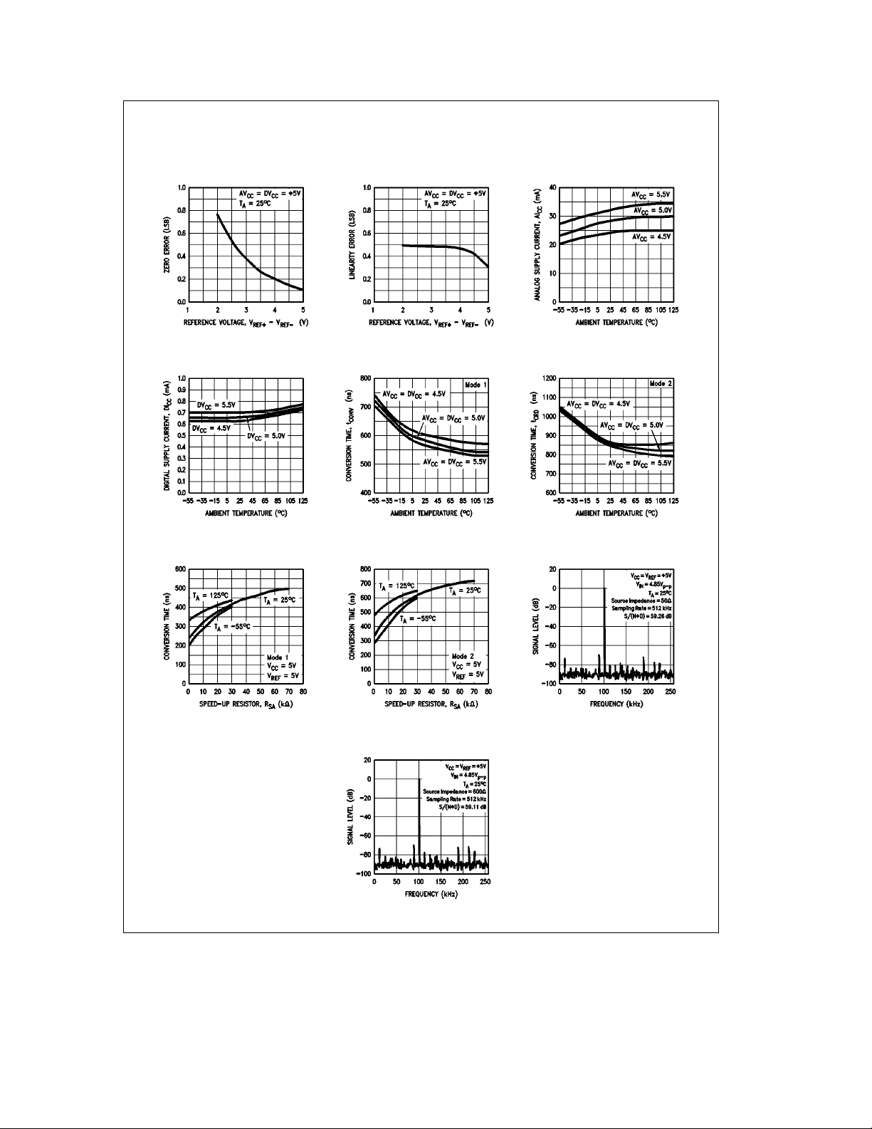
Typical Performance Characteristics
Zero (Offset) Error
vs Reference Voltage
Digital Supply Current
vs Temperature
Conversion Time
vs Speed-Up Resistor
(ADC10062 and ADC10064 Only)
Linearity Error
vs Reference Voltage
Conversion Time
vs Temperature
Conversion Time
vs Speed-Up Resistor
(ADC10062 and ADC10064 Only)
Analog Supply Current
vs Temperature
Conversion Time
vs Temperature
Spectral Response with
100 kHz Sine Wave Input
Spectral Response with
100 kHz Sine Wave Input
5
TL/H/11020– 2
Page 6
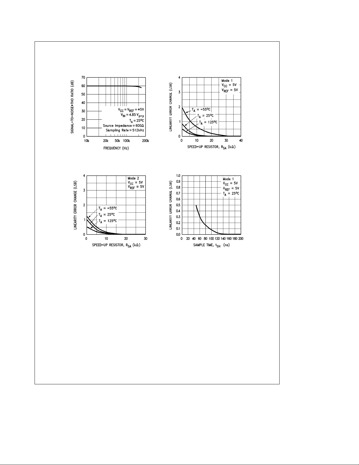
Typical Performance Characteristics (Continued)
Signal-to-Noise
vs Signal Frequency
Linearity Change
vs Speed-Up Resistor
(ADC10062 and ADC10064 Only)
a
THD Ratio
Linearity Change
vs Speed-Up Resistor
(ADC10062 and ADC10064 Only)
Linearity Error Change
vs Sample Time
TL/H/11020– 4
6
Page 7
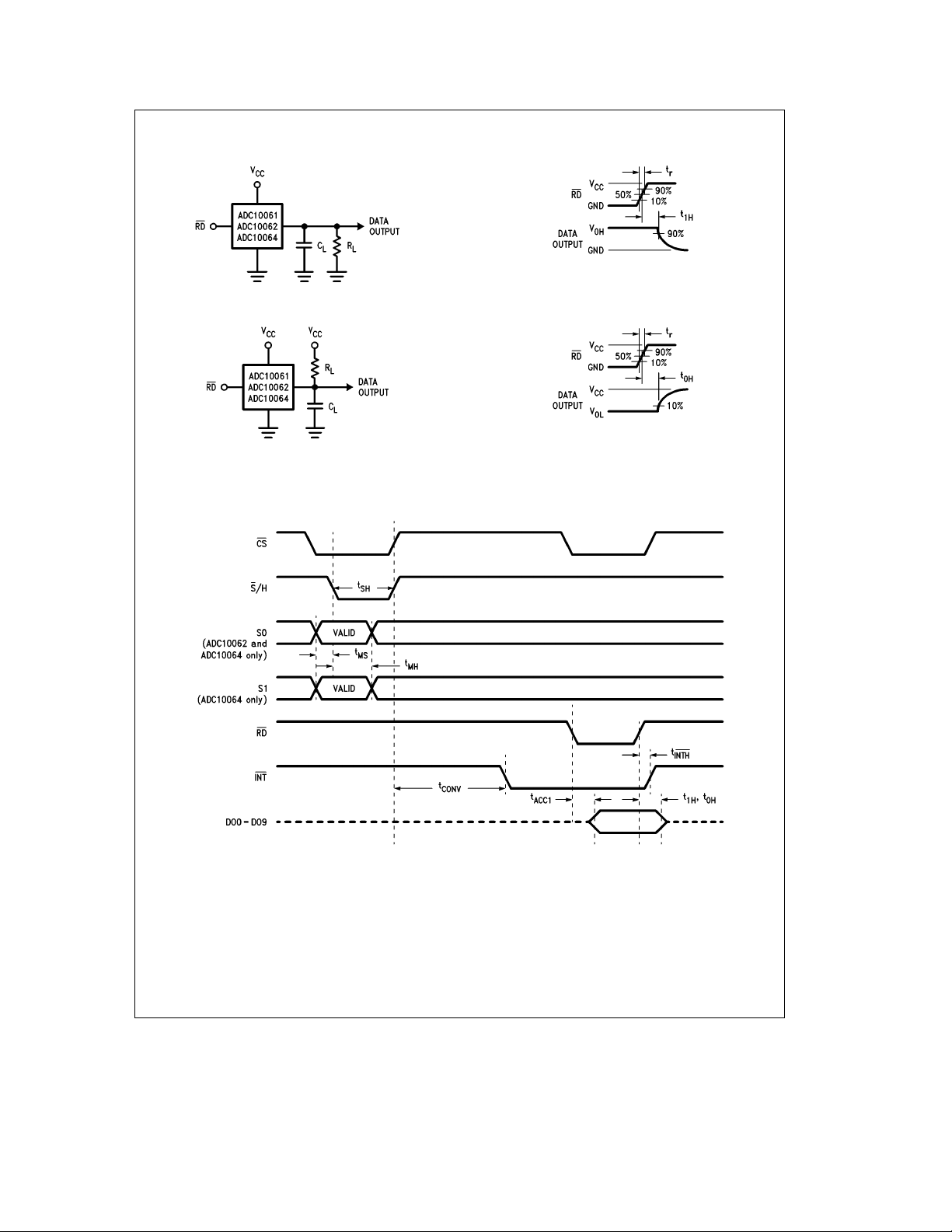
TRI-STATE Test Circuits and Waveforms
TL/H/11020– 5
TL/H/11020– 7
Timing Diagrams
TL/H/11020– 6
TL/H/11020– 8
FIGURE 1. Mode 1. The conversion time (t
7
) is set by the internal timer.
CONV
TL/H/11020– 9
Page 8
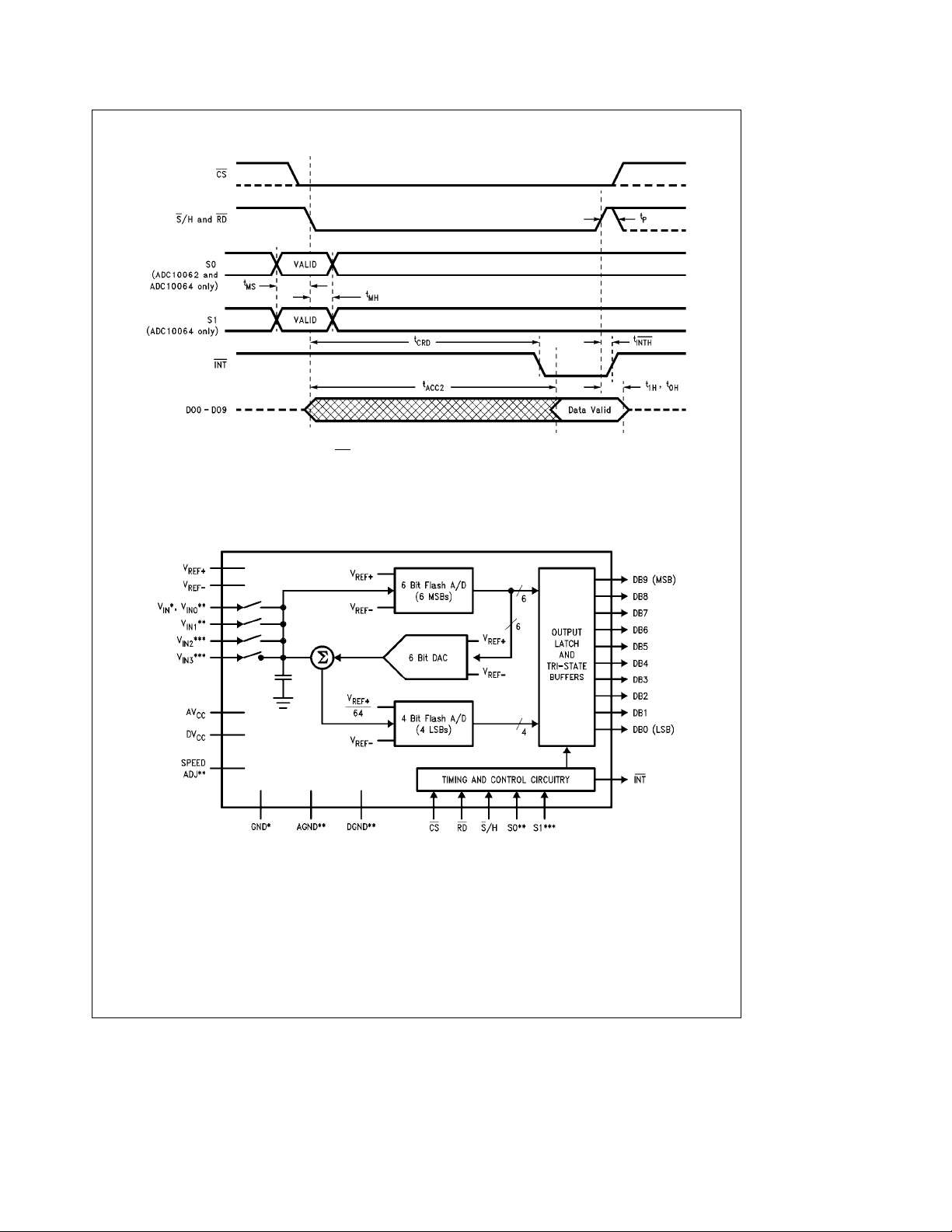
Timing Diagrams (Continued)
FIGURE 2. Mode 2 (RD Mode). The conversion time (t
sampling time and is determined by the internal timer.
Simplified Block Diagram
*ADC10061 Only
**ADC10062 and ADC10064 Only
***ADC10064 Only
) includes the
CRD
TL/H/11020– 10
TL/H/11020– 1
8
Page 9

Connection Diagrams
Dual-In-Line Package
TL/H/11020– 11
Dual-In-Line Package
Top View
Top View
Pin Descriptions
DVCC,AVCCThese are the digital and analog positive sup-
INT
/H This is the Sample/Hold control input. When
S
RD
CS
S0, S1 On the multiple-input devices (ADC10062
ply voltage inputs. They should always be
connected to the same voltage source, but
are brought out separately to allow for separate bypass capacitors. Each supply pin
should be bypassed with a 0.1 mF ceramic
capacitor in parallel with a 10 mF tantalum
capacitor to ground.
This is the active low interrupt output. INT
goes low at the end of each conversion, and
returns to a high state following the rising
edge of RD
this pin is forced low (and CS
.
is low), it causes the analog input signal to be sampled and
initiates a new conversion.
This is the active low Read control input.
When this RD
and CS are low, any data present in the output registers will be placed on
the data bus.
This is the active low Chip Select control input. When low, this pin enables the RD
S
/H pins.
and
and ADC10064), these pins select the analog
input that will be connected to the A/D during
the conversion. The input is selected based
on the state of S0 and S1 when S
/H makes
its High-to-Low transition (See the Timing Diagrams). The ADC10064 includes both S0
and S1. The ADC10062 includes just S0, and
the ADC10061 includes neither.
Dual-In-Line Package
TL/H/11020– 12
TL/H/11020– 13
Top View
V
,
b
REF
V
REF
V
IN,VIN0
V
IN1,VIN2
V
IN3
These are the reference voltage inputs. They
a
may be placed at any voltage between GND
and V
, but V
CC
V
. An input voltage equal to V
b
REF
produces an output code of 0, and an input
voltage equal to (V
an output code of 1023.
must be greater than
a
REF
b
1 LSB) produces
a
REF
, These are the analog input pins. The
, ADC10061 has one input (VIN), the
ADC10062 has two inputs (V
and the ADC10064 has four inputs (V
V
source should be less than 500X for best ac-
IN1,VIN2
and V
). The impedance of the
IN3
IN0
and V
REF
IN1
IN0
curacy and conversion speed. For accurate
conversions, no input pin (even one that is
not selected) should be driven more than
50 mV above V
or 50 mV below ground.
CC
GND, AGND, These are the power supply ground pins. The
DGND ADC10061 has a single ground pin (GND),
and the ADC10062 and ADC10064 have separate analog and digital ground pins (AGND
and DGND) for separate bypassing of the analog and digital supplies. The ground pins
should be connected to a stable, noise-free
system ground. For the devices with two
ground pins, both pins should be returned to
the same potential.
DB0–DB9 These are the TRI-STATE output pins.
SPEED ADJ (ADC10062 and ADC10064 only). This pin is
normally left unconnected, but by connecting
a resistor between this pin and ground, the
conversion time can be reduced. See the
Typical Performance Curves and the table of
Electrical Characteristics.
b
),
,
9
Page 10

Functional Description
The ADC10061, ADC10062 and ADC10064 digitize an analog input signal to 10 bits accuracy by performing two lowerresolution ‘‘flash’’ conversions. The first flash conversion
provides the six most significant bits (MSBs) of data, and
the second flash conversion provides the four least significant bits LSBs).
Figure 3
is a simplified block diagram of the converter. Near
the center of the diagram is a string of resistors. At the
bottom of the string of resistors are 16 resistors, each of
which has a value 1/1024 the resistance of the whole resistor string. These lower 16 resistors (the LSB Ladder) therefore have a voltage drop of 16/1024, or 1/64 of the total
reference voltage (V
mainder of the resistor string is made up of eight groups of
eight resistors connected in series. These comprise the
MSB Ladder. Each section of the MSB Ladder has (/8 of the
total reference voltage across it, and each of the LSB resistors has 1/64 of the total reference voltage across it. Tap
points across these resistors can be connected, in groups
of sixteen, to the sixteen comparators at the right of the
diagram.
On the left side of the diagram is a string of seven resistors
connected between V
compare the input voltage with the tap voltages on this resistor string to provide a low-resolution ‘‘estimate’’ of the
input voltage. This estimate is then used to control the multiplexer that connects the MSB Ladder to the sixteen comparators on the right. Note that the comparators on the left
needn’t be very accurate; they simply provide an estimate of
the input voltage. Only the sixteen comparators on the right
and the six on the left are necessary to perform the initial
six-bit flash conversion, instead of the 64 comparators that
would be required using conventional half-flash methods.
REF
REF
b
V
a
a
) across them. The re-
b
REF
and V
. Six comparators
b
REF
To perform a conversion, the estimator compares the input
voltage with the tap voltages on the seven resistors on the
left. The estimator decoder then determines which MSB
Ladder tap points will be connected to the sixteen comparators on the right. For example, assume that the estimator
determines that V
The estimator decoder will instruct the comparator MUX to
is between 11/16 and 13/16 of V
IN
REF
connect the 16 comparators to the taps on the MSB ladder
between 10/16 and 14/16 of V
then perform the first flash conversion. Note that since the
. The 16 comparators will
REF
comparators are connected to ladder voltages that extend
beyond the range indicated by the estimator circuit, errors in
the estimator as large as 1/16 of the reference voltage
(64 LSBs) will be corrected. This first flash conversion produces the six most significant bits of dataÐfour bits in the
flash itself, and 2 bits in the estimator.
The remaining four LSBs are now determined using the
same sixteen comparators that were used for the first flash
conversion. The MSB Ladder tap voltage just below the input voltage (as determined by the first flash) is subtracted
from the input voltage and compared with the tap points on
the sixteen LSB Ladder resistors. The result of this second,
four-bit flash conversion is then decoded, and the full 10-bit
result is latched.
Note that the sixteen comparators used in the first flash
conversion are reused for the second flash. Thus, the multistep conversion technique used in the ADC10061,
ADC10062, and ADC10064 needs only a small fraction of
the number of comparators that would be required for a
traditional flash converter, and far fewer than would be used
in a conventional half-flash approach. This allows the
ADC10061, ADC10062, and ADC10064 to perform highspeed conversions without excessive power drain.
.
FIGURE 3. Block Diagram of the Multistep Converter Architecture
10
TL/H/11020– 14
Page 11

Applications Information
1.0 MODES OF OPERATION
The ADC10061, ADC10062, and ADC10064 have two basic
digital interface modes.
diagrams for the two modes. The ADC10062 and
ADC10064 have input multiplexers that are controlled by
the logic levels on pins S
Table I is a truth table showing how the input channnels are
assigned.
Mode 1
In this mode, the S
S
/H is pulled low for a minimum of 250 ns. This causes the
comparators in the ‘‘coarse’’ flash converter to become active. When S
/H goes high, the result of the coarse conversion is latched and the ‘‘fine’’ conversion begins. After
600 ns (typical), INT
results are latched and can be read by pulling RD
that CS
must be low to enable S/H or RD.CSis internally
‘‘ANDed’’ with S
when CS
RD
and S/H are low, and data is read when CS and
are low. INT is reset high on the rising edge of RD.
TABLE I. Input Multiplexer Programming
ADC10064 ADC10062
S
S
1
0
00V
01V
10V
11V
(a)
Mode 2
In Mode 2, also called ‘‘RD
are tied together. A conversion is initiated by pulling both
pins low. The A/D converter samples the input voltage and
causes the coarse comparators to become active. An internal timer then terminates the coarse conversion and begins
the fine conversion. 850 ns (typical) after S
pull low, INT
goes low, indicating that the conversion is
completed. Approximately 20 ns later the data appearing on
the TRI-STATE output pins will be valid. Note that data will
appear on these pins throughout the conversion, but until
INT
goes low the data at the output pins will be the result of
the previous conversion.
2.0 REFERENCE CONSIDERATIONS
The ADC10061, ADC10062, and ADC10064 each have two
reference inputs. These inputs, V
differential and define the zero to full-scale range of the
input signal. The reference inputs can be connected to span
the entire supply voltage range (V
VCC) for ratiometric applications, or they can be connected
to different voltages (as long as they are between ground
and V
) when other input spans are required. Reducing
CC
the overall V
tivity of the converter (e.g., if V
REF
Figure 1
and
Figure 2
and S1when S/H goes low.
0
are timing
/H pin controls the start of conversion.
goes low, indicating that the conversion
low. Note
/H and RD; the input voltage is sampled
Channel S
IN0
IN1
IN2
IN3
0
0V
1V
Channel
IN0
IN1
(b)
mode’’, the S/H and RD pins
/H and RD are
and V
a
REF
b
REF
span to less than 5V increases the sensi-
REF
e
2V, then 1 LSB
e
REF
0V, V
, are fully
b
REF
a
1.953 mV). Note, however, that linearity and offset errors
become larger when lower reference voltages are used.
See the Typical Performance Curves for more information.
For this reason, reference voltages less than 2V are not
recommended.
In most applications, V
ground, but it is often useful to have an input span that is
will simply be connected to
b
REF
offset from ground. This situation is easily accommodated
by the reference configuration used in the ADC10061,
ADC10062, and ADC10064. V
voltage other than ground as long as the voltage source
connected to this pin is capable of sinking the converter’s
reference current (12.5 mA Max
connected to a voltage other than ground, bypass it with
can be connected to a
b
REF
@
V
REF
multiple capacitors.
Since the resistance between the two reference inputs can
be as low as 400X, the voltage source driving the reference
inputs should have low output impedance. Any noise on either reference input is a potential cause of conversion errors, so each of these pins must be supplied with a clean,
low noise voltage source. Each reference pin should be bypassed with a 10 mF tantalum and a 0.1 mF ceramic.
3.0 THE ANALOG INPUT
The ADC10061, ADC10062, and ADC10064 sample the analog input voltage once every conversion cycle. When this
happens, the input is briefly connected to an impedance
approximately equal to 600X in series with 35 pF. Short-duration current spikes can therefore be observed at the analog input during normal operation. These spikes are normal
and do not degrade the converter’s performance.
Large source impedances can slow the charging of the
sampling capacitors and degrade conversion accuracy.
Therefore, only signal sources with output impedances less
than 500X should be used if rated accuracy is to be
achieved at the minimum sample time (250 ns maximum). If
the sampling time is increased, the source impedance can
be larger. If a signal source has a high output impedance, its
output should be buffered with an operational amplifier. The
operational amplifier’s output should be well-behaved when
driving a switched 35 pF/600X load. Any ringing or voltage
shifts at the op amp’s output during the sampling period can
result in conversion errors.
Correct conversion results will be obtained for input voltages greater than GND
b
50 mV and less than V
50 mV. Do not allow the signal source to drive the analog
input pin more than 300 mV higher than AV
more than 300 mV lower than GND. If an analog input pin is
forced beyond these voltages, the current flowing through
the pin should be limited to 5 mA or less to avoid permanent
e
damage to the IC. The sum of all the overdrive currents into
all pins must be less than 20 mA. When the input signal is
expected to extend more than 300 mV beyond the power
supply limits, some sourt of protection scheme should be
used. A simple network using diodes and resistors is shown
e
in
Figure 4
.
e
5V). If V
and DVCC,or
CC
REF
is
b
a
a
11
Page 12

Applications Information (Continued)
FIGURE 4. Typical Connection. Note the multiple bypass capacitors on the reference and power supply pins. If V
TL/H/11020– 15
is not grounded, it should also be bypassed to analog ground using multiple capacitors (see 5.0 ‘‘Power Supply
Considerations’’). AGND and DGND should be at the same potential. V
Pin 17 is normally left open, but optional ‘‘speedup’’ resistor R
4.0 INHERENT SAMPLE-AND-HOLD
Because the ADC10061, ADC10062, and ADC10064 sample the input signal once during each conversion, they are
capable of measuring relatively fast input signals without the
help of an external sample-hold. In a non-sampling successive-approximation A/D converter, regardless of speed, the
input signal must be stable to better than
g
1/2 LSB during
each conversion cycle or significant errors will result. Consequently, even for many relatively slow input signals, the
signals must be externally sampled and held constant during each conversion if a SAR with no internal sample-andhold is used.
Because they incorporate a direct sample/hold control input, the ADC10061, ADC10062, and ADC10064 are suitable
for use in DSP-based systems. The S
/H input allows synchronization of the A/D converter to the DSP system’s sampling rate and to other ADC10061s, ADC10062s, and
ADC10064s.
The ADC10061, ADC10062, and ADC10064 can perform
accurate conversions of input signals with frequency components from DC to over 160 kHz.
5.0 POWER SUPPLY CONSIDERATIONS
The ADC10061, ADC10062, and ADC10064 are designed
to operate from a
two supply pins, AV
rate external bypass capacitors for the analog and digital
a
5V (nominal) power supply. There are
and DVCC. These pins allow sepa-
CC
portions of the circuit. To guarantee accurate conversions,
the two supply pins should be connected to the same voltage source, and each should be bypassed with a 0.1 mF
ceramic capacitor in parallel with a 10 mF tantalum capacitor. Depending on the circuit board layout and other system
The ADC10061 has a single ground pin, and the ADC10062
and ADC10064 each have separate analog and digital
ground pins for separate bypassing of the analog and digital
supplies. The devices with separate analog and digital
ground pins should have their ground pins connected to the
same potential, and all grounds should be ‘‘clean’’ and free
of noise.
In systems with multiple power supplies, careful attention to
power supply sequencing may be necessary to avoid overdriving inputs. The A/D converter’s power supply pins
should be at the proper voltage before digital or analog signals are applied to any of the other pins.
6.0 LAYOUT AND GROUNDING
In order to ensure fast, accurate conversions from the
ADC10061, ADC10062, and ADC10064, it is necessary to
use appropriate circuit board layout techniques. The analog
ground return path should be low-impedance and free of
noise from other parts of the system. Noise from digital circuitry can be especially troublesome, so digital grounds
should always be separate from analog grounds. For best
performance, separate ground planes should be provided
for the digital and analog parts of the system.
All bypass capacitors should be located as close to the converter as possible and should connect to the converter and
to ground with short traces. The analog input should be isolated from noisy signal traces to avoid having spurious signals couple to the input. Any external component (e.g., a
filter capacitor) connected across the converter’s input
should be connected to a very clean ground return point.
Grounding the component at the wrong point will result in
reduced conversion accuracy.
is shown with an input protection network.
IN0
can be used to reduce the conversion time.
SA
considerations, more bypassing may be necessary.
REF
b
12
Page 13

Applications Information (Continued)
7.0 DYNAMIC PERFORMANCE
Many applications require the A/D converter to digitize AC
signals, but conventional DC integral and differential nonlinearity specifications don’t accurately predict the A/D converter’s performance with AC input signals. The important
specifications for AC applications reflect the converter’s
ability to digitize AC signals without significant spectral errors and without adding noise to the digitized signal. Dynamic characteristics such as signal-to-noise ratio (SNR) and
total harmonic distortion (THD), are quantitative measures
of this capability.
An A/D converter’s AC performance can be measured using Fast Fourier Transform (FFT) methods. A sinusoidal
waveform is applied to the A/D converter’s input, and the
transform is then performed on the digitized waveform. The
resulting spectral plot might look like the ones shown in the
typical performance curves. The large peak is the fundamental frequency, and the noise and distortion components
(if any are present) are visible above and below the fundamental frequency. Harmonic distortion components appear
at whole multiples of the input frequency. Their amplitudes
are combined as the square root of the sum of the squares
and compared to the fundamental amplitude to yield the
THD specification. Typical values for THD are given in the
table of Electrical Characteristics.
Signal-to-noise ratio is the ratio of the amplitude at the fundamental frequency to the rms value at all other frequencies, excluding any harmonic distortion components. Typical
values are given in the Electrical Characteristics table. An
alternative definition of signal-to-noise ratio includes the distortion components along with the random noise to yield a
signal-to-noise-plus-distortion ration, or S/(N
The THD and noise performance of the A/D converter will
change with the frequency of the input signal, with more
distortion and noise occurring at higher signal frequencies.
a
D).
One way of describing the A/D’s performance as a function
of signal frequency is to make a plot of ‘‘effective bits’’ versus frequency. An ideal A/D converter with no linearity errors or self-generated noise will have a signal-to-noise ratio
equal to (6.02n
of the A/D converter. A real A/D converter will have some
amount of noise and distortion, and the effective bits can be
found by:
where S/(NaD) is the ratio of signal to noise and distortion, which can vary with frequency.
As an example, an ADC10061 witha5V
wave input signal will typically have a signal-to-noise-plusdistortion ratio of 59.2 dB, which is equivalent to 9.53 effective bits. As the input frequency increases, noise and distortion gradually increase, yielding a plot of effective bits or
a
S/(N
8.0 SPEED ADJUST
In applications that require faster conversion times, the
Speed Adjust pin (pin 14 on the ADC10062, pin 17 on the
ADC10064) can significantly reduce the conversion time.
The speed adjust pin is connected to an on-chip current
source that determines the converter’s internal timing. By
connecting a resistor between the speed adjust pin and
ground as shown in
rent is increased, which reduces the conversion time. As an
example, an 18k resistor reduces the conversion time of a
typical part from 600 ns to 350 ns with no significant effect
on linearity. Using smaller resistors to further decrease the
conversion time is possible as well, although the linearity
will begin to degrade somewhat (see curves). Note that the
resistor value needed to obtain a given conversion time will
vary from part to part, so this technique will generally require
some ‘‘tweaking’’ to obtain satisfactory results.
a
1.8) dB, where n is the resolution in bits
S/(NaD) (dB)b1.8
n (effective)
D) as shown in the typical performance curves.
e
Figure 4
6.02
, the internal programming cur-
, 100 kHz sine
P-P
13
Page 14

Physical Dimensions inches (millimeters)
Order Number ADC10061CMJ/883
NS Package Number J20A
Order Number ADC10062CMJ/883
NS Package Number J24A
14
Page 15

Physical Dimensions inches (millimeters) (Continued)
Order Number ADC10064CMJ/883
NS Package Number J28A
Order Number ADC10061BIWM or ADC10061CIWM
NS Package Number M20B
15
Page 16

Physical Dimensions inches (millimeters) (Continued)
Order Number ADC10062BIWM or ADC10062CIWM
Order Number ADC10064BIWM or ADC10064CIWM
NS Package Number M24B
NS Package Number M28B
16
Page 17

Physical Dimensions inches (millimeters) (Continued)
Order Number ADC10061BIN or ADC10061CIN
Order Number ADC10062BIN or ADC10062CIN
NS Package Number N20A
NS Package Number N24A
17
Page 18
Physical Dimensions inches (millimeters) (Continued)
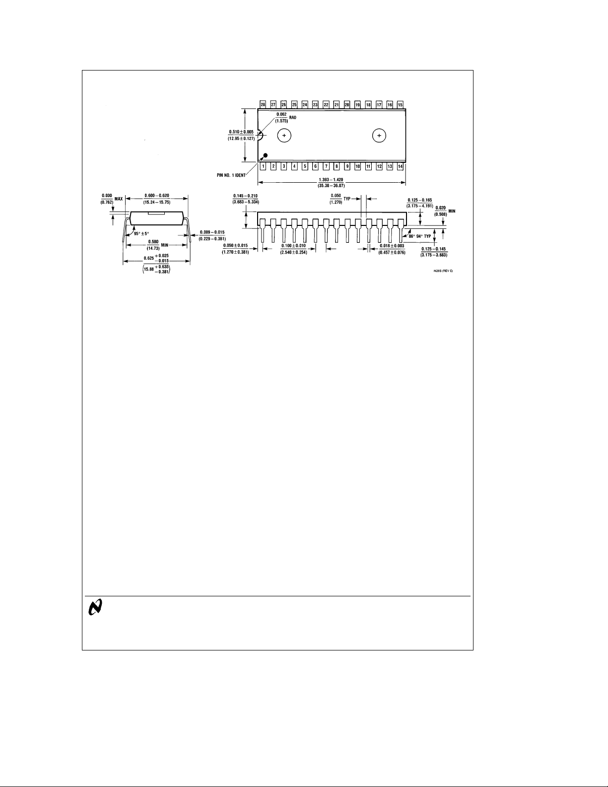
Order Number ADC10064BIN or ADC10064CIN
NS Package Number N28B
with Input Multiplexer and Sample/Hold
ADC10061/ADC10062/ADC10064 10-Bit 600 ns A/D Converter
LIFE SUPPORT POLICY
NATIONAL’S PRODUCTS ARE NOT AUTHORIZED FOR USE AS CRITICAL COMPONENTS IN LIFE SUPPORT
DEVICES OR SYSTEMS WITHOUT THE EXPRESS WRITTEN APPROVAL OF THE PRESIDENT OF NATIONAL
SEMICONDUCTOR CORPORATION. As used herein:
1. Life support devices or systems are devices or 2. A critical component is any component of a life
systems which, (a) are intended for surgical implant support device or system whose failure to perform can
into the body, or (b) support or sustain life, and whose be reasonably expected to cause the failure of the life
failure to perform, when properly used in accordance support device or system, or to affect its safety or
with instructions for use provided in the labeling, can effectiveness.
be reasonably expected to result in a significant injury
to the user.
National Semiconductor National Semiconductor National Semiconductor National Semiconductor National Semiconductores National Semiconductor
Corporation GmbH Japan Ltd. Hong Kong Ltd. Do Brazil Ltda. (Australia) Pty, Ltd.
2900 Semiconductor Drive Livry-Gargan-Str. 10 Sumitomo Chemical 13th Floor, Straight Block, Rue Deputado Lacorda Franco Building 16
P.O. Box 58090 D-82256 F4urstenfeldbruck Engineering Center Ocean Centre, 5 Canton Rd. 120-3A Business Park Drive
Santa Clara, CA 95052-8090 Germany Bldg. 7F Tsimshatsui, Kowloon Sao Paulo-SP Monash Business Park
Tel: 1(800) 272-9959 Tel: (81-41) 35-0 1-7-1, Nakase, Mihama-Ku Hong Kong Brazil 05418-000 Nottinghill, Melbourne
TWX: (910) 339-9240 Telex: 527649 Chiba-City, Tel: (852) 2737-1600 Tel: (55-11) 212-5066 Victoria 3168 Australia
National does not assume any responsibility for use of any circuitry described, no circuit patent licenses are implied and National reserves the right at any time without notice to change said circuitry and specifications.
Fax: (81-41) 35-1 Ciba Prefecture 261 Fax: (852) 2736-9960 Telex: 391-1131931 NSBR BR Tel: (3) 558-9999
Tel: (043) 299-2300 Fax: (55-11) 212-1181 Fax: (3) 558-9998
Fax: (043) 299-2500
 Loading...