

Page 1
ADVANCE INFORMATION
January 2005
ADC08D1000
High Performance, Low Power, Dual 8-Bit, 1 GSPS A/D
Converter
High Performance, Low Power, Dual 8-Bit, 1 GSPS A/D Converter
General Description
NOTE: This product is currently in development. – ALL
specifications are design targets and are subject to
change.
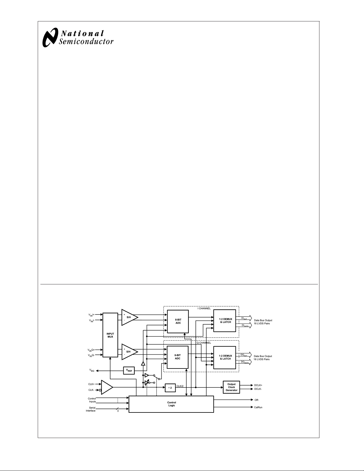
The ADC08D1000 is a dual, low power, high performance
CMOS analog-to-digital converter that digitizes signals to 8
bits resolution at sampling rates up to 1.3 GSPS. Consuming
a typical 1.6 Watts at 1 GSPS from a single 1.9 Volt supply,
this device is guaranteed to have no missing codes over the
full operating temperature range. The unique folding and
interpolating architecture, the fully differential comparator
design, the innovative design of the internal sample-andhold amplifier and the self-calibration scheme enable a very
flat response of all dynamic parameters beyond Nyquist,
producing a high 7.5 ENOB with a 500 MHz input signal and
a 1 GHz sample rate while providing a 10
formatting is offset binary and the LVDS digital outputs are
compliant with IEEE 1596.3-1996, with the exception of a
reduced common mode voltage of 0.8V.
Each converter has a 1:2 demultiplexer that feeds two LVDS
buses and reduces the output data rate on each bus to half
the sampling rate. The two converters can be interleaved
and used as a single 2 GSPS ADC.
The converter typically consumes less than 20 mW in the
Power Down Mode and is available in a 128-lead, thermally
enhanced exposed pad LQFP and operates over the industrial (-40˚C ≤ T
≤ +85˚C) temperature range.
A
-18
B.E.R. Output
Features
n Internal Sample-and-Hold
n Single +1.9V
n Choice of SDR or DDR output clocking
n Interleave Mode for 2x Sampling Rate
n Multiple ADC Synchronization Capability
n Guaranteed No Missing Codes
n Serial Interface for Extended Control
n Fine Adjustment of Input Full-Scale Range and Offset
n Duty Cycle Corrected Sample Clock
±
0.1V Operation
Key Specifications
n Resolution 8 Bits
n Max Conversion Rate 1 GSPS (min)
n Bit Error Rate 10
n ENOB
n DNL
n Power Consumption
@
500 MHz Input 7.5 Bits (typ)
±
— Operating 1.6 W (typ)
— Power Down Mode 20 mW (typ)
-18
(typ)
0.25 LSB (typ)
Applications
n Direct RF Down Conversion
n Digital Oscilloscopes
n Satellite Set-top boxes
n Communications Systems
n Test Instrumentation
Block Diagram
20097453
© 2005 National Semiconductor Corporation DS200974 www.national.com
Page 2
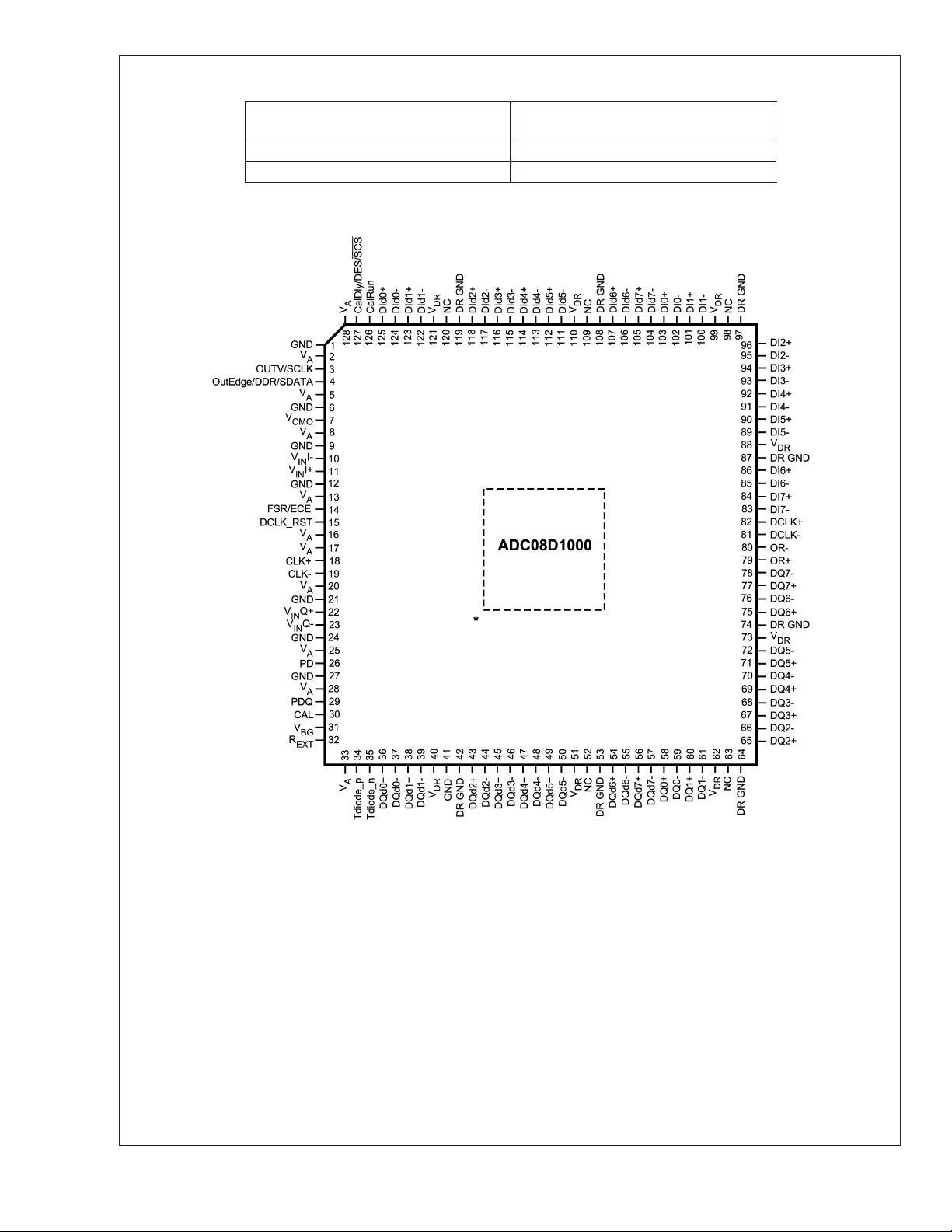
Ordering Information
ADC08D1000
Pin Configuration
Extended Commercial Temperature
<
<
T
Range (-40˚C
ADC08D1000CIYB 128-Pin Exposed Pad LQFP
ADC08D1000EVAL Evaluation Board
A
+85˚C)
NS Package
* Exposed pad on back of package must be soldered to ground plane to ensure rated performance.
www.national.com 2
20097401
Page 3
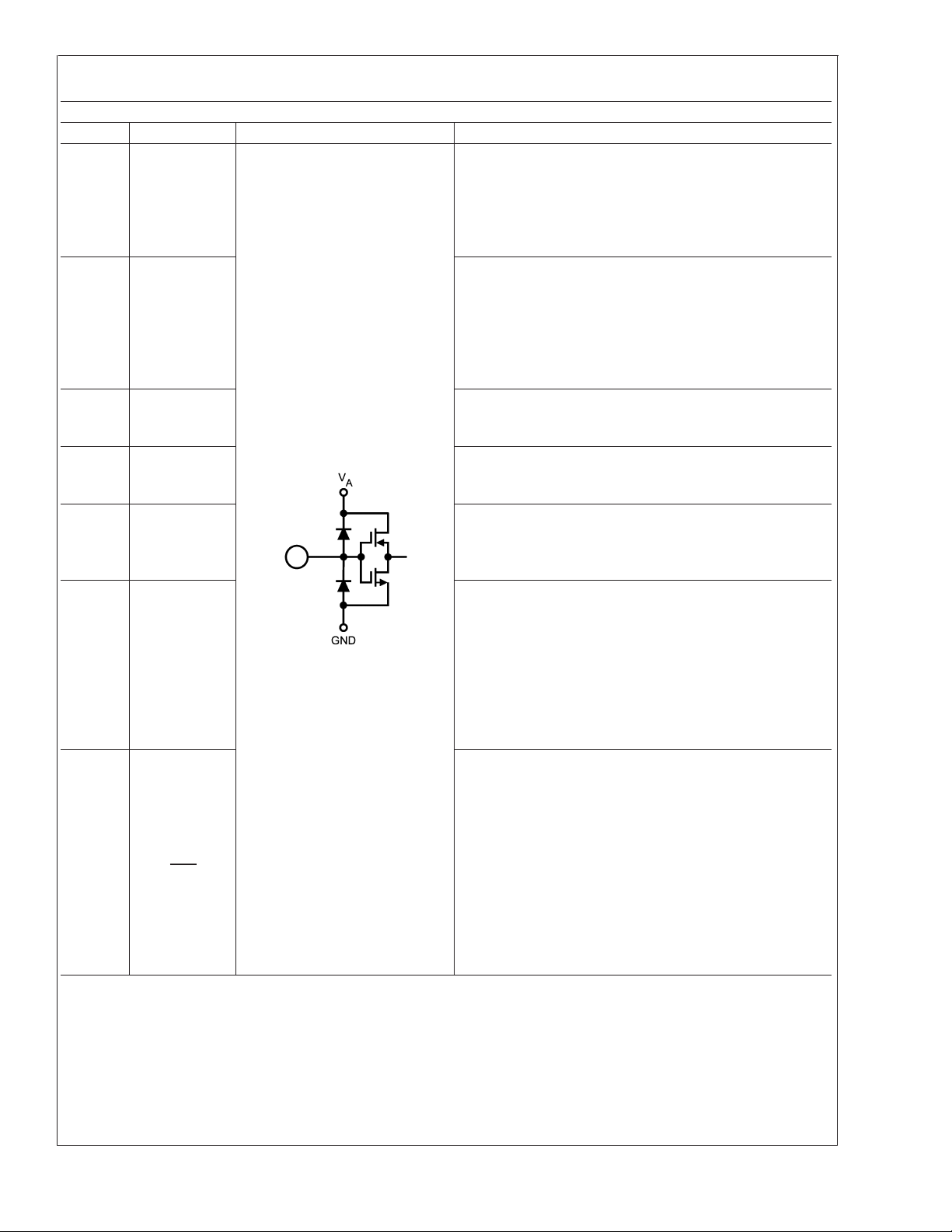
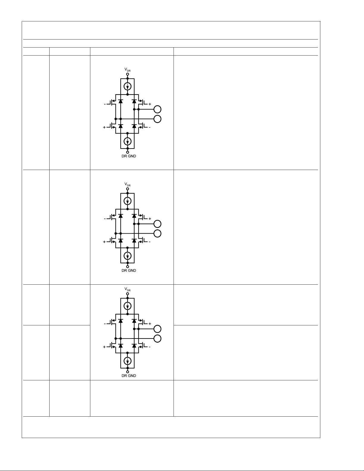
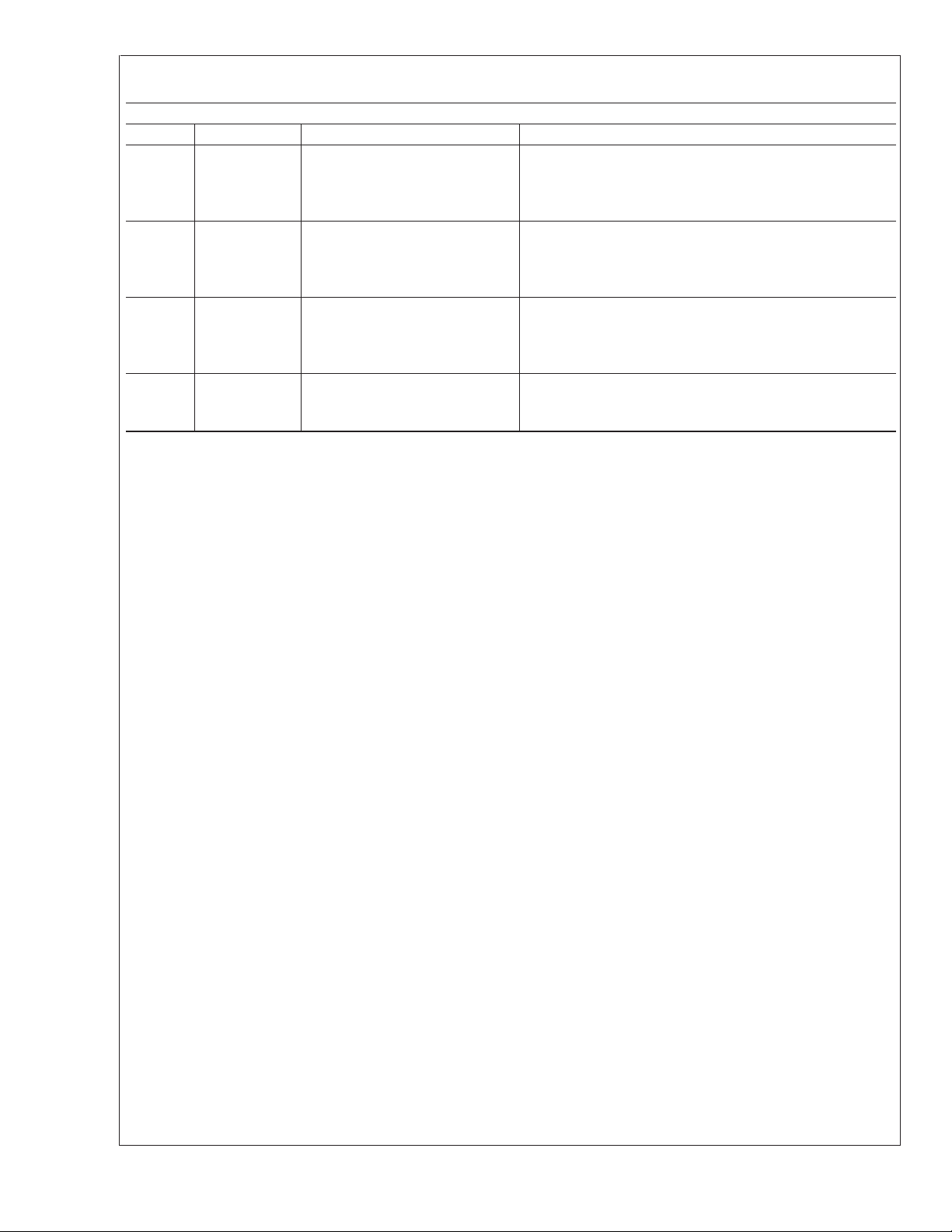
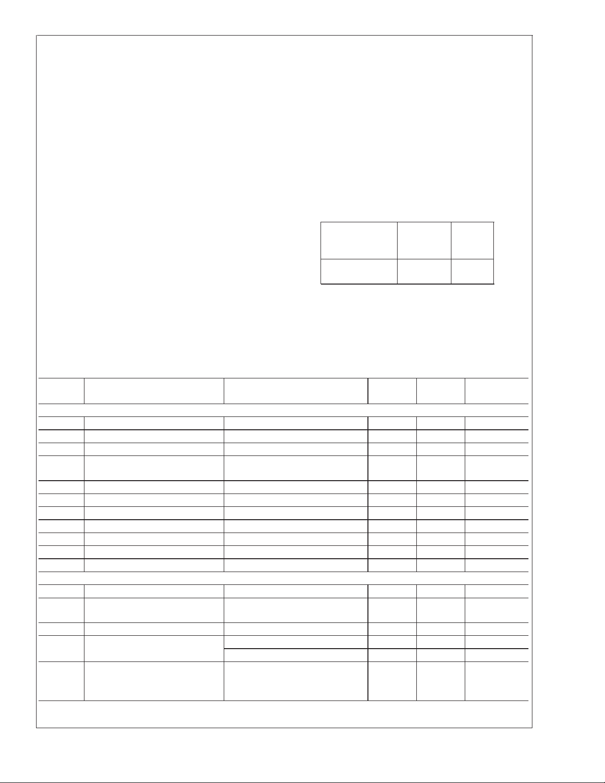
Pin Descriptions and Equivalent Circuits
Pin Functions
Pin No. Symbol Equivalent Circuit Description
Output Voltage Amplitude and Serial Interface Clock. Tie this
pin high for normal differential DCLK and data amplitude.
3 OutV / SCLK
OutEdge / DDR
4
/ SDATA
15 DCLK_RST
26
29
PD
PDQ
30 CAL
14 FSR/ECE
127
CalDly / DES /
SCS
Ground this pin for a reduced differential output amplitude and
reduced power consumption. See Section 1.1.6. When the
extended control mode is enabled, this pin functions as the
SCLK input which clocks in the serial data. See Section 1.3
DCLK Edge Select, Double Data Rate Enable and Serial Data
Input. This input sets the output edge of DCLK+ at which the
output data transitions. (See Section 1.1.5.2). When this pin is
floating or connected to 1/2 the supply voltage, DDR clocking
is enabled. When the extended control mode is enabled, this
pin functions as the (SDATA) input. See Section 1.2 for
details on the extended control mode.
DCLK Reset. A positive pulse on this pin is used to reset and
synchronize the DCLK outs of multiple converters. See
Section 1.5 for detailed description.
Power Down Pins. A logic high on the PD pin puts the entire
device into the Power Down Mode. A logic high on the PDQ
pin puts only the "Q" ADC into the Power Down mode.
Calibration Cycle Initiate. A minimum 80 input clock cycles
logic low followed by a minimum of 80 input clock cycles high
on this pin initiates the self calibration sequence. See Section
2.4.2.
Full Scale Range Select and Extended Control Enable. In
non-extended control mode, a logic low on this pin sets the
full-scale differential input range to 650 mV
this pin sets the full-scale differential input range to 860
. See Section 1.1.4. To enable the extended control
mV
P-P
mode, whereby the serial interface and control registers are
employed, allow this pin to float or connect it to a voltage
equal to V
/2. See Section 1.2 for information on the
A
extended control mode.
Calibration Delay, Dual Edge Sampling and Serial Interface
Chip Select. With a logic high or low on pin 14, this pin
functions as Calibration Delay and sets the number of input
clock cycles after power up before calibration begins (See
Section 1.1.1). With pin 14 floating, this pin acts as the enable
pin for the serial interface input and the CalDly value
becomes "0" (short delay with no provision for a long
power-up calibration delay). When this pin is floating or
connected to a voltage equal to V
Sampling) mode is selected where the "I" input is sampled at
twice the input clock rate and the "Q" input is ignored. See
Section 1.1.5.1.
. A logic high on
P-P
/2, DES (Dual Edge
A
ADC08D1000
www.national.com3
Page 4
Pin Descriptions and Equivalent Circuits (Continued)
Pin Functions
Pin No. Symbol Equivalent Circuit Description
ADC08D1000
18
19
11
10
.
22
23
7V
31 V
CLK+
CLK-
V
IN
V
IN
.
V
IN
V
IN
CMO
BG
I+
I−
Q+
Q−
126 CalRun
LVDS Clock input pins for the ADC. The differential clock
signal must be a.c. coupled to these pins. The input signal is
sampled on the falling edge of CLK+. See Section 2.3.
Analog signal inputs to the ADC. The differential full-scale
input range is 650 mV
when the FSR pin is high.
mV
P-P
when the FSR pin is low, or 860
P-P
Common Mode Voltage. The voltage output at this pin is
required to be the common mode input voltage at V
− when d.c. coupling is used. This pin should be grounded
V
IN
+ and
IN
when a.c. coupling is used at the analog inputs. This pin is
capable of sourcing or sinking 100µA. See Section 2.2.
Bandgap output voltage capable of 100 µA source/sink.
Calibration Running indication. This pin is at a logic high when
calibration is running.
32 R
34
35
www.national.com 4
EXT
Tdiode_P
Tdiode_N
External bias resistor connection. Nominal value is 3.3k-Ohms
±
0.1%) to ground. See Section 1.1.1.
(
Temperature Diode Positive (Anode) and Negative (Cathode)
for die temperature measurements. See Section 2.6.2.
Page 5
Pin Descriptions and Equivalent Circuits (Continued)
Pin Functions
Pin No. Symbol Equivalent Circuit Description
83/78
84/77
85/76
86/75
89/72
90/71
91/70
92/69
93/68
94/67
95/66
96/65
100/61
101/60
102/59
103/58
104/57
105/56
106/55
107/54
111/50
112/49
113/48
114/47
115/46
116/45
117/44
118/43
122/39
123/38
124/37
125/36
DI7− / DQ7−
DI7+ / DQ7+
DI6− / DQ6−
DI6+ / DQ6+
DI5− / DQ5−
DI5+ / DQ5+
DI4− / DQ4−
DI4+ / DQ4+
DI3− / DQ3−
DI3+ / DQ3+
DI2− / DQ2−
DI2+ / DQ2+
DI1− / DQ1−
DI1+ / DQ1+
DI0− / DQ0−
DI0+ / DQ0+
DId7− / DQd7−
DId7+ / DQd7+
DId6− / DQd6−
DId6+ / DQd6+
DId5− / DQd5−
DId5+ / DQd5+
DId4− / DQd4−
DId4+ / DQd4+
DId3− / DQd3−
DId3+ / DQd3+
DId2− / DQd2−
DId2+ / DQd2+
DId1− / DQd1−
DId1+ / DQd1+
DId0− / DQd0−
DId0+ / DQd0+
I and Q channel LVDS Data Outputs that are not delayed in
the output demultiplexer. Compared with the DId and DQd
outputs, these outputs represent the later time samples.
These outputs should always be terminated with a 100Ω
differential resistor.
I and Q channel LVDS Data Outputs that are delayed by one
CLK cycle in the output demultiplexer. Compared with the
DI/DQ outputs, these outputs represent the earlier time
sample. These outputs should always be terminated with a
100Ω differential resistor.
ADC08D1000
79
80
82
81
2, 5, 8,
13, 16,
17, 20,
25, 28,
33, 128
OR+
OR-
DCLK+
DCLK-
V
A
Out Of Range output. A differential high at these pins
indicates that the differential input is out of range (outside the
±
range
Differential Clock outputs used to latch the output data.
Delayed and non-delayed data outputs are supplied
synchronous to this signal. This signal is at 1/2 the input clock
rate in SDR mode and at 1/4 the input clock rate in the DDR
mode.
Analog power supply pins. Bypass these pins to ground.
300 mV or±400 mV as defined by the FSR pin).
www.national.com5
Page 6
Pin Descriptions and Equivalent Circuits (Continued)
Pin Functions
Pin No. Symbol Equivalent Circuit Description
ADC08D1000
40, 51
,62, 73,
88, 99,
110, 121
1, 6, 9,
12, 21,
24, 27,
41
42, 53,
64, 74,
87, 97,
108, 119
52, 63,
98, 109,
120
V
DR
GND Ground return for V
DR GND Ground return for V
NC No Connection. Make no connection to these pins.
Output Driver power supply pins. Bypass these pins to DR
GND.
.
A
.
DR
www.national.com 6
Page 7
ADC08D1000
Absolute Maximum Ratings
(Notes 1, 2)
If Military/Aerospace specified devices are required,
please contact the National Semiconductor Sales Office/
Distributors for availability and specifications.
Supply Voltage (V
Voltage on Any Input Pin −0.15V to (V
Ground Difference
|GND - DR GND| 0V to 100 mV
Input Current at Any Pin (Note 3)
Package Input Current (Note 3)
Power Dissipation at T
ESD Susceptibility (Note 4)
Human Body Model
Machine Model
Soldering Temperature, Infrared,
10 seconds (Note 5) 235˚C
Storage Temperature −65˚C to +150˚C
) 2.2V
A,VDR
= 25˚C 2.0 W
A
+0.15V)
±
25 mA
±
50 mA
2500V
250V
A
Operating Ratings (Notes 1, 2)
Ambient Temperature Range −40˚C ≤ T
Supply Voltage (V
Driver Supply Voltage (V
) +1.8V to +2.0V
A
) +1.8V to V
DR
Analog Input Common Mode
Voltage 1.2V to 1.3V
V
Differential Voltage Range −VFS/2 to +VFS/2
IN
Ground Difference
(|GND - DR GND|) 0V
CLK Pins Voltage Range 0V to V
Differential CLK Amplitude 0.6V
P-P
≤ +85˚C
A
to 2.0V
Package Thermal Resistance
θ
J-PAD
(Thermal
Pad)
Package
128-Lead Exposed
Pad LQFP
θ
(Top of
JC
Package)
10˚C / W 2.8˚C / W
Converter Electrical Characteristics
[Note: This product is currently in development. As such, the parameters specified in this section are DESIGN TARGETS. The specifications in this section cannot be guaranteed until device characterization has taken place.]
The following specifications apply after calibration for V
860mV
Extended Control Mode, R
to T
T
MIN
= 10 pF, Differential, a.c. coupled Sinewave Input Clock, f
P-P,CL
. All other limits TA= 25˚C, unless otherwise noted. (Notes 6, 7)
MAX
= 3300Ω±0.1%, Analog Signal Source Impedance = 100Ω. Boldface limits apply for TA=
EXT
A=VDR
Symbol Parameter Conditions
STATIC CONVERTER CHARACTERISTICS
INL Integral Non-Linearity
DNL Differential Non-Linearity
Resolution with No Missing Codes 8 Bits
V
OFF
V
OFF
TC V
Offset Error -0.45
_ADJ Input Offset Adjustment Range Extended Control Mode
Offset Error Tempco −40˚C to +85˚C −3 ppm/˚C
OFF
PFSE Positive Full-Scale Error (Note 9) −2.2
NFSE Negative Full-Scale Error (Note 9) −1.1
FS_ADJ Full-Scale Adjustment Range Extended Control Mode
TC PFSE Positive Full-Scale Error Tempco −40˚C to +85˚C 20 ppm/˚C
TC NFSE Negative Full-Scale Error Tempco −40˚C to +85˚C 13 ppm/˚C
Dynamic Converter Characteristics
FPBW Full Power Bandwidth Normal (non DES) Mode 1.7 GHz
FPBW
(DES)
Full Power Bandwidth Dual Edge Sampling Mode 900 MHz
B.E.R. Bit Error Rate 10
Gain Flatness
ENOB Effective Number of Bits
d.c. to 500 MHz
d.c. to 1 GHz
= 100 MHz, VIN= FSR − 0.5 dB 7.5 Bits
f
IN
f
= 248 MHz, VIN= FSR − 0.5 dB 7.5 TBD Bits (min)
IN
f
= 498 MHz, VIN= FSR − 0.5 dB 7.5 TBD Bits (min)
IN
= +1.9VDC, OutV = 1.9V, VINFSR (a.c. coupled) = differential
= 1 GHz at 0.5V
CLK
Typical
(Note 8)
with 50% duty cycle, Non-
P-P
Limits
(Note 8)
±
±
0.35
0.25
±
TBD LSB (max)
±
TBD LSB (max)
−TBD
TBD
±
45 mV
±
TBD mV (max)
±
TBD mV (max)
±
20
-18
±
0.5 dBFS
±
1.0 dBFS
±
15 %FS
(Limits)
LSB (min)
LSB (max)
Error/Bit
Units
A
A
P-P
www.national.com7
Page 8
Converter Electrical Characteristics (Continued)
[Note: This product is currently in development. As such, the parameters specified in this section are DESIGN TARGETS. The specifications in this section cannot be guaranteed until device characterization has taken place.]
The following specifications apply after calibration for V
ADC08D1000
860mV
Extended Control Mode, R
to T
T
MIN
= 10 pF, Differential, a.c. coupled Sinewave Input Clock, f
P-P,CL
. All other limits TA= 25˚C, unless otherwise noted. (Notes 6, 7)
MAX
= 3300Ω±0.1%, Analog Signal Source Impedance = 100Ω. Boldface limits apply for TA=
EXT
A=VDR
Symbol Parameter Conditions
STATIC CONVERTER CHARACTERISTICS
= 100 MHz, VIN= FSR − 0.5 dB 47 dB
f
SINAD
Signal-to-Noise Plus Distortion
Ratio
SNR Signal-to-Noise Ratio
THD Total Harmonic Distortion
2nd Harm Second Harmonic Distortion
3rd Harm Third Harmonic Distortion
SFDR Spurious-Free dynamic Range
IMD Intermodulation Distortion
Out of Range Output Code
(In addition to OR Output high)
IN
f
= 248 MHz, VIN= FSR − 0.5 dB 47 TBD dB (min)
IN
f
= 498 MHz, VIN= FSR − 0.5 dB 47 TBD dB (min)
IN
= 100 MHz, VIN= FSR − 0.5 dB 48 dB
f
IN
f
= 248 MHz, VIN= FSR − 0.5 dB 48 TBD dB (min)
IN
f
= 498 MHz, VIN= FSR − 0.5 dB 48 TBD dB (min)
IN
= 100 MHz, VIN= FSR − 0.5 dB -57 dB
f
IN
f
= 248 MHz, VIN= FSR − 0.5 dB -57 dB (max)
IN
f
= 498 MHz, VIN= FSR − 0.5 dB -57 dB (max)
IN
= 100 MHz, VIN= FSR − 0.5 dB −64 dB
f
IN
f
= 248 MHz, VIN= FSR − 0.5 dB −64 dB
IN
f
= 498 MHz, VIN= FSR − 0.5 dB −64 dB
IN
= 100 MHz, VIN= FSR − 0.5 dB −64 dB
f
IN
f
= 248 MHz, VIN= FSR − 0.5 dB −64 dB
IN
f
= 498 MHz, VIN= FSR − 0.5 dB −64 dB
IN
= 100 MHz, VIN= FSR − 0.5 dB 58.5 dB
f
IN
f
= 248 MHz, VIN= FSR − 0.5 dB 58.5 TBD dB (min)
IN
f
= 498 MHz, VIN= FSR − 0.5 dB 58.5 TBD dB (min)
IN
f
= 121 MHz, VIN=FSR−7dB
IN1
= 126 MHz, VIN=FSR−7dB
f
IN2
(V
+)−(VIN−)>+ Full Scale 255
IN
(V
+)−(VIN−)<− Full Scale 0
IN
ANALOG INPUT AND REFERENCE CHARACTERISTICS
V
IN
V
CMI
Full Scale Analog Differential Input
Range
Analog Input Common Mode
Voltage
Analog Input Capacitance, normal
C
IN
operation (Note 10)
Analog Input Capacitance, DES
Mode (Note 10)
R
IN
Differential Input Resistance 100
FSR pin 14 Low 650
FSR pin 14 High 860
Differential 0.02 pF
Each input pin to ground 1.6 pF
Differential 0.8 pF
Each input pin to ground 2.2 pF
ANALOG OUTPUT CHARACTERISTICS
V
CMO
TC V
C
LOAD
V
CMO
Common Mode Output Voltage 1.25
Common Mode Output Voltage
CMO
Temperature Coefficient
= −40˚C to +85˚C 118 ppm/˚C
T
A
Maximum VCMO load Capacitance 80 pF
= +1.9VDC, OutV = 1.9V, VINFSR (a.c. coupled) = differential
= 1 GHz at 0.5V
CLK
Typical
(Note 8)
with 50% duty cycle, Non-
P-P
Limits
(Note 8)
-51 dB
600 mV
700 mV
810 mV
910 mV
V
−50
V
CMO
CMO
+50
V
CMO
94 Ω (min)
106 Ω (max)
0.95
1.45
Units
(Limits)
(min)
P-P
(max)
P-P
(min)
P-P
(max)
P-P
mV (min)
mV (max)
V (min)
V (max)
www.national.com 8
Page 9
Converter Electrical Characteristics (Continued)
[Note: This product is currently in development. As such, the parameters specified in this section are DESIGN TARGETS. The specifications in this section cannot be guaranteed until device characterization has taken place.]
The following specifications apply after calibration for V
860mV
Extended Control Mode, R
to T
T
MIN
= 10 pF, Differential, a.c. coupled Sinewave Input Clock, f
P-P,CL
. All other limits TA= 25˚C, unless otherwise noted. (Notes 6, 7)
MAX
= 3300Ω±0.1%, Analog Signal Source Impedance = 100Ω. Boldface limits apply for TA=
EXT
A=VDR
Symbol Parameter Conditions
ANALOG OUTPUT CHARACTERISTICS
V
BG
TC V
C
LOAD
V
BG
Bandgap Reference Output
Voltage
Bandgap Reference Voltage
BG
Temperature Coefficient
Maximum Bandgap Reference load
Capacitance
=±100 µA 1.26
I
BG
TA= −40˚C to +85˚C,
=±100 µA
I
BG
TEMPERATURE DIODE CHARACTERISTICS
∆I
, 100 µA vs. 10 µA,
DIODE
= 25˚C
T
Temperature Diode Voltage
J
∆I
, 100 µA vs. 10 µA,
DIODE
= 85˚C
T
J
CHANNEL-TO-CHANNEL CHARACTERISTICS
Offset Match 2 TBD LSB (max)
Positive Full-Scale Match
Negative Full-Scale Match
X-TALK Crosstalk from I to Q Channel
X-TALK Crosstalk from Q to I Channel
Zero offset selected in Control
Register
Zero offset selected in Control
Register
Aggressor =867 MHz F.S.
Victim = 100 MHz F.S.
Aggressor =867 MHz F.S.
Victim = 100 MHz F.S.
CLOCK INPUT CHARACTERISTICS
Sine Wave Clock 0.6
V
ID
Differential Clock Input Level
Square Wave Clock 0.6
I
I
C
IN
Input Current VIN=0orVIN=V
Input Capacitance (Note 11)
Differential 0.02 pF
Each input to ground 1.5 pF
DIGITAL CONTROL PIN CHARACTERISTICS
V
IH
V
IL
I
I
C
IN
Logic High Input Voltage (Note 12) 1.4 V (min)
Logic Low Input Voltage (Note 12) 0.5 V (max)
=0orVIN=VA, Pins 4, 14, 127
V
Input Current
IN
V
=0orVIN=VA, All Other Pins
IN
Input Capacitance (Note 11) Each input to ground 1.2 pF
DIGITAL OUTPUT CHARACTERISTICS
OutV = V
V
OD
LVDS Differential Output Voltage
OutV = GND, measured
differentially
∆ V
V
O DIFF
OS
Change in LVDS Output Swing
Between Logic Levels
Output Offset Voltage 800 mV
= +1.9VDC, OutV = 1.9V, VINFSR (a.c. coupled) = differential
= 1 GHz at 0.5V
CLK
Typical
(Note 8)
with 50% duty cycle, Non-
P-P
Limits
(Note 8)
1.22
1.33
28 ppm/˚C
80 pF
TBD mV
TBD mV
6 TBD mV (max)
6 TBD mV (max)
-77 dB
-77 dB
0.4
2.0
0.4
2.0
±
A
, measured differentially 600
A
1µA
±
80 µA
±
1µA
400 mV
900 mV
450
±
1mV
280 mV
680 mV
Units
(Limits)
V (min)
V (max)
V
P-P
V
P-P
V
P-P
V
P-P
P-P
P-P
P-P
P-P
ADC08D1000
(min)
(max)
(min)
(max)
(min)
(max)
(min)
(max)
www.national.com9
Page 10
Converter Electrical Characteristics (Continued)
[Note: This product is currently in development. As such, the parameters specified in this section are DESIGN TARGETS. The specifications in this section cannot be guaranteed until device characterization has taken place.]
The following specifications apply after calibration for V
ADC08D1000
860mV
Extended Control Mode, R
to T
T
MIN
= 10 pF, Differential, a.c. coupled Sinewave Input Clock, f
P-P,CL
. All other limits TA= 25˚C, unless otherwise noted. (Notes 6, 7)
MAX
= 3300Ω±0.1%, Analog Signal Source Impedance = 100Ω. Boldface limits apply for TA=
EXT
A=VDR
Symbol Parameter Conditions
DIGITAL OUTPUT CHARACTERISTICS
∆ V
I
OS
Z
OS
O
Output Offset Voltage Change
Between Logic Levels
Output Short Circuit Current
Output+ & Output- connected to
0.8V
Differential Output Impedance 100 Ohms
POWER SUPPLY CHARACTERISTICS
PD = PDQ = Low
I
A
Analog Supply Current
PD = Low, PDQ = High
PD = High
PD = PDQ = Low
I
DR
Output Driver Supply Current
PD = Low, PDQ = High
PD = PDQ = High
PD = PDQ = Low
P
D
Power Consumption
PD = Low, PDQ = High
PD = PDQ = High
PSRR1 D.C. Power Supply Rejection Ratio
Change in Full Scale Error with
change in V
PSRR2 A.C. Power Supply Rejection Ratio 248 MHz, 50mV
AC ELECTRICAL CHARACTERISTICS
≤ 85˚C 1.1 1.0 GHz (min)
T
f
CLK1
f
CLK2
t
CL
t
CH
Maximum Conversion Rate
Minimum Conversion Rate 200 MHz
Input Clock Duty Cycle
Input Clock Duty Cycle
Input Clock Low Time (Note 12) 500 200 ps (min)
Input Clock High Time (Note 12) 500 200 ps (min)
A
T
≤ 75˚C 1.3 GHz
A
200 MHz ≤ Input clock frequency ≤
1 GHz (Normal Mode)
500MHz ≤ Input clock frequency ≤ 1
GHz (DES Mode)
DCLK Duty Cycle (Note 12) 50
t
RS
t
RH
t
SD
t
RPW
t
LHT
t
HLT
Reset Setup Time (Note 12) 150 TBD ps (min)
Reset Hold Time (Note 12) 250 TBD ps (min)
Syncronizing Edge to DCLK Output
Delay
f
CLKIN
f
CLKIN
= 1.0 GHz
= 200 MHz
Reset Pulse Width 4
Differential Low to High Transition
Time
Differential High to Low Transition
Time
10% to 90%, C
10% to 90%, C
50% of DCLK transition to 50% of
t
OSK
DCLK to Data Output Skew
Data transition, SDR Mode
and DDR Mode, 0˚ DCLK (Note 12)
t
SU
Data to DCLK Set-Up Time DDR Mode, 180˚ DCLK (Note 12) 750 TBD ps (min)
= +1.9VDC, OutV = 1.9V, VINFSR (a.c. coupled) = differential
= 1 GHz at 0.5V
CLK
Typical
(Note 8)
with 50% duty cycle, Non-
P-P
Limits
(Note 8)
±
1mV
±
4mA
627
325
690
360
4.3
202
116
257
135
1
1.6
0.84
1.8
0.94
20
from 1.8V to 2.0V
A
riding on V
P-P
A
73 dB
TBD dB
50
50
20
80
20
80
45
55
3.53
3.85
= 2.5 pF 250 ps
L
= 2.5 pF 250 ps
L
±
50
±
200 ps (max)
Units
(Limits)
mA (max)
mA
mA
mA (max)
mA (max)
mA
W (max)
W
mW
% (min)
% (max)
% (min)
% (max)
% (min)
% (max)
ns
Clock Cycles
(min)
www.national.com 10
Page 11

Converter Electrical Characteristics (Continued)
[Note: This product is currently in development. As such, the parameters specified in this section are DESIGN TARGETS. The specifications in this section cannot be guaranteed until device characterization has taken place.]
The following specifications apply after calibration for V
860mV
Extended Control Mode, R
to T
T
MIN
= 10 pF, Differential, a.c. coupled Sinewave Input Clock, f
P-P,CL
. All other limits TA= 25˚C, unless otherwise noted. (Notes 6, 7)
MAX
= 3300Ω±0.1%, Analog Signal Source Impedance = 100Ω. Boldface limits apply for TA=
EXT
A=VDR
Symbol Parameter Conditions
AC ELECTRICAL CHARACTERISTICS
t
H
t
AD
t
AJ
t
OD
DCLK to Data Hold Time DDR Mode, 180˚ DCLK (Note 12) 750 TBD ps (min)
Sampling (Aperture) Delay
Input CLK+ Fall to Acquisition of
Data
Aperture Jitter 0.4 ps rms
Input Clock to Data Output Delay
50% of Input Clock transition to
50% of Data transition
DI Outputs 13
DId Outputs 14
Pipeline Delay (Latency)
(Note 11)
DQ Outputs
DQd Outputs
Differential V
0V to get accurate conversion
t
WU
f
SCLK
t
SSU
t
SH
Over Range Recovery Time
PD low to Rated Accuracy
Conversion (Wake-Up Time)
Maximum Serial Clock Frequency 100 MHz
Data to Serial Clock Setup Time (Note 12) 2.5 TBD ns (min)
Data to Serial Clock Hold Time (Note 12) 1 TBD ns (min)
Serial Clock Low Time 4 ns (min)
Serial Clock High Time 4 ns (min)
t
CAL
t
CAL_L
t
CAL_H
Note 1: Absolute Maximum Ratings indicate limits beyond which damage to the device may occur. There is no guarantee of operation at the Absolute Maximum
Ratings. Operating Ratings indicate conditions for which the device is functional, but do not guarantee specific performance limits. For guaranteed specifications and
test conditions, see the Electrical Characteristics. The guaranteed specifications apply only for the test conditions listed. Some performance characteristics may
degrade when the device is not operated under the listed test conditions.
Note 2: All voltages are measured with respect to GND = DR GND = 0V, unless otherwise specified.
Note 3: When the input voltage at any pin exceeds the power supply limits (that is, less than GND or greater than V
25 mA. The 50 mA maximum package input current rating limits the number of pins that can safely exceed the power supplies with an input current of 25 mA to two.
This limit is not placed upon the power, ground and digital output pins.
Note 4: Human body model is 100 pF capacitor discharged through a 1.5 kΩ resistor. Machine model is 220 pF discharged through ZERO Ohms.
Note 5: See AN-450, “Surface Mounting Methods and Their Effect on Product Reliability”.
Note 6: The analog inputs are protected as shown below. Input voltage magnitudes beyond the Absolute Maximum Ratings may damage this device.
Calibration Cycle Time 1.4 x 10
CAL Pin Low Time See Figure 9 80
CAL Pin High Time See Figure 9 80
= +1.9VDC, OutV = 1.9V, VINFSR (a.c. coupled) = differential
= 1 GHz at 0.5V
CLK
Typical
(Note 8)
with 50% duty cycle, Non-
P-P
Limits
(Note 8)
Units
(Limits)
1.3 ns
3.1 ns
Normal Mode 13
DES Mode 13.5
Input Clock
Cycles
Normal Mode 14
DES Mode 14.5
step from±1.2V to
IN
TBD ns
500 ns
5
Clock Cycles
Clock Cycles
Clock Cycles
), the current at that pin should be limited to
A
(min)
(min)
ADC08D1000
www.national.com11
Page 12

Converter Electrical Characteristics (Continued)
ADC08D1000
20097404
Note 7: To guarantee accuracy, it is required that VAand VDRbe well bypassed. Each supply pin must be decoupled with separate bypass capacitors. Additionally,
achieving rated performance requires that the backside exposed pad be well grounded.
Note 8: Typical figures are at T
Level).
Note 9: Calculation of Full-Scale Error for this device assumes that the actual reference voltage is exactly its nominal value. Full-Scale Error for this device,
therefore, is a combination of Full-Scale Error and Reference Voltage Error. See Figure 2. For relationship between Gain Error and Full-Scale Error, see Specification
Definitions for Gain Error.
Note 10: The analog and clock input capacitances are die capacitances only. Additional package capacitances of 0.65 pF differential and 0.95 pF each pin to ground
are isolated from the die capacitances by lead and bond wire inductances.
Note 11: This parameter is guaranteed by design and is not tested in production.
Note 12: This parameter is guaranteed by design and/or characterization and is not tested in production.
Note 13: The digital control pin capacitances are die capacitances only. Additional package capacitance of 1.6 pF each pin to ground are isolated from the die
capacitances by lead and bond wire inductances.
Note 14: Each of the two converters of the ADC08D1000 has two LVDS output buses, which each clock data out at one half the sample rate. The data at each bus
is clocked out at one half the sample rate. The second bus (D0 through D7) has a pipeline latency that is one Input Clock cycle less than the latency of the first bus
(Dd0 through Dd7).
= 25˚C, and represent most likely parametric norms. Test limits are guaranteed to National’s AOQL (Average Outgoing Quality
J
www.national.com 12
Page 13

Specification Definitions
APERTURE (SAMPLING) DELAY is that time required after
the fall of the clock input for the sampling switch to open. The
Sample/Hold circuit effectively stops capturing the input signal and goes into the “hold” mode the aperture delay time
) after the input clock goes low.
(t
AD
APERTURE JITTER (t
from sample to sample. Aperture jitter shows up as input
noise.
Bit Error Rate (B.E.R.) is the probability of error and is
defined as the probable number of errors per unit of time
divided by the number of bits seen in that amount of time. A
B.E.R. of 10
-18
corresponds to a statistical error in one bit
about every four (4) years.
CLOCK DUTY CYCLE is the ratio of the time that the clock
wave form is at a logic high to the total time of one clock
period.
DIFFERENTIAL NON-LINEARITY (DNL) is the measure of
the maximum deviation from the ideal step size of 1 LSB.
Measured at 1 GSPS with a ramp input.
EFFECTIVE NUMBER OF BITS (ENOB, or EFFECTIVE
BITS) is another method of specifying Signal-to-Noise and
Distortion Ratio, or SINAD. ENOB is defined as (SINAD −
1.76) / 6.02 and says that the converter is equivalent to a
perfect ADC of this (ENOB) number of bits.
FULL POWER BANDWIDTH (FPBW) is a measure of the
frequency at which the reconstructed output fundamental
drops 3 dB below its low frequency value for a full scale
input.
GAIN ERROR is the deviation from the ideal slope of the
transfer function. It can be calculated from Offset and FullScale Errors:
Positive Gain Error = Offset Error − Positive Full-Scale
Error
Negative Gain Error = −(Offset Error − Negative Full-
Scale Error)
Gain Error = Negative Full-Scale Error − Positive Full-
Scale Error = Positive Gain Error + Negative Gain Error
INTEGRAL NON-LINEARITY (INL) is a measure of the
deviation of each individual code from a straight line through
the input to output transfer function. The deviation of any
given code from this straight line is measured from the
center of that code value. The best fit method is used.
INTERMODULATION DISTORTION (IMD) is the creation of
additional spectral components as a result of two sinusoidal
frequencies being applied to the ADC input at the same time.
it is defined as the ratio of the power in the second and third
order intermodulation products to the power in one of the
original frequencies. IMD is usually expressed in dBFS.
LSB (LEAST SIGNIFICANT BIT) is the bit that has the
smallest value or weight of all bits. This value is
where VFSis the differential full-scale amplitude of 600 mV
or 800 mV as set by the FSR input and "n" is the ADC
resolution in bits, which is 8 for the ADC08D1000.
LVDS DIFFERENTIAL OUTPUT VOLTAGE ((V
absolute value of the difference between the V
outputs; each measured with respect to Ground.
) is the variation in aperture delay
AJ
n
/2
V
FS
) is the
OD
+&VD-
D
20097446
FIGURE 1.
LVDS OUTPUT OFFSET VOLTAGE (V
between the D+ and D- pins output voltage; ie., [(V
-)]/2.
V
D
) is the midpoint
OS
+) +(
D
MISSING CODES are those output codes that are skipped
and will never appear at the ADC outputs. These codes
cannot be reached with any input value.
MSB (MOST SIGNIFICANT BIT) is the bit that has the
largest value or weight. Its value is one half of full scale.
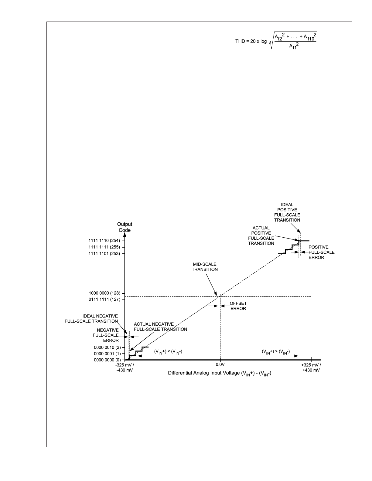
NEGATIVE FULL-SCALE ERROR (NFSE) is a measure of
how far the last code transition is from the ideal 1/2 LSB
above a differential −430 mV with the FSR pin high, or 1/2
LSB above a differential −325 mV with the FSR pin low. For
the ADC08D1000 the reference voltage is assumed to be
ideal, so this error is a combination of full-scale error and
reference voltage error.
OFFSET ERROR (V
) is a measure of how far the mid-
OFF
scale point is from the ideal zero voltage differential input.
Offset Error = Actual Input causing average of 8k
samples to result in an average code of 127.5.
OUTPUT DELAY (t
) is the time delay after the falling edge
OD
of DCLK before the data update is present at the output pins.
OVER-RANGE RECOVERY TIME is the time required after
±
the differential input voltages goes from
1.2V to 0V for the
converter to recover and make a conversion with its rated
accuracy.
PIPELINE DELAY (LATENCY) is the number of input clock
cycles between initiation of conversion and when that data is
presented to the output driver stage. New data is available at
every clock cycle, but the data lags the conversion by the
Pipeline Delay plus the t
OD
.
POSITIVE FULL-SCALE ERROR (PFSE) is a measure of
how far the last code transition is from the ideal 1-1/2 LSB
below a differential +430 mV with the FSR pin high, or 1-1/2
LSB below a differential +325 mV with the FSR pin low. For
the ADC08D1000 the reference voltage is assumed to be
ideal, so this error is a combination of full-scale error and
reference voltage error.
POWER SUPPLY REJECTION RATIO (PSRR) can be one
of two specifications. PSRR1 (DC PSRR) is the ratio of the
change in full-scale error that results from a power supply
voltage change from 1.8V to 2.0V. PSRR2 (AC PSRR) is a
measure of how well an a.c. signal riding upon the power
supply is rejected from the output and is measured with a
248 MHz, 50 mV
signal riding upon the power supply. It is
P-P
the ratio of the output amplitude of that signal at the output to
its amplitude on the power supply pin. PSRR is expressed in
dB.
ADC08D1000
www.national.com13
Page 14
Specification Definitions (Continued)
SIGNAL TO NOISE RATIO (SNR) is the ratio, expressed in
dB, of the rms value of the input signal at the output to the
rms value of the sum of all other spectral components below
ADC08D1000
one-half the sampling frequency, not including harmonics or
d.c.
SIGNAL TO NOISE PLUS DISTORTION (S/(N+D) or SINAD) is the ratio, expressed in dB, of the rms value of the
input signal at the output to the rms value of all of the other
spectral components below half the input clock frequency,
including harmonics but excluding d.c.
SPURIOUS-FREE DYNAMIC RANGE (SFDR) is the difference, expressed in dB, between the rms values of the input
signal at the output and the peak spurious signal, where a
spurious signal is any signal present in the output spectrum
that is not present at the input, excluding d.c.
TOTAL HARMONIC DISTORTION (THD) is the ratio expressed in dB, of the rms total of the first nine harmonic
levels at the output to the level of the fundamental at the
output. THD is calculated as
Transfer Characteristic
where Af1is the RMS power of the fundamental (output)
frequency and A
first 9 harmonic frequencies in the output spectrum.
– Second Harmonic Distortion (2nd Harm) is the difference, expressed in dB, between the RMS power in the input
frequency seen at the output and the power in its 2nd
harmonic level at the output.
– Third Harmonic Distortion (3rd Harm) is the difference
expressed in dB between the RMS power in the input frequency seen at the output and the power in its 3rd harmonic
level at the output.
through A
f2
are the RMS power of the
f10
FIGURE 2. Input / Output Transfer Characteristic
www.national.com 14
20097422
Page 15

Timing Diagrams
ADC08D1000
20097414
FIGURE 3. ADC08D1000 Timing — SDR Clocking
FIGURE 4. ADC08D1000 Timing — DDR Clocking
20097415
www.national.com15
Page 16

Timing Diagrams (Continued)
ADC08D1000
20097419
FIGURE 5. Serial Interface Timing
FIGURE 6. Clock Reset Timing in DDR Mode
FIGURE 7. Clock Reset Timing in SDR Mode with OUTEDGE Low
20097420
20097423
www.national.com 16
Page 17

Timing Diagrams (Continued)
FIGURE 8. Clock Reset Timing in SDR Mode with OUTEDGE High
ADC08D1000
20097424
FIGURE 9. Self Calibration and On-Command Calibration Timing
20097425
www.national.com17
Page 18

1.0 Functional Description
The ADC08D1000 is a versatile A/D Converter with an innovative architecture permitting very high speed operation. The
controls available ease the application of the device to circuit
ADC08D1000
solutions. Optimum performance requires adherence to the
provisions discussed here and in the Applications Information Section.
While it is generally poor practice to allow an active pin to
float, pins 4, 14 and 127 of the ADC08D1000 are designed to
be left floating without jeopardy. In all discussions throughout
this data sheet, whenever a function is called by allowing a
pin to float, connecting that pin to a potential of one half the
supply voltage will have the same effect as allowing it to
V
A
float.
1.1 OVERVIEW
The ADC08D1000 uses a calibrated folding and interpolating
architecture that achieves over 7.5 effective bits. The use of
folding amplifiers greatly reduces the number of comparators
and power consumption. Interpolation reduces the number
of front-end amplifiers required, minimizing the load on the
input signal and further reducing power requirements. In
addition to other things, on-chip calibration reduces the INL
bow often seen with folding architectures. The result is an
extremely fast, high performance, low power converter.
The analog input signal that is within the converter’s input
voltage range is digitized to eight bits at speeds of 200
MSPS to 1.3 GSPS, typical. Differential input voltages below
negative full-scale will cause the output word to consist of all
zeroes. Differential input voltages above positive full-scale
will cause the output word to consist of all ones. Either of
these conditions at either the "I" or "Q" input will cause the
OR (Out of Range) output to be activated. This single OR
output indicates when the output code from one or both of
the channels is below negative full scale or above positive
full scale.
Each of the two converters has a 1:2 demultiplexer that
feeds two LVDS output buses. The data on these buses
provide an output word rate on each bus at half the ADC
sampling rate and must be interleaved by the user to provide
output words at the full conversion rate.
The output levels may be selected to be normal or reduced.
Using reduced levels saves power but could result in erroneous data capture of some or all of the bits, especially at
higher sample rates and in marginally designed systems.
1.1.1 Self-Calibration
A self-calibration is performed upon power-up and can also
be invoked by the user upon command. Calibration trims the
100Ω analog input differential termination resistor and minimizes full-scale error, offset error, DNL and INL, resulting in
maximizing SNR, THD, SINAD (SNDR) and ENOB. Internal
bias currents are also set with the calibration process. All of
this is true whether the calibration is performed upon power
up or is performed upon command. Running the self calibration is an important part of this chip’s functionality and is
required in order to obtain adequate performance. In addition to the requirement to be run at power-up, self calibration
must be re-run whenever the sense of the FSR pin is
changed. For best performance, we recommend that self
calibration be run 20 seconds or more after application of
power and whenever the operating ambient temperature
changes more than 30˚C since calibration was last performed. See Section 2.4.2.2 for more information. Calibra-
tion can not be initiated or run while the device is in the
power-down mode. See Section 1.1.7 for information on the
interaction between Power Down and Calibration.
During the calibration process, the input termination resistor
is trimmed to a value that is equal to R
resistor is located between pin 32 and ground. R
±
3300 Ω
0.1%. With this value, the input termination resistor
is trimmed to be 100 Ω. Because R
/ 33. This external
EXT
EXT
is also used to set the
EXT
must be
proper current for the Track and Hold amplifier, for the
preamplifiers and for the comparators, other values of R
EXT
should not be used.
In normal operation, calibration is performed just after appli-
cation of power and whenever a valid calibration command
is given, which is holding the CAL pin low for at least 80 input
clock cycles, then hold it high for at least another 80 input
clock cycles. The time taken by the calibration procedure is
specified in the A.C. Characteristics Table. Holding the CAL
pin high upon power up will prevent the calibration process
from running until the CAL pin experiences the abovementioned 80 input clock cycles low followed by 80 cycles
high.
CalDly (pin 127) is used to select one of two delay times after
the application of power to the start of calibration. This
calibration delay is 2
1 GSPS) with CalDly low, or 2
25
input clock cycles (about 33.6 ms at
31
input clock cycles (about
2.15 seconds at 1 GSPS) with CalDly high. These delay
values allow the power supply to come up and stabilize
before calibration takes place. If the PD pin is high upon
power-up, the calibration delay counter will be disabled until
the PD pin is brought low. Therefore, holding the PD pin high
during power up will further delay the start of the power-up
calibration cycle. The best setting of the CalDly pin depends
upon the power-on settling time of the power supply.
The CalRun output is high whenever the calibration procedure is running. This is true whether the calibration is done at
power-up or on-command.
1.1.2 Acquiring the Input
Data is acquired at the falling edge of CLK+ (pin 18) and the
digital equivalent of that data is available at the digital outputs 13 input clock cycles later for the DI and DQ output
buses and 14 input clock cycles later for the DId and DQd
output buses. There is an additional internal delay called t
OD
before the data is available at the outputs. See the Timing
Diagram. The ADC08D1000 will convert as long as the input
clock signal is present. The fully differential comparator design and the innovative design of the sample-and-hold amplifier, together with self calibration, enables a very flat
SINAD/ENOB response beyond 1.0 GHz. The ADC08D1000
output data signaling is LVDS and the output format is offset
binary.
1.1.3 Control Modes
Much of the user control can be accomplished with several
control pins that are provided. Examples include initiation of
the calibration cycle, power down mode and full scale range
setting. However, the ADC08D1000 also provides an Extended Control mode whereby a serial interface is used to
access register-based control of several advanced features.
The Extended Control mode is not intended to be enabled
and disabled dynamically. Rather, the user is expected to
employ either the normal control mode or the Extended
Control mode at all times. When the device is in the Extended Control mode, pin-based control of several features
is replaced with register-based control and those pin-based
www.national.com 18
Page 19

1.0 Functional Description (Continued)
controls are disabled. These pins are OutV (pin 3), OutEdge/
DDR (pin 4), FSR (pin 14) and CalDly/DES (pin 127). See
Section 1.2 for details on the Extended Control mode.
The ADC08D1000 also has the option to use a duty cycle
corrected clock receiver as part of the input clock circuit. This
feature is enabled by default and provides improved ADC
clocking especially in the Dual-Edge Sampling mode (DES).
This circuitry allows the ADC to be clocked with a signal
source having a duty cycle ratio of 80 / 20 % (worst case) for
1.1.4 The Analog Inputs
The ADC08D1000 must be driven with a differential input
signal. Operation with a single-ended signal is not recommended. It is important that the inputs either be a.c. coupled
to the inputs with the V
the V
pin not grounded and an input common mode
CMO
voltage equal to the V
pin grounded or d.c. coupled with
CMO
output.
CMO
Two full-scale range settings are provided with pin 14 (FSR).
A high on pin 14 causes an input full-scale range setting of
860 mV
range setting of 650 mV
, while grounding pin 14 causes an input full-scale
P-P
. The full-scale range setting
P-P
operates equally on both ADCs.
In the Extended Control mode, the full-scale input range can
be set to values between 560 mV
and 840 mV
P-P
P-P
through
a serial interface. See Section 2.2
1.1.5 Clocking
The ADC08D1000 must be driven with an a.c. coupled,
differential clock signal. Section 2.3 describes the use of the
clock input pins. A differential LVDS output clock is available
for use in latching the ADC output data into whatever device
is used to receive the data.
The ADC08D1000 offers options for input and output clocking. These options include a choice of Dual Edge Sampling
(DES) or "interleaved mode" where the ADC08D1000 performs as a single device converting at twice the input clock
rate, a choice of which DCLK (DCLK) edge the output data
both the normal and the Dual Edge Sampling modes.
1.1.5.1 Dual-Edge Sampling
The DES mode allows one of the ADC08D1000’s inputs (I or
Q Channel) to be sampled by both ADCs. One ADC samples
the input on the positive edge of the input clock and the other
ADC samples the same input on the other edge of the input
clock. A single input is thus sampled twice per input clock
cycle, resulting in an overall sample rate of twice the input
clock frequency, or 2 GSPS with a 1 GHz input clock.
In this mode the outputs are interleaved such that the data is
effectively demultiplexed 4:1. Since the sample rate is
doubled, each of the 4 output buses have a 500 MSPS
output rate with a 1 GHz input clock. All data is available in
parallel. The four bytes of parallel data that are output with
each clock is in the following sampling order, from the earliest to the latest: DQd, DId, DQ, DI. Table 1 indicates what
the outputs represent for the various sampling possibilities.
In the non-extended mode of operation only the "I" input can
be sampled in the DES mode. In the extended mode of
operation the user can select which input is sampled.
The ADC08D1000 also includes an automatic clock phase
background calibration feature which can be used in DES
mode to automatically and continuously adjust the clock
phase of the I and Q channel. This feature removes the need
to adjust the clock phase setting manually and provides
optimal Dual-Edge Sampling ENOB performance.
transitions on, and a choice of Single Data Rate (SDR) or
Double Data Rate (DDR) outputs.
TABLE 1. Input Channel Samples Produced at Data Outputs
Data Outputs (Always
sourced with respect to
fall of DCLK)
DI
DId
DQ
DQd
Normal Sampling Mode
"I" Input Sampled with Fall
of CLK 13 cycles earlier.
"I" Input Sampled with Fall
of CLK 14 cycles earlier.
"Q" Input Sampled with Fall
of CLK 13 cycles earlier.
"Q" Input Sampled with Fall
of CLK 14 14 CLK cycles
after being sampled.
I-Channel Selected Q-Channel Selected *
"I" Input Sampled with Fall
of CLK 13 cycles earlier.
"I" Input Sampled with Fall
of CLK 14 cycles earlier.
"I" Input Sampled with Rise
of CLK 13.5 cycles earlier.
"I" Input Sampled with Rise
of CLK 14.5 cycles earlier.
Dual-Edge Sampling Mode
"Q" Input Sampled with Fall
of CLK 13 cycles earlier.
"Q" Input Sampled with Fall
of CLK 14 cycles earlier.
"Q" Input Sampled with Rise
of CLK 13.5 cycles earlier.
"Q" Input Sampled with Rise
of CLK 14.5 cycles earlier.
* Note that, in the Dual-Edge Sampling (DES) mode, the "Q" channel input can only be selected for sampling in the
Extended Control Mode.
ADC08D1000
1.1.5.2 OutEdge Setting
To help ease data capture in the SDR mode, the output data
may be caused to transition on either the positive or the
negative edge of the output data clock (DCLK). This is
chosen with the OutEdge input (pin 4). A high on the OutEdge input causes the output data to transition on the rising
edge of DCLK, while grounding this input causes the output
to transition on the falling edge of DCLK. See Section 2.4.3.
1.1.5.3 Double Data Rate
A choice of single data rate (SDR) or double data rate (DDR)
output is offered. With single data rate the output clock
(DCLK) frequency is the same as the data rate of the two
output buses. With double data rate the DCLK frequency is
half the data rate and data is sent to the outputs on both
input clock edges. DDR clocking is enabled by allowing pin 4
to float.
www.national.com19
Page 20
1.0 Functional Description (Continued)
1.1.6 The LVDS Outputs
The data outputs, the Out Of Range (OR) and DCLK, are
LVDS. Output current sources provide 3 mA of output current
ADC08D1000
to a differential 100 Ohm load when the OutV input (pin 14)
is high or 2.2 mA when the OutV input is low. For short LVDS
lines and low noise systems, satisfactory performance may
be realized with the OutV input low, which results in lower
power consumption. If the LVDS lines are long and/or the
system in which the ADC08D1000 is used is noisy, it may be
necessary to tie the OutV pin high.
If the PD input is brought high while a calibration is running,
the device will not go into power down until the calibration
sequence is complete. However, if power is applied and PD
is already high, the device will not begin the calibration
sequence until the PD input goes low. If a manual calibration
is requested while the device is powered down, the calibration will not begin at all. That is, the manual calibration input
is completely ignored in the power down state. Calibration
will function with the "Q" channel powered down, but that
channel will not be calibrated if PDQ is high. If the "Q"
channel is subsequently to be used, it is necessary to perform a calibration after PDQ is brought low.
1.1.7 Power Down
The ADC08D1000 is in the active state when the Power
Down pin (PD) is low. When the PD pin is high, the device is
in the power down mode. In this power down mode the data
output pins (positive and negative) are put into a high impedance state and the devices power consumption is reduced to
a minimal level. The DCLK+/- and OR +/- are not tri-stated,
they are weakly pulled down to ground internally. Therefore
when both I and Q are powered down the DCLK +/- and OR
+/- should not be terminated to a DC voltage.
A high on the PDQ pin will power down the "Q" channel and
leave the "I" channel active. There is no provision to power
down the "I" channel independently of the "Q" channel. Upon
return to normal operation, the pipeline will contain meaningless information.
TABLE 2. Features and modes
Feature Normal Control Mode Extended Control Mode
SDR or DDR Clocking Selected with pin 4
DDR Clock Phase Not Selectable (0˚ Phase Only)
SDR Data transitions with rising or
falling DCLK edge
LVDS output level Selected with pin 3
Power-On Calibration Delay Delay Selected with pin 127 Short delay only.
Full-Scale Range
Input Offset Adjust Not possible
Dual Edge Sampling Selection Enabled with pin 127 Enabled through DES Enable Register
Dual Edge Sampling Input Channel
Selection
DES Sampling Clock Adjustment
Selected with pin 4
Options (650 mV
selected with pin 14. Selected range
applies to both channels.
Only I-Channel Input can be used
The Clock Phase is adjusted
automatically
1.2 NORMAL/EXTENDED CONTROL
The ADC08D1000 may be operated in one of two modes. In
the simpler "normal" control mode, the user affects available
configuration and control of the device through several control pins. The "extended control mode" provides additional
configuration and control options through a serial interface
and a set of 8 registers. The two control modes are selected
with pin 14 (FSR/ECE: Extended Control Enable). The
choice of control modes is required to be a fixed selection
and is not intended to be switched dynamically while the
device is operational.
Table 2 shows how several of the device features are affected by the control mode chosen.
Selected with DE bit in the
Configuration Register
Selected with DCP bit in the
Configuration Register. See Section
1.4 REGISTER DESCRIPTION
Selected with the OE bit in the
Configuration Register
Selected with the OV bit in the
Configuration Register
Up to 512 step adjustments over a
or 860 mV
P-P
P-P
)
nominal range of 560 mV to 840 mV.
Separate range selected for I- and
Q-Channels. Selected using registers
3H and Bh
±
Separate
steps for each channel using registers
2h and Ah
Either I- or Q-Channel input may be
sampled by both ADCs
Automatic Clock Phase control can be
selected by setting bit 14 in the DES
Enable register (Dh). The clock phase
can also be adjusted manually through
the Coarse & Fine registers (Eh and
Fh)
45 mV adjustments in 512
www.national.com 20
Page 21

ADC08D1000
1.0 Functional Description (Continued)
The default state of the Extended Control Mode is set upon
power-on reset (internally performed by the device) and is
shown in Table 3.
TABLE 3. Extended Control Mode Operation (Pin 14
Floating)
Feature
SDR or DDR Clocking DDR Clocking
DDR Clock Phase
LVDS Output Amplitude
Calibration Delay Short Delay
Full-Scale Range
Input Offset Adjust
Dual Edge Sampling
(DES)
1.3 THE SERIAL INTERFACE
The 3-pin serial interface is enabled only when the device is
in the Extended Control mode. The pins of this interface are
Serial Clock (SCLK), Serial Data (SDATA) and Serial Interface Chip Select (SCS) Eight write only registers are accessible through this serial interface.
SCS: This signal should be asserted low while accessing a
register through the serial interface. Setup and hold times
with respect to the SCLK must be observed.
SCLK: Serial data input is accepted with the rising edge of
this signal.
SDATA: Each register access requires a specific 32-bit pattern at this input. This pattern consists of a header, register
address and register value. The data is shifted in MSB first.
Setup and hold times with respect to the SCLK must be
observed. See the Timing Diagram.
Each Register access consists of 32 bits, as shown in Figure
5 of the Timing Diagrams. The fixed header pattern is 0000
0000 0001 (eleven zeros followed by a 1). The loading
sequence is such that a "0" is loaded first. These 12 bits form
the header. The next 4 bits are the address of the register
that is to be written to and the last 16 bits are the data written
to the addressed register. The addresses of the various
registers are indicated in Table 4.
Refer to the Register Description (Section 1.4) for information on the data to be written to the registers.
Subsequent register accesses may be performed immediately, starting with the 33rd SCLK. This means that the SCS
input does not have to be deasserted and asserted again
between register addresses. It is possible, although not recommended, to keep the SCS input permanently enabled (at
a logic low) when using extended control.
Extended Control Mode
Default State
Data changes with DCLK
edge (0˚ phase)
Normal amplitude
(600 mV
700 mV nominal for both
channels
No adjustment for either
channel
Not enabled
P-P
)
TABLE 4. Register Addresses
4-Bit Address
Loading Sequence:
A3 loaded after H0, A0 loaded last
A3 A2 A1 A0 Hex Register Addressed
0 0 0 0 0h Reserved
0 0 0 1 1h Configuration
0 0 1 0 2h "I" Ch Offset
0 0 1 1 3h "I" Ch Full-Scale
Voltage Adjust
0 1 0 0 4h Reserved
0 1 0 1 5h Reserved
0 1 1 0 6h Reserved
0 1 1 1 7h Reserved
1 0 0 0 8h Reserved
1 0 0 1 9h Reserved
1 0 1 0 Ah "Q" Ch Offset
1 0 1 1 Bh "Q" Ch Full-Scale
Voltage Adjust
1 1 0 0 Ch Reserved
1 1 0 1 Dh DES Enable
1 1 1 0 Eh DES Coarse Adjust
1 1 1 1 Fh DES Fine Adjust
1.4 REGISTER DESCRIPTION
Eight write-only registers provide several control and configuration options in the Extended Control Mode. These registers have no effect when the device is in the Normal
Control Mode. Each register description below also shows
the Power-On Reset (POR) state of each control bit.
Configuration Register
Addr: 1h (0001b) W only (0xB2FF)
D15 D14 D13 D12 D11 D10 D9 D8
1 0 1 DCS DCP nDE OV OE
D7 D6 D5 D4 D3 D2 D1 D0
11111111
Bit 15 Must be set to 1b
Bit 14 Must be set to 0b
Bit 13 Must be set to 1b
Bit 12 DCS:Duty Cycle Stabilizer. When this bit is
set to 1b , a duty cycle stabilzation circuit is
applied to the clock input. When this bit is set
to 0b the stabilzation circuit is disabled.
POR State: 1b
Bit 11 DCP: DDR Clock Phase. This bit only has an
effect in the DDR mode. When this bit is set
to 0b, the DCLK edges are time-aligned with
the data bus edges ("0˚ Phase"). When this
bit is set to a 1b, the DCLK edges are placed
in the middle of the data bit-cells ("180˚
Phase").
POR State: 0b
www.national.com21
Page 22
1.0 Functional Description (Continued)
Bit 10 nDE: DDR Enable. When this bit is set to 0b,
data bus clocking follows the DDR (Dual
ADC08D1000
Bit 9 OV: Output Voltage. This bit determines the
Bit 8 OE: Output Edge. This bit selects the DCLK
Bits 7:0 Must be set to 1b.
Addr: 2h (0010b) W only (0x007F)
D15 D14 D13 D12 D11 D10 D9 D8
(MSB) Offset Value (LSB)
D7 D6 D5 D4 D3 D2 D1 D0
Sign 1111111
Bits 15:8 Offset Value. The input offset of the
Bit 7 Sign bit. 0b gives positive offset, 1b gives
Bit 6:0 Must be set to 1b
Data Rate) mode whereby a data word is
output with each rising and falling edge of
DCLK. When this bit is set to a 1b, data bus
clocking follows the SDR (single data rate)
mode whereby each data word is output with
either the rising or falling edge of DCLK , as
determined by the OutEdge bit.
POR State: 0b
LVDS outputs’ voltage amplitude and has the
same function as the OutV pin that is used in
the normal control mode. When this bit is set
to 1b, the "normal" output amplitude of 600
is used. When this bit is set to 0b, the
mV
P-P
reduced output amplitude of 450mV
used.
POR State: 1b
edge with which the data words transition in
the SDR mode and has the same effect as
the OutEdge pin in the normal control mode.
When this bit is 1, the data outputs change
with the rising edge of DCLK+. When this bit
is 0, the data output change with the falling
edge of DCLK+.
POR State: 0b
I-Channel Offset
I-Channel ADC is adjusted linearly and
monotonically by the value in this field. 00h
provides zero nominal offset, while FFh
±
provides a nominal
45 mV of offset. Thus,
each code step provides 0.176 mV of offset.
POR State: 0000 0000 b
negative offset.
POR State: 0b
P-P
I-Channel Full-Scale Voltage Adjust
Addr: 3h (0011b) W only (0x807F)
D15 D14 D13 D12 D11 D10 D9 D8
(MSB) Adjust Value
D7 D6 D5 D4 D3 D2 D1 D0
(LSB) 1111111
Bit 15:7 Full Scale Voltage Adjust Value. The input
full-scale voltage or gain of the I-Channel
ADC is adjusted linearly and monotonically
with a 9 bit data value. The adjustment range
±
20% of the nominal 700 mV
is
P-P
differential value.
0000 0000 0 560mV
1000 0000 0
700mV
DIFF
DIFF
Default Value
is
1111 1111 1 840mV
DIFF
For best performance, it is recommended
that the value in this field be limited to the
range of 0110 0000 0b to 1110 0000 0b. i.e.,
±
limit the amount of adjustment to
±
remaining
5% headroom allows for the
15%. The
ADC’s own full scale variation. A gain
adjustment does not require ADC
re-calibration.
POR State: 1 0000 0000 b (no adjustment)
Bits 6:0 Must be set to 1b
Q-Channel Offset
Addr: Ah (1010b) W only (0x007F)
D15 D14 D13 D12 D11 D10 D9 D8
(MSB) Offset Value (LSB)
D7 D6 D5 D4 D3 D2 D1 D0
Sign 1111111
Bit 15:8 Offset Value. The input offset of the
Q-Channel ADC is adjusted linearly and
monotonically by the value in this field. 00h
provides zero nominal offset, while FFh
±
provides a nominal
45 mV of offset. Thus,
each code step provides about 0.176 mV of
offset.
POR State: 0000 0000 b
Bit 7 Sign bit. 0b gives positive offset, 1b gives
negative offset.
POR State: 0b
Bit 6:0 Must be set to 1b
www.national.com 22
Page 23

ADC08D1000
1.0 Functional Description (Continued)
Q-Channel Full-Scale Voltage Adjust
Addr: Bh (1011b) W only (0x807F)
D15 D14 D13 D12 D11 D10 D9 D8
(MSB) Adjust Value
D7 D6 D5 D4 D3 D2 D1 D0
(LSB) 1111111
Bit 15:7 Full Scale Voltage Adjust Value. The input
full-scale voltage or gain of the I-Channel
ADC is adjusted linearly and monotonically
with a 9 bit data value. The adjustment
±
range is
differential value.
0000 0000 0 560mV
1000 0000 0 700mV
1111 1111 1 840mV
For best performance, it is recommended
that the value in this field be limited to the
range of 0110 0000 0b to 1110 0000 0b.
i.e., limit the amount of adjustment to
The remaining
the ADC’s own full scale variation. A gain
adjustment does not require ADC
re-calibration.
POR State: 1 0000 0000b (no adjustment)
Bits 6:0 Must be set to 1b
Addr: Dh (1101b) W only (0x3FFF)
D15 D14 D13 D12 D11 D10 D9 D8
DENACP111111
D7 D6 D5 D4 D3 D2 D1 D0
11111111
Bit 15 DES Enable. Setting this bit to 1b enables
the Dual Edge Sampling mode. In this mode
the ADCs in this device are used to sample
and convert the same analog input in a
time-interleaved manner, accomplishing a
sampling rate of twice the input clock rate.
When this bit is set to 1b, the device
operates in the normal dual channel mode.
POR State: 0b
20% of the nominal 700 mV
P-P
P-P
P-P
±
5% headroom allows for
DES Enable
P-P
±
15%.
Bit 14 Automatic Clock Phase Control. Setting this
bit to 1b enables the Automatic Clock Phase
Control. In this mode the DES Coarse and
Fine manual controls are disabled. A phase
detection circuit continually adjusts the I and
Q sampling edges to be 180 degrees out of
phase. When this bit is set to 1b, the
sample (input) clock delay between the I
and Q channels is set manually using the
DES Coarse and Fine Adjust registers. (See
Section 2.4.5 for important application
information)
POR State: 0b
Bits 13:0 Must be set to 1b
DES Coarse Adjust
Addr: Eh (1110b) W only (0x07FF)
D15 D14 D13 D12 D11 D10 D9 D8
IS ADS CAM 1 1 1
D7 D6 D5 D4 D3 D2 D1 D0
11111111
Bit 15 Input Select. When this bit is set to 0b the "I"
input is operated upon by both ADCs. When
this bit is set to 1b the "Q" input is operated
on by both ADCs.
POR State: 0b
Bit 14 Adjust Direction Select. When this bit is set
to "0", the "I" channel sample clock is
delayed while the "Q" channel sample clock
remains fixed. When this bit is set to "1", the
"Q" channel sample clock is delayed while
the "I" channel sample clock remains fixed.
POR State: 0b
Bits 13:11 Coarse Adjust Magnitude. Each code value
in this field delays either the "I" channel or
the "Q" channel sample clock (as
determined by the ADS bit) by
approximately 20 picoseconds. A value of
000b in this field causes zero adjustment.
POR State: 000b
Bits 10:0 Must be set to 1b
www.national.com23
Page 24

1.0 Functional Description (Continued)
DES Fine Adjust
Addr: Fh (1111b) W only (0x007F)
ADC08D1000
D15 D14 D13 D12 D11 D10 D9 D8
(MSB) FAM
D7 D6 D5 D4 D3 D2 D1 D0
(LSB) 1111111
Bits 15:7 Fine Adjust Magnitude. Each code value in
this field delays either the "I" channel or the
"Q" channel sample clock (as determined by
the ADS bit of the DES Coarse Adjust
Register) by approximately 0.1 ps. A value of
00h in this field causes zero adjustment.
Note that the amount of adjustment achieved
with each code will vary with the device
conditions as well as with the Coarse
Adjustment value chosen.
POR State: 0000 0000 b
Bit 6:0 Must be set to 1b
1.4.1 Note Regarding Extended Mode Offset Correction
When using the I or Q channel Offset Adjust registers, the
following information should be noted.
For offest values of +0000 0000 and -0000 0000, the actual
offset is not the same. By changing only the sign bit in this
case, an offset step in the digital output code of about 1/10th
of an LSB is experienced. This is shown more clearly in the
Figure below.
FIGURE 10. Extended Mode Offset Behaviour
1.5 MULTIPLE ADC SYNCHRONIZATION
The ADC08D1000 has the capability to precisely reset its
sampling clock input to DCLK output relationship as determined by the user-supplied DCLK_RST pulse. This allows
multiple ADCs in a system to have their DCLK (and data)
outputs transition at the same time with respect to the shared
CLK input that they all use for sampling.
The DCLK_RST signal must observe some timing requirements that are shown in Figure 6, Figure 7 and Figure 8 of
the Timing Diagrams. The DCLK_RST pulse must be of a
minimum width and its deassertion edge must observe setup
20097430
and hold times with respect to the CLK input rising edge.
These times are specified in the AC Electrical Characteristics Table.
The DCLK_RST signal can be asserted asynchronous to the
input clock. If DCLK_RST is asserted, the DCLK output is
immediately held in a designated state. The state in which
DCLK is held during the reset period is determined by the
mode of operation (SDR/DDR) and the setting of the Output
Edge configuration pin or bit. (Refer to Figure 6, Figure 7 and
Figure 8 for the DCLK reset state conditions). Therefore,
depending upon when the DCLK_RST signal is asserted,
there may be a narrow pulse on the DCLK line during this
reset event. When the DCLK_RST signal is deasserted in
synchronization with the CLK rising edge, the next CLK
falling edge synchronizes the DCLK output with those of
other ADC08D1000s in the system. The DCLK output is
enabled again after a constant delay (relative to the input
clock frequency) which is equal to the CLK input to DCLK
output delay (t
). The device always exhibits this delay
SD
characteristic in normal operation.
The DCLK-RST pin should NOT be brought high while the
calibration process is running (while CalRun is high). Doing
so could cause a digital glitch in the digital circuitry, resulting
in corruption and invalidation of the calibration.
2.0 Applications Information
2.1 THE REFERENCE VOLTAGE
The voltage reference for the ADC08D1000 is derived from a
1.254V bandgap reference, a buffered version of which is
made available at pin 31, V
an output current capability of
voltage should be buffered if more current is required.
The internal bandgap-derived reference voltage has a nominal value of 650 mV or 860 mV, as determined by the FSR
pin and described in Section 1.1.4.
There is no provision for the use of an external reference
voltage, but the full-scale input voltage can be adjusted
through a Configuration Register in the Extended Control
mode, as explained in Section 1.2.
Differential input signals up to the chosen full-scale level will
be digitized to 8 bits. Signal excursions beyond the full-scale
range will be clipped at the output. These large signal excursions will also activate the OR output for the time that the
signal is out of range. See Section 2.2.2.
One extra feature of the VBG pin is that it can be used to
raise the common mode voltage level of the LVDS outputs.
The output offset voltage (V
VBG pin is used as an output or left unconnected. To raise
the LVDS offset voltage to a typical value of 1050mV the
VBG pin can be connected directly to the supply rails.
2.2 THE ANALOG INPUT
The analog input is a differential one to which the signal
source may be a.c. coupled or d.c. coupled. The full-scale
input range is selected with the FSR pin to be 650 mV
860 mV
and 840 mV
, or can be adjusted to values between 560 mV
P-P
in the Extended Control mode through the
P-P
Serial Interface. For best performance, it is recommended
that the full-scale range be kept between 595 mV
.
mV
P-P
Table 5 gives the input to output relationship with the FSR
pin high and the normal (non-extended) mode is used. With
the FSR pin grounded, the millivolt values in Table 5 are
for user convenience and has
BG
±
100 µA. This reference
) is typically 800mV when the
OS
P-P
P-P
P-P
and 805
or
www.national.com 24
Page 25

2.0 Applications Information
(Continued)
reduced to 75% of the values indicated. In the Enhanced
Control Mode, these values will be determined by the full
scale range and offset settings in the Control Registers.
TABLE 5. DIFFERENTIAL INPUT TO OUTPUT
RELATIONSHIP (Non-Extended Control Mode, FSR
High)
VIN+V
V
− 430 mV VCM+ 430 mV 0000 0000
CM
V
− 214 mV VCM+ 214 mV 0100 0000
CM
V
CM
VCM+ 216 mV VCM−216 mV 1100 0000
V
+ 430mV VCM− 430 mV 1111 1111
CM
The buffered analog inputs simplify the task of driving these
inputs and the RC pole that is generally used at sampling
ADC inputs is not required. If it is desired to use an amplifier
circuit before the ADC, use care in choosing an amplifier with
adequate noise and distortion performance and adequate
gain at the frequencies used for the application.
Note that a precise d.c. common mode voltage must be
present at the ADC inputs. This common mode voltage,
, is provided on-chip when a.c. input coupling is used
V
CMO
and the input signal is a.c. coupled to the ADC.
When the inputs are a.c. coupled, the V
grounded, as shown in Figure 11. This causes the on-chip
voltage to be connected to the inputs through on-chip
V
CMO
50k-Ohm resistors.
− Output Code
IN
V
CM
0111 1111 /
1000 0000
output must be
CMO
If d.c. coupling is used, it is best to servo the input common
mode voltage, using the V
pin, to maintain optimum
CMO
performance. An example of this type of circuit is shown in
Figure 12.
20097455
FIGURE 12. Example of Servoing the Analog Input with
V
CMO
One such circuit should be used in front of the V
another in front of the V
are used to divide the V
R
D3
− input. In that figure, RD1,RD2and
IN
potential so that, after being
CMO
+ input and
IN
gained up by the amplifier, the input common mode voltage
is equal to V
from the ADC. RD1and RD2are split to
CMO
allow the bypass capacitor to isolate the input signal from
V
CMO.RIN,RD2
essary. If there is no need to divide the input signal, R
and RD3will divide the input signal, if nec-
is not
IN
needed. Capacitor "C" in Figure 12 should be chosen to
keep any component of the input signal from affecting V
Be sure that the current drawn from the V
CMO
CMO
output does
not exceed 100 µA.
The Input impedance in the d.c. coupled mode (V
CMO
pin not
grounded) consists of a precision 100Ω resistor between
+ and VIN− and a capacitance from each of these inputs
V
IN
to ground. In the a.c. coupled mode the input appears the
same except there is also a resistor of 50K between each
analog input pin and the V
CMO
potential.
Driving the inputs beyond full scale will result in a saturation
or clipping of the reconstructed output.
ADC08D1000
.
20097444
FIGURE 11. Differential Input Drive
When the d.c. coupled mode is used, a common mode
voltage must be provided at the differential inputs. This
common mode voltage should track the V
Note that the V
output potential will change with tem-
CMO
CMO
output pin.
perature. The common mode output of the driving device
should track this change.
Full-scale distortion performance falls off rapidly as the
input common mode voltage deviates from V
CMO
. This is
a direct result of using a very low supply voltage to
minimize power. Keep the input common voltage within
50 mV of V
CMO
.
Performance is as good in the d.c. coupled mode as it is
in the a.c. coupled mode, provided the input common
mode voltage at both analog inputs remain within 50 mV
CMO
.
of V
2.2.1 Handling Single-Ended Input Signals
There is no provision for the ADC08D1000 to adequately
process single-ended input signals. The best way to handle
single-ended signals is to convert them to differential signals
before presenting them to the ADC. The easiest way to
accomplish single-ended to differential signal conversion is
with an appropriate balun-connected transformer, as shown
in Figure 13.
20097443
FIGURE 13. Single-Ended to Differential signal
conversion with a balun-connected transformer
www.national.com25
Page 26

2.0 Applications Information
(Continued)
2.2.2 Out Of Range (OR) Indication
When the conversion result is clipped the Out of Range
ADC08D1000
output is activated such that OR+ goes high and OR- goes
low. This output is active as long as accurate data on either
or both of the buses would be outside the range of 00h to
FFh.
2.2.3 Full-Scale Input Range
As with all A/D Converters, the input range is determined by
the value of the ADC’s reference voltage. The reference
voltage of the ADC08D1000 is derived from an internal
band-gap reference. The FSR pin controls the effective reference voltage of the ADC08D1000 such that the differential
full-scale input range at the analog inputs is 860 mV
the FSR pin high, or is 650 mV
SNR is obtained with FSR high, but better distortion and
SFDR are obtained with the FSR pin low.
2.3 THE CLOCK INPUTS
The ADC08D1000 has differential LVDS clock inputs, CLK+
and CLK-, which must be driven with an a.c. coupled, differential clock signal. Although the ADC08D1000 is tested and
its performance is guaranteed with a differential 1.0 GHz
clock, it typically will function well with input clock frequencies indicated in the Electrical Characteristics Table. The
clock inputs are internally terminated and biased. The input
clock signal must be capacitively coupled to the clock pins as
indicated in Figure 14.
Operation up to the sample rates indicated in the Electrical
Characteristics Table is typically possible if the maximum
ambient temperatures indicated are not exceeded. Operating at higher sample rates than indicated for the given ambient temperature may result in reduced device reliability
and product lifetime. This is because of the higher power
consumption and die temperatures at high sample rates.
Important also for reliability is proper thermal management .
See Section 2.6.2.
with FSR pin low. Best
P-P
P-P
with
The low and high times of the input clock signal can affect
the performance of any A/D Converter. The ADC08D1000
features a duty cycle clock correction circuit which can maintain performance over temperature even in DES mode. The
ADC will meet its performance specification if the input clock
high and low times are maintained within the range (20/80%
ratio) as specified in the Electrical Characteristics Table.
High speed, high performance ADCs such as the
ADC08D1000 require a very stable input clock signal with
minimum phase noise or jitter. ADC jitter requirements are
defined by the ADC resolution (number of bits), maximum
ADC input frequency and the input signal amplitude relative
to the ADC input full scale range. The maximum jitter (the
sum of the jitter from all sources) allowed to prevent a
jitter-induced reduction in SNR is found to be
=(V
t
J(MAX)
where t
J(MAX)
is the peak-to-peak analog input signal, V
V
IN(P-P)
IN(P-P)/VINFSR
is the rms total of all jitter sources in seconds,
) x (1/(2
(N+1)
x π xfIN))
INFSR
is the
full-scale range of the ADC, "N" is the ADC resolution in bits
is the maximum input frequency, in Hertz, to the ADC
and f
IN
analog input.
Note that the maximum jitter described above is the arith-
metic sum of the jitter from all sources, including that in the
ADC input clock, that added by the system to the ADC input
clock and input signals and that added by the ADC itself.
Since the effective jitter added by the ADC is beyond user
control, the best the user can do is to keep the sum of the
externally added input clock jitter and the jitter added by the
analog circuitry to the analog signal to a minimum.
Input clock amplitudes above those specified in the Electrical
Characteristics Table may result in increased input offset
voltage. This would cause the converter to produce an output code other than the expected 127/128 when both input
pins are at the same potential.
2.4 CONTROL PINS
Six control pins (without the use of the serial interface)
provide a wide range of possibilities in the operation of the
ADC08D1000 and facilitate its use. These control pins provide Full-Scale Input Range setting, Self Calibration, Calibration Delay, Output Edge Synchronization choice, LVDS Output Level choice and a Power Down feature.
20097447
FIGURE 14. Differential (LVDS) Input Clock Connection
The differential input clock line pair should have a characteristic impedance of 100Ω and be terminated at the clock
source in that (100Ω) characteristic impedance. The input
clock line should be as short and as direct as possible. The
ADC08D1000 clock input is internally terminated with an
untrimmed 100Ω resistor.
Insufficient input clock levels will result in poor dynamic
performance. Excessively high input clock levels could
cause a change in the analog input offset voltage. To avoid
these problems, keep the input clock level within the range
specified in the Electrical Characteristics Table.
www.national.com 26
2.4.1 Full-Scale Input Range Setting
The input full-scale range can be selected to be either 650
mV
or 860 mV
P-P
, as selected with the FSR control input
P-P
(pin 14) in the Normal Mode of operation. In the Extended
Control Mode, the input full-scale range may be set to be
anywhere from 560 mV
to 840 mV
P-P
. See Section 2.2 for
P-P
more information.
2.4.2 Self Calibration
The ADC08D1000 self-calibration must be run to achieve
specified performance. The calibration procedure is run
upon power-up and can be run any time on command. The
calibration procedure is exactly the same whether there is an
input clock present upon power up or if the clock begins
some time after application of power. The CalRun output
indicator is high while a calibration is in progress.
2.4.2.1 Power-On Calibration
Power-on calibration begins after a time delay following the
application of power. This time delay is determined by the
setting of CalDly, as described in the Calibration Delay Section, below.
Page 27

2.0 Applications Information
(Continued)
The calibration process will be not be performed if the CAL
pin is high at power up. In this case, the calibration cycle will
not begin until the on-command calibration conditions are
met. The ADC08D1000 will function with the CAL pin held
high at power up, but no calibration will be done and performance will be impaired. A manual calibration, however, may
be performed after powering up with the CAL pin high. See
On-Command Calibration Section 2.4.2.2.
The internal power-on calibration circuitry comes up in a
random state. If the input clock is not running at power up
and the power on calibration circuitry is active, it will hold the
analog circuitry in power down and the power consumption
will typically be less than 200 mW. The power consumption
will be normal after the clock starts.
2.4.2.2 On-Command Calibration
Calibration may be run at any time in NORMAL mode only.
Do not run a calibration whilst operating the ADC in Auto
DES Mode.
To Calibrate the device, bring the CAL pin high for a minimum of 80 input clock cycles after it has been low for a
minimum of 80 input clock cycles. Holding the CAL pin high
upon power up will prevent execution of power-on calibration
until the CAL pin is low for a minimum of 80 input clock
cycles, then brought high for a minimum of another 80 input
clock cycles. The calibration cycle will begin 80 input clock
cycles after the CAL pin is thus brought high. The CalRun
signal should be monitored to determine when the calibration cycle has completed.
The minimum 80 input clock cycle sequences are required to
ensure that random noise does not cause a calibration to
begin when it is not desired. As mentioned in section 1.1 for
best performance, a self calibration should be performed 20
seconds or more after power up and repeated when the
ambient temperature changes more than 30˚C since the last
self calibration was run. SINAD drops about 1.5 dB for every
30˚C change in die temperature and ENOB drops about 0.25
bit for every 30˚C change in die temperature.
2.4.2.3 Calibration Delay
The CalDly input (pin 127) is used to select one of two delay
times after the application of power to the start of calibration,
as described in Section 1.1.1. The calibration delay values
allow the power supply to come up and stabilize before
calibration takes place. With no delay or insufficient delay,
calibration would begin before the power supply is stabilized
at its operating value and result in non-optimal calibration
coefficients. If the PD pin is high upon power-up, the calibration delay counter will be disabled until the PD pin is brought
low. Therefore, holding the PD pin high during power up will
further delay the start of the power-up calibration cycle. The
best setting of the CalDly pin depends upon the power-on
settling time of the power supply.
Note that the calibration delay selection is not possible in the
Extended Control mode and the short delay time is used.
2.4.3 Output Edge Synchronization
DCLK signals are available to help latch the converter output
data into external circuitry. The output data can be synchronized with either edge of these DCLK signals. That is, the
output data transition can be set to occur with either the
ADC08D1000
rising edge or the falling edge of the DCLK signal, so that
either edge of that DCLK signal can be used to latch the
output data into the receiving circuit.
When OutEdge (pin 4) is high, the output data is synchronized with (changes with) the rising edge of the DCLK+ (pin
82). When OutEdge is low, the output data is synchronized
with the falling edge of DCLK+.
At the very high speeds of which the ADC08D1000 is capable, slight differences in the lengths of the DCLK and data
lines can mean the difference between successful and erroneous data capture. The OutEdge pin is used to capture
data on the DCLK edge that best suits the application circuit
and layout.
2.4.4 LVDS Output Level Control
The output level can be set to one of two levels with OutV
(pin3). The strength of the output drivers is greater with OutV
high. With OutV low there is less power consumption in the
output drivers, but the lower output level means decreased
noise immunity.
For short LVDS lines and low noise systems, satisfactory
performance may be realized with the OutV input low. If the
LVDS lines are long and/or the system in which the
ADC08D1000 is used is noisy, it may be necessary to tie the
OutV pin high.
2.4.5 Dual Edge Sampling
The Dual Edge Sampling (DES) feature causes one of the
two input pairs to be routed to both ADCs. The other input
pair is deactivated. One of the ADCs samples the input
signal on one input clock edge (duty cycle corrected), the
other samples the input signal on the other input clock edge
(duty cycle corrected). The result is a 4:1 demultiplexed
output with a sample rate that is twice the input clock frequency.
To use this feature in the non-enhanced control mode, allow
pin 127 to float and the signal at the "I" channel input will be
sampled by both converters. The Calibration Delay will then
only be a short delay.
In the enhanced control mode, either input may be used for
dual edge sampling. See Section 1.1.5.1.
IMPORTANT NOTES :
1) For the Extended Control Mode - When using the Automatic Clock Phase Control feature in dual edge sampling
mode, it is important that the automatic phase control is
disabled (set bit 14 of DES Enable register Dh to 0) before
the ADC is powered up. Not doing so may cause the device
not to wakeup from the powerdown state.
2) For the Non-Extended Control Mode - When the
ADC08D1000 is powered up and DES mode is required,
ensure that pin 127 (CalDly/DES/notSCS) is initially pulled
low during or after the power up sequence. The pin can then
be allowed to float or be tied to VCC/2 to enter the DES
mode. This will ensure that the part enters the DES mode
correctly.
3) The automatic phase control should also be disabled if the
input clock is intrerrupted or stopped for any reason.This is
also the case if a large abrupt change in the clock frequency
occurs.
4) If a calibration of the ADC is required in Auto DES mode,
the device must be returned to the Normal Mode of operation
before performing a calibration cycle. Once the Calibration
has been completed, the device can be returned to the Auto
DES mode and operation can resume.
www.national.com27
Page 28

2.0 Applications Information
(Continued)
2.4.6 Power Down Feature
The Power Down pins (PD and PDQ) allow the
ADC08D1000
ADC08D1000 to be entirely powered down (PD) or the "Q"
channel to be powered down and the "I" channel to remain
active. See Section 1.1.7 for details on the power down
feature.
The digital data (+/-) output pins are put into a high impedance state when the PD pin for the respective channel is
high. Upon return to normal operation, the pipeline will contain meaningless information and must be flushed.
If the PD input is brought high while a calibration is running,
the device will not go into power down until the calibration
sequence is complete. However, if power is applied and PD
is already high, the device will not begin the calibration
sequence until the PD input goes low. If a manual calibration
is requested while the device is powered down, the calibration will not begin at all. That is, the manual calibration input
is completely ignored in the power down state.
2.5 THE DIGITAL OUTPUTS
The ADC08D1000 demultiplexes the output data of each of
the two ADCs on the die onto two LVDS output buses (total
of four buses, two for each ADC). For each of the two
converters, the results of successive conversions started on
the odd falling edges of the CLK+ pin are available on one of
the two LVDS buses, while the results of conversions started
on the even falling edges of the CLK+ pin are available on
the other LVDS bus. This means that, the word rate at each
LVDS bus is 1/2 the ADC08D1000 input clock rate and the
two buses must be multiplexed to obtain the entire 1 GSPS
conversion result.
Since the minimum recommended input clock rate for this
device is 200 MSPS, the effective rate can be reduced to as
low as 100 MSPS by using the results available on just one
of the the two LVDS buses and a 200 MHz input clock,
decimating the 200 MSPS data by two.
There is one LVDS output clock pair (DCLK) available for
use to latch the LVDS outputs on all buses. Whether the data
is sent at the rising or falling edge of DCLK is determined by
the sense of the OutEdge pin, as described in Section 2.4.3.
DDR (Double Data Rate) clocking can also be used. In this
mode a word of data is presented with each edge of DCLK,
reducing the DCLK frequency to 1/4 the input clock frequency. See the Timing Diagram section for details.
The OutV pin is used to set the LVDS differential output
levels. See Section 2.4.4.
The output format is Offset Binary. Accordingly, a full-scale
input level with V
duce an output code of all ones, a full-scale input level with
− positive with respect to VIN+ will produce an output
V
IN
code of all zeros and when V
output code will vary between codes 127 and 128.
2.6 POWER CONSIDERATIONS
A/D converters draw sufficient transient current to corrupt
their own power supplies if not adequately bypassed. A 33
µF capacitor should be placed within an inch (2.5 cm) of the
A/D converter power pins. A 0.1 µF capacitor should be
placed as close as possible to each V
one-half centimeter. Leadless chip capacitors are preferred
because they have low lead inductance.
+ positive with respect to VIN− will pro-
IN
+ and VIN− are equal, the
IN
pin, preferably within
A
The V
and VDRsupply pins should be isolated from each
A
other to prevent any digital noise from being coupled into the
analog portions of the ADC. A ferrite choke, such as the JW
Miller FB20009-3B, is recommended between these supply
lines when a common source is used for them.
As is the case with all high speed converters, the
ADC08D1000 should be assumed to have little power supply
noise rejection. Any power supply used for digital circuitry in
a system where a lot of digital power is being consumed
should not be used to supply power to the ADC08D1000.
The ADC supplies should be the same supply used for other
analog circuitry, if not a dedicated supply.
2.6.1 Supply Voltage
The ADC08D1000 is specified to operate with a supply
±
voltage of 1.9V
0.1V. It is very important to note that, while
this device will function with slightly higher supply voltages,
these higher supply voltages may reduce product lifetime.
No pin should ever have a voltage on it that is in excess of
the supply voltage or below ground by more than 150 mV,
not even on a transient basis. This can be a problem upon
application of power and power shut-down. Be sure that the
supplies to circuits driving any of the input pins, analog or
digital, do not come up any faster than does the voltage at
the ADC08D1000 power pins.
The Absolute Maximum Ratings should be strictly observed,
even during power up and power down. A power supply that
produces a voltage spike at turn-on and/or turn-off of power
can destroy the ADC08D1000. The circuit of Figure 15 will
provide supply overshoot protection.
Many linear regulators will produce output spiking at
power-on unless there is a minimum load provided. Active
devices draw very little current until their supply voltages
reach a few hundred millivolts. The result can be a turn-on
spike that can destroy the ADC08D1000, unless a minimum
load is provided for the supply. The 100Ω resistor at the
regulator output provides a minimum output current during
power-up to ensure there is no turn-on spiking.
In the circuit of Figure 15, an LM317 linear regulator is
satisfactory if its input supply voltage is 4V to 5V . If a 3.3V
supply is used, an LM1086 linear regulator is recommended.
20097454
FIGURE 15. Non-Spiking Power Supply
The output drivers should have a supply voltage, V
DR
, that is
within the range specified in the Operating Ratings table.
This voltage should not exceed the V
supply voltage.
A
If the power is applied to the device without an input clock
signal present, the current drawn by the device might be
below 200 mA. This is because the ADC08D1000 gets reset
through clocked logic and its initial state is random. If the
reset logic comes up in the "on" state, it will cause most of
the analog circuitry to be powered down, resulting in less
than 100 mA of current draw. This current is greater than the
www.national.com 28
Page 29
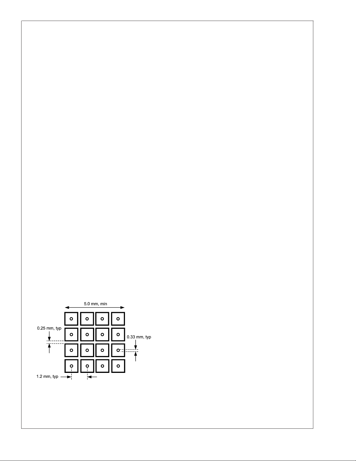
2.0 Applications Information
(Continued)
power down current because not all of the ADC is powered
down. The device current will be normal after the input clock
is established.
2.6.2 Thermal Management
The ADC08D1000 is capable of impressive speeds and
performance at very low power levels for its speed. However,
the power consumption is still high enough to require attention to thermal management. For reliability reasons, the die
temperature should be kept to a maximum of 130˚C. That is,
(ambient temperature) plus ADC power consumption
t
A
times θ
exceed 130˚C. This is not a problem if the ambient temperature is kept to a maximum of +85˚C with the requisite amount
of airflow as specified in the Operating Ratings section.
Please note that the following are general recommendations
for mounting exposed pad devices onto a PCB. This should
be considered the starting point in PCB and assembly process development. It is recommended that the process be
developed based upon past experience in package mounting.
The package of the ADC08D1000 has an exposed pad on its
back that provides the primary heat removal path as well as
excellent electrical grounding to the printed circuit board.
The land pattern design for lead attachment to the PCB
should be the same as for a conventional LQFP, but the
exposed pad must be attached to the board to remove the
maximum amount of heat from the package, as well as to
ensure best product parametric performance.
To maximize the removal of heat from the package, a thermal land pattern must be incorporated on the PC board
within the footprint of the package. The exposed pad of the
device must be soldered down to ensure adequate heat
conduction out of the package. The land pattern for this
exposed pad should be at least as large as the5x5mmof
the exposed pad of the package and be located such that the
exposed pad of the device is entirely over that thermal land
pattern. This thermal land pattern should be electrically connected to ground. A clearance of at least 0.5 mm should
separate this land pattern from the mounting pads for the
package pins.
Since a large aperture opening may result in poor release,
the aperture opening should be subdivided into an array of
smaller openings, similar to the land pattern of Figure 16.
(junction to ambient thermal resistance) should not
JA
20097421
FIGURE 16. Recommended Package Land Pattern
To minimize junction temperature, it is recommended that a
simple heat sink be built into the PCB. This is done by
including a copper area of about 2 square inches (6.5 square
cm) on the opposite side of the PCB. This copper area may
be plated or solder coated to prevent corrosion, but should
not have a conformal coating, which could provide some
thermal insulation. Thermal vias should be used to connect
these top and bottom copper areas. These thermal vias act
as "heat pipes" to carry the thermal energy from the device
side of the board to the opposite side of the board where it
can be more effectively dissipated. The use of 9 to 16
thermal vias is recommended.
The thermal vias should be placed on a 1.2 mm grid spacing
and have a diameter of 0.30 to 0.33 mm. These vias should
be barrel plated to avoid solder wicking into the vias during
the soldering process as this wicking could cause voids in
the solder between the package exposed pad and the thermal land on the PCB. Such voids could increase the thermal
resistance between the device and the thermal land on the
board, which would cause the device to run hotter.
If it is desired to monitor die temperature, a temperature
sensor may be mounted on the heat sink area of the board
near the thermal vias. .Allow for a thermal gradient between
the temperature sensor and the ADC08D1000 die of θ
times typical power consumption = 2.8 x 1.6 = 4.5˚C. Allowing for a 5.5˚C (including an extra 1˚C) temperature drop
from the die to the temperature sensor, then, would mean
that maintaining a maximum pad temperature reading of
124.5˚C will ensure that the die temperature does not exceed 130˚C, assuming that the exposed pad of the
ADC08D1000 is properly soldered down and the thermal
vias are adequate. (The inaccuracy of the temperature sensor is addtional to the above calculation).
2.7 LAYOUT AND GROUNDING
Proper grounding and proper routing of all signals are essential to ensure accurate conversion. A single ground plane
should be used, as apposed to splitting the ground plane into
analog and digital areas.
Since digital switching transients are composed largely of
high frequency components, the skin effect tells us that total
ground plane copper weight will have little effect upon the
logic-generated noise. Total surface area is more important
than is total ground plane volume. Coupling between the
typically noisy digital circuitry and the sensitive analog circuitry can lead to poor performance that may seem impossible to isolate and remedy. The solution is to keep the
analog circuitry well separated from the digital circuitry.
High power digital components should not be located on or
near any linear component or power supply trace or plane
that services analog or mixed signal components as the
resulting common return current path could cause fluctuation
in the analog input “ground” return of the ADC, causing
excessive noise in the conversion result.
Generally, we assume that analog and digital lines should
cross each other at 90˚ to avoid getting digital noise into the
analog path. In high frequency systems, however, avoid
crossing analog and digital lines altogether. The input clock
lines should be isolated from ALL other lines, analog AND
digital. The generally accepted 90˚ crossing should be
avoided as even a little coupling can cause problems at high
frequencies. Best performance at high frequencies is obtained with a straight signal path.
The analog input should be isolated from noisy signal traces
to avoid coupling of spurious signals into the input. This is
especially important with the low level drive required of the
ADC08D1000
Jc
www.national.com29
Page 30
2.0 Applications Information
(Continued)
ADC08D1000. Any external component (e.g., a filter capacitor) connected between the converter’s input and ground
ADC08D1000
should be connected to a very clean point in the analog
ground plane. All analog circuitry (input amplifiers, filters,
etc.) should be separated from any digital components.
this pin is floating, the output clock (DCLK) is a DDR (Double
Data Rate) clock (see Section 1.1.5.3) and the output edge
synchronization is irrelevant since data is clocked out on
both DCLK edges.
Pin 127, if it is high or low in the non-extended control mode,
sets the calibration delay. If pin 127 is floating, the calibration
delay is the same as it would be with this pin low and the
converter performs dual edge sampling (DES).
2.8 DYNAMIC PERFORMANCE
The ADC08D1000 is a.c. tested and its dynamic performance is guaranteed. To meet the published specifications
and avoid jitter-induced noise, the clock source driving the
CLK input must exhibit low rms jitter. The allowable jitter is a
function of the input frequency and the input signal level, as
described in Section 2.3.
It is good practice to keep the ADC input clock line as short
as possible, to keep it well away from any other signals and
to treat it as a transmission line. Other signals can introduce
jitter into the input clock signal. The clock signal can also
introduce noise into the analog path if not isolated from that
path.
Best dynamic performance is obtained when the exposed
pad at the back of the package has a good connection to
ground. This is because this path from the die to ground is a
lower impedance than offered by the package pins.
2.9 USING THE SERIAL INTERFACE
The ADC08D1000 may be operated in the non-extended
control (non-Serial Interface) mode or in the extended control mode. Table 6 and Table 7 describe the functions of pins
3, 4, 14 and 127 in the non-extended control mode and the
extended control mode, respectively.
2.9.1 Non-Extended Control Mode Operation
Non-extended control mode operation means that the Serial
Interface is not active and all controllable functions are controlled with various pin settings. That is, the full-scale range,
single-ended or differential input and input coupling (a.c. or
d.c.) are all controlled with pin settings. The non-extended
control mode is used by setting pin 14 high or low, as
opposed to letting it float. Table 6 indicates the pin functions
of the ADC08D1000 in the non-extended control mode.
TABLE 6. Non-Extended Control Mode Operation (Pin
14 High or Low)
Pin Low High Floating
0.44V
3
4
P-P
Output
OutEdge =
Neg
0.6V
P-P
Output
OutEdge =
Pos
n/a
DDR
127 CalDly Low CalDly High DES
14
650 mV
P-P
input range
860 mV
input range
P-P
Extended
Control
Mode
Pin 3 can be either high or low in the non-extended control
mode. Pin 14 must not be left floating to select this mode.
See Section 1.2 for more information.
Pin 4 can be high or low or can be left floating in the
non-extended control mode. In the non-extended control
mode, pin 4 high or low defines the edge at which the output
data transitions. See Section 2.4.3 for more information. If
TABLE 7. Extended Control Mode Operation (Pin 14
Floating)
Pin Function
3 SCLK (Serial Clock)
4 SDATA (Serial Data)
127 SCS (Serial Interface Chip Select)
2.10 COMMON APPLICATION PITFALLS Driving the inputs (analog or digital) beyond the power
supply rails. For device reliability, no input should go more
than 150 mV below the ground pins or 150 mV above the
supply pins. Exceeding these limits on even a transient basis
may not only cause faulty or erratic operation, but may
impair device reliability. It is not uncommon for high speed
digital circuits to exhibit undershoot that goes more than a
volt below ground. Controlling the impedance of high speed
lines and terminating these lines in their characteristic impedance should control overshoot.
Care should be taken not to overdrive the inputs of the
ADC08D1000. Such practice may lead to conversion inaccuracies and even to device damage.
Incorrect analog input common mode voltage in the d.c.
coupled mode. As discussed in section 1.3 and 3.0, the Input
common mode voltage must remain within 50 mV of the
output , which has a variability with temperature that
V
CMO
must also be tracked. Distortion performance will be degraded if the input common mode voltages more than 50 mV
CMO
.
from V
Using an inadequate amplifier to drive the analog input.
Use care when choosing a high frequency amplifier to drive
the ADC08D1000 as many high speed amplifiers will have
higher distortion than will the ADC08D1000, resulting in
overall system performance degradation.
Driving the V
pin to change the reference voltage. As
BG
mentioned in Section 2.1, the reference voltage is intended
to be fixed to provide one of two different full-scale values
(650 mV
and 860 mV
P-P
). Over driving this pin will not
P-P
change the full scale value, but can otherwise upset operation.
Driving the clock input with an excessively high level
signal. The ADC input clock level should not exceed the
level described in the Operating Ratings Table or the input
offset could change.
Inadequate input clock levels.As described in Section 2.3,
insufficient input clock levels can result in poor performance.
Excessive input clock levels could result in the introduction
of an input offset.
Using a clock source with excessive jitter, using an
excessively long input clock signal trace, or having
other signals coupled to the input clock signal trace.
This will cause the sampling interval to vary, causing excessive output noise and a reduction in SNR performance.
www.national.com 30
Page 31

2.0 Applications Information
(Continued)
Failure to provide adequate heat removal. As described in
Section 2.6.2, it is important to provide adequate heat re-
ADC08D1000
moval to ensure device reliability. This can either be done
with adequate air flow or the use of a simple heat sink built
into the board. The backside pad should be grounded for
best performance.
www.national.com31
Page 32

Physical Dimensions inches (millimeters) unless otherwise noted
NOTES: UNLESS OTHERWISE SPECIFIED
REFERENCE JEDEC REGISTRATION MS-026, VARIATION BFB.
128-Lead Exposed Pad LQFP
Order Number ADC08D1000CIYB
NS Package Number VNX128A
National does not assume any responsibility for use of any circuitry described, no circuit patent licenses are implied and National reserves
High Performance, Low Power, Dual 8-Bit, 1 GSPS A/D Converter
the right at any time without notice to change said circuitry and specifications.
For the most current product information visit us at www.national.com.
LIFE SUPPORT POLICY
NATIONAL’S PRODUCTS ARE NOT AUTHORIZED FOR USE AS CRITICAL COMPONENTS IN LIFE SUPPORT DEVICES OR SYSTEMS
WITHOUT THE EXPRESS WRITTEN APPROVAL OF THE PRESIDENT AND GENERAL COUNSEL OF NATIONAL SEMICONDUCTOR
CORPORATION. As used herein:
1. Life support devices or systems are devices or systems
which, (a) are intended for surgical implant into the body, or
(b) support or sustain life, and whose failure to perform when
properly used in accordance with instructions for use
2. A critical component is any component of a life support
device or system whose failure to perform can be reasonably
expected to cause the failure of the life support device or
system, or to affect its safety or effectiveness.
provided in the labeling, can be reasonably expected to result
in a significant injury to the user.
BANNED SUBSTANCE COMPLIANCE
National Semiconductor certifies that the products and packing materials meet the provisions of the Customer Products Stewardship
Specification (CSP-9-111C2) and the Banned Substances and Materials of Interest Specification (CSP-9-111S2) and contain no ‘‘Banned
Substances’’ as defined in CSP-9-111S2.
National Semiconductor
Americas Customer
Support Center
Email: new.feedback@nsc.com
Tel: 1-800-272-9959
www.national.com
National Semiconductor
Europe Customer Support Center
Fax: +49 (0) 180-530 85 86
Email: europe.support@nsc.com
Deutsch Tel: +49 (0) 69 9508 6208
English Tel: +44 (0) 870 24 0 2171
Français Tel: +33 (0) 1 41 91 8790
National Semiconductor
Asia Pacific Customer
Support Center
Email: ap.support@nsc.com
National Semiconductor
Japan Customer Support Center
Fax: 81-3-5639-7507
Email: jpn.feedback@nsc.com
Tel: 81-3-5639-7560
 Loading...