

Page 1
December 1998
ADC08831/ADC08832
8-Bit Serial I/O CMOS A/D Converters with Multiplexer
and Sample/Hold Function
General Description
The ADC08831/ADC08832 are 8-bit successive approximation Analog to Digital converters with 3-wire serial interfaces
and a configurable input multiplexer for 2 channels. The serial I/O will interface to COPS
sors, DSP’s, or shift registers. The serial I/O is configured to
comply with the NSC MICROWIRE
standard.
To minimize total power consumption, the
ADC08831/ADC08832 automatically go into low power
mode whenever they are not performing conversions.
Atrack/holdfunction allows the analog voltage at the positive
input to vary during the actual A/D conversion.
The analog inputs can be configured to operate in various
combination of single-ended, differential, or
pseudo-differential modes. The voltage reference input can
be adjusted to allow encoding of small analog voltage spans
to the full 8-bits of resolution.
™
family, PLD’s, microproces-
™
serial data exchange
Applications
n Digitizing sensors and waveforms
n Process control monitoring
n Remote sensing in noisy environments
n Instrumentation
n Embedded Systems
Features
n 3-wire serial digital data link requires few I/O pins
n Analog input track/hold function
n 2-channel input multiplexer option with address logic
n Analog input voltage range from GND to V
n No zero or full scale adjustment required
n TTL/CMOS input/output compatible
n Superior pin compatible replacement for ADC0831/2
CC
Key Specifications
n Resolution: 8 bits
n Conversion time (f
n Power dissipation: 8.5mW (typ)
n Low power mode 3.0mW (typ)
n Single supply: 5V
n Total unadjusted error:±1LSB
n No missing codes over temperature
=
2 MHz): 4µs (max)
C
DC
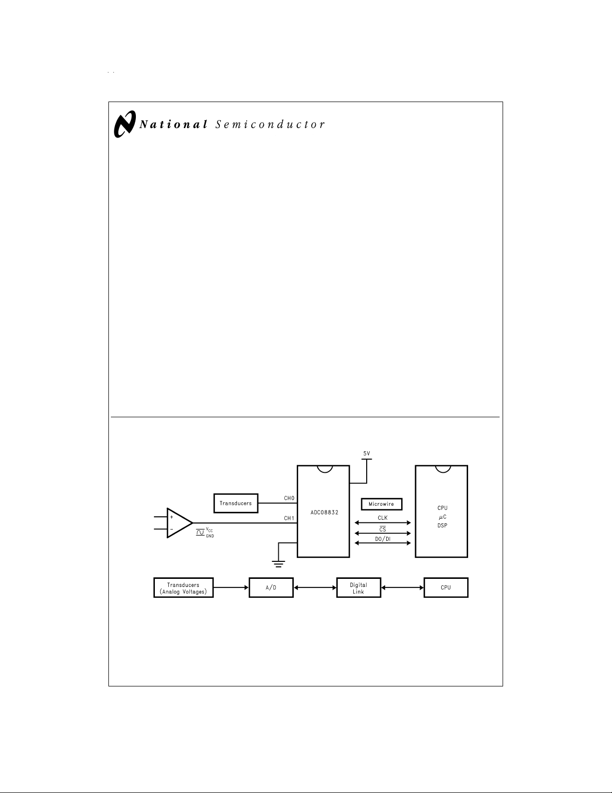
ADC08831/ADC08832 8-Bit Serial I/O CMOS A/D Converters with Multiplexer and Sample/Hold
Function
Typical Application
DS100108-44
DS100108-43
COPS™is a trademark of National Semiconductor Corporation.
™
MICROWIRE
TRI-STATE
© 1998 National Semiconductor Corporation DS100108 www.national.com
is a trademark of National Semiconductor Corporation.
™
Page 2
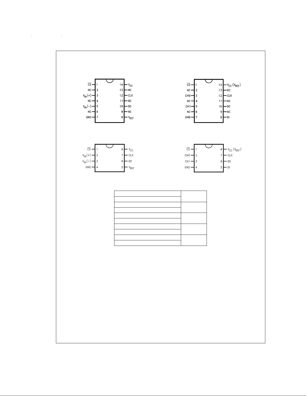
Connection Diagrams
ADC08831
Wide Body SO Packages
ADC08831
N,M,MM Packages
Ordering Information
DS100108-4
DS100108-2
Temperature Range Package
Industrial (−40˚C ≤ T
≤ +85˚C)
J
ADC08831IN
ADC08832IN
ADC08831IWM,
ADC08832IWM,
ADC08831IM,
ADC08832IM,
ADC08831IMM,
ADC08832IMM,
ADC08832
Wide Body SO Packages
DS100108-3
ADC08832
N,M,MM Packages
DS100108-1
N08E
M14B
M08A
MUA08A
www.national.com 2
Page 3
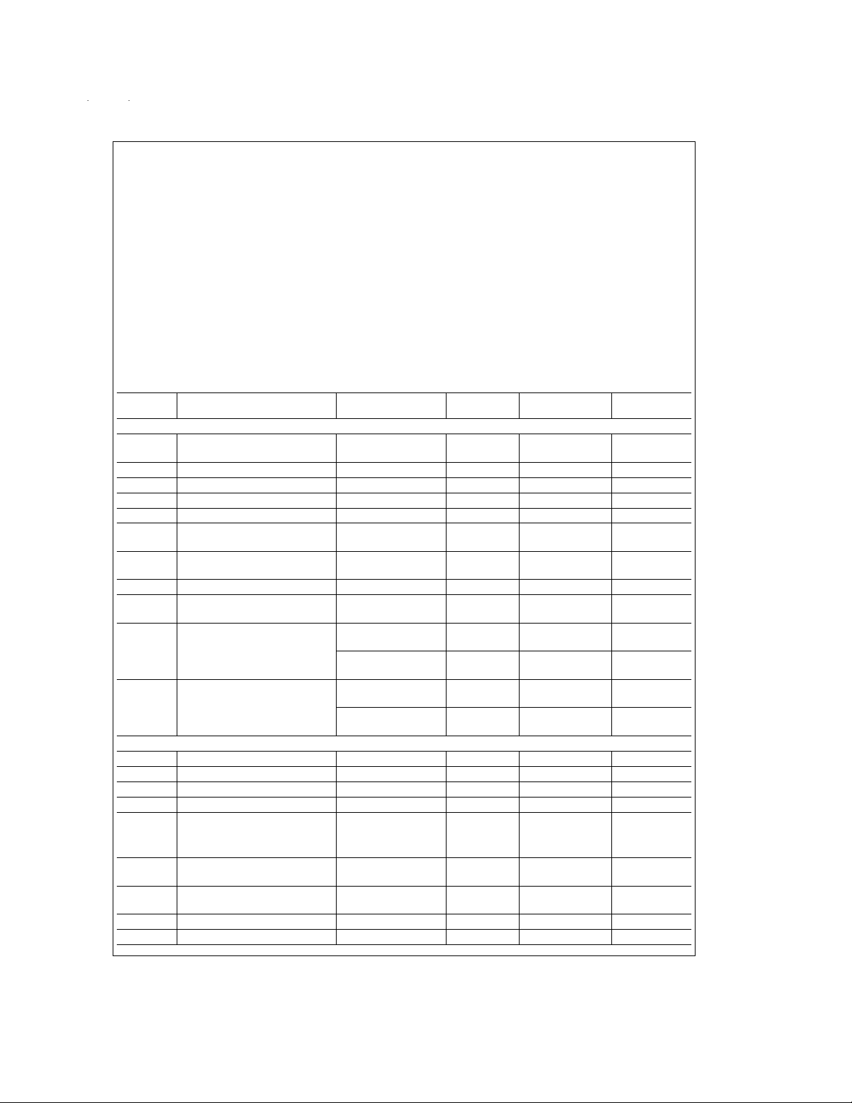
Absolute Maximum Ratings (Notes 1, 3)
If Military/Aerospace specified devices are required,
please contact the National Semiconductor Sales Office/
Distributors for availability and specifications.
Supply Voltage (V
Voltage at Inputs and Outputs −0.3V to V
Input Current at Any Pin (Note 4)
Package Input Current (Note 4)
ESD Susceptibility (Note 6)
Human Body Model 2000V
Machine Model 200V
Junction Temperature(Note 5) 150˚C
Storage Temperature Range −65˚ C to 150˚C
) 6.5V
CC
CC
±
+ 0.3V
±
5mA
20 mA
Mounting Temperature
Lead Temp. (soldering, 10 sec)
Infrared (10 sec)
260˚C
215˚C
Operating Ratings(Notes 2, 3)
Temperature Range −40˚C ≤ T
Supply Voltage 4.5 V to 6.0 V
Thermal Resistance (θ
)
jA
SO Package, 8-pin Surface Mount 190˚C/W
MSOP, 8-pin Surface Mount 235˚C/W
SO Package, 14-pin Surface Mount 145˚C/W
N Package, 8-pin 122˚C/W
Clock Frequency 10kHz≤f
≤ +85˚C
J
CLK
≤2MHz
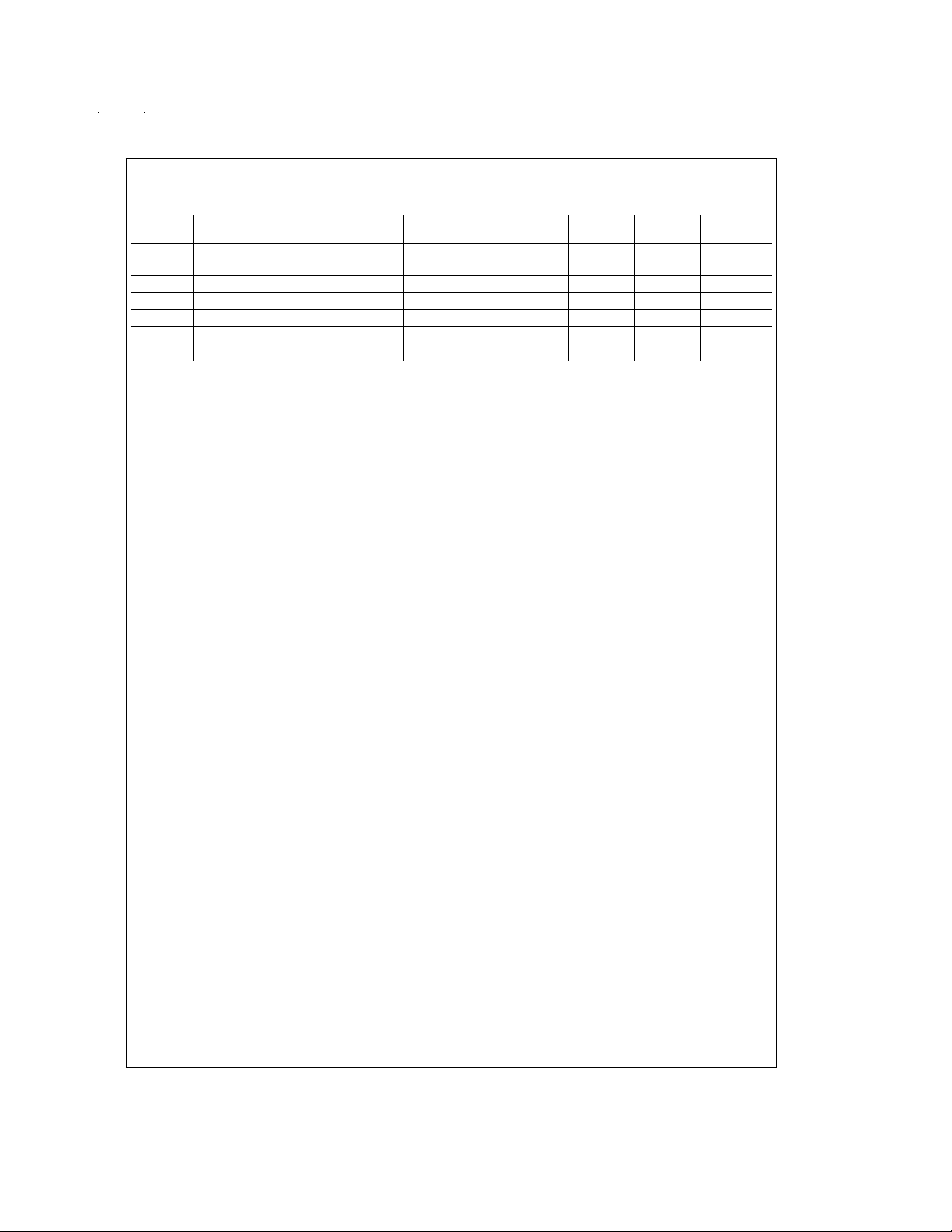
Electrical Characteristics
=
The following specifications apply for V
apply for T
=
=
to T
T
A
T
J
MIN
; all other limits T
MAX
CC
=
+5V
A
, and f
DC
=
=
T
J
V
REF
Symbol Parameter Conditions Typical
CONVERTER AND MULTIPLEXER CHARACTERISTICS
TUE Total Unadjusted Error (Note 10)
Offset Error
DNL Differential NonLinearity
INL Integral NonLinearity
FS Full Scale Error
R
REF
V
IN
Reference Input Resistance (Note 11) 3.5 2.8
Analog Input Voltage (Note 12) (VCC+ 0.05)
DC Common-Mode Error
Power Supply Sensitivity V
On Channel Leakage Current
(Note 13)
=
5V
CC
=
5V
V
CC
On Channel=5V,
Off Channel=0V
On Channel=0V
Off Channel=5V
Off Channel Leakage Current
(Note 13)
On Channel=5V,
Off Channel=0V
On Channel=0V,
Off Channel=5V
DC CHARACTERISTICS
V
IN(1)
V
IN(0)
I
IN(1)
I
IN(0)
V
OUT(1)
V
OUT(0)
I
OUT
I
SOURCE
I
SINK
Logical “1” Input Voltage 2.0 V (min)
Logical “0” Input Voltage 0.8 V (max)
Logical “1” Input Current V
Logical “0” Input Current V
Logical “1” Output Voltage V
Logical “0” Output Voltage V
TRI-STATE Output Current V
Output Source Current V
Output Sink Current V
=
5.0V 0.05 +1 µA (max)
IN
=
0V 0.05 −1 µA (max)
IN
=
4.75V:
CC
=
I
−360 µA 2.4 V (min)
OUT
=
I
−10 µA 4.5 V (min)
OUT
=
4.75V
CC
=
1.6 mA
I
OUT
=
0V
OUT
=
5V
V
OUT
=
0V −6.5 mA (max)
OUT
=
V
OUT
CC
25˚C.
±
10%,
±
5
=
2 MHz unless otherwise specified. Boldface limits
CLK
(Note 8)
±
±
±
±
±
%
0.3
Limits
(Note 9)
±
1 LSB
Units
(Limits)
(max)
0.2 LSB
0.2 LSB
0.2 LSB
0.3 LSB
kΩ (min)
5.9
kΩ (max)
V (max)
(GND − 0.05)
1
±
⁄
4
1
±
⁄
4
1
±
⁄
4
0.2
V (min)
LSB (max)
LSB (max)
LSB (max)
µA (max)
1
−0.2
µA (min)
−1
−0.2
µA (min)
−1
0.2
µA (max)
1
0.4 V (max)
−3.0
3.0
µA (max)
µA (max)
8.0 mA (min)
www.national.com3
Page 4
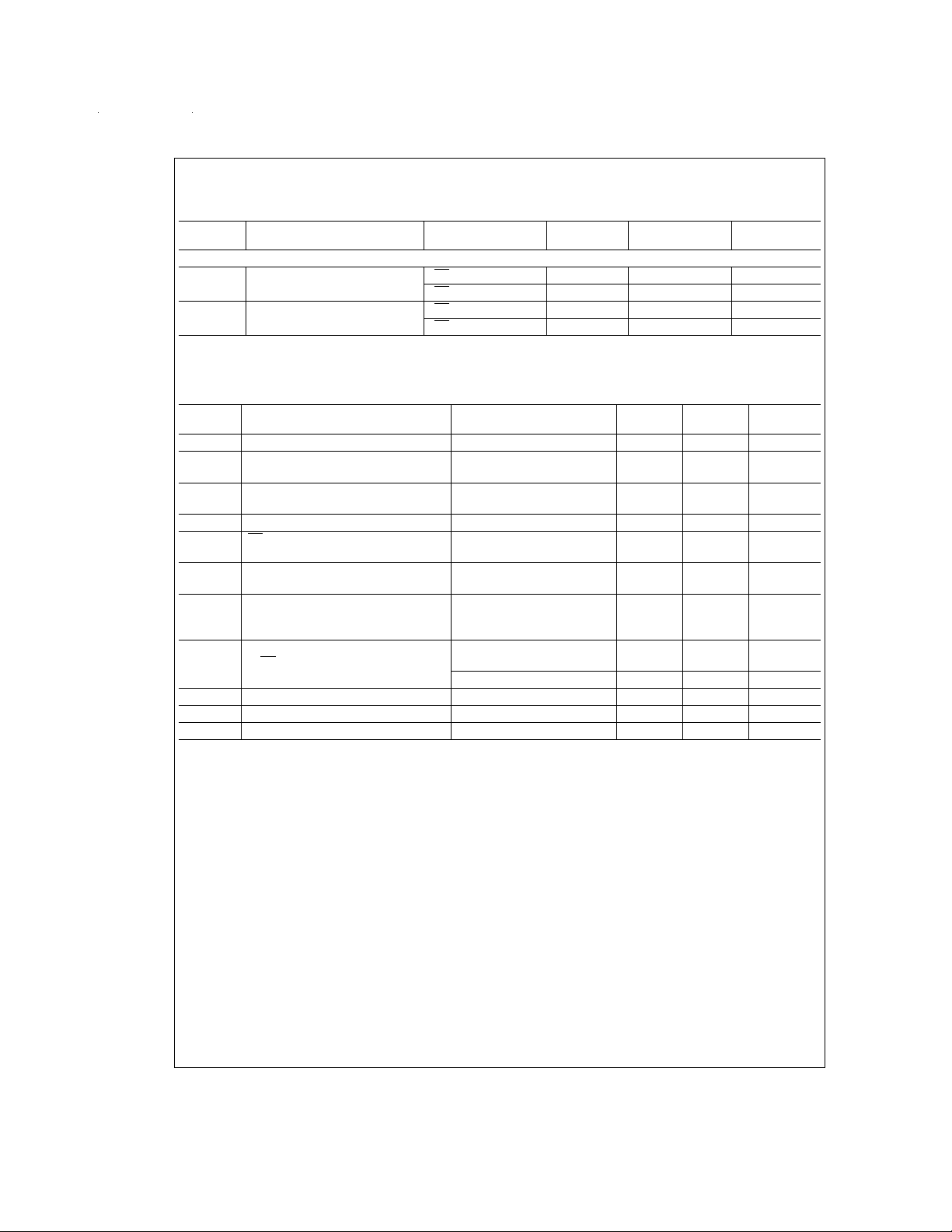
Electrical Characteristics (Continued)
=
The following specifications apply for V
apply for T
=
=
to T
T
A
T
J
MIN
; all other limits T
MAX
CC
=
+5V
A
, and f
DC
=
=
T
J
V
REF
Symbol Parameter Conditions Typical
DC CHARACTERISTICS
I
CC
I
CC
Supply Current ADC08831
CLK=high
Supply Current ADC08832
CLK=high (Note 16)
CS=V
CC
CS=LOW
CS=V
CC
CS=LOW
25˚C.
=
2 MHz unless otherwise specified. Boldface limits
CLK
(Note 8)
0.6 1.0 mA (max)
1.7 2.4 mA (max)
1.3 1.8 mA (max)
2.4 3.5 mA (max)
Limits
(Note 9)
Units
(Limits)
Electrical Characteristics
=
The following specifications apply for V
apply for T
=
=
to T
T
A
T
J
MIN
; all other limits T
MAX
CC
=
V
+5 V
REF
DC
=
T
A
J
Symbol Parameter Conditions Typical
f
CLK
Clock Frequency 2 MHz (max)
Clock Duty Cycle
(Note 14)
T
C
t
CA
t
SET-UP
t
HOLD
t
pd1,tpd0
Conversion Time (Not Including MUX
Addressing Time)
Acquisition Time
CS Falling Edge or Data Input
Valid to CLK Rising Edge
Data Input Valid after CLK
Rising Edge
CLK Falling Edge to Output
Data Valid (Note 15)
f
CLK
C
L
Data MSB First
Data LSB First
t
1H,t0H
C
IN
C
IN
C
OUT
TRI-STATE Delay from Rising Edge
of CS to Data Output and SARS Hi-Z
Capacitance of Analog input (Note 17) 13 pF
Capacitance of Logic Inputs 5 pF
Capacitance of Logic Outputs 5 pF
C
L
(see TRI-STATE Test Circuits)
C
L
=
, and t
=
25˚C.
=
t
20 ns unless otherwise specified. Boldface limits
r
f
(Note 8)
=
2MHz 8
=
100 pF:
=
10 pF, R
=
100 pF, R
=
10 kΩ
L
=
2kΩ 180 ns (max)
L
50 ns
Limits
(Note 9)
40
60
1/f
4
1
⁄
2
1/f
25 ns (min)
20 ns (min)
250
200
Units
(Limits)
%
(min)
%
(max)
(max)
CLK
µs (max)
(max)
CLK
ns (max)
ns (max)
www.national.com 4
Page 5
Dynamic Characteristics
The following specifications apply for V
5V, non-coherent 2048 samples with windowing.
=
CC
Symbol Parameter Conditions Typical
f
S
Sampling Rate ADC08831
ADC08832
SNR Signal-to -Noise Ratio (Note 19) 48.5 dB
THD Total Harmonic Distortion (Note 20) −59.5 dB
SINAD Signal-to -Noise and Distortion 48.0 dB
ENOB Effective Number Of Bits (Note 18) 7.7 Bits
SFDR Spurious Free Dynamic Range 62.5 dB
Note 1: Absolute Maximum Ratings indicate limits beyond which damage to the device may occur.
Note 2: Operating Ratings indicate conditions for which the device is functional. These ratings do not guarantee specific performance limits. For guaranteed speci-
fications and test conditions, see the Electrical Characteristics. The guaranteed specifications apply only for the test conditions listed. Some performance characteristics may degrade when the device is not operated under the listed test conditions.
Note 3: All voltages are measured with respect to GND=0V
Note 4: When the input voltage V
mA maximum package input current rating limits the number of pins that can safely exceed the power supplies with an input current of 5 mA to four pins.
Note 5: The maximum power dissipation must be derated at elevated temperatures and is dictated by T
allowable power dissipation at any temperature is P
Note 6: Human body model, 100 pF capacitor discharged through a 1.5 kΩ resistor. The machine mode is a 200pF capacitor discharged directly into each pin.
Note 7: SeeAN450 “Surface Mounting Methods and Their Effect on Product Reliability” or Linear Data Book section “Surface Mount” for other methods of soldering
surface mount devices.
Note 8: Typicals are at T
Note 9: Guaranteed to National’s AOQL (Average Outgoing Quality Level).
Note 10: Total unadjusted error includes offset, full-scale, linearity, multiplexer errors.
Note 11: It is not tested for the ADC08832.
Note 12: For V
forward-conduct for analog input voltages one diode drop below ground or one diode drop greater than V
level analog inputs (e.g., 5V) can cause an input diode to conduct, especially at elevated temperatures, which will cause errors for analog inputs near full-scale. The
spec allows 50 mV forward bias of either diode; this means that as long as the analog V
will be correct. Exceeding this range on an unselected channel will corrupt the reading of a selected channel. Achievement of an absolute 0 V
range will therefore require a minimum supply voltage of 4.950 V
Note 13: Channel leakage current is measured after a single-ended channel is selected and the clock is turned off. For off channel leakage current the following two
cases are considered: one, with the selected channel tied high (5 V
measured; two, with the selected channel tied low and the off channels tied high, total current flow through the off channel is again measured. The two cases considered for determining on channel leakage current are the same except total current flow through the selected channel is measured.
Note 14: A40%to 60%duty cycle range insures proper operation at all clock frequencies. In the case that an available clock has a duty cycle outside of these limits
the minimum time the clock is high or low must be at least 250 ns. The maximum time the clock can be high or low is 60 µs.
Note 15: Since data, MSB first, is the output of the comparator used in the successive approximation loop, an additional delay is built in to allow for comparator response time.
Note 16: For the ADC08832 V
Note 17: Analog inputs are typically 300 ohms input resistance to a 13pF sample and hold.
Note 18: Effective Number Of Bits (ENOB) is calculated from the measured signal-to-noise plus distortion ratio (SINAD) using the equation ENOB=(SINAD-1.76)/
6.02.
Note 19: The signal-to-noise ratio is the ratio of the signal amplitude to the background noise level. Harmonics of the input signal are not included in it’s calculation.
Note 20: The contributions from the first 6 harmonics are used in the calculation of the THD.
IN(−)
≥ V
at any pin exceeds the power supplies (V
IN
=
D
=
25˚C and represent the most likely parametric norm.
J
the digital code will be 0000 0000. Two on-chip diodes are tied to each analog input (see Functional Block Diagram) which will
IN(+)
is internally tied to VCC, therefore, for the ADC08832 reference current is included in the supply current.
ref
=
5V, f
(T
2MHz, T
CLK
f
CLK
f
CLK
, unless otherwise specified.
DC
)/θJAor the number given in the Absolute Maximum Ratings, whichever is lower.
JMAX−TA
over temperature variations, initial tolerance and loading.
DC
) and the remaining off channel tied low (0 VDC), total current flow through the off channel is
DC
/11
/13
=
A
25˚C, R
SOURCE
=
50Ω,f
=
IN
(Note 8)
45kHz, V
IN
Limits
(Note 9)
181
153
<
IN
(GND) or V
>
VCC,) the current at that pin should be limited to 5 mA. The 20
IN
, θJAand the ambient temperature, TA. The maximum
JMAX
supply.During testing at low VCClevels (e.g., 4.5V), high
CC
does not exceed the supply voltage by more than 50 mV, the output code
IN
=
5V
P-P,VREF
(Limits)
to5VDCinput voltage
DC
Units
ksps
ksps
=
www.national.com5
Page 6
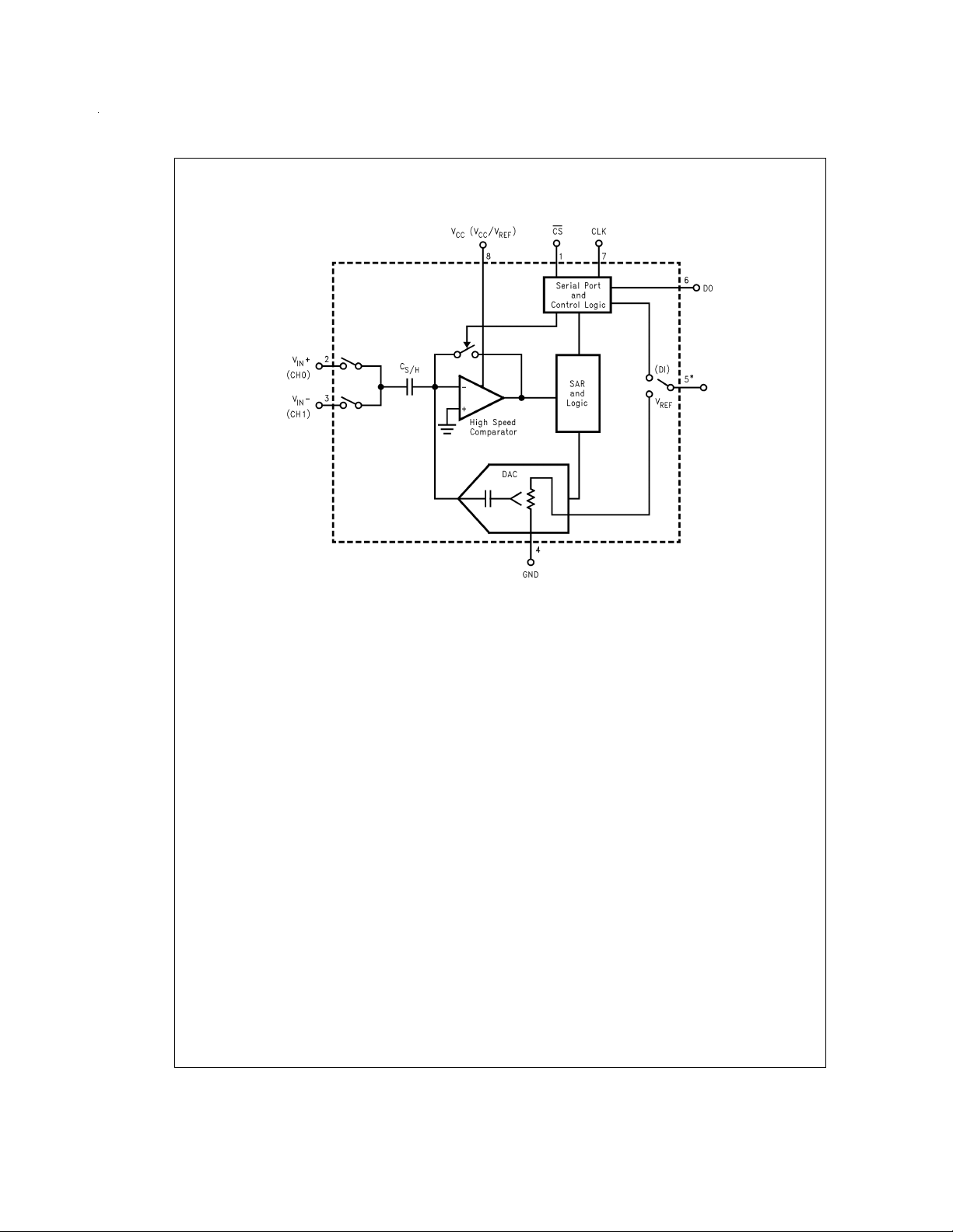
Block Diagram
*
For ADC08831 V
Pin names in parentheses refer to ADC08832
pin is available, for ADC08832 DI pin is available, and V
REF
REF
is tied to V
DS100108-47
CC
www.national.com 6
Page 7
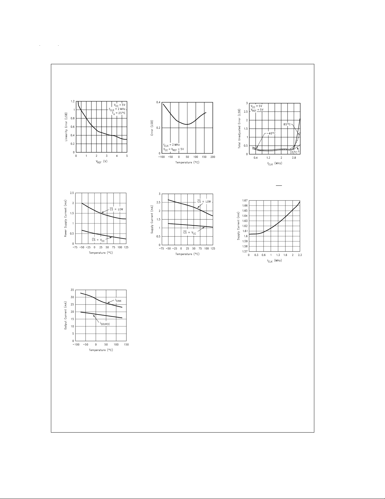
Typical Performance Characteristics The following specifications apply for T
5V, unless otherwise specified.
A
=
25˚C, V
=
=
V
CC
REF
Linearity Error (TUE) vs
Reference Voltage
Power Supply Current vs
Temperature (ADC08831)
DS100108-27
DS100108-35
Linearity Error (TUE) vs
Temperature
Power Supply Current vs
Temperature (ADC08832)
DS100108-15
DS100108-36
Linearity Error (TUE) vs
Clock Frequency
DS100108-14
Power Supply Current
vs Clock Frequency, CS=Low,
ADC08831
DS100108-37
Output Current vs
Temperature
DS100108-33
www.national.com7
Page 8
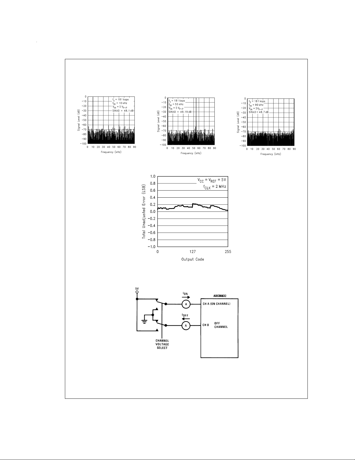
Typical Performance Characteristics The following specifications apply for T
5V, unless otherwise specified. (Continued)
A
=
25˚C, V
=
=
V
CC
REF
Spectral Response with 10KHz
Sine Wave Input
DS100108-13
Total Unadjuster Error Plot
Spectral Response with 55 KHz
Sine Wave Input
DS100108-34
Spectral Response with 90 KHz
Sine Wave Input
DS100108-16
Leakage Current Test Circuit
www.national.com 8
DS100108-38
DS100108-5
Page 9

TRI-STATE Test Circuits and Waveforms
Timing Diagrams
DS100108-20
DS100108-21
Data Input Timing
DS100108-22
Data Output Timing
DS100108-23
www.national.com9
Page 10

Timing Diagrams (Continued)
ADC08831 Start Conversion Timing
DS100108-24
ADC08831 Timing
*LSB first output not available on ADC08831.
ADC08832 Timing
www.national.com 10
DS100108-25
DS100108-26
Page 11

ADC08832 Functional Block Diagram
DS100108-12
*Some of these functions/pins are not available with other options.
www.national.com11
Page 12

Functional Description
1.0 MULTIPLEXER ADDRESSING
The design of these converters utilizes a comparator structure with built-in sample-and-hold which provides for a differential analog input to be converted by a successive approximation routine.
The actual voltage converted is always the difference between an assigned “+” input terminal and a “−” input terminal.
The polarity of each input terminal of the pair indicates which
line the converter expects to be the most positive. If the assigned “+” input voltage is less than the “−” input voltage the
converter responds with an all zeros output code.
A unique input multiplexing scheme has been utilized to provide multiple analog channels with software-configurable
single-ended, or differential operation. The analog signal
conditioning required in transducer-based data acquisition
systems is significantly simplified with this type of input flexibility. One converter package can now handle ground referenced inputs, differential inputs, as well as signals with some
arbitrary reference voltage.
A particular input configuration is assigned during the MUX
addressing sequence, prior to the start of a conversion. The
MUX address selects which of the analog inputs are to be
enabled and whether this input is single-ended or differential.
In addition to selecting differential mode the polarity may
also be selected. Channel 0 may be selected as the positive
input and channel 1 as the negative input or vice versa. This
programmability is illustrated by the MUX addressing codes
for the ADC08832.
The MUX address is shifted into the converter via the DI line.
Because the ADC08831 contains only one differential input
channel with a fixed polarity assignment, it does not require
addressing.
TABLE 1. Multiplexer/Package Options
Part
Number
ADC08831 1 1 8 or 14
ADC08832 2 1 8 or 14
Number of Analog
Channels
Single-Ended Differential
Number of
Package
Pins
MUX Addressing:
ADC08832
Single-Ended MUX Mode
MUX Address Channel
Start
SGL/
DIF
SGL/
DIF
ODD/
SIGN
ODD/
SIGN
Bit
110+
111 +
Differential MUX Mode
MUX Address Channel
Start
Bit
100+−
101−+
#
01
#
01
Since the input configuration is under software control, it can
be modified as required before each conversion. A channel
can be treated as a single-ended, ground referenced input
for one conversion; then it can be reconfigured as part of a
differential channel for another conversion.
The analog input voltages for each channel can range from
50mV below ground to 50mV above V
out degrading conversion accuracy.
2.0 THE DIGITAL INTERFACE
A most important characteristic of these converters is their
serial data link with the controlling processor. Using a serial
communication format offers two very significant system improvements. It allows many functions to be included in a
small package and it can eliminate the transmission of low
level analog signals by locating the converter right at the
analog sensor; transmitting highly noise immune digital data
back to the host processor.
To understand the operation of these converters it is best to
refer to the Timing Diagrams and Functional Block Diagram
and to follow a complete conversion sequence. For clarity, a
separate timing diagram is shown for each device.
1. A conversion is initiated by pulling the CS (chip select)
line low.This line must be held low for the entire conversion. The converter is now waiting for a start bit and its
MUX assignment word, if applicable.
2. Oneach rising edge of the clock the status of the data in
(DI) line is clocked into the MUX address shift register.
The start bit is the first logic “1” that appears on this line
(all leading zeros are ignored). Following the start bit the
converter expects the next 2 bits to be the MUX assignment word.
3. Whenthe start bit has been shifted into the start location
of the MUX register, and the input channel has been assigned, a conversion is about to begin. An interval of
clock period (where nothing happens) is automatically
inserted to allow the selected MUX channel to settle to a
final analog input value. The DI line is disabled at this
time. It no longer accepts data.
4. The data out (DO) line now comes out of TRI-STATE
and provides a leading zero for this one clock period of
MUX settling time.
5. Duringthe conversion the output of the SAR comparator
indicates whether the analog input is greater than (high)
or less than (low) a series of successive voltages generated internally from a ratioed capacitor array (first 5 bits)
and a resistor ladder (last 3 bits). After each comparison
the comparator’s output is shipped to the DO line on the
falling edge of CLK. This data is the result of the conversion being shifted out (with the MSB first) and can be
read by the processor immediately.
6. After 8 clock periods the conversion is completed.
7. Thestored data in the successive approximation register
is loaded into an internal shift register. The data, LSB
first, is automatically shifted out the DO line after the
MSB first data stream. The DO line then goes low and
stays low until CS is returned high. The ADC08831 is an
exception in that its data is only output in MSB first format.
8. TheDI and DO lines can be tied together and controlled
through a bidirectional processor I/O bit with one wire.
This is possible because the DI input is only “looked-at”
during the MUX addressing interval while the DO line is
still in a high impedance state.
(typically 5V) with-
CC
1
⁄
2
www.national.com 12
Page 13

Functional Description (Continued)
3.0 Reducing Power Consumption
The ADC08831 operate up to a 2MHz clock frequency, or
about 181 ksps. At 5V supply, it consumes about 1.7 mA or
8.5 mW when CS is logic low. The ADC08831 has a low
power mode to minimize total power consumption.
When the chip select is asserted with a logic high, some analog circuitry and digital logic are pulled to a static, low power
condition. Also, DOUT, the output driver is taken into
TRI-STATE mode.
To optimize static power consumption, special attention is
needed to the digital input logic signals: CLK, CS, DI. Each
digital input has a large CMOS buffer between VCCand
GND. A traditional TTL level high (2.4V) will be sufficient for
each input to read a logical “1”. However, there could be a
large V
voltage difference would cause static power dissipation,
even when chip select pin is high and the part is in low power
mode.
Therefore, to minimize static power dissipation, it is recommended that all digital input logic levels should equal the
converter’s supply. Various CMOS logic is particularly well
suited for this application.
The reference pin on the ADC08831 is not affected by the
power-down mode. To reduce static reference current during
non-conversion time, there are a couple options. First, a low
voltage external reference (ie, 2.5V could be used). A shunt
reference, such as the LM385-2.5, could be powered by a
logic gate that is the inverse of the signal on CS . When CS
is high, the reference is off. As a second option, an external,
low on-resistance switch could be used.
The ADC08832 is similar to the ADC08831, except its reference is derived from V
low-power mode when CS is logic high, as the analog and
to VCCvoltage difference at each input. Such a
IH
. The ADC08832 does enter a
CC
digital logic enter static current modes. However power dissipation from the reference ladder occurs, regardless of the
signal on CS
4.0 REFERENCE CONSIDERATIONS
The voltage applied to the reference input on these converters, V
, defines the voltage span of the analog input (the
REF
difference between V
possible output codes apply.The devices can be used either
IN(MAX)
and V
over which the 256
IN(MIN)
in ratiometric applications or in systems requiring absolute
accuracy.The reference pin must be connected to a voltage
source capable of driving the reference input resistance
which can be as low as 2.8kΩ. This pin is the top of a resistor
divider string and capacitor array used for the successive approximation conversion.
In a ratiometric system the analog input voltage is proportional to the voltage used for the A/D reference. This voltage
is typically the system power supply, so the V
tied to V
nique relaxes the stability requirements of the system refer-
(done internally on the ADC08832). This tech-
CC
REF
pin can be
ence as the analog input and A/D reference move together
maintaining the same output code for a given input condition.
For absolute accuracy, where the analog input varies between very specific voltage limits, the reference pin can be
biased with a time and temperature stable voltage source.
The LM385, LM336 and LM4040 reference diodes are good
low current devices to use with these converters.
The maximum value of the reference is limited to the V
supply voltage. The minimum value, however, can be quite
small (see Typical Performance Characteristics) to allow direct conversions of transducer outputs providing less than a
5V output span. Particular care must be taken with regard to
noise pickup, circuit layout and system error voltage sources
when operating with a reduced span due to the increased
sensitivity of the converter (1 LSB equals V
REF/
256).
CC
a) Ratiometric
DS100108-28
FIGURE 1. Reference Examples
b) Absolute with a Reduced Span
DS100108-29
www.national.com13
Page 14

Functional Description (Continued)
5.0 THE ANALOG INPUTS
The most important feature of these converters is that they
can be located right at the analog signal source and through
just a few wires can communicate with a controlling processor with a highly noise immune serial bit stream. This in itself
greatly minimizes circuitry to maintain analog signal accuracy which otherwise is most susceptible to noise pickup.
However, a few words are in order with regard to the analog
inputs should the input be noisy to begin with or possibly
riding on a large common-mode voltage.
The differential input of these converters actually reduces
the effects of common-mode input noise, a signal common
to both selected “+” and “−” inputs for a conversion (60 Hz is
most typical). The time interval between sampling the “+” input and then the “−” input is
in the common-mode voltage during this short time interval
can cause conversion errors. For a sinusoidal
common-mode signal this error is:
where fCMis the frequency of the common-mode signal,
is its peak voltage value
V
PEAK
is the A/D clock frequency.
and f
CLK
For a 60Hz common-mode signal to generate a
()5mV) with the converter running at 250kHz, its peak value
would have to be 6.63V which would be larger than allowed
as it exceeds the maximum analog input limits.
Source resistance limitation is important with regard to the
DC leakage currents of the input multiplexer.Bypass capacitors should not be used if the source resistance is greater
than 1kΩ. The worst-case leakage current of
perature will create a 1mV input error with a 1kΩ source resistance. An op amp RC active low pass filter can provide
both impedance buffering and noise filtering should a high
impedance signal source be required.
5.1 Sample and Hold
The ADC08831/2 provide a built-in sample-and-hold to acquire the input signal. The sample and hold can sample input
signals in either single-ended or pseudo differential mode.
5.2 Input Op Amps
When driving the analog inputs with an op amp it is important
that the op amp settle within the allowed time. Toachieve the
full sampling rate, the analog input should be driven with a
low impedance source (100Ω) or a high-speed op amp such
as the LM6142. Higher impedance sources or slower op
amps can easily be accommodated by allowing more time
for the analog input to settle.
5.3 Source Resistance
The analog inputs of the ADC08831/2 look like a 13pF capacitor (C
switched between the selected “+” and “−” inputs during
) in series with 300Ω resistor (Ron). CINgets
IN
each conversion cycle. Large external source resistors will
slow the settling of the inputs. It is important that the overall
RC time constants be short enough to allow the analog input
to completely settle.
1
⁄2of a clock period. The change
1
⁄4LSB error
±
1µAover tem-
5.4 Board layout Consideration, grounding and
bypassing:
The ADC08831/2 are easy to use with some board layout
consideration. They should be used with an analog ground
plane and single-point grounding techniques. The GND pin
should be tied directly to the ground plane.
The supply pin should be bypassed to the ground plane with
a surface mount or ceramic capacitor with leads as short as
possible. All analog inputs should be referenced directly to
the single-point ground. Digital inputs and outputs should be
shielded from and routed away from the reference and analog circuitry.
6.0 OPTIONAL ADJUSTMENTS
6.1 Zero Error
The offset of theA/D does not require adjustment. If the minimum analog input voltage value, V
zero offset can be done. The converter can be made to out-
, is not ground a
IN(MIN)
put 0000 0000 digital code for this minimum input voltage by
biasing any V
the differential mode operation of the A/D.
(−) input at this V
IN
value. This utilizes
IN(MIN)
The zero error of the A/D converter relates to the location of
the first riser of the transfer function and can be measured by
grounding the V
positive voltage to the V
ence between the actual DC input voltage which is necessary to just cause an output digital code transition from 0000
0000 to 0000 0001 and the ideal
9.8mV for V
(−) input and applying a small magnitude
REF
IN
=
(+) input. Zero error is the differ-
IN
1
⁄2LSB value (1⁄2LSB
5.000V
).
DC
6.2 Full Scale
The full-scale adjustment can be made by applying a differential input voltage which is 1
1
⁄2LSB down from the desired
analog full-scale voltage range and then adjusting the magnitude of the V
tal output code which is just changing from 1111 1110 to 1111
input (or VCCfor the ADC08832) for a digi-
REF
1111.
6.3 Adjusting for an Arbitrary Analog Input
Voltage Range
If the analog zero voltage of the A/D is shifted away from
ground (for example, to accommodate an analog input signal
which does not go to ground), this new zero reference
should be properly adjusted first. A V
equals this desired zero reference plus
(+) voltage which
IN
1
⁄2LSB (where the
LSB is calculated for the desired analog span, using 1 LSB
analog span/256) is applied to selected “+” input and the
zero reference voltage at the corresponding “−” input should
then be adjusted to just obtain the 00
sition.
HEX
to 01
HEX
code tran-
The full-scale adjustment should be made [with the proper
V
(−) voltage applied] by forcing a voltage to the VIN(+) in-
IN
put which is given by:
where:
=
V
the high end of the analog input range
MAX
and
=
the low end (the offset zero) of the analog range.
V
MIN
(Both are ground referenced.)
=
=
www.national.com 14
Page 15

Functional Description (Continued)
The V
IN (or VCC) voltage is then adjusted to provide a
REF
code change from FE
justment procedure.
7.0 DYNAMIC PERFORMANCE
Dynamic performance specifications are often useful in applications requiring waveform sampling and digitization.
Typically, a memory buffer is used to capture a stream of
consecutive digital outputs for post processing. Capturing a
number of samples that is a power of 2 (ie, 1024, 2048,
4096) allows the Fast Fourier Transform (FFT) to be used to
digitally analyze the frequency components of the signal.
Depending on the application, further digital filtering, windowing, or processing can be applied.
7.1 Sampling Rate
The Sampling Rate, sometimes referred to as the Throughput Rate, is the time between repetitive samples by an
Analog-to-Digital Converter. The sampling rate includes the
conversion time, as well as other factors such a MUX setup
time, acquisition time, and interfacing time delays. Typically,
the sampling rate is specified in the number of samples
taken per second, at the maximum Analog-to-Digital Converter clock frequency.
Signals with frequencies exceeding the Nyquist frequency
(1/2 the sampling rate), will be aliased into frequencies below the Nyquist frequency. To prevent signal degradation,
sample at twice (or more) than the input signal and/or use of
a low pass (anti-aliasing) filter on the front-end. Sampling at
a much higher rate than the input signal will reduce the requirements of the anti-aliasing filter.
Some applications require under-sampling the input signal.
In this case, one expects the fundamental to be aliased into
the frequency range below the Nyquist frequency. In order to
be assured the frequency response accurately represents a
harmonic of the fundamental, a band-pass filter should be
used over the input range of interest.
7.2 Signal-to-Noise Ratio
Signal-to-Noise Ratio (SNR) is the ratio of RMS magnitude
of the fundamental to the RMS sum of all the
non-fundamental signal, excluding the harmonics, up to 1/2
of the sampling frequency (Nyquist).
7.3 Total Harmonic Distortion
Total Harmonic distortion is the ratio of the RMS sum of the
amplitude of the harmonics to the fundamental input frequency.
THD=20 log [(V
Where V
V
harmonics. In theory, all harmonics are included in THD cal-
is the RMS amplitude of the fundamental and
1
2,V3,V4,V5,V6
culations, but in practice only about the first 6 make significant contributions and require measurement.
For under-sampling applications, the input signal should be
band pass filtered (BPF) to prevent out of band signals, or
their harmonics, to appear in the spectral response.
The DC Linearity transfer function of an Analog-to-Digital
Converter tends to influence the dominant harmonics. A
parabolic Linearity curve would tend to create 2
order harmonics, while an S-curve would tend to create 3
(or odd) order harmonics. The magnitude of an DC linearity
error correlates to the magnitude of the harmonics.
to FF
HEX
2
+V
2
. This completes the ad-
HEX
2
2
4
+V
2
5
+V
3
+V
1/2
2
)
/V1]
6
are the RMS amplitudes of the individual
nd
(and even)
7.4 Signal-to-Noise And Distortion
Signal-to-Noise And Distortion ratio (SINAD) is the ratio of
RMS magnitude of the fundamental to the RMS sum of all
the non-fundamental signals, including the noise and harmonics, up to 1/2 of the sampling frequency (Nyquist), excluding DC.
SINAD is also dependent on the number of quantization levels in the A/D Converter used in the waveform sampling process. The more quantization levels, the smaller the quantization noise and theoretical noise performance. The theoretical
SINAD for a N-Bit Analog-to-Digital Converter is given by:
SINAD=(6.02 N + 1.76) dB
Thus, for an 8-bit converter, the ideal SINAD=49.92 dB
7.5 Effective Number Of Bits
Effective Number Of Bits (ENOB) is another specification to
quantify dynamic performance. The equation for ENOB is
given by:
ENOB=[(SINAD - 1.76)] / 6.02]
The Effective Number Of Bits portrays the cumulative effect
of several errors, including as quantization, non-linearities,
noise, and distortion.
7.6 Spurious Free Dynamic Range
Spurious Free Dynamic Range (SFDR) is the ratio of the signal amplitude to the amplitude of the highest harmonic or
spurious noise component. If the amplitude is at full scale,
the specification is simply the reciprocal of the peak harmonic or spurious noise.
rd
www.national.com15
Page 16

Applications
Low-Cost Remote Temperature Sensor
DS100108-6
Operating with Ratiometric Transducers
*VIN(−)=0.15 V
15%of VCC≤ V
CC
XDR
≤ 85%of V
CC
www.national.com 16
DS100108-7
Page 17

Applications (Continued)
Span Adjust; 0V ≤ V
≤ 3V
IN
Zero-Shift and Span Adjust: 2V≤VIN≤ 5V
DS100108-8
www.national.com17
Page 18

Applications (Continued)
Protecting the Input
Diodes are 1N914
Digital Load Cell
Uses one more wire than load cell itself
•
Two mini-DIPs could be mounted inside load cell for digital output transducer
•
Electronic offset and gain trims relax mechanical specs for gauge factor and offset
•
Low level cell output is converted immediately for high noise immunity
•
DS100108-9
DS100108-10
www.national.com 18
Page 19

Applications (Continued)
All power supplied by loop
•
1500V isolation at output
•
4 mA-20 mA Current Loop Converter
DS100108-11
Isolated Data Converter
DS100108-40
www.national.com19
Page 20

Applications (Continued)
A “Stand-Alone” Hook-Up for ADC08832 Evaluation
www.national.com 20
DS100108-39
Page 21

21
Page 22

Physical Dimensions inches (millimeters) unless otherwise noted
Order Number ADC08831IWM, ADC08832IWM,
NS Package Number M14B
Order Number ADC08831IM or ADC08832IM
NS Package Number M08A
www.national.com 22
Page 23

Physical Dimensions inches (millimeters) unless otherwise noted (Continued)
Order Number ADC08831IN, ADC08832IN
NS Package Number N08E
www.national.com23
Page 24

Physical Dimensions inches (millimeters) unless otherwise noted (Continued)
Function
Order Number ADC08831IMM or ADC08832IMM
NS Package Number MUA08A
LIFE SUPPORT POLICY
NATIONAL’S PRODUCTS ARE NOT AUTHORIZED FOR USE AS CRITICAL COMPONENTS IN LIFE SUPPORT DEVICES OR SYSTEMS WITHOUT THE EXPRESS WRITTEN APPROVAL OF THE PRESIDENT OF NATIONAL SEMICONDUCTOR CORPORATION. As used herein:
1. Life support devices or systems are devices or systems which, (a) are intended for surgical implant into
the body, or (b) support or sustain life, and whose failure to perform when properly used in accordance
2. A critical component in any component of a life support
device or system whose failure to perform can be reasonably expected to cause the failure of the life support
device or system, or to affect its safety or effectiveness.
with instructions for use provided in the labeling, can
be reasonably expected to result in a significant injury
to the user.
National Semiconductor
Corporation
Americas
Tel: 1-800-272-9959
ADC08831/ADC08832 8-Bit Serial I/O CMOS A/D Converters with Multiplexer and Sample/Hold
National does not assume any responsibility for use of any circuitry described, no circuit patent licenses are implied and National reserves the right at any time without notice to change said circuitry and specifications.
Fax: 1-800-737-7018
Email: support@nsc.com
www.national.com
National Semiconductor
Europe
Fax: +49 (0) 1 80-530 85 86
Email: europe.support@nsc.com
Deutsch Tel: +49 (0) 1 80-530 85 85
English Tel: +49 (0) 1 80-532 78 32
Français Tel: +49 (0) 1 80-532 93 58
Italiano Tel: +49 (0) 1 80-534 16 80
National Semiconductor
Asia Pacific Customer
Response Group
Tel: 65-2544466
Fax: 65-2504466
Email: sea.support@nsc.com
National Semiconductor
Japan Ltd.
Tel: 81-3-5639-7560
Fax: 81-3-5639-7507
 Loading...