

Page 1
December 1994
ADC0844/ADC0848 8-Bit mP Compatible A/D Converters
with Multiplexer Options
General Description
The ADC0844 and ADC0848 are CMOS 8-bit successive
approximation A/D converters with versatile analog input
multiplexers. The 4-channel or 8-channel multiplexers can
be software configured for single-ended, differential or
pseudo-differential modes of operation.
The differential mode provides low frequency input common
mode rejection and allows offsetting the analog range of the
converter. In addition, the A/D’s reference can be adjusted
enabling the conversion of reduced analog ranges with 8-bit
resolution.
The A/Ds are designed to operate from the control bus of a
wide variety of microprocessors. TRI-STATE
output latch-
É
es that directly drive the data bus permit the A/Ds to be
configured as memory locations or I/O devices to the microprocessor with no interface logic necessary.
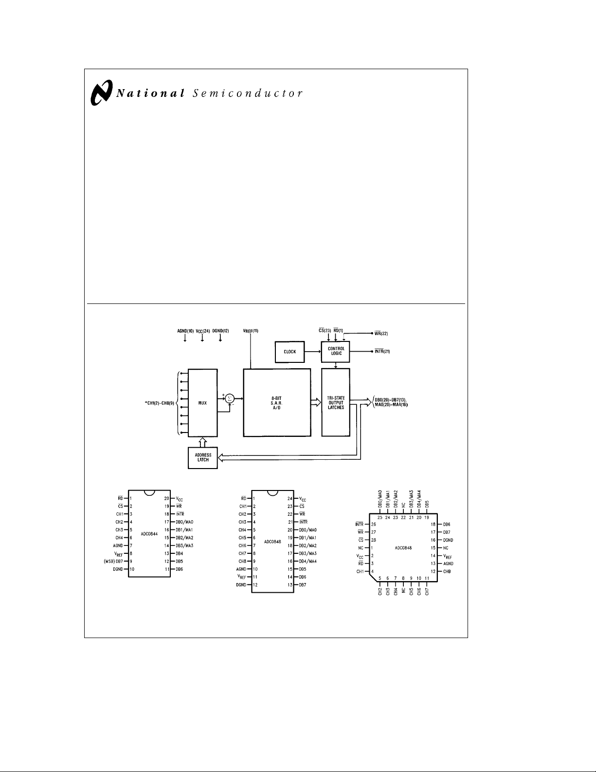
Block and Connection Diagrams
Features
Y
Easy interface to all microprocessors
Y
Operates ratiometrically or with 5 V
voltage reference
Y
No zero or full-scale adjust required
Y
4-channel or 8-channel multiplexer with address logic
Y
Internal clock
Y
0V to 5V input range with single 5V power supply
Y
0.3×standard width 20-pin or 24-pin DIP
Y
28 Pin Molded Chip Carrier Package
DC
Key Specifications
Y
Resolution 8 Bits
Y
Total Unadjusted Error
Y
Single Supply 5 V
Y
Low Power 15 mW
Y
Conversion Time 40 ms
g
(/2 LSB andg1 LSB
ADC0844/ADC0848 8-Bit mP Compatible A/D Converters with Multiplexer Options
DC
*ADC0848 shown in
DIP Package
CH5-CH8 not included
on the ADC0844
Dual-In-Line Package
TL/H/5016– 2
Top View
Dual-In-Line Package
TL/H/5016– 30
Top View
TRI-STATEÉis a registered trademark of National Semiconductor Corp.
C
1995 National Semiconductor Corporation RRD-B30M115/Printed in U. S. A.
TL/H/5016
Molded Chip Carrier Package
Top View
See Ordering Information
TL/H/5016– 1
TL/H/5016– 29
Page 2
Absolute Maximum Ratings (Notes1&2)
If Military/Aerospace specified devices are required,
please contact the National Semiconductor Sales
Office/Distributors for availability and specifications.
Supply Voltage (V
Voltage
Logic Control Inputs
At Other Inputs and Outputs
Input Current at Any Pin (Note 3) 5 mA
Package Input Current (Note 3) 20 mA
Storage Temperature
Package Dissipation at T
ESD Susceptibility (Note 4) 800V
) 6.5V
CC
b
0.3V toa15V
b
0.3V to V
CC
b
e
25§C 875 mW
A
65§Ctoa150§C
a
0.3V
Lead Temperature (Soldering, 10 seconds)
Dual-In-Line Package (Plastic) 260
Dual-In-Line Package (Ceramic) 300
Molded Chip Carrier Package
Vapor Phase (60 seconds) 215
Infrared (15 seconds) 220
Operating Conditions (Notes1&2)
Supply Voltage (VCC) 4.5 VDCto 6.0 V
Temperature Range T
ADC0844BCN, ADC0844CCN, 0§CsT
ADC0848BCN, ADC0848CCN
ADC0844BCJ, ADC0844CCJ,
ADC0848BCJ, ADC0848CCJ
ADC0848BCV, ADC0848CCV
MIN
b
40§CsT
s
s
T
T
A
s
A
s
A
DC
MAX
70§C
85§C
C
§
C
§
C
§
C
§
Electrical Characteristics The following specifications apply for V
Boldface limits apply from T
MIN
to T
MAX
; all other limits T
e
e
T
A
25§C.
j
ADC0844BCJ
ADC0844CCJ
ADC0848BCJ
Typ
(Note 5)
ADC0848CCJ
Tested Design
Limit Limit
(Note 6) (Note 7) (Note 6) (Note 7)
Parameter Conditions
e
5VDCunless otherwise specified.
CC
ADC0844BCN, ADC0844CCN
ADC0848BCN, ADC0848CCN
ADC0848BCV, ADC0848CCV
Tested Design
Typ
(Note 5)
Limit Limit
Limit
Units
CONVERTER AND MULTIPLEXER CHARACTERISTICS
Maximum Total V
Unadjusted Error (Note 8)
ADC0844BCN, ADC0848BCN, BCV
ADC0844BCJ, ADC0848BCJ
ADC0844CCN, ADC0848CCN, CCV
ADC0844CCJ, ADC0848CCJ
REF
e
5.00 V
DC
g
g
(/2 LSB
g
1 LSB
(/2
g
1
g
(/2 LSB
g
1 LSB
Minimum Reference 2.4 1.1 2.4 1.2 1.1 kX
Input Resistance
Maximum Reference 2.4 5.9 2.4 5.4 5.9 kX
Input Resistance
Maximum Common-Mode (Note 9) V
Input Voltage
a
0.05 V
CC
CC
a
0.05 V
CC
a
0.05 V
Minimum Common-Mode (Note 9) GNDb0.05 GNDb0.05 GNDb0.05 V
Input Voltage
DC Common-Mode Error Differential Modeg(/16
Power Supply Sensitivity V
CC
e
5Vg5%
g
(/16
g
(/4
g
(/8
g
g
(/16
(/16
g
(/4
g
(/8
g
(/4 LSB
g
(/8 LSB
Off Channel Leakage (Note 10)
Current On Channel
Off Channel
e
5V,
e
0V
b
1
b
0.1
b
1 mA
On Channele0V, 1 0.1 1 mA
Off Channele5V
DIGITAL AND DC CHARACTERISTICS
V
, Logical ‘‘1’’ Input V
IN(1)
Voltage (Min)
V
, Logical ‘‘0’’ Input V
IN(0)
Voltage (Max)
I
, Logical ‘‘1’’ Input V
IN(1)
Current (Max)
e
5.25V 2.0 2.0 2.0 V
CC
e
4.75V 0.8 0.8 0.8 V
CC
e
5.0V 0.005 1 0.005 1 mA
IN
2
Page 3
Electrical Characteristics The following specifications apply for V
Boldface limits apply from T
MIN
to T
MAX
; all other limits T
e
e
T
A
25§C. (Continued)
j
ADC0844BCJ
ADC0844CCJ
ADC0848BCJ
Typ
(Note 5)
ADC0848CCJ
Tested Design
Limit Limit
(Note 6) (Note 7) (Note 6) (Note 7)
Parameter Conditions
DIGITAL AND DC CHARACTERISTICS (Continued)
I
, Logical ‘‘0’’ Input V
IN(0)
Current (Max)
V
, Logical ‘‘1’’ V
OUT(1)
Output Voltage (Min) I
V
, Logical ‘‘0’’ V
OUT(0)
Output Voltage (Max) I
I
, TRI-STATE Output V
OUT
Current (Max) V
I
, Output Source V
SOURCE
Current (Min)
I
, Output Sink V
SINK
Current (Min)
e
0V
IN
e
4.75V
CC
eb
OUT
eb
I
OUT
e
4.75V 0.4 0.34 0.4 V
CC
e
OUT
e
OUT
e
OUT
e
OUT
e
OUT
ICC, Supply Current (Max) CSe1, V
360 mA 2.4 2.8 2.4 V
10 mA 4.5 4.6 4.5 V
1.6 mA
0V
5V 0.01 3 0..01 0.3 3 mA
0V
V
CC
Open 1 2.5 1 2.3 2.5 mA
REF
b
b
0.005
0.01
b
14
b
1
b
3
b
6.5
16 8.0 16 9.0 8.0 mA
e
5VDCunless otherwise specified.
CC
ADC0844BCN, ADC0844CCN
ADC0848BCN, ADC0848CCN
ADC0848BCV, ADC0848CCV
0.01
14
Tested Design
Limit Limit
b
0.3
b
7.5
Typ
(Note 5)
b
0.005
b
b
b
1 mA
b
3 mA
b
6.5 mA
Limit
Units
AC Electrical Characteristics The following specifications apply for V
otherwise specified. Boldface limits apply from T
MIN
to T
MAX
; all other limits T
e
T
A
Parameter Conditions
e
CC
e
25§C.
j
Typ
(Note 5)
e
r
e
t
f
10 ns unless
5VDC,t
Tested Design
Limit Limit Units
(Note 6) (Note 7)
tC, Maximum Conversion Time (See Graph) 30 40 60 ms
t
, Minimum WR Pulse Width (Note 11) 50 150 ns
W(WR)
t
, Maximum Access Time (Delay from Falling Edge of C
ACC
RD to Output Data Valid) (Note 11)
t1H,t0H, TRI-STATE Control (Maximum Delay from Rising C
Edge of RD
to Hi-Z State) (Note 11)
e
100 pF 145 225 ns
L
L
e
10 pF, R
e
10k 125 200 ns
L
tWI,tRI, Maximum Delay from Falling Edge of WR or RD to (Note 11) 200 400 ns
Reset of INTR
tDS, Minimum Data Set-Up Time (Note 11) 50 100 ns
tDH, Minimum Data Hold Time (Note 11) 0 50 ns
CIN, Capacitance of Logic Inputs 5 pF
C
, Capacitance of Logic Outputs 5 pF
OUT
Note 1: Absolute Maximum Ratings indicate limits beyond which damage to the device may occur. DC and AC electrical specifications do not apply when operating
the device beyond its specified operating conditions.
Note 2: All voltages are measured with respect to the ground pins.
Note 3: When the input voltage (V
limited to 5 mA or less. The 20 mA package input current limits the number of pins that can exceed the power supply boundaries witha5mAcurrent limit to four.
Note 4: Human body model, 100 pF discharged through a 1.5 kX resistor.
Note 5: Typicals are at 25
Note 6: Tested limits are guaranteed to National’s AOQL (Average Outgoing Quality Level).
Note 7: Design limits are guaranteed by not 100% tested. These limits are not used to calculate outgoing quality levels.
Note 8: Total unadjusted error includes offset, full-scale, linearity, and multiplexer error.
) at any pin exceeds the power supply rails (V
IN
C and represent most likely parametric norm.
§
k
IN
Vbor V
l
Va) the absolute value of the current at that pin should be
IN
3
Page 4
Note 9: For VIN(b)tVIN(a) the digital output code will be 0000 0000. Two on-chip diodes are tied to each analog input, which will forward-conduct for analog
input voltages one diode drop below ground or one diode drop greater than V
inputs (5V) can cause this input diode to conduct, especially at elevated temperatures, and cause errors for analog inputs near full-scale. The spec allows 50 mV
forward bias of either diode. This means that as long as the analog V
achieve an absolute 0 V
and loading.
Note 10: Off channel leakage current is measured after the channel selection.
Note 11: The temperature coefficient is 0.3%/
to5VDCinput voltage range will therefore require a minimum supply voltage of 4.950 VDCover temperature variations, initial tolerance
DC
C.
§
IN
supply. Be careful during testing at low VCClevels (4.5V), as high level analog
CC
does not exceed the supply voltage by more than 50 mV, the output code will be correct. To
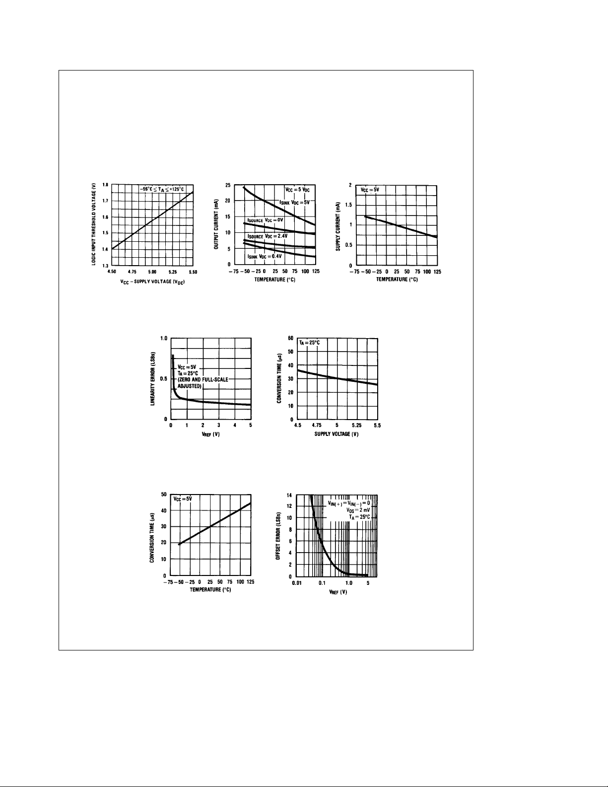
Typical Performance Characteristics
Logic Input Threshold
Voltage vs Supply Voltage
Linearity Error vs V
Output Current vs
Temperature
REF
Power Supply Current vs
Temperature
Conversion Time vs V
SUPPLY
Conversion Time vs
Temperature
Unadjusted Offset Error vs
V
Voltage
REF
TL/H/5016– 3
4
Page 5
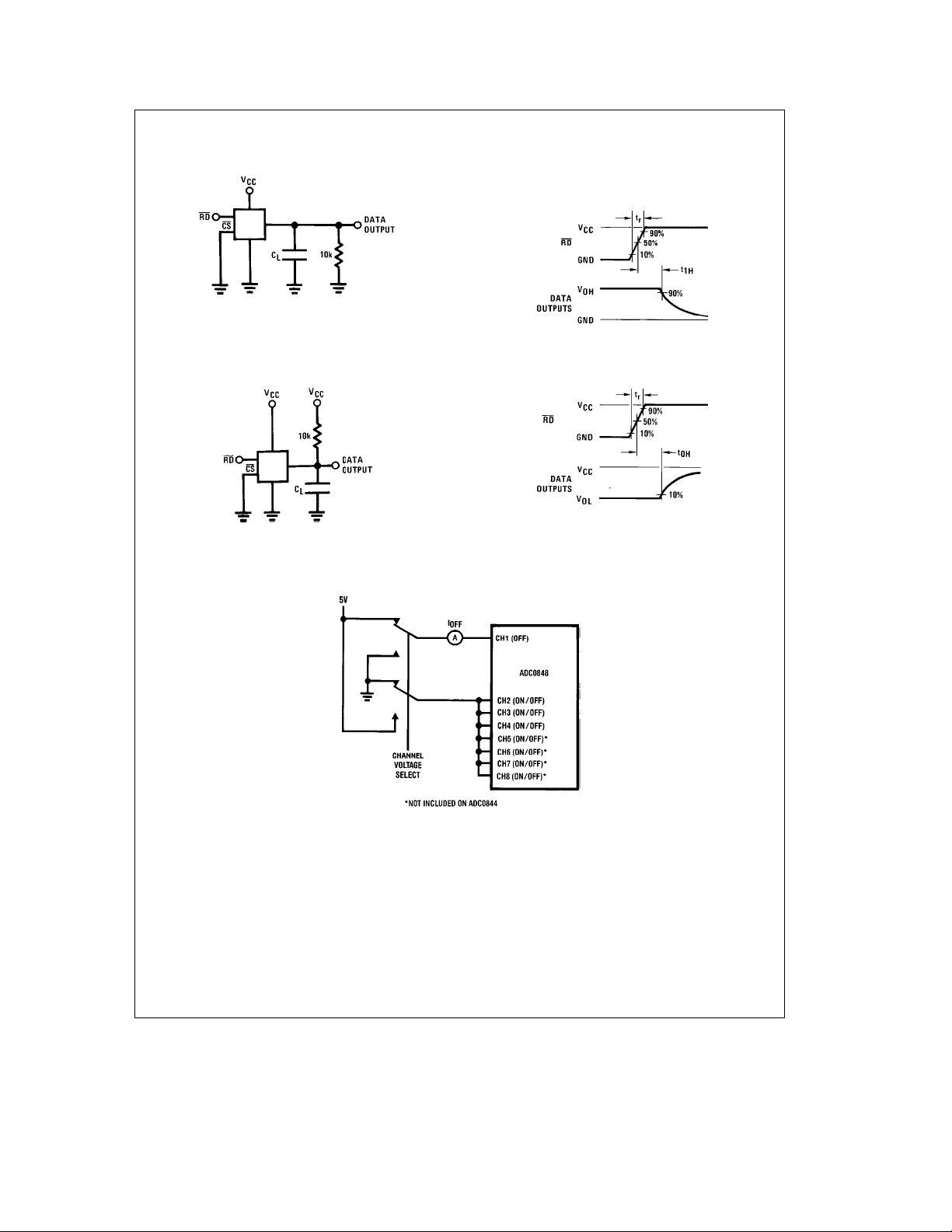
TRI-STATE Test Circuits and Waveforms
t
1H
TL/H/5016– 4
t1H,C
e
10 pF
L
t
0H
Leakage Current Test Circuit
TL/H/5016– 6
t0H,C
e
t
20 ns
r
e
10 pF
L
e
t
20 ns
r
TL/H/5016– 5
TL/H/5016– 7
TL/H/5016– 8
5
Page 6
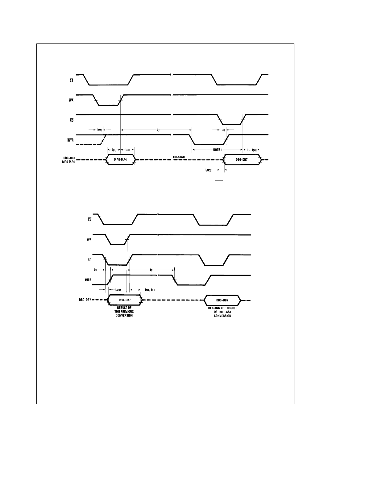
Timing Diagrams
Programming New Channel Configuration and Starting a Conversion
Note 1: Read strobe must occur at least 600 ns after the assertion of interrupt to guarantee reset of INTR.
Note 2: MA stands for MUX address.
Using the Previously Selected Channel Configuration and Starting a Conversion
TL/H/5016– 9
TL/H/5016– 10
6
Page 7

ADC0848 Functional Block Diagram
TL/H/5016– 11
7
Page 8

Functional Description
The ADC0844 and ADC0848 contain a 4-channel and 8channel analog input multiplexer (MUX) respectively. Each
MUX can be configured into one of three modes of operation differential, pseudo-differential, and single ended.
These modes are discussed in the Applications Information
Section. The specific mode is selected by loading the MUX
address latch with the proper address (see Table I and Table II). Inputs to the MUX address latch (MA0-MA4) are
common with data bus lines (DB0-DB4) and are enabled
when the RD
line is high. A conversion is initiated via the CS
and WR lines. If the data from a previous conversion is not
read, the INTR
reset the INTR
cycle. The rising edge of WR
line will be low. The falling edge of WR will
line high and ready the A/D for a conversion
, with RD high, strobes the data
on the MA0/DB0-MA4/DB4 inputs into the MUX address
latch to select a new input configuration and start a conversion. If the RD
WR
the previous MUX configuration is retained, and the
data of the previous conversion is the output on lines DB0DB7. After the conversion cycle (t
by the internal clock frequency, the digital data is trans-
line is held low during the entire low period of
s
40 ms), which is set
C
TABLE I. ADC0844 MUX ADDRESSING
MUX Address
CS
WR RD
MA3 MA2 MA1 MA0 CH1 CH2 CH3 CH4 AGND Mode
XLLLL H
XLLHL
XLHLL H
£
H
XLHHL H
LHLLL H
LHLHL
LHHLL H
£
H
LHHHL H
HHL LL H
HHL HL£H
HHHLL H
XXXXL£L Previous Channel Configuration
Xedon’t care
4 Single-Ended
ferred to the output latch and the INTR
Taking CS
and RD low resets INTR output high and outputs
is asserted low.
the conversion result on the data lines (DB0-DB7).
Applications Information
1.0 MULTIPLEXER CONFIGURATION
The design of these converters utilizes a sampled-data
comparator structure which allows a differential analog input
to be converted by a successive approximation routine.
The actual voltage converted is always the difference between an assigned ‘‘
minal. The polarity of each input terminal of the pair being
converted indicates which line the converter expects to be
the most positive. If the assigned ‘‘
b
‘‘
’’ input the converter responds with an all zeros output
code.
A unique input multiplexing scheme has been utilized to provide multiple analog channels. The input channels can be
software configured into three modes: differential, single-
ab
ba
ab
ab
ab
ab
a
’’ input terminal and a ‘‘b’’ input ter-
a
’’ input is less than the
Ý
Channel
ab
ba
ab
ab
Differential
Single-Ended
Pseudo-
ab
Differential
2 Differential
MUX
3 Pseudo-Differential
FIGURE 1. Analog Input Multiplexer Options
TL/H/5016– 12
TL/H/5016– 14
Combined
TL/H/5016– 13
TL/H/5016– 15
8
Page 9

Applications Information (Continued)
ended, or pseudo-differential.
Figure 1
shows the three
modes using the 4-channel MUX ADC0844. The eight inputs
of the ADC0848 can also be configured in any of the three
modes. In the differential mode, the ADC0844 channel inputs are grouped in pairs, CH1 with CH2 and CH3 with CH4.
The polarity assignment of each channel in the pair is interchangeable. The single-ended mode has CH1 – CH4 assigned as the positive input with the negative input being the
analog ground (AGND) of the device. Finally, in the pseudodifferential mode CH1– CH3 are positive inputs referenced
to CH4 which is now a pseudo-ground. This pseudo-ground
input can be set to any potential within the input commonmode range of the converter. The analog signal conditioning
required in transducer-based data acquisition systems is
significantly simplified with this type of input flexibility. One
converter package can now handle ground referenced inputs and true differential inputs as well as signals with some
arbitrary reference voltage.
The analog input voltages for each channel can range from
50 mV below ground to 50 mV above V
without degrading conversion accuracy.
(typically 5V)
CC
2.0 REFERENCE CONSIDERATIONS
The voltage applied to the reference input of these converters defines the voltage span of the analog input (the difference between V
possible output codes apply. The devices can be used in
IN(MAX)
and V
) over which the 256
IN(MIN)
either ratiometric applications or in systems requiring absolute accuracy. The reference pin must be connected to a
voltage source capable of driving the minimum reference
input resistance of 1.1 kX. This pin is the top of a resistor
TABLE II. ADC0848 MUX Addressing
MUX Address
MA4 MA3 MA2 MA1 MA0 CH1 CH2 CH3 CH4 CH5 CH6 CH7 CH8 AGND Mode
XLLLLL H
XLLLHL H
CS
WR RD
ab
ba
XLLHLL H
XLLHHL
XLHLLL H
£
H
XLHLHL H
XLHHLL H
XLHHHL H
LHLLLL H
ab
LHLLHL H
LHLHLL H
LHLHHL
LHHLLL H
£
H
LHHLHL H
LHHH LL H
LHHHHL H
HHLLLL H
ab
HHL LHL H
HHLHLL H
HHLHHL£H
HHHL LL H
HHHLHL H
HHHHLL H
XXXXXL£L Previous Channel Configuration
divider string used for the successive approximation conversion.
In a ratiometric system (
Figure 2a
), the analog input voltage
is proportional to the voltage used for the A/D reference.
This voltage is typically the system power supply, so the
V
pin can be tied to VCC. This technique relaxes the
REF
stability requirements of the system reference as the analog
input and A/D reference move together maintaining the
same output code for a given input condition.
For absolute accuracy (
Figure 2b
), where the analog input
varies between very specific voltage limits, the reference pin
can be biased with a time and temperature stable voltage
source. The LM385 and LM336 reference diodes are good
low current devices to use with these converters.
The maximum value of the reference is limited to the V
supply voltage. The minimum value, however, can be quite
small (see Typical Performance Characteristics) to allow direct conversions of transducer outputs providing less than a
5V output span. Particular care must be taken with regard to
noise pickup, circuit layout and system error voltage sources when operating with a reduced span due to the increased sensitivity of the converter (1 LSB equals
V
/256).
REF
3.0 THE ANALOG INPUTS
3.1 Analog Differential Voltage Inputs and CommonMode Rejection
The differential input of these converters actually reduces
the effects of common-mode input noise, a signal common
to both selected ‘‘
a
’’ and ‘‘b’’ inputs for a conversion (60
Hz is most typical). The time interval between sampling the
Channel
ab
ba
ab
ba
ab
ba
ab
ab
ab
ab
ab
ab
ab
ab
ab
ab
ab
ab
ab
MUX
Differential
Single-Ended
PseudoDifferential
CC
9
Page 10

Applications Information (Continued)
a
’’ input and then the ‘‘b’’ inputs is (/2 of a clock period.
‘‘
The change in the common-mode voltage during this short
time interval can cause conversion errors. For a sinusoidal
common-mode signal this error is:
t
V
ERROR(MAX)
e
V
(2q fCM)c0.5
peak
where fCMis the frequency of the common-mode signal,
V
is its peak voltage value and tCis the conversion time.
peak
For a 60 Hz common-mode signal to generate a (/4 LSB
error (&5 mV) with the converter running at 40 mS, its peak
value would have to be 5.43V. This large a common-mode
signal is much greater than that generally found in a well
designed data acquisition system.
3.2 Input Current
Due to the sampling nature of the analog inputs, short duration spikes of current enter the ‘‘
a
’’ input and exit the ‘‘b’’
input at the clock edges during the actual conversion. These
currents decay rapidly and do not cause errors as the internal comparator is strobed at the end of a clock period. Bypass capacitors at the inputs will average these currents
and cause an effective DC current to flow through the output resistance of the analog signal source. Bypass capacitors should not be used if the source resistance is greater
than 1 kX.
3.3 Input Source Resistance
The limitation of the input source resistance due to the DC
leakage currents of the input multiplexer is important. A
worst-case leakage current of
g
1 mA over temperature will
createa1mVinput error witha1kXsource resistance. An
op amp RC active low pass filter can provide both impedance buffering and noise filtering should a high impedance
signal source be required.
C
c
8
#
J
4.0 OPTIONAL ADJUSTMENTS
4.1 Zero Error
The zero of the A/D does not require adjustment. If the
minimum analog input voltage value, V
a zero offset can be done. The converter can be made to
IN(MIN)
, is not ground,
output 0000 0000 digital code for this minimum input voltage
by biasing any V
useful for either differential or pseudo-differential modes of
(b) input at this V
IN
IN(MIN)
value. This is
input channel configuration.
The zero error of the A/D converter relates to the location
of the first riser of the transfer function and can be measured by grounding the V
nitude positive voltage to the V
b
input and applying a small mag-
a
input. Zero error is the
difference between actual DC input voltage which is necessary to just cause an output digital code transition from 0000
0000 to 0000 0001 and the ideal (/2 LSB value ((/2 LSB
mV for V
REF
e
5.000 VDC).
e
9.8
4.2 Full-Scale
The full-scale adjustment can be made by applying a differential input voltage which is 1 (/2 LSB down from the desired
analog full-scale voltage range and then adjusting the magnitude of the V
from 1111 1110 to 1111 1111.
input for a digital output code changing
REF
4.3 Adjusting for an Arbitrary Analog Input Voltage
Range
If the analog zero voltage of the A/D is shifted away from
ground (for example, to accommodate an analog input signal which does not go to ground), this new zero reference
should be properly adjusted first. A V
equals this desired zero reference plus (/2 LSB (where the
(a) voltage which
IN
LSB is calculated for the desired analog span, 1 LSB
analog span/256) is applied to selected ‘‘a’’ input and the
zero reference voltage at the corresponding ‘‘
should then be adjusted to just obtain the 00
code transition.
HEX
b
’’ input
to 01
HEX
e
a) Ratiometric
TL/H/5016– 16
FIGURE 2. Referencing Examples
10
TL/H/5016– 17
b) Absolute with a Reduced Span
Page 11

Applications Information (Continued)
The full-scale adjustment should be made[with the proper
V
(b) voltage applied]by forcing a voltage to the VIN(a)
IN
input which is given by:
(a)fsadjeV
V
IN
where V
e
the high end of the analog input range and
MAX
MAX
b
1.5
b
(V
V
MAX
Ð
)
MIN
256
(
Zero-Shift and Span Adjust (2V
e
the low end (the offset zero) of the analog range.
V
MIN
(Both are ground referenced.)
The V
code change from FE
justment procedure.
For an example see the Zero-Shift and Span Adjust circuit
below.
(or VCC) voltage is then adjusted to provide a
REF
s
s
V
5V)
IN
HEX
to FF
. This completes the ad-
HEX
TL/H/5016– 18
11
Page 12

Applications Information (Continued)
Differential Voltage Input 9-Bit A/D
TL/H/5016– 19
Span Adjust 0VsV
Protecting the Input
s
3V
IN
TL/H/5016– 20
Diodes are 1N914
TL/H/5016– 21
12
Page 13

Applications Information (Continued)
High Accuracy Comparators
DOeall 1s if VIN(a)lVIN(b)
e
DO
all 0s if VIN(a)kVIN(b)
*VIN(b)e0.15 V
15% of V
TL/H/5016– 22
Operating with Automotive Ratiometric Transducers
CC
s
s
V
XDR
85% of V
CC
CC
TL/H/5016– 23
13
Page 14

Applications Information (Continued)
A Stand Alone Circuit
Note: DUT pin numbers in parentheses are for ADC0844, others are for ADC0848.
Start a Conversion without Updating the Channel Configuration
CS#WR will update the channel configuration and start a conversion.
CS
RD will read the conversion data and start a new conversion without updat-
#
ing the channel configuration.
Waiting for the end of this conversion is not necessary. A CS
ately follow the CS
RD.
#
WR can immedi-
#
14
TL/H/5016– 25
TL/H/5016– 26
Page 15

Applications Information (Continued)
ADC0844ÐINS8039 Interface
SAMPLE PROGRAM FOR ADC0844ÐINS8039 INTERFACE
CONVERTING TWO RATIOMETRIC, DIFFERENTIAL SIGNALS
0000 04 10 JMP BEGIN ;START PROGRAM AT ADDR 10
0010 B9 FF BEGIN: MOV R1,
0012 B8 20 MOV R0,
0014 89 FF ORL P1,
0016 23 00 MOV A,00H ;LOAD THE ACC WITH A/D MUX DATA
0018 14 50 CALL CONV ;CALL THE CONVERSION SUBROUTINE
001A 23 02 MOV A,
001C 18 INC R0 ;INCREMENT THE A/D DATA ADDRESS
001D 14 50 CALL CONV ;CALL THE CONVERSION SUBROUTINE
ORG 0H
ORG 10H ;MAIN PROGRAM
Ý
0FFH ;LOAD R1 WITH A UNUSED ADDR
;LOCATION
Ý
20H ;A/D DATA ADDRESS
Ý
0FFH ;SET PORT 1 OUTPUTS HIGH
;CH1 AND CH2 DIFFERENTIAL
Ý
02H ;LOAD THE ACC WITH A/D MUX DATA
;CH3 AND CH4 DIFFERENTIAL
TL/H/5016– 27
;CONTINUE MAIN PROGRAM
;CONVERSION SUBROUTINE
;ENTRY:ACCÐA/D MUX DATA
;EXIT: ACCÐCONVERTED DATA
ORG 50H
0050 99 FE CONV: ANL P1,
0052 91 MOVX
0053 09 LOOP: IN A,P1 ;INPUT INTR
0054 32 53 JB1 LOOP ;IF INTR
0056 81 MOVX A,
Ý
0FEH ;CHIP SELECT THE A/D
@
R1,A ;LOAD A/D MUX & START CONVERSION
STATE
e
@
R1 ;IF INTRe0 INPUT A/D DATA
1 GOTO LOOP
0057 89 01 ORL P1,&01H ;CLEAR THE A/D CHIP SELECT
0059 A0 MOV
@
R0,A ;STORE THE A/D DATA
005A 83 RET ;RETURN TO MAIN PROGRAM
15
Page 16

Applications Information (Continued)
I/O Interface to NSC800
TL/H/5016– 28
SAMPLE PROGRAM FOR ADC0848ÐNSC800 INTERFACE
0008 NCONV EQU 16
000F DEL EQU 15 ;DELAY 50 msec CONVERSION
001F CS EQU 1FH ;THE BOARD ADDRESS
3C00 ADDTA EQU 003CH ;START OF RAM FOR A/D
0000
0004
0008
000A
000C
000F
0012
0014
0015
0017
0018
001B
001D
001E
08 09 0A 0B MUXDTA: DB 08H,09H,0AH,0BH ;MUX DATA
Ê
0C 0D 0E 0F DB 0CH,0DH,0EH,0FH
Ê
0E 1F START: LD C,CS
Ê
06 16 LD B,NCONV
Ê
21 0000
Ê
Ê
Ê
Ê
Ê
Ê
Ê
Ê
Ê
Ê
Ê
11 003C LD DE,ADDTA
ED A3 STCONV: OUTI ;LOAD A/D’S MUX DATA
EB EX DE,HL ;HLeRAM ADDRESS FOR THE
3E 0F LD A,DEL
3D WAIT: DEC A ;WAIT 50 msec FOR THE
C2 0013
Ê
ED A2 INI ;STORE THE A/D’S DATA
EB EX DE,HL
C2 000E
Ê
LD HL,MUXDTA
JP NZ,WAIT ;CONVERSION TO FINISH
JP NZ,STCONV ;IF NOT GOTO STCONV
;DATA
;AND START A CONVERSION
;A/D DATA
;CONVERTED ALL INPUTS?
Note: This routine sequentially programs the MUX data latch in the signal-ended mode. For CH1-CH8 a conversion is started, then a 50 ms wait for the A/D to
complete a conversion and the data is stored at address ADDTA for CH1, ADDTA
END
16
a
1 for CH2, etc.
Page 17

Ordering Information
Temperature Total Unadjusted Error MUX Package
Range
Ctoa70§C
0
§
b
40§Ctoa85§C
g
(/2 LSB
ADC0844BCN
ADC0848BCN
ADC0844BCJ
ADC0848BCJ
ADC0848BCV
g
1 LSB
ADC0844CCN Molded Dip
ADC0848CCN Molded Dip
ADC0844CCJ Cerdip
ADC0848CCJ Cerdip
ADC0848CCV Molded Chip Carrier
Channels Outline
4
8
4
8
8
N20A
N24C
J20A
J24F
V28A
17
Page 18

Physical Dimensions inches (millimeters)
Ceramic Dual-In-Line Package (J)
NS Package Number J20A
Cavity Dual-In-Line Package (J)
NS Package Number J24F
18
Page 19

Physical Dimensions inches (millimeters) (Continued)
Molded Dual-In-Line Package (N)
NS Package Number N20A
Molded Dual-In-Line Package (N)
NS Package Number N24C
19
Page 20

Physical Dimensions inches (millimeters) (Continued)
Molded Chip Carrier Package (V)
NS Package Number V28A
LIFE SUPPORT POLICY
NATIONAL’S PRODUCTS ARE NOT AUTHORIZED FOR USE AS CRITICAL COMPONENTS IN LIFE SUPPORT
DEVICES OR SYSTEMS WITHOUT THE EXPRESS WRITTEN APPROVAL OF THE PRESIDENT OF NATIONAL
SEMICONDUCTOR CORPORATION. As used herein:
1. Life support devices or systems are devices or 2. A critical component is any component of a life
systems which, (a) are intended for surgical implant support device or system whose failure to perform can
into the body, or (b) support or sustain life, and whose be reasonably expected to cause the failure of the life
failure to perform, when properly used in accordance support device or system, or to affect its safety or
ADC0844/ADC0848 8-Bit mP Compatible A/D Converters with Multiplexer Options
with instructions for use provided in the labeling, can effectiveness.
be reasonably expected to result in a significant injury
to the user.
National Semiconductor National Semiconductor National Semiconductor National Semiconductor
Corporation Europe Hong Kong Ltd. Japan Ltd.
1111 West Bardin Road Fax: (
Arlington, TX 76017 Email: cnjwge@tevm2.nsc.com Ocean Centre, 5 Canton Rd. Fax: 81-043-299-2408
Tel: 1(800) 272-9959 Deutsch Tel: (
Fax: 1(800) 737-7018 English Tel: (
National does not assume any responsibility for use of any circuitry described, no circuit patent licenses are implied and National reserves the right at any time without notice to change said circuitry and specifications.
Fran3ais Tel: (
Italiano Tel: (
a
49) 0-180-530 85 86 13th Floor, Straight Block, Tel: 81-043-299-2309
a
49) 0-180-530 85 85 Tsimshatsui, Kowloon
a
49) 0-180-532 78 32 Hong Kong
a
49) 0-180-532 93 58 Tel: (852) 2737-1600
a
49) 0-180-534 16 80 Fax: (852) 2736-9960
 Loading...