Page 1
ADC0820 8-Bit High Speed mP Compatible
A/D Converter with Track/Hold Function
ADC0820 8-Bit High Speed mP Compatible A/D Converter with Track/Hold Function
February 1995
General Description
By using a half-flash conversion technique, the 8-bit
ADC0820 CMOS A/D offers a 1.5 ms conversion time and
dissipates only 75 mW of power. The half-flash technique
consists of 32 comparators, a most significant 4-bit ADC
and a least significant 4-bit ADC.
The input to the ADC0820 is tracked and held by the input
sampling circuitry eliminating the need for an external sample-and-hold for signals moving at less than 100 mV/ms.
For ease of interface to microprocessors, the ADC0820 has
been designed to appear as a memory location or I/O port
without the need for external interfacing logic.
Key Specifications
Y
Resolution 8 Bits
Y
Conversion Time 2.5 ms Max (RD Mode)
1.5 ms Max (WR-RD Mode)
Y
Input signals with slew rate of 100 mV/ms converted
without external sample-and-hold to 8 bits
Y
Low Power 75 mW Max
Y
Total Unadjusted Error
g
(/2 LSB andg1 LSB
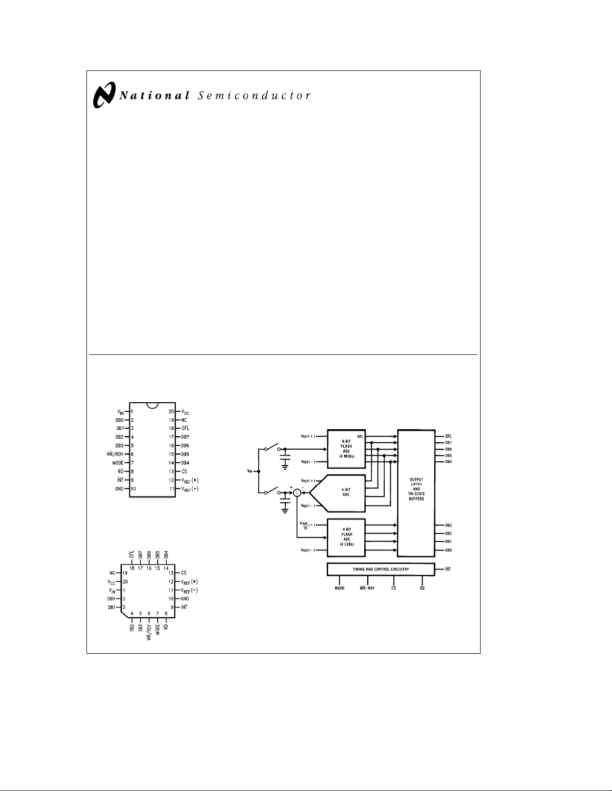
Connection and Functional Diagrams
Dual-In-Line, Small Outline and
SSOP Packages
Features
Y
Built-in track-and-hold function
Y
No missing codes
Y
No external clocking
Y
Single supplyÐ5 V
Y
Easy interface to all microprocessors, or operates
stand-alone
Y
Latched TRI-STATEÉoutput
Y
Logic inputs and outputs meet both MOS and T2L voltage level specifications
Y
Operates ratiometrically or with any reference value
equal to or less than V
Y
0V to 5V analog input voltage range with single 5V
supply
Y
No zero or full-scale adjust required
Y
Overflow output available for cascading
Y
0.3×standard width 20-pin DIP
Y
20-pin molded chip carrier package
Y
20-pin small outline package
Y
20-pin shrink small outline package (SSOP)
DC
CC
Top View
TL/H/5501– 1
Molded Chip Carrier
Package
FIGURE 1
TL/H/5501– 2
TRI-STATEÉis a registered trademark of National Semiconductor Corporation.
C
1995 National Semiconductor Corporation RRD-B30M115/Printed in U. S. A.
TL/H/5501– 33
TL/H/5501
See Ordering Information
Page 2
Absolute Maximum Ratings (Notes1&2)
If Military/Aerospace specified devices are required,
please contact the National Semiconductor Sales
Office/Distributors for availability and specifications.
Supply Voltage (V
Logic Control Inputs
Voltage at Other Inputs and Output
Storage Temperature Range
Package Dissipation at T
) 10V
CC
e
A
b
0.2V to V
b
CC
0.2V to V
CC
b
65§Ctoa150§C
25§C 875 mW
a
0.2V
a
0.2V
Input Current at Any Pin (Note 5) 1 mA
Package Input Current (Note 5) 4 mA
ESD Susceptability (Note 9) 1200V
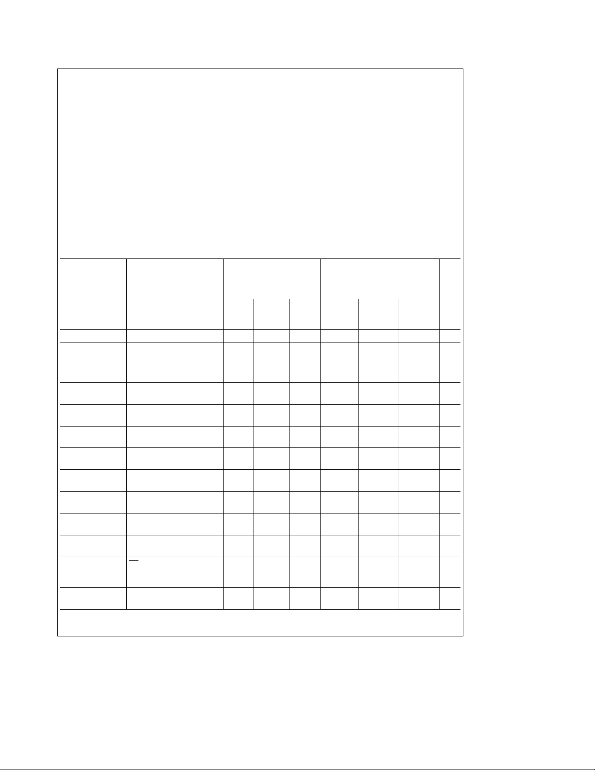
Converter Characteristics The following specifications apply for RD mode (pin 7
and V
Resolution 8 8 8 Bits
Total Unadjusted ADC0820BCN, BCWM
Error ADC0820CCJ
(Note 3) ADC0820CCN, CCWM, CIWM,
Minimum Reference 2.3 1.00 2.3 1.2 kX
Resistance
Maximum Reference 2.3 6 2.3 5.3 6 kX
Resistance
Maximum V
Input Voltage
Minimum V
Input Voltage
Minimum V
Input Voltage
Maximum V
Input Voltage
Maximum VINInput V
Voltage
Minimum VINInput GNDb0.1 GNDb0.1 GNDb0.1 V
Voltage
Maximum Analog CSeV
Input Leakage V
Current V
Power Supply V
Sensitivity
(b)eGND unless otherwise specified. Boldface limits apply from T
REF
Parameter Conditions
Typ
(Note 6)
ADC0820CCMSA
(a) V
REF
(b) GND GND GND V
REF
(a) V
REF
(b) V
REF
CC
e
V
IN
CC
e
GND
IN
CC
e
5Vg5%
g
(/16
Lead Temp. (Soldering, 10 sec.)
Dual-In-Line Package (plastic) 260
Dual-In-Line Package (ceramic) 300
Surface Mount Package
Vapor Phase (60 sec.) 215
Infrared (15 sec.) 220
Operating Ratings (Notes1&2)
Temperature Range T
ADC0820CCJ
ADC0820CIWM
ADC0820BCN, ADC0820CCN 0
ADC0820BCV, ADC0820CCV 0
ADC0820BCWM, ADC0820CCWM 0
ADC0820CCMSA 0
VCCRange 4.5V to 8V
e
MIN
to T
0), V
; all other limits T
MAX
ADC0820BCN, ADC0820CCN
ADC0820CCJ
ADC0820BCV, ADC0820CCV
ADC0820BCWM, ADC0820CCWM
ADC0820CCMSA, ADC0820CIWM
Tested Design
Limit Limit
(Note 7) (Note 8) (Note 7) (Note 8)
g
1 LSB
CC
(b) V
REF
(a) V
REF
a
0.1 V
CC
Typ
(Note 6)
Tested Design
Limit Limit
g
g
g
V
REF
REF
CC
3 0.3 3 mA
b
3
g
(/4
g
(/16
b
g
b
b
e
CC
(/2
1
1
CC
(b) V
(a) V
a
0.1 V
0.3
(/4
MIN
40§CsT
40§CsT
5V, V
s
T
A
s
A
s
A
CsT
§
A
CsT
§
A
CsT
§
A
CsT
§
A
(a)e5V,
REF
e
T
A
j
g
(/2 LSB
g
1 LSB
g
1 LSB
V
CC
(b) V
REF
(a) V
REF
a
0.1 V
CC
b
3 mA
g
(/4 LSB
s
a
a
s
s
s
s
e
T
MAX
85§C
85§C
70§C
70§C
70§C
70§C
25§C.
Limit
Units
C
§
C
§
C
§
C
§
V
2
Page 3
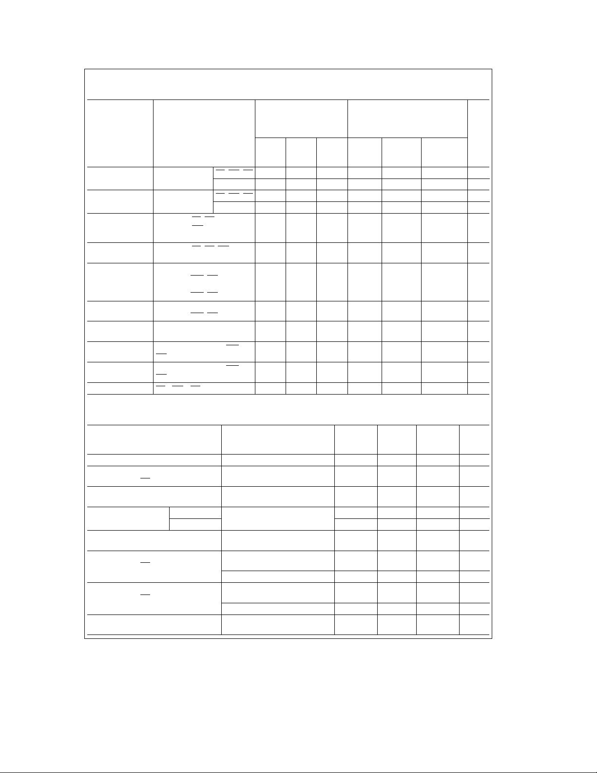
DC Electrical Characteristics The following specifications apply for V
Boldface limits apply from T
MIN
to T
MAX
; all other limits T
e
e
T
25§C.
A
J
ADC0820CCJ
Parameter Conditions
Tested Design
V
, Logical ‘‘1’’ V
IN(1)
Input Voltage
V
, Logical ‘‘0’’ V
IN(0)
Input Voltage
I
, Logical ‘‘1’’ V
IN(1)
Input Current V
I
, Logical ‘‘0’’ V
IN(0)
Input Current Mode
V
, Logical ‘‘1’’ V
OUT(1)
Output Voltage DB0– DB7, OFL, INT
V
, Logical ‘‘0’’ V
OUT(0)
Output Voltage DB0– DB7, OFL
I
, TRI-STATE V
OUT
Output Current V
I
, Output V
SOURCE
Source Current INT
I
, Output Sink V
SINK
Current INT, RDY
ICC, Supply Current CS
e
5.25V CS,WR,RD 2.0 2.0 2.0 V
CC
e
4.75V CS,WR,RD 0.8 0.8 0.8 V
CC
e
5V; CS,RD 0.005 1 0.005 1 mA
IN(1)
e
5V; WR 0.1 3 0.1 0.3 3 mA
IN(1)
e
V
5V; Mode 50 200 50 170 200 mA
IN(1)
e
0V; CS,RD,WR,
IN(0)
e
4.75V, I
CC
e
V
CC
DB0–DB7, OFL
e
CC
OUT
OUT
OUT
OUT
eWReRDe
OUT
4.75V, I
OUT
, INT
4.75V, I
OUT
, INT, RDY
e
5V; DB0–DB7, RDY 0.1 3 0.1 0.3 3 mA
e
0V; DB0–DB7, RDY
e
0V; DB0–DB7, OFL
e
5V; DB0–DB7, OFL,147 14 8.4 7 mA
0 7.5 15 7.5 13 15 mA
Typ
(Note 6)
Mode 3.5 3.5 3.5 V
Mode 1.5 1.5 1.5 V
b
eb
360 mA; 2.4 2.8 2.4 V
eb
10 mA; 4.5 4.6 4.5 V
e
1.6 mA; 0.4 0.34 0.4 V
b
b
Limit Limit
(Note 7) (Note 8) (Note 7) (Note 8)
0.1
12
b
1
b
3
b
6
b
9
4.0
0.005
b
e
5V, unless otherwise specified.
CC
ADC0820BCN, ADC0820CCN
ADC0820BCV, ADC0820CCV
ADC0820BCWM, ADC0820CCWM
ADC0820CCMSA, ADC0820CIWM
Typ
(Note 6)
b
0.005
b
b
b
Tested Design
Limit Limit
0.1
12
b
b
b
9
0.3
7.2
5.3
b
1 mA
b
3 mA
b
6 mA
b
4.0 mA
Limit
Units
AC Electrical Characteristics The following specifications apply for V
V
(b)e0V and T
REF
t
, Conversion Time for RD Mode Pin 7e0,
CRD
t
, Access Time (Delay from Pin 7e0,
ACC0
Falling Edge of RD
t
, Conversion Time for Pin 7eVCC;t
CWR-RD
WR-RD Mode t
tWR, Write Time Min Pin 7eVCC;
e
25§C unless otherwise specified.
A
Parameter Conditions
(Figure 2)
(Figure 2)
to Output Valid)
600 ns;
WR
(Figures 3a
RD
e
e
(Figures 3a
(Note 6)
t
CRD
600 ns, 1.52 ms
and
3b)
and
3b)
Max (Note 4) See Graph 50 ms
tRD, Read Time Min Pin 7eVCC;
(Figures 3a
and
3b)
(Note 4) See Graph
e
1k and C
RD
RD
k
tI;
(Figure 3a)
l
tI;
(Figure 3b)
e
15 pF 30 ns
L
t
, Access Time (Delay from Pin 7eVCC,t
ACC1
Falling Edge of RD to Output Valid) C
C
t
, Access Time (Delay from Pin 7eVCC,t
ACC2
Falling Edge of RD to Output Valid) C
C
t
, Access Time (Delay from Rising R
ACC3
Edge of RDY to Output Valid)
e
15 pF 190 280 ns
L
e
100 pF 210 320 ns
L
e
15 pF 70 120 ns
L
e
100 pF 90 150 ns
L
PULLUP
3
e
e
e
5V, t
t
Typ
CC
20 ns, V
r
f
Tested Design
Limit Limit Units
REF
(a)e5V,
(Note 7) (Note 8)
1.6 2.5 ms
a
20 t
CRD
a
50 ns
600 ns
600 ns
Page 4
e
e
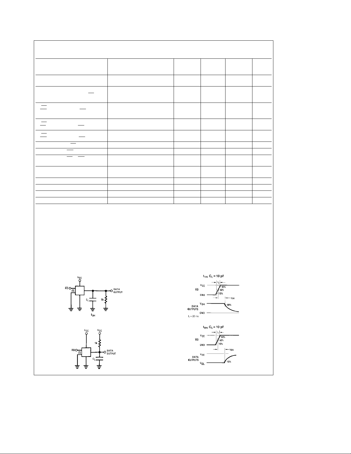
AC Electrical Characteristics (Continued) The following specifications apply for V
V
(a)e5V, V
REF
tI, Internal Comparison Time Pin 7eVCC;
t1H,t0H, TRI-STATE Control R
(Delay from Rising Edge of RD
(b)e0V and T
REF
Parameter Conditions
e
25§C unless otherwise specified.
A
e
C
50 pF
L
e
1k, C
L
to
L
Typ
(Note 6)
(Figures 3b
e
10 pF 100 200 ns
and
4)
800 1300 ns
Tested Design
Limit Limit Units
(Note 7) (Note 8)
CC
5V, t
e
t
20 ns,
r
f
Hi-Z State)
t
, Delay from Rising Edge of Pin 7eVCC,C
INTL
WR
to Falling Edge of INT t
t
, Delay from Rising Edge of
INTH
RD
to Rising Edge of INT C
t
, Delay from Rising Edge of
INTHWR
WR
to Rising Edge of INT
t
, Delay from CS to RDY
RDY
tID, Delay from INT to Output Valid
l
tI;
RD
k
t
tI;
RD
(Figures 2, 3a
e
50 pF
L
(Figure 4)
(Figure 2)
(Figure 4)
tRI, Delay from RD to INT Pin 7eVCC,t
(Figure 3a)
tP, Delay from End of Conversion
(Figures 2, 3a, 3b
e
50 pF
L
(Figure 3b)
(Figure 3a)
and
3b)
e
,C
50 pF 175 270 ns
L
e
,C
50 pF, Pin 7e0 50 100 ns
L
a
t
200 t
RD
125 225 ns
20 50 ns
k
RD
t
I
and
4)
200 290 ns
t
I
a
290 ns
RD
500 ns
ns
to Next Conversion (Note 4) See Graph
Slew Rate, Tracking 0.1 V/ms
C
, Analog Input Capacitance 45 pF
VIN
C
, Logic Output Capacitance 5 pF
OUT
CIN, Logic Input Capacitance 5 pF
Note 1: Absolute Maximum Ratings indicate limits beyond which damage to the device may occur. DC and AC electrical specifications do not apply when operating
the device beyond its specified operating conditions.
Note 2: All voltages are measured with respect to the GND pin, unless otherwise specified.
Note 3: Total unadjusted error includes offset, full-scale, and linearity errors.
Note 4: Accuracy may degrade if t
Note 5: When the input voltage (V
to 1 mA or less. The 4 mA package input current limits the number of pins that can exceed the power supply boundaries witha1mAcurrent limit to four.
Note 6: Typicals are at 25
Note 7: Tested limits are guaranteed to National’s AOQL (Average Outgoing Quality Level).
Note 8: Design limits are guaranteed but not 100% tested. These limits are not used to calculate outgoing quality levels.
Note 9: Human body model, 100 pF discharaged through a 1.5 kX resistor.
§
or tRDis shorter than the minimum value specified. See Accuracy vs tWRand Accuracy vs tRDgraphs.
WR
) at any pin exceeds the power supply rails (V
IN
C and represent most likely parametric norm.
k
IN
Vbor V
l
Va) the absolute value of current at that pin should be limited
IN
TRI-STATE Test Circuits and Waveforms
t
1H
TL/H/5501– 3
t
0H
TL/H/5501– 5
4
TL/H/5501– 4
e
t
20 ns TL/H/5501 – 6
r
Page 5
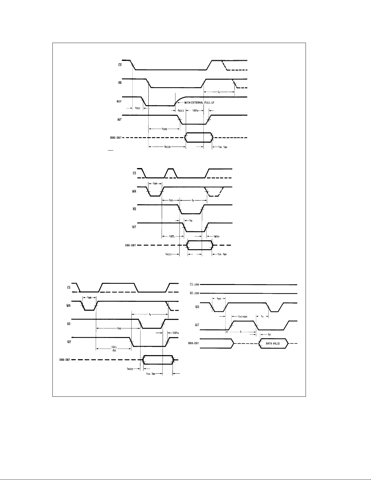
Timing Diagrams
Note: On power-up the state of INT can be high or low.
FIGURE 3a. WR-RD Mode (Pin 7 is High and t
FIGURE 2. RD Mode (Pin 7 is Low)
RD
TL/H/5501– 7
TL/H/5501– 8
k
tI)
FIGURE 3b. WR-RD Mode (Pin 7 is High and t
RD
l
TL/H/5501– 10
FIGURE 4. WR-RD Mode (Pin 7 is High)
Stand-Alone Operation
TL/H/5501– 9
tI)
5
Page 6
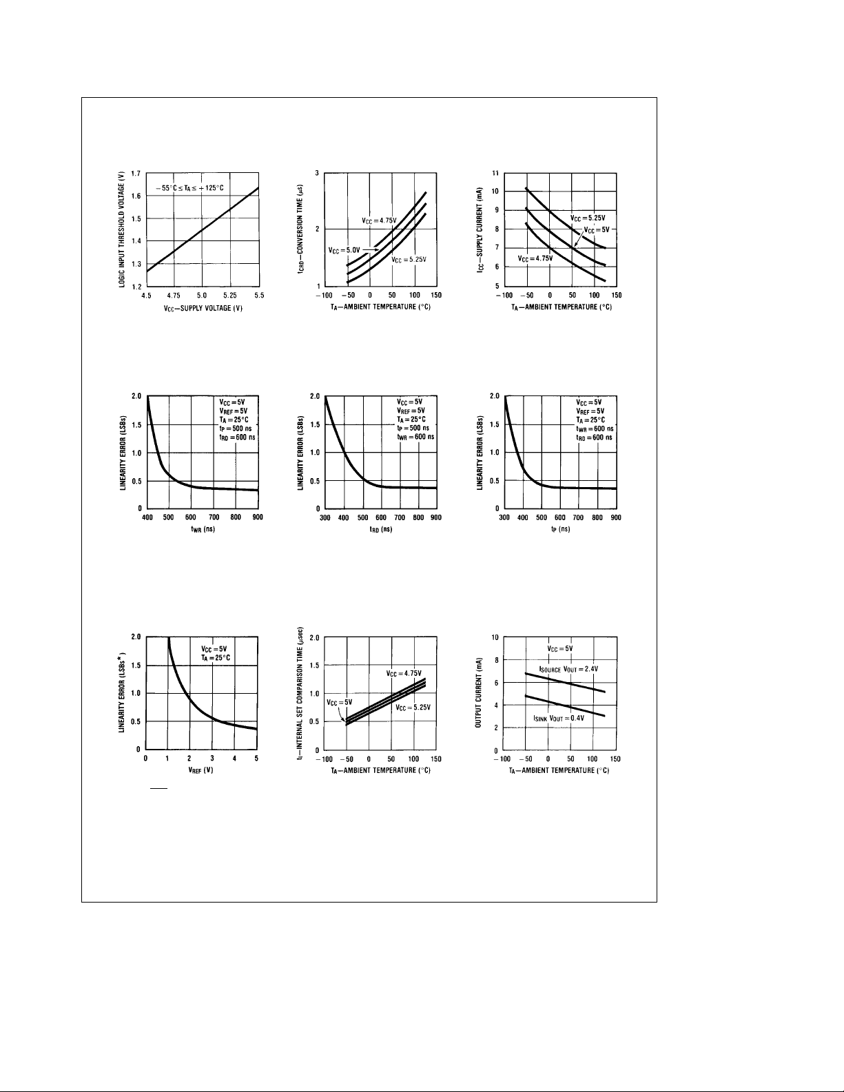
Typical Performance Characteristics
Logic Input Threshold
Voltage vs Supply Voltage
Conversion Time (RD Mode)
vs Temperature
Power Supply Current vs
Temperature (not including
reference ladder)
*1 LSB
e
Accuracy vs t
Accuracy vs V
e
[
V
V
REF
REF
V
REF
256
WR
REF
(a)bV
REF
(b)
Accuracy vs t
RD
tI, Internal Time Delay vs
]
Temperature
Accuracy vs t
p
Output Current vs
Temperature
TL/H/5501– 11
6
Page 7

Description of Pin Functions
Pin Name Function
1VINAnalog input; rangeeGNDsV
2 DB0 TRI-STATE data outputÐbit 0 (LSB)
3 DB1 TRI-STATE data outputÐbit 1
4 DB2 TRI-STATE data outputÐbit 2
5 DB3 TRI-STATE data outputÐbit 3
6WR
/RDY WR-RD Mode
WR
: With CS low, the conversion is start-
ed on the falling edge of WR
mately 800 ns (the preset internal time
out, t
) after the WR rising edge, the result
I
of the conversion will be strobed into the
output latch, provided that RD
occur prior to this time out (see
3a
and3b).
RD Mode
RDY: This is an open drain output (no in-
ternal pull-up device). RDY will go low after the falling edge of CS
TRI-STATE when the result of the conversion is strobed into the output latch. It is
used to simplify the interface to a microprocessor system (see
7 Mode Mode: Mode selection inputÐit is inter-
nally tied to GND through a 50 mA current
source.
RD Mode: When mode is low
WR-RD Mode: When mode is high
8RD
WR-RD Mode
With CS
low, the TRI-STATE data outputs
(DB0-DB7) will be activated when RD
goes low (see
Figure 4
used to increase the speed of the converter by reading data prior to the preset
internal time out (t
done, the data result transferred to output
,E800 ns). If this is
I
latch is latched after the falling edge of
the RD
(see
Figures 3a
RD Mode
With CS
low, the conversion will start with
RD
going low, also RD will enable the
TRI-STATE data outputs at the completion of the conversion. RDY going TRISTATE and INT
going low indicates the
completion of the conversion (see
2
).
s
V
IN
CC
. Approxi-
does not
Figures
; RDY will go
Figure 2
).
). RD can also be
and3b).
Figure
Pin Name Function
9 INT WR-RD Mode
INT
going low indicates that the conversion is completed and the data result is in
the output latch. INT
(the preset internal time out, t
rising edge of WR
will go low,E800 ns
) after the
Figure 3b
I
); or INT
(see
will go low after the falling edge of RD,if
RD
goes low prior to the 800 ns time out
(see
Figure 3a
edge of RD
3b
).
). INT is reset by the rising
or CS (see
Figures 3a
RD Mode
INT
going low indicates that the conversion is completed and the data result is in
the output latch. INT
edge of RD
is reset by the rising
or CS (see
Figure 2
).
10 GND Ground
11 V
12 V
13 CS
(b) The bottom of resistor ladder, voltage
REF
range: GND
5)
(a) The top of resistor ladder, voltage range:
REF
V
REF
CS must be low in order for the RD or WR
(b)sV
s
V
(b)sV
REF
(a)sVCC(Note 5)
REF
(a) (Note
REF
to be recognized by the converter.
14 DB4 TRI-STATE data outputÐbit 4
15 DB5 TRI-STATE data outputÐbit 5
16 DB6 TRI-STATE data outputÐbit 6
17 DB7 TRI-STATE data outputÐbit 7 (MSB)
18 OFL
Overflow outputÐIf the analog input is
higher than the V
at the end of conversion. It can be used to
(a), OFL will be low
REF
cascade 2 or more devices to have more
resolution (9, 10-bit). This output is always
active and does not go into TRI-STATE
as DB0 – DB7 do.
19 NC No connection
20 V
CC
Power supply voltage
and
1.0 Functional Description
1.1 GENERAL OPERATION
The ADC0820 uses two 4-bit flash A/D converters to make
an 8-bit measurement (
up of 15 comparators which compare the unknown input to
a reference ladder to get a 4-bit result. To take a full 8-bit
reading, one flash conversion is done to provide the 4 most
significant data bits (via the MS flash ADC). Driven by the 4
MSBs, an internal DAC recreates an analog approximation
of the input voltage. This analog signal is then subtracted
from the input, and the difference voltage is converted by a
second 4-bit flash ADC (the LS ADC), providing the 4 least
significant bits of the output data word.
Figure 1
). Each flash ADC is made
The internal DAC is actually a subsection of the MS flash
converter. This is accomplished by using the same resistor
ladder for the A/D as well as for generating the DAC signal.
The DAC output is actually the tap on the resistor ladder
which most closely approximates the analog input. In addition, the ‘’sampled-data’’ comparators used in the ADC0820
provide the ability to compare the magnitudes of several
analog signals simultaneously, without using input summing
amplifiers. This is especially useful in the LS flash ADC,
where the signal to be converted is an analog difference.
7
Page 8
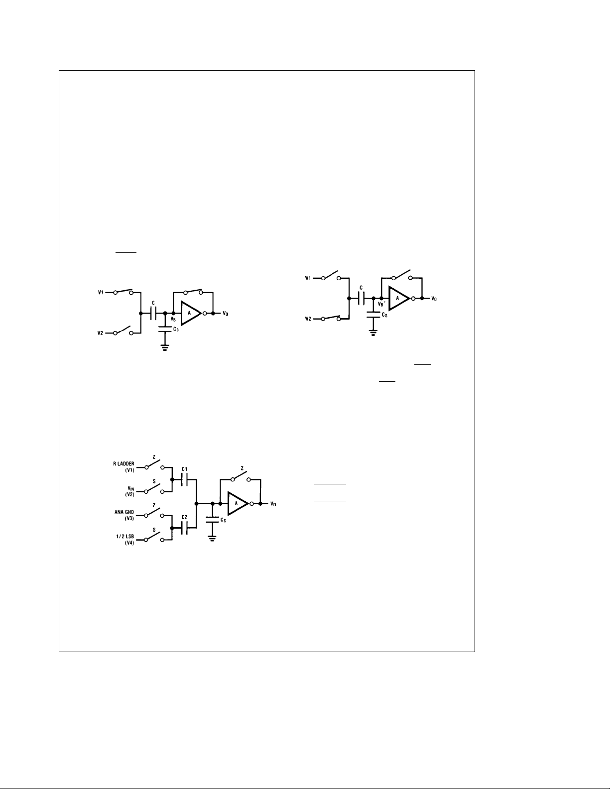
1.0 Functional Description (Continued)
1.2 THE SAMPLED-DATA COMPARATOR
Each comparator in the ADC0820 consists of a CMOS inverter with a capacitively coupled input (
switches connect the two comparator inputs to the input
capacitor (C) and also connect the inverter’s input and output. This device in effect now has one differential input pair.
A comparison requires two cycles, one for zeroing the comparator, and another for making the comparison.
In the first cycle, one input switch and the inverter’s feedback switch (
Figure 5a
) are closed. In this interval, C is
charged to the connected input (V1) less the inverter’s bias
voltage (V
ure 5b
, approximately 1.2V). In the second cycle (
B
), these two switches are opened and the other (V2)
input’s switch is closed. The input capacitor now subtracts
its stored voltage from the second input and the difference
is amplified by the inverter’s open loop gain. The inverter’s
input (V
V
and the output will go high or low depending on the sign of
V
b
B
b
Ê
B
) becomes
Ê
B
(V1bV2)
VB.
C
CaC
S
FIGURE 5a. Zeroing Phase
Figure 5
e
V
V
#
O
B
VonCeV1bV
#
e
C
stray input
#
S
node capacitor
e
V
inverter input
#
B
bias voltage
). Analog
Fig-
TL/H/5501– 12
B
FIGURE 5. Sampled-Data Comparator
The actual circuitry used in the ADC0820 is a simple but
important expansion of the basic comparator described
above. By adding a second capacitor and another set of
switches to the input (
Figure 6
), the scheme can be expanded to make dual differential comparisons. In this circuit, the
feedback switch and one input switch on each capacitor (Z
switches) are closed in the zeroing cycle. A comparison is
then made by connecting the second input on each capacitor and opening all of the other switches (S switches). The
change in voltage at the inverter’s input, as a result of the
change in charge on each input capacitor, will now depend
on both input signal differences.
1.3 ARCHITECTURE
In the ADC0820, one bank of 15 comparators is used in
each 4-bit flash A/D converter (
Figure 7
). The MS (most
significant) flash ADC also has one additional comparator to
detect input overrange. These two sets of comparators operate alternately, with one group in its zeroing cycle while
the other is comparing.
TL/H/5501– 13
(V2bV1)
[
CV2
S
C
CaC
S
b
]
CV1
b
e
V
V
#
Ê
B
B
b
A
e
V
#
Ê
O
CaC
V
is dependent on V2bV1
#
Ê
O
FIGURE 5b. Compare Phase
b
A
e
V
O
C1aC2aC
S
b
A
e
C1aC2aC
S
TL/H/5501– 14
FIGURE 6. ADC0820 Comparator (from MS Flash ADC)
8
[
C1(V2
[
DQ
C1
b
V1)aC2(V4bV3)
a
]
DQ
C2
]
Page 9

Detailed Block Diagram
FIGURE 7
9
TL/H/5501– 15
Page 10

1.0 Functional Description (Continued)
When a typical conversion is started, the WR
low. At this instant the MS comparators go from zeroing to
comparison mode (
Figure 8
). When WR is returned high after at least 600 ns, the output from the first set of comparators (the first flash) is decoded and latched. At this point the
two 4-bit converters change modes and the LS (least significant) flash ADC enters its compare cycle. No less than 600
ns later, the RD
line may be pulled low to latch the lower 4
data bits and finish the 8-bit conversion. When RD
the flash A/Ds change state once again in preparation for
the next conversion.
Figure 8
also outlines how the converter’s interface timing
relates to its analog input (V
measured while WR
is low. In RD mode, sampling occurs
during the first 800 ns of RD
). In WR-RD mode, VINis
IN
. Because of the input connections to the ADC0820’s LS and MS comparators, the converter has the ability to sample V
2.4), despite the fact that two separate 4-bit conversions are
IN
being done. More specifically, when WR
is in compare mode (connected to V
in zero mode (also connected to V
ADCs sample V
at the same time.
IN
IN
1.4 DIGITAL INTERFACE
The ADC0820 has two basic interface modes which are selected by strapping the MODE pin high or low.
RD Mode
With the MODE pin grounded, the converter is set to Read
mode. In this configuration, a complete conversion is done
by pulling RD
low until output data appears. An INT line is
provided which goes low at the end of the conversion as
well as a RDY output which can be used to signal a processor that the converter is busy or can also serve as a system
Transfer Acknowledge signal.
RD Mode (Pin 7 is Low)
line is brought
goes low,
at one instant (Section
is low the MS flash
), and the LS flash is
IN
). Therefore both flash
WR then RD Mode
With the MODE pin tied high, the A/D will be set up for the
WR-RD mode. Here, a conversion is started with the WR
input; however, there are two options for reading the output
data which relate to interface timing. If an interrupt driven
scheme is desired, the user can wait for INT
fore reading the conversion result (
cally go low 800 ns after WR
Figure B
’s rising edge. However, if a
to go low be-
). INT will typi-
shorter conversion time is desired, the processor need not
wait for INT
ure A
and can exercise a read after only 600 ns (
Fig-
). If this is done, INT will immediately go low and data
will appear at the outputs.
TL/H/5501– 17
FIGURE A. WR-RD Mode (Pin 7 is High and t
RD
k
tI)
TL/H/5501– 16
When in RD mode, the comparator phases are internally
triggered. At the falling edge of RD
, the MS flash converter
goes from zero to compare mode and the LS ADC’s comparators enter their zero cycle. After 800 ns, data from the
MS flash is latched and the LS flash ADC enters compare
mode. Following another 800 ns, the lower 4 bits are recovered.
FIGURE B. WR-RD Mode (Pin 7 is High and t
Stand-Alone
For stand-alone operation in WR-RD mode, CS
be tied low and a conversion can be started with WR
will be valid approximately 800 ns following WR
edge.
WR-RD Mode (Pin 7 is High) Stand-Alone Operation
10
TL/H/5501– 18
l
tI)
RD
and RD can
. Data
’s rising
TL/H/5501– 19
Page 11
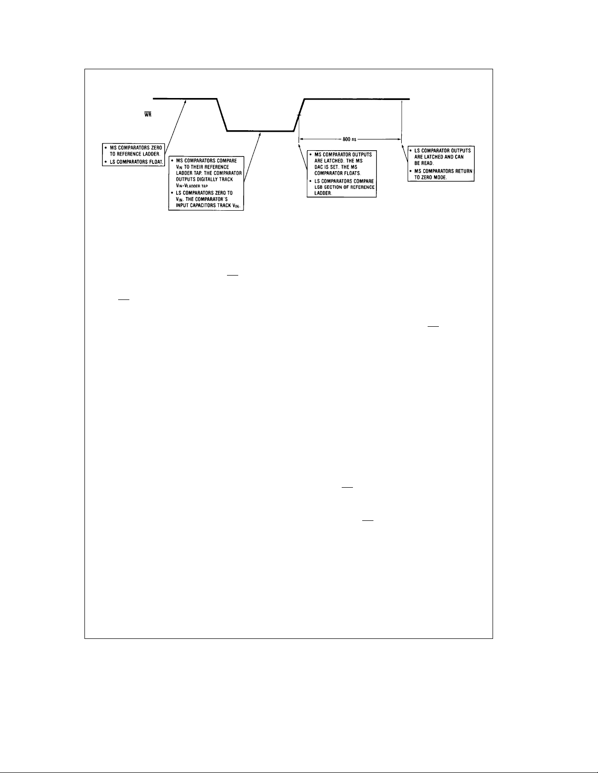
1.0 Functional Description (Continued)
Note: MS means most significant
LS means least significant
FIGURE 8. Operating Sequence (WR-RD Mode)
OTHER INTERFACE CONSIDERATIONS
In order to maintain conversion accuracy, WR
has a maximum width spec of 50 ms. When the MS flash ADC’s sampled-data comparators (Section 1.2) are in comparison
mode (WR
is low), the input capacitors (C,
Figure 6
) must
hold their charge. Switch leakage and inverter bias current
can cause errors if the comparator is left in this phase for
too long.
Since the MS flash ADC enters its zeroing phase at the end
of a conversion (Section 1.3), a new conversion cannot be
started until this phase is complete. The minimum spec for
this time (t
,
Figures 2, 3a, 3b,
P
and4) is 500 ns.
2.0 Analog Considerations
2.1 REFERENCE AND INPUT
The two V
and define the zero to full-scale input range of the A to D
converter. This allows the designer to easily vary the span
of the analog input since this range will be equivalent to the
voltage difference between V
V
REF(VREF
sitivity of the converter can be increased (i.e., if V
then 1 LSB
also facilitates ratiometric operation and in many cases the
chip power supply can be used for transducer power as well
as the V
This reference flexibility lets the input span not only be varied but also offset from zero. The voltage at V
the input level which produces a digital output of all zeroes.
Though V
affords nearly differential-input capability for most measurement applications.
tions that are possible.
inputs of the ADC0820 are fully differential
REF
(a) and VIN(b). By reducing
e
V
(a)bV
REF
e
7.8 mV). The input/reference arrangement
source.
REF
is not itself differential, the reference design
IN
IN
(b)) to less than 5V, the sen-
REF
Figure 9
shows some of the configura-
REF
e
REF
(b) sets
2V
TL/H/5501– 20
2.2 INPUT CURRENT
Due to the unique conversion techniques employed by the
ADC0820, the analog input behaves somewhat differently
than in conventional devices. The A/D’s sampled-data comparators take varying amounts of input current depending
on which cycle the conversion is in.
The equivalent input circuit of the ADC0820 is shown in
Figure 10a
mode), all input switches close, connecting V
1 pF capacitors. Although the two 4-bit flash circuits are not
both in their compare cycle at the same time, V
all input capacitors at once. This is because the MS flash
. When a conversion starts (WR low, WR-RD
to thirty-one
IN
still sees
IN
converter is connected to the input during its compare interval and the LS flash is connected to the input during its
zeroing phase (Section 1.3). In other words, the LS ADC
uses V
as its zero-phase input.
IN
The input capacitors must charge to the input voltage
through the on resistance of the analog switches (about 5
kX to 10 kX). In addition, about 12 pF of input stray capacitance must also be charged. For large source resistances,
the analog input can be modeled as an RC network as
shown in
Figure 10b
.AsRSincreases, it will take longer for
the input capacitance to charge.
In RD mode, the input switches are closed for approximately
800 ns at the start of the conversion. In WR-RD mode, the
time that the switches are closed to allow this charging is
the time that WR
is low. Since other factors force this time
to be at least 600 ns, input time constants of 100 ns can be
accommodated without special consideration. Typical total
input capacitance values of 45 pF allow R
without lengthening WR
to give VINmore time to settle.
to be 1.5 kX
S
11
Page 12

2.0 Analog Considerations (Continued)
External Reference 2.5V Full-Scale
Power Supply as Reference
Input Not Referred to GND
TL/H/5501– 21
FIGURE 9. Analog Input Options
FIGURE 10a
TL/H/5501– 24
2.3 INPUT FILTERING
It should be made clear that transients in the analog input
signal, caused by charging current flowing into V
degrade the A/D’s performance in most cases. In effect the
, will not
IN
ADC0820 does not ‘‘look’’ at the input when these transients occur. The comparators’ outputs are not latched
while WR
is low, so at least 600 ns will be provided to
charge the ADC’s input capacitance. It is therefore not necessary to filter out these transients by putting an external
cap on the V
terminal.
IN
2.4 INHERENT SAMPLE-HOLD
Another benefit of the ADC0820’s input mechanism is its
ability to measure a variety of high speed signals without the
help of an external sample-and-hold. In a conventional SAR
type converter, regardless of its speed, the input must remain at least (/2 LSB stable throughout the conversion process if full accuracy is to be maintained. Consequently, for
many high speed signals, this signal must be externally
sampled, and held stationary during the conversion.
TL/H/5501– 22
TL/H/5501– 23
TL/H/5501– 25
FIGURE 10b
Sampled-data comparators, by nature of their input switching, already accomplish this function to a large degree (Section 1.2). Although the conversion time for the ADC0820 is
1.5 ms, the time through which V
is much smaller. Since the MS flash ADC uses V
‘‘compare’’ input and the LS ADC uses V
input, the ADC0820 only ‘‘samples’’ V
(Sections 1.3 and 2.2). Even though the two flashes are not
must be 1/2 LSB stable
IN
IN
IN
as its ‘‘zero’’
IN
when WR is low
as its
done simultaneously, the analog signal is measured at one
instant. The value of V
rising edge of WR
approximately 100 ns after the
IN
(100 ns due to internal logic prop delay)
will be the measured value.
Input signals with slew rates typically below 100 mV/ms can
be converted without error. However, because of the input
time constants, and charge injection through the opened
comparator input switches, faster signals may cause errors.
Still, the ADC0820’s loss in accuracy for a given increase in
signal slope is far less than what would be witnessed in a
conventional successive approximation device. An SAR
type converter with a conversion time as fast as 1 ms would
still not be able to measure a 5V 1 kHz sine wave without
the aid of an external sample-and-hold. The ADC0820, with
no such help, can typically measure 5V, 7 kHz waveforms.
12
Page 13

3.0 Typical Applications
8-Bit Resolution Configuration
Telecom A/D Converter
9-Bit Resolution Configuration
TL/H/5501– 26
TL/H/5501– 27
Multiple Input Channels
e
V
3 kHz maxg4V
#
IN
No track-and-hold needed
#
Low power consumption
#
P
TL/H/5501– 28
TL/H/5501– 29
13
Page 14

3.0 Typical Applications (Continued)
8-Bit 2-Quadrant Analog Multiplier
Fast Infinite Sample-and-Hold
TL/H/5501– 30
TL/H/5501– 31
14
Page 15
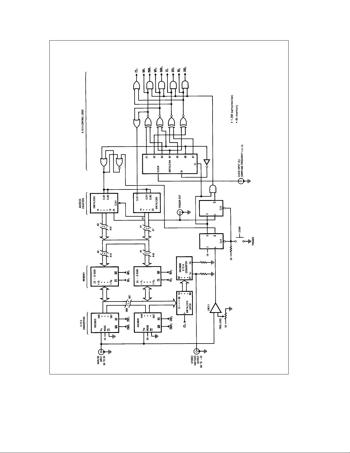
3.0 Typical Applications (Continued)
TL/H/5501– 32
Digital Waveform Recorder
15
Page 16

Ordering Information
Part Number
ADC0820BCV V20AÐMolded Chip 0§Ctoa70§C
ADC0820BCWM
ADC0820BCN N20AÐMolded DIP 0
ADC0820CCJ J20AÐCerdip
ADC0820CCMSA MSA20Ð Shrink Small 0
ADC0820CCV
ADC0820CCWM M20BÐWide Body Small 0
ADC0820CIWM M20BÐWide Body Small
ADC0820CCN N20AÐMolded DIP 0
Total
Unadjusted Error Range
g
(/2 LSB M20BÐWide Body Small 0§Ctoa70§C
g
1 LSB V20AÐMolded Chip 0§Ctoa70§C
Package
Carrier
Outline
Outline
Package
Carrier
Outline
Outline
Temperature
Ctoa70§C
§
b
40§Ctoa85§C
Ctoa70§C
§
Ctoa70§C
§
b
40§Ctoa85§C
Ctoa70§C
§
16
Page 17

17
Page 18

Physical Dimensions inches (millimeters)
Hermetic Dual-In-Line Package (J)
Order Number ADC0820CCJ
NS Package Number J20A
Order Number ADC0820BCWM, ADC0820CCWM or ADC0820CIWM
SO Package (M)
NS Package Number M20B
18
Page 19

Physical Dimensions inches (millimeters) (Continued)
Shrink Small Outline Package (SSOP)
Order Number ADC0820CCMSA
NS Package Number MSA20
Molded Dual-In-Line Package (N)
Order Number ADC0820BCN or ADC0820CCN
NS Package Number N20A
19
Page 20

Physical Dimensions inches (millimeters) (Continued)
Molded Chip Carrier Package (V)
Order Number ADC0820BCV or ADC0820CCV
NS Package Number V20A
LIFE SUPPORT POLICY
NATIONAL’S PRODUCTS ARE NOT AUTHORIZED FOR USE AS CRITICAL COMPONENTS IN LIFE SUPPORT
DEVICES OR SYSTEMS WITHOUT THE EXPRESS WRITTEN APPROVAL OF THE PRESIDENT OF NATIONAL
SEMICONDUCTOR CORPORATION. As used herein:
1. Life support devices or systems are devices or 2. A critical component is any component of a life
systems which, (a) are intended for surgical implant support device or system whose failure to perform can
into the body, or (b) support or sustain life, and whose be reasonably expected to cause the failure of the life
failure to perform, when properly used in accordance support device or system, or to affect its safety or
with instructions for use provided in the labeling, can effectiveness.
be reasonably expected to result in a significant injury
ADC0820 8-Bit High Speed mP Compatible A/D Converter with Track/Hold Function
to the user.
National Semiconductor National Semiconductor National Semiconductor National Semiconductor
Corporation Europe Hong Kong Ltd. Japan Ltd.
1111 West Bardin Road Fax: (
Arlington, TX 76017 Email: cnjwge@tevm2.nsc.com Ocean Centre, 5 Canton Rd. Fax: 81-043-299-2408
Tel: 1(800) 272-9959 Deutsch Tel: (
Fax: 1(800) 737-7018 English Tel: (
National does not assume any responsibility for use of any circuitry described, no circuit patent licenses are implied and National reserves the right at any time without notice to change said circuitry and specifications.
Fran3ais Tel: (
Italiano Tel: (
a
49) 0-180-530 85 86 13th Floor, Straight Block, Tel: 81-043-299-2309
a
49) 0-180-530 85 85 Tsimshatsui, Kowloon
a
49) 0-180-532 78 32 Hong Kong
a
49) 0-180-532 93 58 Tel: (852) 2737-1600
a
49) 0-180-534 16 80 Fax: (852) 2736-9960
 Loading...