

Page 1
ADC08161
500 ns A/D Converter with S/H Function and 2.5V
Bandgap Reference
ADC08161 500 ns A/D Converter with S/H Function and 2.5V Bandgap Reference
November 1995
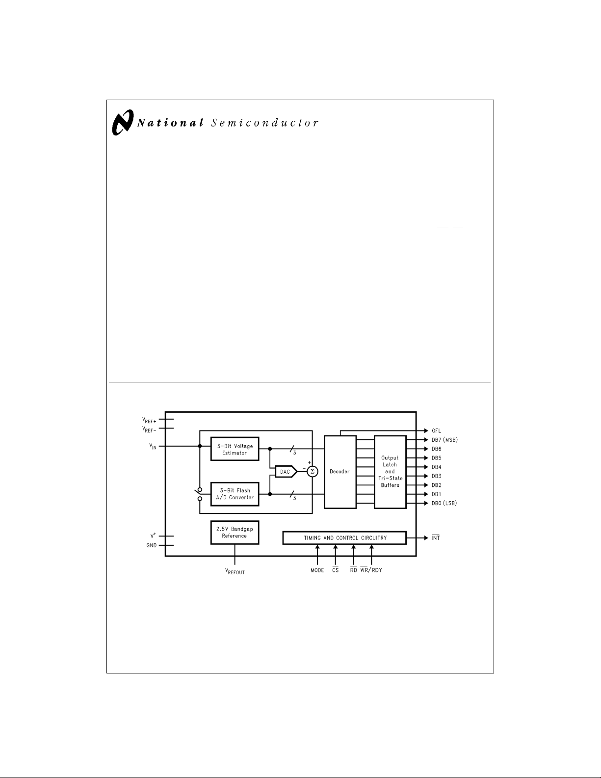
General Description
Using a patented multi-step A/D conversion technique, the
8-bit ADC08161 CMOS A/D converter offers 500 ns conversion time, internal sample-and-hold (S/H), a 2.5V bandgap
reference, and dissipates only 100 mW of power. The
ADC08161 performs an 8-bit conversion with a 2-bit voltage
estimator that generates the 2 MSBs and two low-resolution
(3-bit) flashes that generate the 6 LBSs.
Input signals are tracked and held by the input sampling circuitry, eliminating the need for an external sample-and-hold.
The ADC08161 can perform accurate conversions of
full-scale input signals at frequencies from DC to typically
more than 300 kHz (full power bandwidth) without the need
of an external sample-and-hold (S/H).
For ease of interface to microprocessors, this part has been
designed to appear as a memory location or I/O port without
the need for external interfacing logic.
Block Diagram
Key Specifications
n Resolution: 8 Bits
n Conversion time (t
n Full power bandwidth: 300 kHz (typ)
n Throughput rate: 1.5 MHz min
n Power dissipation: 100 mW max
n Total unadjusted error:
): 560 ns max (WR -RD Mode)
CONV
1
±
⁄2LSB and±1 LSB max
Features
n No external clock required
n Analog input voltage range from GND to V
n 2.5V bandgap reference
Applications
n Mobile telecommunications
n Hard-disk drives
n Instrumentation
n High-speed data acquisition systems
+
DS011149-1
TRI-STATE®is a registeredtrademark of National Semiconductor Corporation.
© 1997 National Semiconductor Corporation DS011149 www.national.com
Page 2
Absolute Maximum Ratings (Notes 1,
2)
If Military/Aerospace specified devices are required,
please contact the National Semiconductor Sales Office/
Distributors for availability and specifications.
Supply Voltage (V
Logic Control Inputs −0.3V to V
Voltage at Other Inputs and Outputs −0.3V to V
Input Current at Any Pin (Note 3) 5 mA
Package Input Current (Note 3) 20 mA
Power Dissipation (Note 4)
N Package 875 mW
WM Package 875 mW
Lead Temperature (Note 5)
N Package (Soldering, 10 sec.) +260˚C
+
)6V
+
+ 0.3V
+
+ 0.3V
WM Package
(Vapor Phase, 60 sec.) +215˚C
WM Package (Infrared, 15 sec.) +220˚C
Storage Temperature −65˚C to +150˚C
ESD Susceptibility (Note 6) 750V
Operating Ratings (Note 1) (Note 2)
Temperature Range T
ADC08161BIN, −40˚C ≤ TA≤ 85˚C
ADC08161CIN,
ADC08161BIWM,
ADC08161CIWM
Supply Voltage, (V
+
) 4.5V to 5.5V
MIN
≤ TA≤ T
MAX
Converter Characteristics
The following specifications apply for RD Mode, V
face limits apply for T
=
=
T
A
to T
T
J
MIN
+
=
; all other limits T
MAX
5V, V
REF+
=
5V, and V
=
T
A
=
GND unless otherwise specified. Bold-
REF−
=
25˚C.
J
Symbol Parameter Conditions Typical Limits Units
(Note 7) (Note 8) (Limit)
INL Integral Non Linearity V
REF
=
5V
1
±
⁄
2
LSB (max)
ADC08161BIN, BIWM
±
1 LSB (max)
1
±
⁄
2
LSB (max)
TUE Total Unadjusted Error (Note 9) V
ADC08161CIN, CIWM
=
5V
REF
ADC08161BIN, BIWM
±
1 LSB (max)
±
1 LSB (max)
±
1 LSB (max)
INL Integral Non Linearity V
TUE Total Unadjusted Error V
ADC08161CIN, CIWM,
=
2.5V, All Suffixes
REF
=
2.5V
REF
ADC08161, All Suffixes
Missing Codes V
=
5V 0 Bits (max)
REF
=
V
2.5V 0 Bits (max)
REF
Reference Input Resistance 700 500 Ω (min)
700 1250 Ω (max)
V
REF+
V
REF−
V
IN
Positive Reference Input Voltage V
REF−
V
+
V (min)
V (max)
Negative Reference GND V (min)
Input Voltage V
REF+
V (max)
Analog (Note 10) GND − 0.1 V (min)
Input Voltage V
+
+ 0.1 V (max)
On-Channel Input Current On Channel Input=5V,
Off Channel Input=0V −0.4 −20 µA (max)
(Note 11)
On Channel Input=0V,
Off Channel Input=5V −0.4 −20 µA (max)
(Note 11)
+
=
PSS Power Supply Sensitivity V
±
5%,
5V
=
V
4.75V
REF
±
1/16
1
±
⁄
2
LSB (max)
All Codes Tested
Effective Bits V
Full-Power Bandwidth V
=
4.85 V
IN
=
f
20 Hz to 20 kHz
IN
=
4.85 V
IN
p-p
p-p
7.8 Bits
300 kHz
www.national.com 2
Page 3
Converter Characteristics (Continued)
+
The following specifications apply for RD Mode, V
face limits apply for T
=
=
T
A
to T
T
J
MIN
=
; all other limits T
MAX
5V, V
Symbol Parameter Conditions Typical Limits Units
THD Total Harmonic Distortion V
S/N Signal-to-Noise Ratio V
IMD Intermodulation Distortion V
C
VIN
Analog Input Capacitance 25 pF
=
IN
=
f
IN
=
IN
=
f
IN
=
IN
=
f
IN
=
5V, and V
REF+
=
T
A
J
4.85 V
p-p
20 Hz to 20 kHz
4.85 V
p-p
20 Hz to 20 kHz
4.85 V
p-p
20 Hz to 20 kHz
=
25˚C.
=
GND unless otherwise specified. Bold-
REF−
(Note 7) (Note 8) (Limit)
0.5
50 dB
50 dB
%
AC Electrical Characteristics
The following specifications apply for V
limits apply for T
=
=
T
A
T
J
MIN
to T
+
MAX
=
=
5V, t
; all other limits T
=
t
r
f
10 ns, V
=
A
T
REF+
J
=
Symbol Parameter Conditions
t
WR
t
RD
Write Time Mode Pin to V
(
Figures 2, 3, 4
Read Time (Time from Rising Edge Mode Pin to V+,(
+
)
Figure 2
of WR to Falling Edge of RD )
t
RDW
t
CONV
t
CRD
t
ACCO
t
ACC1
t
ACC2
t
1H,t0H
RD Width Mode Pin to GND (
WR -RD Mode Conversion Time Mode Pin to V+,(
(t
WR+tRD+tACC1
)
Figure 2
RD Mode Conversion Time Mode Pin to GND, (
Access Time (Delay from Falling CL≤ 100 pF, Mode Pin to GND 640 900 ns (max)
Edge of RD to Output Valid)
(
Figure 1
)
Access Time (Delay from CL≤ 10 pF 45 ns
Falling Edge of RD
to Output Valid) Mode Pin to V
=
C
100 pF 50 110 ns (max)
L
(
Figure 2
+
,tRD≤ t
)
Access Time (Delay from CL≤ 10 pF 25 ns
Falling Edge of RD
to Output Valid) t
TRI-STATE®Control R
(Delay from Rising Edge (
=
C
100 pF 30 55 ns (max)
L
>
t
=
L
,
INTL
3kΩ,C
)
=
10 pF
L
RD
(
Figures 3, 5
Figures 1, 2, 3, 4, 5
of RD to HI-Z State)
t
t
t
INTL
INTH
INTH
Delay from Rising Edge of Mode Pin=V+,C
WR to Falling Edge of INT
Delay from Rising Edge of C
RD to Rising Edge of INT
Delay from Rising Edge of C
(
Figures 3, 4
L
(
Figures 1, 2, 3, 5
L
)
=
50 pF, 50 95 ns (max)
=
50 pF, (
Figure 4
L
)
WR to Rising Edge of INT
t
RDY
Delay from CS to RDY Mode Pin=0V, C
=
R
L
3kΩ,(
Figure 1
L
=
25˚C.
5V, V
=
0V unless otherwise specified. Boldface
REF−
ADC08161BIN, ADC08161CIN,
ADC08161BIWM,
ADC08161CIWM
Typical Limit
Units
(Limit)
(Note 7) (Note 8)
100 100 ns (min)
) 350 350 ns (min)
Figure 5
) 200 250 ns (min)
400 400 ns (max)
) 500 560 ns (max)
Figure 1
) 655 900 ns (max)
INTL
)3060 ns (max)
=
50 pF 520 690 ns (max)
)4595 ns (max)
=
50 pF, 25 45 ns (max)
)
3 www.national.com
Page 4
AC Electrical Characteristics (Continued)
+
=
=
The following specifications apply for V
limits apply for T
=
=
T
A
to T
T
J
MIN
5V, t
; all other limits T
MAX
Symbol Parameter Conditions
t
ID
Delay from INT R
to Output Valid (
t
RI
t
N
Delay from RD to INT Mode Pin=V+,tRD≤ t
Time between End of RD (
and Start of New Conversion
t
CSS
t
CSH
CS Setup Time (
CS Hold Time (
=
t
10 ns, V
r
f
=
T
A
=
3kΩ,C
L
Figure 4
(
Figure 2
L
)
)
Figures 1, 2, 3, 4, 5
Figures 1, 2, 3, 4, 5
Figures 1, 2, 3, 4, 5
REF+
=
25˚C.
J
=
100 pF 0 15 ns (max)
=
5V, V
=
0V unless otherwise specified. Boldface
REF−
ADC08161BIN, ADC08161CIN,
ADC08161BIWM,
ADC08161CIWM
Typical Limit
Units
(Limit)
(Note 7) (Note 8)
INTL
60 115 ns (max)
)5050 ns (min)
)00ns (max)
)00ns (max)
DC Electrical Characteristics
The following specifications apply for V
all other limits T
Symbol Parameter Conditions ADC08161BIN, ADC08161CIN, Units
=
=
T
25˚C.
A
J
+
=
5V unless otherwise specified. Boldface limits apply for T
ADC08161BIWM, ADC08161CIWM
=
=
T
A
to T
T
J
MIN
MAX
(Limit)
Typical Limit
(Note 7) (Note 8)
+
Logic “1” Input Voltage V
V
IH
=
5.5 V
CS , WR , RD , A0, A1, A2 Pins
2.0 V (min)
Mode Pin 3.5
+
V
Logic “0” Input Voltage V
IL
=
4.5V
CS , WR , RD , A0, A1, A2 Pins
0.8 V (max)
Mode Pin 1.5
I
Logic “1” Input Current V
IH
=
5V
H
CS , RD , A0, A1, A2 Pins
WR Pin
0.005 1
0.1 3 µA (max)
Mode Pin 50 200
I
Logic “0” Input Current V
IL
=
0V
L
CS , RD , WR , A0, A1, A2
Mode Pins −0.005 −2 µA (max)
+
V
Logic “1” Output Voltage V
OH
=
4.75V
=
I
−360 µA 2.4 V (min)
OUT
DB0–DB7, OFL , INT
=
I
−10 µA 4.5 V (min)
OUT
DB0–DB7, OFL , INT
+
V
Logic “0” Output Voltage V
OL
=
4.75V
=
I
1.6 mA 0.4 V (max)
OUT
DB0–DB7, OFL , INT , RDY
I
TRI-STATE Output Current V
O
=
5.0V 0.1 3 µA (max)
OUT
DB0–DB7, RDY
=
V
0V −0.1 −3 µA (max)
OUT
DB0–DB7, RDY
I
Output Source Current V
SOURCE
=
0V −26 −6 mA (min)
OUT
DB0–DB7, OFL , INT
;
www.national.com 4
Page 5
DC Electrical Characteristics (Continued)
+
The following specifications apply for V
all other limits T
=
=
T
25˚C.
A
J
=
5V unless otherwise specified. Boldface limits apply for T
Symbol Parameter Conditions ADC08161BIN, ADC08161CIN, Units
ADC08161BIWM, ADC08161CIWM
Typical Limit
(Note 7) (Note 8)
I
Output Sink Current V
SINK
=
5V 24 7 mA (min)
OUT
DB0–DB7, OFL , INT , RDY
I
C
C
Supply Current CS=WR=RD=0 11.5 20 mA (max)
C
Logic Output Capacitance 5 pF
OUT
Logic Input Capacitance 5 pF
IN
=
=
T
A
to T
T
J
MIN
MAX
(Limit)
;
Bandgap Reference Electrical Characteristics
The following specifications apply for V
=
limits T
=
T
25˚C.
A
J
+
=
5V unless otherwise specified. Boldface limits apply for T
MIN
to T
MAX
; all other
Symbol Parameter Conditions Typical Limits Units
(Note 7) (Note 8) (Limit)
V
REFOUT
Internal Reference Output Voltage “B” Grade 2.5 2.5±1.5
“C” Grade 2.5
∆V
/∆T Internal Reference Temperature 40 ppm/˚C
REF
%
V (max)
±
%
2.0
Coefficient
∆V
/∆ILInternal Reference Load Sourcing (0 ≤ IL≤ +10 mA) 0.01 0.1
REF
%
/mA (max)
Regulation
Line Regulation 4.75V ≤ V
I
∆V
SC
REF/∆t
Short Circuit Current V
Long Term Stability 200 ppm/kHr
Start-Up Time V
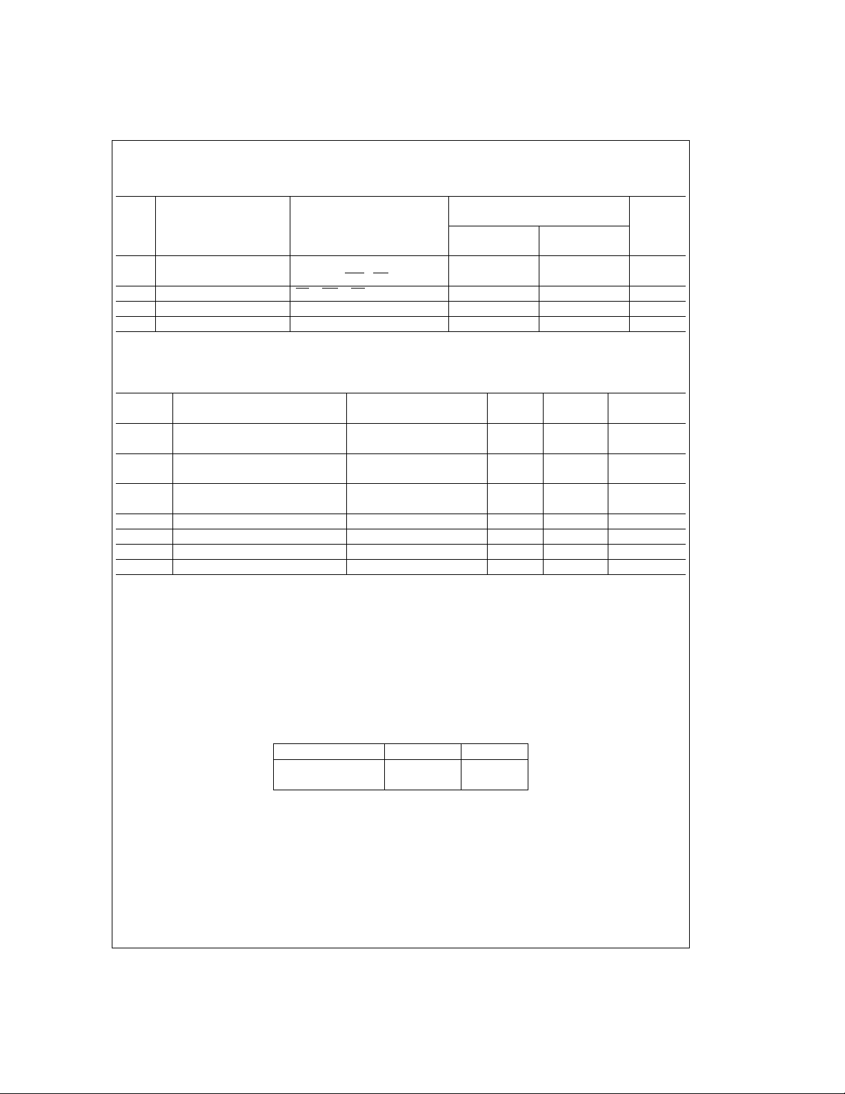
Note 1: Absolute Maximum Ratings indicate limits beyond which damage to the device may occur. DC and AC electrical specifications do not apply when operating
the device beyond its specified operating ratings. Operating Ratings indicate conditions for which the device is functional, but do not guarantee performance limits.
For guaranteed specifications and test conditions, see the Electrical Characteristics. The guaranteed specificationsapply only for the test conditions listed. Some performance characteristics may degrade when the device is not operated under the listed test conditions.
Note 2: All voltages are measured with respect to the GND pin, unless otherwise specified.
Note 3: When the input voltage (V
limited to 5 mA or less. The 20 mA package input current specification limits the number of pins that can exceed the power supply boundaries witha5mAcurrent
limit to four.
Note 4: The power dissipation of this device under normal operation should never exceed 875 mW (Quiescent Power Dissipation + TTLLoads on the digital outputs).
Caution should be taken not to exceed absolute maximum power rating when the device is operating in a severe fault condition (e.g., when any input or output exceeds the power supply). The maximum power dissipation must be derated at elevated temperatures and is dictated by T
(package junction to ambient thermal resistance), and TA(ambient temperature). The maximum allowable power dissipation at any temperature is PD
−TA)/θJAor the number given in the Absolute Maximum Ratings, whichever is lower. The table below details T
of the ADC08161.
) at any pin exceeds the power supply voltage (V
IN
Part Number T
+
≤ 5.25V 0.5 6.0 mV (max)
=
0V 35 mA (max)
REV
+
:0V→5V, C
=
220 µF 40 ms
L
IN
JMAX
<
GND or V
>
V+), the absolute value of the current at that pin should be
IN
(maximum junction temperature), θ
JMAX
and θJAfor the various packages and versions
JMAX
θ
JA
max
=
(T
ADC08161B/CIN 105 51
ADC08161B/CIWM 105 85
Note 5: See AN-450 “Surface Mounting Methods and Their Effect on Product Reliability” for other methods of soldering surface mount devices.
Note 6: Human body model, 100 pF discharged through a 1.5 kΩ resistor.
Note 7: Typicals are at 25˚C and represent most likely parametric norm.
Note 8: Limits are guaranteed to National’s AOQL (Average Output Quality Level).
Note 9: Total unadjusted error includes offset, full-scale, and linearity errors.
Note 10: Two on-chip diodes are tied to each analog input and are reversed biased during normal operation. One is connected to V
GND. They will become forward biased and conduct when an analog input voltage is equal to or greater than one diode drop above V
caution should be exercised when testing with V
peratures. This can create conversion errors for analog signals near full-scale. The specification allows 50 mV forward bias on either diode; e.g., the output code will
be correct as long as the analog input signal does not exceed the supply voltage by more than 50 mV. Exceeding this range on an unselected channel will corrupt
the reading of a selected channel. An absolute analog input signal voltage range of 0V ≤ V
+
is 4.950V over temperature variations, initial tolerance, and loading.
plied to V
+
=
4.5V.Analog inputs with magnitudes equal to 5V can cause an input diode to conduct, especially at elevated tem-
≤ 5V can be achieved by ensuring that the minimum supply voltage ap-
IN
+
and the other is connected to
+
or below GND. Therefore,
JMAX
JA
5 www.national.com
Page 6

Bandgap Reference Electrical Characteristics (Continued)
Note 11: Off-channel leakage current is measured on the on-channel selection.
TRI-STATE Test Circuit and Waveforms
t
1H
DS011149-2
t
0H
DS011149-3
=
t
10 ns
r
=
t
10 ns
r
t1H,C
t0H,C
=
10 pF
L
DS011149-4
=
10 pF
L
DS011149-5
FIGURE 1. RD Mode (Mode Pin is Low)
www.national.com 6
DS011149-6
Page 7

TRI-STATE Test Circuit and Waveforms (Continued)
FIGURE 2. WR -RD Mode with tRD≤ t
(Mode Pin is High)
INTL
DS011149-7
FIGURE 3. WR -RD Mode with t
DS011149-8
>
t
RD
7 www.national.com
(Mode Pin is High)
INTL
Page 8
TRI-STATE Test Circuit and Waveforms (Continued)
FIGURE 4. WR -RD Mode Reduced Interface System Connection with CS=RD=0 (Mode Pin is High)
DS011149-9
FIGURE 5. RD Mode (Pipeline Operation); t
(Mode Pin is Low)
Typical Performance Characteristics
t
vs Temperature
CRD
DS011149-23
www.national.com 8
Linearity Error vs
Reference Voltage
must be between 200 ns and 400 ns.
RDW
Offset Error vs
Reference Voltage
DS011149-24
DS011149-10
DS011149-25
Page 9

Typical Performance Characteristics (Continued)
Supply Current vs
Temperature
DS011149-26
Reference Output Voltage vs
Temperature
DS011149-27
Output Current vs
Temperature
DS011149-29
Logic Threshold vs
Temperature
DS011149-28
Connection Diagram
Dual-In-Line and Wide-Body
See NS Package Number N20A or M20A
Ordering Information
Industrial (−40˚C ≤ TA≤ 85˚C) Package
ADC08161BIN, ADC08161CIN N20A
ADC08161BIWM, ADC08161CIWM M20B
Small-Outline Packages
Pin Description
V
IN
DB0–DB7 TRI-STATE data outputs — bit 0 (LSB) through
9 www.national.com
DS011149-14
This is the analog input. The input range is
GND–50 mV ≤ V
≤ V++50mV.
INPUT
bit 7 (MSB).
Page 10

Pin Description (Continued)
WR /RDY
MODE Mode: Mode (RD or WR -RD ) selection input–
RD
INT
WR -RD Mode (Logic high applied to MODE
pin)
WR : With CS low, the conversion is started on
the rising edge of WR . The digital result will be
strobed into the output latch at the end of conversion (
Figures 2, 3, 4
).
RD Mode (Logic low applied to MODE pin)
RDY: This is an open drain output (no internal
pull-up device). RDY will go low after the falling
edge of CS and returns high at the end of conversion.
This pin is pulled to a logic low through an internal 50 µA current sink when left unconnected.
RD Mode is selected if the MODE pin is left unconnected or externally forced low. A complete
conversion is accomplished by pulling RD low
until output data appears.
WR -RD Mode is selected when a high is applied to the MODE pin. A conversion starts with
the WR signal’s rising edge and then using RD
to access the data.
WR -RD Mode (logic high on the MODE pin)
This is the active low Read input. With a logic
low applied to the CS pin, the TRI-STATE data
outputs (DB0–DB7) will be activated when RD
goes low (
Figures 2, 3, 4
).
RD Mode (logic low on the MODE pin)
With CS low, a conversion starts on the
falling edge of RD . Output data appears
on DB0–DB7 at the end of conversion
(
Figures 1, 5
).
This is an active low output that indicates
that a conversion is complete and the data
is in the output latch. INT is reset by the
rising edge of RD .
GND This is the power supply ground pin. The
ground pin should be connected to a
“clean” ground reference point.
V
REF−,VREF+
These are the reference voltage inputs.
They may be placed at any voltage between GND − 50 mV and V
V
must be greater than V
REF+
an input voltage equal to V
an output code of 0, and an input voltage
greater than V
output code of 255.
For the ADC08161 an input voltage that
exceeds V
REF+
+
by more than 100 mV or is be-
+
+50mV,but
. Ideally,
REF−
produces
REF−
− 1.5 LSB produces an
low GND by more than 100 mV will create
conversion errors.
CS
This is the active low Chip Select input. A
logic low signal applied to this input pin enables the RD and WR inputs. Internally,
the CS signal is ORed with RD and WR
signals.
OFL
Overflow Output. If the analog input is
higher than V
end of conversion. It can be used when
, OFL will be low at the
REF+
cascading two ADC08161s to achieve
higher resolution (9 bits). This output is always active and does not go into
TRI-STATE as DB0–DB7 do. When OFL
is set, all data outputs remain high when
+
V
the ADC08061’s output data is read.
Positive powersupply voltage input. Nomi-
nal operating supply voltage is +5V. The
supply pin should be bypassed with a 10
µF bead tantalum in parallel with a 0.1 ceramic capacitor. Lead length should be as
short as possible.
V
REFOUT
The internal bandgap reference’s 2.5V
output is available on this pin. Use a 220
µF bypass capacitor between this pin and
analog ground.
www.national.com 10
Page 11

Application Information
FIGURE 6. Block Diagram of the ADC08161 Multi-Step Flash Architecture
1.0 FUNCTIONAL DESCRIPTION
The ADC08161 performs an 8-bit analog-to-digital conversion using a multi-step flash technique. The first flash generates the five most significant bits (MSBs) and the second
flash generates the three least significant bits (LSBs).
6
shows the major functional blocks of the ADC08161
multi-step flash converter. It consists of an over-encoded
1
2
⁄2-bit Voltage Estimator, an internal DAC with two different
Figure
voltage spans, a 3-bit half-flash converter and a comparator
multiplexer.
The resistor string near the center of the block diagram in
Figure 6
forms the internal main DAC. Each of the eight resistors at the bottom of the string is equal to 1/256 of the total
string resistance. These resistors form the LSB Ladder and
have a voltage drop of 1/256 of the total reference voltage
(V
REF+−VREF−
up the MSB Ladder . They are made up of eight groups of
four resistors connected in series. Each MSB Ladder section
1
has
⁄8of the total reference voltage across it. Within a given
MSB Ladder section, each of the MSB resistors has 8/256,
1
or
⁄32 of the total reference voltage across it. Tap points are
) across them. The remaining resistors make
found between all of the resistors in both the MSB and LSB
DS011149-17
Ladders. Through the Comparator Multiplexer these tap
points can be connected, in groups of eight,to the eight comparators shown at the right of
Figure 6
. This function provides the necessary reference voltages to the comparators
during each flash conversion.
The six comparators, seven-resistor string (estimator DAC),
and Estimator Decoder at the left of
Figure 6
form the Voltage Estimator. The estimator DAC connected between
V
and V
REF+
six Voltage Estimator comparators. These comparators per-
generates the reference voltages for the
REF−
form a very low resolution A/D conversion to obtain an “estimate” of the input voltage. This estimate is then used to control the Comparator Multiplexer, connecting the appropriate
MSB Ladder section to the eight flash comparators. Only 14
comparators, six in the Voltage Estimator and eight in the
flash converter, are needed to achieve the full eight-bit resolution, instead of 32 comparators that would be needed by
traditional half-flash methods.
A conversion begins with the Voltage Estimator comparing
the analog input signal against the six tapvoltages on the estimator DAC. The estimator decoder then selects one of the
groups of tap points along the MSB Ladder. These eight tap
11 www.national.com
Page 12

Application Information (Continued)
points are then connected to the eight flash comparators.
For example, if the analog input signal applied to V
tween 0 and 3/16 of V
mator decoder instructs the comparator multiplexer to select
REF(VREF
=
V
REF+−VREF−
the eight tap points between 8/256 and 2/8 of V
nects them to the eight flash comparators. The first flash
conversion is now performed, producing the five MSBs of
data.
The remaining three LSBs are generated next using the
same eight comparators that were used for the first flash
conversion.As determined by the results of the MSB flash, a
voltage from the MSB Ladder equivalent to the magnitude of
the five MSBs is subtracted from the analog input voltage as
the upper switch is moved from position one to position two.
The resulting remainder voltage is applied to the eight flash
comparators and, with the lower switch in position two, compared with the eight tap points from the LSB Ladder.
By using the same eight comparators for both flash conversions, the number of comparators needed by the multi-step
converter is significantly reduced when compared to standard half-flash techniques.
Voltage Estimator errors as large as 1/16 of V
will be corrected since the flash comparators are connected
to ladder voltages that extend beyond the range specified by
the Voltage Estimator. For example, if 7/16 V
9/16 V
tap points below 9/16 V
decoded by the estimator decoder to “10”. The eight flash
comparators will be placed at the MSB Ladder tap points between
each side of the Voltage Estimator’s span will automatically
correct an error of up to 16 LSBs (16 LSBs=312.5 mV for
V
REF
input voltage is between
Voltage Estimator’s output code will be corrected by sub-
the Voltage Estimator’s comparators tied to the
REF
3
⁄8V
and5⁄8V
REF
=
5V). If the first flash conversion determines that the
will output “1”s (000111). This is
REF
. The overlap of 1/16 V
REF
3
⁄8V
and 4/8 V
REF
REF
tracting “1”. This results in a corrected value of “01”. If the
first flash conversion determines that the input voltage is between 8/16 V
tor’s output code remains unchanged.
− LSB/2 and5⁄8V
REF
, the Voltage Estima-
REF
After correction, the 2-bit data from both the Voltage Estimator and the first flash conversion are decoded to produce the
five MSBs. Decoding is similar to that of a 5-bit flash converter since there are 32 tap points on the MSB Ladder.
However, 31 comparators are not needed since the Voltage
Estimator places the eight comparators along the MSB Ladder where reference tap voltages are present that fall above
and below the magnitude of V
needed outside this selected range. If a comparator’s output
. Comparators are not
IN
is a “0”, all comparators above it will also have outputs of “0”
and if a comparator’s output is a “1”, all comparators below it
will also have outputs of “1”.
2.0 DIGITAL INTERFACE
TheADC08161 has two basic interface modes which are selected by connecting the MODE pin to a logic high or low.
2.1 RD Mode
With alogic low applied to the MODE pin, the converter is set
to Read mode. In this configuration (
Figure 1
conversion is done by pulling RD low, and holding low, until
the conversion is complete and output data appears. This
typically takes 655 ns. The INT (interrupt) line goes low at
the end of conversion. A typical delay of 50 ns is needed be-
is be-
IN
), the esti-
and con-
REF
(16 LSBs)
REF
<
V
REF
IN
REF
− LSB/2, the
), a complete
on
tween the rising edge of CS (after the end of a conversion)
and the start of the next conversion (by pulling RD low). The
RDY output goes low after the falling edge of CS and goes
high at the end-of-conversion. It can be used to signal a processor that the converter is busy or serve as a system Transfer Acknowledge signal.
2.2 RD Mode Pipelined Operation
Applications that require shorter RD pulse widths than those
used in the Read mode as described above can be achieved
by setting RD ’s width between 200 ns–400 ns (
RD pulse widths outside this range will create conversion linearity errors. These errors are caused by exercising internal
interface logic circuitry using CS and/or RD during a conversion.
When RD goes low, a conversion is initiated and the data
from the previous conversion is available on the DB0–DB7
outputs. Reading DB0–DB7 for the first two times after
power-up produces random data. The data will be valid during the third RD pulse that occurs after the first conversion.
2.3 WR -RD (WR then RD ) Mode
The ADC08161 is in the WR -RD mode with the MODE pin
tied high. A conversion starts on the rising edge of the WR
signal. There are two options for reading the output data
which relate to interface timing. If an interrupt-driven scheme
is desired, the user can wait for the INT output to go low be-
<
fore reading the conversion result (
Figure 3
will go low 690 ns, maximum, after WR’s rising edge. However, if a shorter conversion time is desired, the processor
need not wait for INT and can exercise a read after only 350
ns (
Figure 2
). If RD is pulled low before INT goes low, INT
will immediately go low and data will appear at the outputs.
This is the fastest operating mode (t
sion time, including data access time, of 560 ns. Allowing
RD
100 ns for reading the conversion data and the delay between conversions gives a total throughput time of 660 ns
(throughput rate of 1.5 MHz).
2.4 WR -RD Mode with Reduced Interface System
Connection
CS and RD can be tied low, using only WR to control the
start of conversion for applications that require reduced digital interface while operating in the WR -RD mode (
Data will be valid approximately 705 ns following WR’s rising
edge.
3.0 REFERENCE INPUTS
The ADC08161’s two V
define the zero to full-scale input range of the A to D con-
inputs are fully differential and
REF
verter. This allows the designer to vary the span of the analog input since this range will be equivalent to the voltage difference between V
outputs that minimum output voltages above GND can also
be compensated by connecting V
equal to this minimum voltage. By reducing V
V
REF+–VREF−
can be increased (i.e., if V
) to less than 5V,the sensitivity of the converter
The reference arrangement also facilitates ratiometric opera-
REF+
and V
. Transducers that have
REF−
REF−
=
2.5V,then 1 LSB=9.8 mV).
REF
tion and in may cases the power supply can be used for
transducer power as well as the V
operation is achieved by connecting V
necting V
The ADC08161s accuracy degrades when V
and a transducer’s power supply input to V+.
REF+
REF
REF−
less than 2.0V.
Figure 5
). Typically, INT
≤ t
) with a conver-
INTL
Figure 4
to a voltage that is
REF(VREF
source. Ratiometric
to GND and con-
–|V
REF+
REF−
).
).
=
|is
www.national.com 12
Page 13

Application Information (Continued)
The voltage at V
digital output of all zeroes. Through V
tial, the reference design affords nearly differential-input capability for some measurement applications.
one possible differential configuration.
It should be noted that, while the two V
differential, the digital output will be zero for any analog input
voltage if V
REF−
4.0 ANALOG INPUT AND SOURCE IMPEDANCE
The ADC08161’s analog input circuitry includes an analog
switch with an “on” resistance of 70Ω and a 1.4 pF capacitor
(
Figure 7
). The switch is closed during the A/D’s input signal
acquisition time (while WR is low when using the WR -RD
Mode). A small transient current flows into the input pin each
time the switch closes. A transient voltage, whose magnitude
can increase as the source impedance increases, may be
present at the input. So long as the source impedance is less
than 500Ω, the input voltage transient will not cause errors
and need not be filtered.
Large source impedances can slow the charging of the sampling capacitors and degrade conversion accuracy. Therefore, only signal sources with output impedances less than
500Ω should be used if rated accuracy is to be achieved at
the minimum sample time (100 ns maximum). A signal
source with a high output impedance should have its output
buffered with an operational amplifier.Any ringing or voltage
shifts at the op amp’s output during the sampling period can
result in conversion errors.
Some suggested input configurations using the internal 2.5V
reference, an external reference, and adjusting the input
span are shown in
Correct conversion results will be obtained for input voltages
greater than GND − 100 mV and less than V
not allow the signal source to drive the analog input pin more
than 300 mV higher than V
than GND. The current flowing through any analog input pin
should be limited to 5 mA or less to avoid permanent damage to the IC if an analog input pin is forced beyond these
voltages. The sum of all the overdrive currents into all pins
must be less than 20 mA. Some sort of protection scheme
should be used when the input signal is expected to extend
more than 300 mV beyond the power supply limits. A simple
protection network using resistors and diodes is shown in
Figure 9
.
5.0 INHERENT SAMPLE-AND-HOLD
An important benefit of the ADC08161’s input architecture is
the inherent sample-and-hold (S/H) and its ability to measure relatively high speed signals without the help of an ex-
sets the input level that produces a
REF−
is not itself differen-
IN
Figure 7
REF
≥ V
.
REF+
Figure 8
.
+
+
, or more than 300 mV lower
shows
inputs are fully
+ 100 mV. Do
ternal S/H. In a non-sampling converter, regardless of its
speed, the input must remain stable to at least
1
⁄2LSB
throughout the conversion process if full accuracy is to be
maintained. Consequently, for many high speed signals, this
signal must be externally sampled and held stationary during
the conversion.
The ADC08161 is suitable for DSP-based systems because
of the direct control of the S/H through the WR signal. The
WR input signal allows theA/D to be synchronized to a DSP
system’s sampling rate or to other ADC08161s.
The ADC08161 can perform accurate conversions of
full-scale input signals at frequencies from DC to more than
300 kHz (full power bandwidth) without the need of an external sample-and-hold (S/H).
6.0 INTERNAL BANDGAP REFERENCE
The ADC08161 has an internal bandgap 2.5V reference that
can be used as the V
0.1 µF ceramic capacitor and a 220 µF tantalum capacitor
should be used to bypass the V
possible noise pickup that could cause conversion errors.
input. A parallel combination of a
REF+
pin. This reduces
REFOUT
7.0 LAYOUT, GROUNDS, AND BYPASSING
In order to ensure fast, accurate conversions from the
ADC08161, it is necessary to use appropriate circuit board
layout techniques. Ideally, the analog-to-digital converter’s
ground reference should be low impedance and free of noise
from other parts of the system. Digital circuits can produce a
great deal of noise on their ground returns and, therefore,
should have their own separate ground lines. Best performance is obtained using separate ground planes should be
provided for the digital and analog parts of the system.
The analog inputs should be isolated from noisy signal
traces to avoid having spurious signals couple to the input.
Any external component (e.g., an input filter capacitor) connected across the inputs should be returned to a very clean
ground point. Incorrectly grounding the ADC08161 may result in reduced conversion accuracy.
+
The V
supply pin, V
should be bypassed with a parallel combination of a 0.1 µF
REF+
, and V
(if not grounded)
REF−
ceramic capacitor and a 10 µF tantalum capacitor placed as
close as possible to the pins using short circuit board traces.
See
Figures 8, 9
.
FIGURE 7. ADC08161 Equivalent Input Circuit Model
13 www.national.com
DS011149-18
Page 14

Application Information (Continued)
Internal Reference 2.5V Full-Scale
Power Supply as Reference
Input Not Referred to GND
(Standard Application)
DS011149-20
DS011149-19
*
Signal source driving VIN(−) must be capable
of sinking 5 mA.
DS011149-21
Note: Bypass capacitors consist of a 0.1 µF ceramic in parallel with a 10 µF bead tantalum, unless otherwise specified.
FIGURE 8. Analog Input Options
FIGURE 9. Typical Connection. Note the multiple bypass capacitors on the reference and power supply pins. V
should be bypassed to analog ground using multiple capacitors if it is not grounded (See Section 7.0 “LAYOUT,
GROUNDS, and BYPASSING”). V
www.national.com 14
is shown with an optional input protection network.
IN1
DS011149-22
REF−
Page 15

Physical Dimensions inches (millimeters) unless otherwise noted
Order Number ADC08161BIWM or ADC08161CIWM
Order Number ADC08161BIN or ADC08161CIN
Wide-Body Small-Outline
NS Package Number M20B
Dual-In-Line
NS Package Number N20A
15 www.national.com
Page 16

LIFE SUPPORT POLICY
NATIONAL’S PRODUCTS ARE NOT AUTHORIZED FOR USE AS CRITICAL COMPONENTS IN LIFE SUPPORT DEVICES OR SYSTEMS WITHOUT THE EXPRESS WRITTEN APPROVAL OF THE PRESIDENT OF NATIONAL SEMICONDUCTOR CORPORATION. As used herein:
1. Life support devices or systems are devices or systems which, (a) are intended for surgical implant into
ADC08161 500 ns A/D Converter with S/H Function and 2.5V Bandgap Reference
the body, or (b) support or sustain life, and whose failure to perform when properly used in accordance
2. A critical component in any component of a life support
device or system whose failure to perform can be reasonably expected to cause the failure of the life support
device or system, or to affect its safety or effectiveness.
with instructions for use provided in the labeling, can
be reasonably expected to result in a significant injury
to the user.
National Semiconductor
Corporation
Americas
Tel: 1-800-272-9959
Fax: 1-800-737-7018
Email: support@nsc.com
www.national.com
National does not assume any responsibility for use of any circuitry described, no circuit patent licenses are implied and National reserves the right at any time without notice to change said circuitry and specifications.
National Semiconductor
Europe
Fax: +49 (0) 1 80-530 85 86
Email: europe.support@nsc.com
Deutsch Tel: +49 (0) 1 80-530 85 85
English Tel: +49 (0) 1 80-532 78 32
Français Tel: +49 (0) 1 80-532 93 58
Italiano Tel: +49 (0) 1 80-534 16 80
National Semiconductor
Asia Pacific Customer
Response Group
Tel: 65-2544466
Fax: 65-2504466
Email: sea.support@nsc.com
National Semiconductor
Japan Ltd.
Tel: 81-3-5620-6175
Fax: 81-3-5620-6179
 Loading...