

Page 1
71M6541D/71M6541F/71M6542F
Energy Meter ICs
A Maxim Integrated Product s Brand
MPU
RTC
TIMERS
IAP
VA
IBP
XIN
XOUT
RX
TX
TX
RX
COM0...5
V3P3A V3P3SYS
VBAT
VBAT_RTC
SEG
GNDA GNDD
SEG/DIO
DIO
ICE
LINE
NEUTRAL
LOAD
8888.8888
PULSES,
DIO
IR
AMR
POWER FAULT
COMPARATOR
MODUL-
ATOR
SERIAL PORTS
OSCILLATOR/
PLL
MUX and ADC
LCD DRIVER
DIO, PULSES
COMPUTE
ENGINE
FLASH
MEMORY
RAM
32 kHz
REGULATOR
Shunt
POWER SUPPLY
TERIDIAN
71M6541D/F
TEMPERATURE
SENSOR
VREF
BATTERY
PWR MODE
CONTROL
WAKE-UP
NEUTRAL
I2C or µWire
EEPROM
IAN
IBN
RTC
BATTERY
V3P3D
BATTERY
MONITOR
SPI INTERFACE
HOST
LCD DISPLAY
Resistor Divider
Pulse
Transformer
TERIDIAN
71M6xx1
Shunt
LINE
LINE
Note:
This system is referenced to LINE
11/5/2010
19-5376; Rev 1.1; 4/11
Single Conv ert er Technology is a regis t er ed trade ma rk of Maxim Integrated
April 2011
GENERAL DESCRIPTION
The 71M6541D/71M6541F/71M6542F are Teridian’s 4t h-generation
single-phase m etering SoC s with a 5 MHz 8051 -compatible MPU core,
low-power RTC wi th digital temperat ure compensation, fl ash memory,
and LCD driver. Our Single Converter Technology® with a 22-bit deltasigma ADC, three or four analog inputs, digital temperature compensation, precision voltage reference, and a 32-bit computation
engine (CE) supports a wide range of metering applications with
very few external components.
The 71M6541D/71M6541F/71M6542F support optional interfaces to
the Teridian 71M6x01 series of isolated sensors, w hich offer BOM
cost reduction, immunity to magnetic tamper, and enhanced
reliability. Other features include an SPI™ interface, advanced
power management, ultra-low-power operat ion in active and battery
modes, 3/5KB shared RAM and 32/64K B of flash mem ory that can be
programmed in the field with code and/or data during meter
operation and the ability to drive up to six LCD segments per SEG
driver pin. High processing and sampling rates combined with
differential inputs offer a powerful metering platform for residential
meters.
A complete array of code development tools, demonstration code,
and reference designs enable rapid development and certification of
meters t hat meet all ANSI and IEC electric ity metering standards
worldwide.
Products, Inc.
SPI is a trademark of Mot orol a, Inc.
MICROWIRE i s a trademark of N at ional Semiconduct or Corp.
v1.1 © 2008–2011 Teridian Semiconductor Corporation 1
D ATA SHEET
FEATURES
• 0.1% Accuracy Over 2000:1 Current Range
• Exceeds IEC 62053/ANSI C12.20 Standards
• Two Current Sensor Inputs with Selectable
Differential Mode
• Selectable Gain of 1 or 8 for One Current Input
to Support Shunts
• High-Speed Wh/VARh Pulse Outputs with
Programmable Width
• 32KB Flash, 3KB RAM (71M6541D)
• 64KB Flash, 5KB RAM (71M6541F/42F)
• Up to Four Pulse Outputs with Pulse Count
• Four-Quadrant Metering
• Digital Temperature Compensation:
- Metrology Compensation
- Accurate RTC for TOU Functions with
Automatic Temperature Compensation
for Crystal in All Power Modes
• Independent 32-Bit Compute Engine
• 46-64Hz Line Frequency Range with the Same
Calibration
• Phase Compensation (±10°)
• Three Battery-Backup Modes:
- Brownout Mode (BRN)
- LCD Mode (LCD)
- Sleep Mode (SLP)
• Wake-Up on Pin Events and Wake-On Timer
• 1µA in Sleep Mode
• Flash Security
• In-System Program Update
• 8-Bit MPU (80515), Up to 5 MIPS
• Full-Speed MPU Clock in Brownout Mode
• LCD Drive r:
- Up to 6 Commons/Up to 56 Pins
• 5V LCD Driver with DAC
• Up to 51 Multifunction DIO Pins
• Hardware Watchdog Timer (WDT)
• I2C/MICROWIRE™ EEPROM Interface
• SPI In terface with Flash Program Capability
• Two UARTs for IR and AMR
• IR LED Driver with Modulation
• Industrial Temperature Range
• 64-Pin (71M6541D/71M6541F) and 100-pin
(71M6542F) Lead(Pb)-Free LQFP Package
Page 2

Table of Contents
1 Introduction ................................................................................................................................. 10
2 Hardware Descript io n .................................................................................................................. 11
2.1 Hardware Overview............................................................................................................... 11
2.2 Analog Front End (AFE) ........................................................................................................ 12
2.2.1 Signal Input Pins ....................................................................................................... 14
2.2.2 Input Multiplexer ........................................................................................................ 15
2.2.3 Delay Compensation ................................................................................................. 19
2.2.4 ADC Pre-Amplifier ..................................................................................................... 20
2.2.5 A/D Converter (ADC) ................................................................................................. 20
2.2.6 FIR Filter ................................................................................................................... 20
2.2.7 Voltage Refer enc es ................................................................................................... 20
2.2.8 71M6x01 Isolated Sensor Interface (Remote Sensor I nterface) .................................. 22
2.3 Digital Computation Engine (CE) ........................................................................................... 24
2.3.1 CE Program Memory ................................................................................................. 24
2.3.2 CE Data Memory ....................................................................................................... 24
2.3.3 CE Communicati on with t he MPU .............................................................................. 25
2.3.4 Meter Equations ........................................................................................................ 25
2.3.5 Real-Time Monitor (RTM) .......................................................................................... 25
2.3.6 Pulse Generators ...................................................................................................... 27
2.3.7 CE Functional Ov erview ............................................................................................ 28
2.4 80515 MPU Core .................................................................................................................. 31
2.4.1 Memory Organization and Addressing ....................................................................... 31
2.4.2 Special Function Registers (SFRs) ............................................................................ 33
2.4.3 Generic 80515 Speci al Function Registers ................................................................ 34
2.4.4 Instructi on S et ........................................................................................................... 36
2.4.5 UARTs ...................................................................................................................... 36
2.4.6 Timers and Counters ................................................................................................. 39
2.4.7 WD Timer (Software Watchdog Timer) ...................................................................... 40
2.4.8 Interrupts ................................................................................................................... 40
2.5 On-Chip Resources............................................................................................................... 48
2.5.1 Physical Memory ....................................................................................................... 48
2.5.2 Oscillator ................................................................................................................... 50
2.5.3 PLL and Internal Cl ocks............................................................................................. 50
2.5.4 Real-Time Clock (RTC) ............................................................................................. 51
2.5.5 71M654x Temperature Sensor .................................................................................. 56
2.5.6 71M654x Battery Monitor ........................................................................................... 57
2.5.7 UART and Optical Int erfac e ....................................................................................... 58
2.5.8 Digital I/O and LCD Segment Drivers ......................................................................... 59
2.5.9 EEPROM Interface .................................................................................................... 70
2.5.10 SPI Slave Port ........................................................................................................... 73
2.5.11 Hardware Watchdog Timer ........................................................................................ 78
2.5.12 Test Ports (TMUXOUT and TMUX2OUT Pins)........................................................... 78
3 Functional Description ................................................................................................................ 80
3.1 Theory of Operation .............................................................................................................. 80
3.2 Battery Modes ....................................................................................................................... 81
3.2.1 BRN Mode ................................................................................................................ 83
3.2.2 LCD Mode ................................................................................................................. 83
3.2.3 SLP Mode ................................................................................................................. 84
2 © 2008–2011 Teridian Semiconductor Corporati on v1.1
Page 3

3.3 Fault and Reset Behavi or ...................................................................................................... 85
3.3.1 Events at Power-Down .............................................................................................. 85
3.3.2 IC Behavior at Low Batt er y Volt age ........................................................................... 86
3.3.3 Reset Sequence ........................................................................................................ 86
3.3.4 Watchdog Timer Reset .............................................................................................. 86
3.4 Wake Up Behavior ................................................................................................................ 87
3.4.1 Wake on Hardware Event s ........................................................................................ 87
3.4.2 Wake on Timer .......................................................................................................... 90
3.5 Data Flow and MPU/CE Communic ation ............................................................................... 91
4 Application Information ............................................................................................................... 92
4.1 Connecting 5 V Devic es ........................................................................................................ 92
4.2 Direct Connection of Sensors ................................................................................................ 92
4.3 71M6541D/F Using Local Sensors ........................................................................................ 93
4.4 71M6541D/F Using 71M6x01and Current Shunts .................................................................. 94
4.5 71M6542F Using Local S ensors ............................................................................................ 95
4.6 71M6542F Using 71M6x 01 and Cur r ent Shunts .................................................................... 96
4.7 Metrology Tem per ature Compensation .................................................................................. 97
4.7.1 Voltage Reference Precision ..................................................................................... 97
4.7.2 Temperature Coefficients for the 71M654x ................................................................ 97
4.7.3 Temperature Compensation for VREF with Local Sensors ......................................... 98
4.7.4 Temperature Compensation for VREF with Remote Sensor ....................................... 99
4.8 Connecting I2C EEPROMs .................................................................................................. 100
4.9 Connecting Thr ee-Wire EEPROMs ..................................................................................... 101
4.10 UART0 (TX/RX) .................................................................................................................. 101
4.11 Optical Int erfac e ( UA RT1) ................................................................................................... 101
4.12 Connecting the Reset Pi n .................................................................................................... 102
4.13 Connecting the Emulator Port Pins ...................................................................................... 102
4.14 Flash Programming ............................................................................................................. 104
4.14.1 Flash Programming via the ICE Port ........................................................................ 104
4.14.2 Flash Programming via the SPI Port ........................................................................ 104
4.15 MPU Firmware Librar y ........................................................................................................ 104
4.16 Crystal Oscill ator ................................................................................................................. 104
4.17 Meter Calibration ................................................................................................................. 104
5 Firmware Interface ..................................................................................................................... 105
5.1 I/O RAM Map –Functional Order ......................................................................................... 105
5.2 I/O RAM Map – Alphabetical Order ..................................................................................... 111
5.3 CE Interface Descri ption ..................................................................................................... 125
5.3.1 CE Program ............................................................................................................ 125
5.3.2 CE Data Format ...................................................................................................... 125
5.3.3 Constants ................................................................................................................ 125
5.3.4 Environment ............................................................................................................ 126
5.3.5 CE Calculations ....................................................................................................... 126
5.3.6 CE Front End Data (Raw Data)................................................................................ 127
5.3.7 FCE Status and Control ........................................................................................... 127
5.3.8 CE Transfer Variables ............................................................................................. 129
5.3.9 Pulse Generation..................................................................................................... 132
5.3.10 Other CE Parameters .............................................................................................. 134
5.3.11 CE Calibration Paramet er s ...................................................................................... 135
5.3.12 CE Flow Diagrams .................................................................................................. 136
6 Electrical Specifications ............................................................................................................ 138
v1.1 © 2008–2011 Teridian Semiconductor Cor por ation 3
Page 4

6.1 Absolute Maximum Ratings ................................................................................................. 138
6.2 Recommended External Com ponents ................................................................................. 139
6.3 Recommended Operating Conditions .................................................................................. 139
6.4 Performance Specifications ................................................................................................. 140
6.4.1 Input Logic Lev els ................................................................................................... 140
6.4.2 Output Logic Levels ................................................................................................. 140
6.4.3 Battery Monitor ........................................................................................................ 141
6.4.4 Temperature Monitor ............................................................................................... 141
6.4.5 Supply Current ........................................................................................................ 142
6.4.6 V3P3D Switch ......................................................................................................... 143
6.4.7 Internal Power Faul t Compar ators ........................................................................... 143
6.4.8 2.5 V Voltage Regul ator – System Power ................................................................ 143
6.4.9 2.5 V Voltage Regul ator – Batt er y Power ................................................................. 144
6.4.10 Crystal Oscillator ..................................................................................................... 144
6.4.11 Phase-Locked Loop (PLL) ....................................................................................... 144
6.4.12 LCD Drivers ............................................................................................................ 145
6.4.13 VLCD Generator...................................................................................................... 146
6.4.14 VREF ...................................................................................................................... 148
6.4.15 ADC Converter ........................................................................................................ 149
6.4.16 Pre-Amplifier for IAP-IAN ......................................................................................... 150
6.5 Timing Specifications .......................................................................................................... 151
6.5.1 Flash Memory ......................................................................................................... 151
6.5.2 SPI Slave ................................................................................................................ 151
6.5.3 EEPROM Interface .................................................................................................. 151
6.5.4 RESET Pin .............................................................................................................. 151
6.5.5 RTC ........................................................................................................................ 152
6.6 Package Outline Drawings .................................................................................................. 153
6.6.1 64-Pin LQFP Outline Pac k age Dr awing ................................................................... 153
6.6.2 100-Pin LQFP Package Outline Drawing ................................................................. 154
6.7 Pinout Diagrams ................................................................................................................. 155
6.7.1 71M6541D/F LQFP-64 Package Pinout ................................................................... 155
6.7.2 71M6542F LQFP-100 Package Pi nout..................................................................... 156
6.8 Pin Descripti ons .................................................................................................................. 157
6.8.1 Power and Ground Pins........................................................................................... 157
6.8.2 Analog Pins ............................................................................................................. 158
6.8.3 Digital Pins .............................................................................................................. 159
6.8.4 I/O Equivalent Circ uits ............................................................................................. 161
7 Ordering Information ................................................................................................................. 162
7.1 71M6541D/F and 71M6542F ............................................................................................... 162
8 Related Informati on ................................................................................................................... 162
9 Contact Information ................................................................................................................... 162
Appendix A: Acronyms ..................................................................................................................... 163
Appendix B: Revision Hi story ........................................................................................................... 164
4 © 2008–2011 Teridian Semiconductor Corporati on v1.1
Page 5

Figures
Figure 1: IC Functi onal Bl oc k Di agr am ..................................................................................................... 9
Figure 2. 71M6541D/F AFE Bl oc k Di agr am (Local S ensors) .................................................................. 12
Figure 3. 71M6541D/F AFE Bl oc k Di agr am with 71M 6x01 ..................................................................... 13
Figure 4. 71M6542F AFE Block Diagr am ( Loc al S ensors) ...................................................................... 13
Figure 5. 71M6542F AFE Block Diagr am with 71M6x01 ......................................................................... 14
Figure 6: States in a Multiplexer Frame (MUX_DIV[3:0] = 3) .................................................................. 17
Figure 7: States in a Multiplexer Fram e (MUX_DIV[3:0] = 4) .................................................................. 17
Figure 8: General Topology of a Chopped Amplifier ............................................................................... 21
Figure 9: CROSS Signal wit h CHOP_E = 00 ........................................................................................... 21
Figure 10: RTM Timing .......................................................................................................................... 26
Figure 11: Timing r elationship between ADC MUX, CE, and RTM Serial Transfer .................................. 26
Figure 12. Pulse Generat or FI FO Timing ............................................................................................... 28
Figure 13: Accum ulation Interval ............................................................................................................ 29
Figure 14: Samples from Multiplexer Cycle (MUX_DIV[3:0] = 3) ............................................................. 30
Figure 15: Samples from Multiplexer Cycle (MUX_DIV[3:0] = 4) ............................................................. 30
Figure 16: Interrupt Structure ................................................................................................................. 47
Figure 17: Autom atic Temper ature Compensation ................................................................................. 54
Figure 18: Optical I nterface .................................................................................................................... 58
Figure 19: Optical I nterface (UART1) ..................................................................................................... 59
Figure 20: Connecting an External Load to DIO Pins ............................................................................. 60
Figure 21: LCD Waveform s ................................................................................................................... 68
Figure 22: 3-wire Interface. Write Command, HiZ=0. ............................................................................. 72
Figure 23: 3-wire Interface. Write Command, HiZ=1 .............................................................................. 72
Figure 24: 3-wire Interface. Read Command. ........................................................................................ 72
Figure 25: 3-Wire Int erfac e. Write Command when CNT=0 ................................................................... 73
Figure 26: 3-wire Interface. Write Command when HiZ=1 and WFR=1. ................................................. 73
Figure 27: SPI Slave Port - Typical Multi-Byte Read and Write operations .............................................. 75
Figure 28: Voltage, Current, Momentary and Accumulated Ener gy ......................................................... 80
Figure 29: Operation Modes State Diagram ........................................................................................... 81
Figure 30: MPU/CE Data Flow ............................................................................................................... 91
Figure 31: Resistive Voltage Divider (Voltage Sensi ng) .......................................................................... 92
Figure 32. CT with Single-Ended Input Connection (Current S ensing) .................................................... 92
Figure 33: CT with Differential Input Connection ( Cur r ent Sensi ng) ........................................................ 92
Figure 34: Diff er ential Resistive Shunt Connecti ons (Curr ent Sensing) ................................................... 92
Figure 35. 71M6541D/F with Local Sensors ........................................................................................... 93
Figure 36: 71M6541D/F with 71M6x01 isolated Sensor .......................................................................... 94
Figure 37: 71M6542F with Local Sensors .............................................................................................. 95
Figure 38: 71M6542F with 71M6x01 Isolated Sensor ............................................................................. 96
Figure 39: I2C EEPROM Connection .................................................................................................... 100
Figure 40: Connections for UART0 ...................................................................................................... 101
Figure 41: Connection for Optical Components .................................................................................... 102
Figure 42: External Components for the RE SE T P in: Pu s h-Button (Left), Production Circuit (Right) ......... 102
Figure 43: External Components for the Emulator Int erface ................................................................. 103
Figure 44: CE Data Flow: Multi plexer and ADC .................................................................................... 136
Figure 45: CE Data Flow: Scaling, Gain Control, Intermediate Variables .............................................. 136
Figure 46: CE Data Flow: Squaring and Summation Stages ................................................................. 137
Figure 51: 64-pin LQFP Pac k age Outli ne ............................................................................................. 153
Figure 52: 100-pin LQF P Pack age Outli ne ........................................................................................... 154
Figure 53: Pinout for the 71M6541D/F (LQFP-64 Package) ................................................................. 155
Figure 54: Pinout for the 71M6542F (LQFP-100 Package) ................................................................... 156
Figure 55: I/O Equivalent Circuits ......................................................................................................... 161
v1.1 © 2008–2011 Teridian Semiconductor Cor por ation 5
Page 6

Tables
Table 1. Required CE Code and Set tings for Local Sensors ................................................................... 15
Table 2. Required CE Code and Set tings for 71M6x01 isolated Sensor ................................................. 15
Table 3: ADC Input Configur ation ......................................................................................................... 17
Table 4: Multiplexer and A DC Configuration Bits ................................................................................... 19
Table 5. RCMD[4:0] Bits ........................................................................................................................ 22
Table 6: Remote Interfac e Read Commands ........................................................................................ 23
Table 7: I/O RAM Control Bits for I sol ated Sensor ................................................................................. 23
Table 8: Inputs Selected in Multiplexer Cycles ....................................................................................... 25
Table 9: CKMPU Clock Frequencies ...................................................................................................... 31
Table 10: Memory Map .......................................................................................................................... 32
Table 11: Inter nal Data Memory Map ..................................................................................................... 33
Table 12: Special Func tion Register Map ............................................................................................... 33
Table 13: Generic 80515 SFRs - Locati on and Reset V alues ................................................................. 34
Table 14: PSW Bit Functions (SFR 0xD0) ................................................................................................. 35
Table 15: Port Register s (SE GDIO0-15) ................................................................................................ 36
Table 16: Stretch M em ory Cycl e Widt h .................................................................................................. 36
Table 18: Baud Rate Generat ion............................................................................................................ 37
Table 19: UART Modes ......................................................................................................................... 37
Table 20: The S0CON (UART0) Register (SFR 0x98) ............................................................................. 38
Table 21: The S1CON (UART1) Register (SFR 0x9B ) ............................................................................. 38
Table 22: PCON Register Bi t Description (SFR 0x87) ............................................................................ 39
Table 23: Timers/Counters Mode Descripti on ........................................................................................ 39
Table 24: Allowed Timer /Counter Mode Combinations ........................................................................... 39
Table 25: TMOD Regi ster Bit Description (SFR 0x89) ............................................................................ 40
Table 26: The TCON Register Bit Functions (SF R 0x 88) ........................................................................ 40
Table 27: The IEN0 Bit Functions (SFR 0xA8) ........................................................................................ 41
Table 28: The IEN1 Bit Functions (SFR 0xB8) ........................................................................................ 41
Table 29: The IEN2 Bit Func tions (SFR 0x9A) ........................................................................................ 42
Table 30: TCON Bit Functi ons (SFR 0x88) ............................................................................................. 42
Table 31: The T2CON Bit F unctions (SFR 0xC8) ................................................................................... 42
Table 32: The IRCON Bit F unc tions (SFR 0xC0) .................................................................................... 42
Table 33: External MPU Interrupts ......................................................................................................... 44
Table 34: Interrupt Enable and Flag Bits ............................................................................................... 44
Table 35: Inter r upt Pri ori ty Level Groups ................................................................................................ 45
Table 36: Inter r upt Pri ori ty Levels .......................................................................................................... 45
Table 37: Inter r upt Pri ori ty Registers (IP0 and IP1) ................................................................................. 45
Table 38: Inter r upt Polling Sequence ..................................................................................................... 46
Table 39: Inter r upt Vector s .................................................................................................................... 46
Table 40: Flash Memory Access ............................................................................................................ 48
Table 41: Flash Securit y ........................................................................................................................ 49
Table 42: Clock System Summ ar y ......................................................................................................... 51
Table 43: RTC Control Regi ster s ........................................................................................................... 52
Table 44: I/O RAM Registers for RTC Temperature Compensati on ........................................................ 53
Table 45: NV RAM Temperature Table Structure ................................................................................... 54
Table 46: I/O RAM Registers for RTC Interrupts .................................................................................... 55
Table 47: I/O RAM Registers for Temperature and Battery Measurement .............................................. 56
Table 48: Selectable Resources using the DIO_Rn[2:0] Bits................................................................... 59
Table 49: Data/Dir ec tion Registers for SEGDIO0 to SEGDIO14 (71M6541D/F)...................................... 61
Table 50: Data/Dir ec tion Registers for SEGDIO19 to SEGDIO 27 ( 71M 6541D/F).................................... 62
Table 51: Data/Dir ec tion Registers for SEGDIO36-39 to SEGDIO44 -45 (71M6541D/F) .......................... 62
Table 52: Data/Dir ec tion Registers for SEGDIO51 and SEG DIO 55 ( 71M 6541D/F) ................................. 62
Table 53: Data/Dir ec tion Registers for SEGDIO0 to SEGDIO15 (71M6542F) ......................................... 63
6 © 2008–2011 Teridian Semiconductor Corporati on v1.1
Page 7

Table 54: Data/Dir ec tion Registers for SEGDIO16 to SEGDIO 31 ( 71M 6542F) ....................................... 64
Table 55: Data/Dir ec tion Registers for SEGDIO32 to SEGDIO45 ( 71M 6542F) ....................................... 64
Table 56: Data/Dir ec tion Registers for SEGDIO51 to SEGDIO 55 ( 71M 6542F) ....................................... 64
Table 57: LCD_VMODE[1:0] Configurations .......................................................................................... 65
Table 58: LCD Configurations ............................................................................................................... 67
Table 59: 71M6541D/F LCD Data Registers for SEG46 to SEG50 ......................................................... 69
Table 60: 71M6542F LCD Dat a Register s for SEG46 to SEG50 ............................................................ 70
Table 61: EECTRL Bits for 2-pin Interface ............................................................................................... 71
Table 62: EECTRL B its for the 3-wir e Interface ....................................................................................... 71
Table 63: SPI Transacti on Fields ........................................................................................................... 74
Table 64: SPI Command Sequenc es ..................................................................................................... 75
Table 65: SPI Register s ......................................................................................................................... 76
Table 66: TMUX[5:0] Selections ............................................................................................................ 79
Table 67: TMUX2[4:0] Selections ........................................................................................................... 79
Table 68: Avail able Cir c uit Functions ..................................................................................................... 82
Table 69: VSTAT[2:0] (SFR 0xF9[2:0]) .................................................................................................... 85
Table 70: Wake Enables and Flag Bi ts .................................................................................................. 87
Table 71: Wake Bits .............................................................................................................................. 89
Table 72: Clear Event s for WAKE fl ags .................................................................................................. 90
Table 73: GAIN_ADJn Com pensation Channels .................................................................................... 98
Table 74: GAIN_ADJn Com pensation Channels .................................................................................. 100
Table 75: I/O RAM Map – Functional Order , Basi c Configuration ......................................................... 105
Table 76: I/O RAM Map – Functional Order ......................................................................................... 107
Table 77: I/O RAM Map – Functional Order ......................................................................................... 111
Table 78. Standard CE Codes ............................................................................................................. 125
Table 79: CE EQU Equations and Element Input Mapping ................................................................... 126
Table 80: CE Raw Data Access Locati ons ........................................................................................... 127
Table 81: CESTATUS Register .............................................................................................................. 127
Table 82: CESTATUS (CE RAM 0x80) Bit Definitions .............................................................................. 128
Table 83: CECONFIG Register ............................................................................................................. 128
Table 84: CECONFIG (CE RAM 0x20) Bit Definit ions ............................................................................. 128
Table 85: Sag Threshold and Gain Adjust Control ................................................................................ 129
Table 86: CE Transfer Variables (with Local Sensors).......................................................................... 130
Table 87: CE Transfer Variables (with Remote Sensor) ....................................................................... 130
Table 88: CE Energy Measurem ent Variables (with Local S ensors) ..................................................... 131
Table 89: CE Energy Measurem ent Variables (with Remote Sensor) ................................................... 131
Table 90: Other Transf er V ari ables ...................................................................................................... 132
Table 91: CE Pulse Generati on P ar am eters......................................................................................... 132
Table 92: CE Parameters for Noise Suppres si on and Code V er si on..................................................... 134
Table 93: CE Calibration Parameters ................................................................................................... 135
Table 94: Absolute M aximum Ratings .................................................................................................. 138
Table 95: Recommended Ex ternal Components .................................................................................. 139
Table 96: Recommended O per ating Conditions ................................................................................... 139
Table 97: Input Logic Lev els ................................................................................................................ 140
Table 98: Output Logic Levels ............................................................................................................. 140
Table 99 : Battery Monit or Performance Specifications (TEMP_BAT= 1) ................................................ 141
Table 100. Temperature Monitor .......................................................................................................... 141
Table 101: Supply Current Performance Specifications ........................................................................ 142
Table 102: V3P3D Swit c h Perf ormance Specifications ......................................................................... 143
Table 103. Inter nal P ower Fault Comparator Specifications ................................................................. 143
Table 104: 2.5 V Voltage Regulator Performance Specif ications .......................................................... 143
Table 105: Low-Power Voltage Regulator Performanc e Specif ic ations ................................................. 144
Table 106: Crystal Oscill ator Performance Specifications ..................................................................... 144
v1.1 © 2008–2011 Teridian Semiconductor Cor por ation 7
Page 8

Table 107: PLL Perf ormance S pecifications ......................................................................................... 144
Table 108: LCD Driv er Performance Specifications .............................................................................. 145
Table 109: LCD Driv er Performance Specifications .............................................................................. 146
Table 110: VREF Perf ormance S pecifications ...................................................................................... 148
Table 111. ADC Convert er Performance Specifications ....................................................................... 149
Table 112: Pre-Amplifier Performance Specifications ........................................................................... 150
Table 113: Flash Memory Timing Specifications .................................................................................. 151
Table 114. SPI Slave Timing Specifications ......................................................................................... 151
Table 115: EEPROM Interface Timing ................................................................................................. 151
Table 116: RESET Pin Timing ............................................................................................................. 151
Table 117: RTC Range for Date........................................................................................................... 152
Table 118: Power and Ground Pins ..................................................................................................... 157
Table 119: Analog Pins ........................................................................................................................ 158
Table 120: Digit al Pi ns ......................................................................................................................... 159
8 © 2008–2011 Teridian Semiconductor Corporati on v1.1
Page 9
IAP
MUX
and
PREAMP
XIN
XOUT
VREF
CKADC
CE
32-bit Compute
Engine
MPU
(80515)
CE CONTROL
OPT_RX/
SEGDIO55
OPT_TX/
SEGDIO51/
WPULSE/
VARPULSE
RESET
VBIAS
EMULATOR
PORT
3
CE_BUSY
OPTICAL
INTERFACE
UART0
TX
RX
XFER BUSY
6
COM0..5
VLC2
LCD DRIVER
CEDATA
0x000...0x2FF
PROG
0x000...0x3FF
DATA
0x0000...0xFFFF
PROGRAM
0x0000...0xFFFF
0x0000…
0xFFFF
DIGITAL I/O
CONFIGURATION
RAM
(I/O RAM)
0x2000...0x20FF
I/O RAM
MEMORY SHARE
0x0000...0x13FF
16
8
RTCLK
RTCLK (32KHz)
MUX_SYNC
CKCE
CKMPU
CK32
32
8
8
8
POWER FAULT
DETECTION
4.9 MHZ
< 4.9MHz
4.9 MHz
GNDD
V3P3A
V3P3D
VBAT
Voltage
Regulator
2.5V to logic
VDD
32KHz
MPU_RSTZ
FAULTZ
WAKE
CONFIGURATION
PARAMETERS
GNDA
VBIAS
2/15/2011
CROSS
CLOCK GEN
Oscillator
32 KHz
CK32
MCK
PLL
VREF
DIV
ADC
MUX CTRL
STRT
MUX
MUX
CKFIR
RTM
SEGDIO Pins
WPULSE
VARPULSE
WPULSE
VARPULSE
TEST
TEST
MODE
VLC1
VLC0
< 4.9MHz
CKMPU_2x
CKMPU_2x
SDCK
SDOUT
SDIN
E_RXTX/SEG48
E_TCLK/SEG49
E_RST/SEG50
FLASH
64/32 KB
V3P3A
FIR
EEPROM
INTERFACE
CK_4X
LCD_GEN
PB
RTC
VBIAS
MEMORY
SHARE
16
E_RXTX
E_TCLK
E_RST(Open Drain)
ICE_E
∆ Σ
AD CONVERTER
+
-
VREF
V3P3SYS
TEST MUX
VLCD
VLCD
Voltage
Boost
MPU RAM
3/5 KB
22
SPI
VSTAT
VBAT_RTC
IAN
IBP
IBN
VA
VB*
SEG Pins
2
TEST MUX
2
Non-Volatile
CONFIGURATION
RAM
BAT
TEST
TEMP
SENSOR
RTM
* 71M6542 only
v1.1 © 2008–2011 Teridian Semiconductor Cor por ation 9
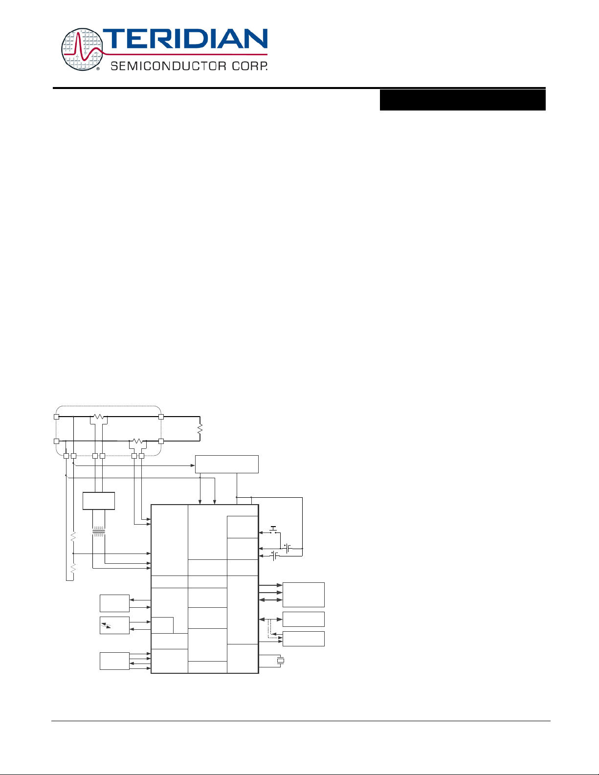
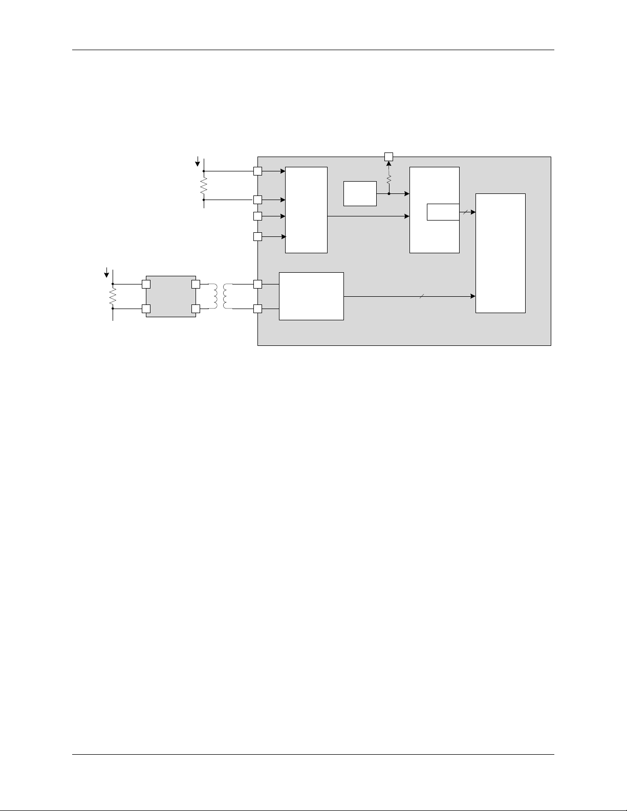
Figure 1: IC Functional Block Diagram
Page 10

1 Introduction
This data sheet covers the 71M6541D (32KB) , 71M6541F (64KB) and 71M6542F (64KB) fourth
generation Teri dian energy measurement S oCs. The t erm “71M 654x ” is used when discus si ng a dev ice
feature or behavior that is applicable to all three part numbers. The appropriate part num ber is i ndic ated
when a device feature or behav ior is being discussed that appl ies only to a specific part number. This
data sheet also cover s basic details about the companion 71M6x01 isolated c ur r ent sensor device. For
more complete information on the 71M6x01 sensors, r efer to the 71M6xxx Data Sheet.
This document covers the use of the 71M654x with local ly connected sensors as well when it is used in
conjunction wit h the 71M6x01 isolated current sensor. T he 71M 654x and 71M6x01 chipset make it
possible to use one non-isol ated and one isolated shunt cur r ent sensor t o c r eate single-phase and twophase energy meters using i nexpensive shunt resistors , while achieving unprecedented performance with
this type of sensor technology . The 71M654x SoCs also support confi gur ations involving one loc ally
connected shunt and one locally connected Curr ent Transformer ( CT), or two CTs.
To facilitat e doc um ent navigation, hyperlink s are often used to reference figures, tables and section
headings that are l oc at ed in other par ts of the document. All hyperlinks i n this document are highlight ed in
blue. Hyperlinks are used extensively to inc r ease the level of detail and clarity pr ov ided within each
section by refer enci ng other relevant parts of the document. To further facilitate document navigation, t his
document is published as a PDF docum ent with bookmarks enabled.
The reader is also encouraged to obt ain and review the documents listed in 8 Related Information on
page 162 of this document.
10 © 2008–2011 Teridian Semiconductor Corporati on v1.1
Page 11

2 Hardware Description
2.1 Hardware Overview
The Teridian 71M6541D/F and 71M6542F single-chip energy meter ICs integrate all primary functional
blocks required to implement a solid-state residential electricity meter. Included on the chip are:
• An analog front end (AFE) feat uri ng a 22-bit second-order sigma-delta ADC
• An independent 32-bi t digital computation engi ne ( CE) to implement DSP functions
• An 8051-compatible microprocessor (MPU) whic h ex ecutes one i nstr uc tion per clock cycle (80515)
• A precision voltage reference (VREF)
• A temperature sensor for digital temperature c om pensation:
- Metrology digital temperature compensation (MPU)
- Automatic RTC digital temper ature compensation operational in all power states
• LCD drivers
• RAM and Flash memory
• A real time clock (RTC)
• A variety of I/O pins
• A power failure interr upt
• A zero-crossing interrupt
• Selectable cur r ent sensor interfaces for loc ally -c onnec ted sensors as well as isolated sensors (i .e.,
using the 71M6x01 companion IC with a shunt resistor sensor)
• Resistive Shunt and Cur r ent Transformers are supported
Resistive Shunts and Current Transformers (CT) current sensors are supported. Resistive shunt curr ent
sensors may be connected directly to the 71M654x device or i sol ated using a companion 71M6x01
isolator IC in order to implement a variety of single-phase / split-phase (71M6541D/F) or two-phase
(71M6542F) metering configurations. An inexpensive, small size pulse transformer is used to isolate the
71M6x01 isolated sensor from the 71M654x. The 71M654x performs digital communications bidirectionally with the 71M6x01 and also provi des power t o the 71M6x01 through the isolating pulse
transformer. Isolated (remote) shunt current sensors ar e c onnec ted to the differenti al input of the
71M6x01. Included on t he 71M6x01 companion isolat or chip are:
• Digital isol ation communications interface
• An analog front end (AFE)
• A precision voltage reference (VREF)
• A temperature sensor (for digital temperature compensation)
• A fully diff er ential shunt resistor sensor input
• A pre-amplifier to optimize shunt current sensor perform anc e
• Isolated power circ uitry obtains dc power fr om pul ses sent by the 71M654x
In a typical application, the 32-bit compute engine (CE) of the 71M654x sequentially processes the samples
from the voltage inputs on analog input pins and from the external 71M6x01 isolated sensors and pe r forms
calculations to measure ac tive energy (Wh) and reactive energy (VA Rh) , as well as A
quadrant metering. These measurements are then ac cessed by the M P U, processed further and output
using the peripheral dev ices available to the MPU.
In addition to ad vanced measurement func t ions , the c loc k func tion allows the 71M6541D/F and 71M6542F
to record time-of-use (TOU) metering information for multi-rate applications and to time-stamp tamper or
other events. Measurements can be displayed on 3.3 V LCDs commonly used in low-temperature
environments. An on-chip charge pum p is available to drive 5 V LCDs. Flexible mapping of LCD display
segments facilitate integration of existing custom LCDs. Design trade-off bet ween the number of LCD
segments and DIO pins can be im plem ented in software to accommodat e various requi r ements.
2
h, and V2h for four-
In addition to the temperature-trimmed ultra-precisi on vol tage reference, the on-chip digital temperatur e
compensation mechanism includes a temperature sensor and associated controls for correction of unwanted
temperature effects on measurement and RTC accuracy, e.g., to meet the requirements of ANSI and IEC
standards. Temperature-dependent ext ernal components such as crystal oscillator, resistive sh unts, current
v1.1 © 2008–2011 Teridian Semiconductor Cor por ation 11
Page 12
∆Σ ADC
CONVERTER
VREF
MUX
VREF
VREF
VADC
22
FIR
IBP
IAP
VADC10 (VA)
IAN
IBN
71M6541D/F
CE RAM
*IN = Optional Neutral Current
Local
Shunt
IN*
CT
I
LINE
or
CT
11/5/2010
I
LINE
transformer s (CT s) and their corresponding signal conditioning ci rcuit s can be char ac terized and their
correcti on factors can be programmed to produce electricity meters with exc eptional accuracy over the
industrial t e mper ature ran ge.
One of the two internal UARTs is adapted to support an Infrared L ED with internal drive and s ens e con figuration
and can als o function as a stan dard UART. The optical output can be modulated at 38 kHz. This flexibility
makes it possible t o im plem ent AM R meter s with an IR int erface. A block diagram of the IC is shown in
Figure 1.
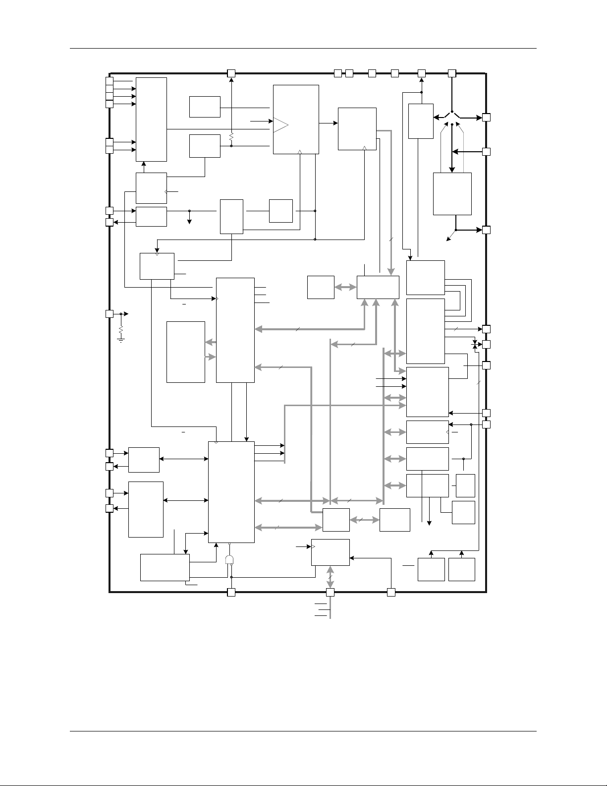
2.2 Analog Front End (AFE)
The AFE functions as a data acquisition system, controlled by the MPU. When used with locally
connected sensors, as seen i n Figure 2, the analog input signal s (IAP-IAN, VA and IBP-IBN) are
multiplexed to the ADC input and sampled by the ADC. The ADC output is decimated by the FIR filter
and stored in CE RAM where it can be accessed and proces sed by t he CE .
See Figure 6 for the m ultiplexer sequence correspondi ng to Figure 2. See Figure 35 for the meter
configurati on c or r espondi ng to Figure 2.
Figure 2. 71M6541D/F AFE Block Diagram (Local Sensors)
12 © 2008–2011 Teridian Semiconductor Corporati on v1.1
Page 13
∆Σ ADC
CONVERTER
VREF
MUX
VREF
VREF
VADC
22
FIR
IBP
IAP
VADC10 (VA)
IAN
IBN
71M6541D/F
CE RAM
71M6x01
SP
SN
INP
INN
Remote
Shunt
IN*
Digital
Isolation
Interface
Local
Shunt
I
LINE
22
11/5/2010
* IN = Optional Neutral Current
∆Σ ADC
CONVERTER
VREF
MUX
VREF
VREF
VADC
22
FIR
IBP
IAP
VADC10 (VA)
IAN
IBN
71M6542F
CE RAM
Local
Shunt
IB
CT
IA
or
CT
11/5/2010
IA
VADC9 (VB)
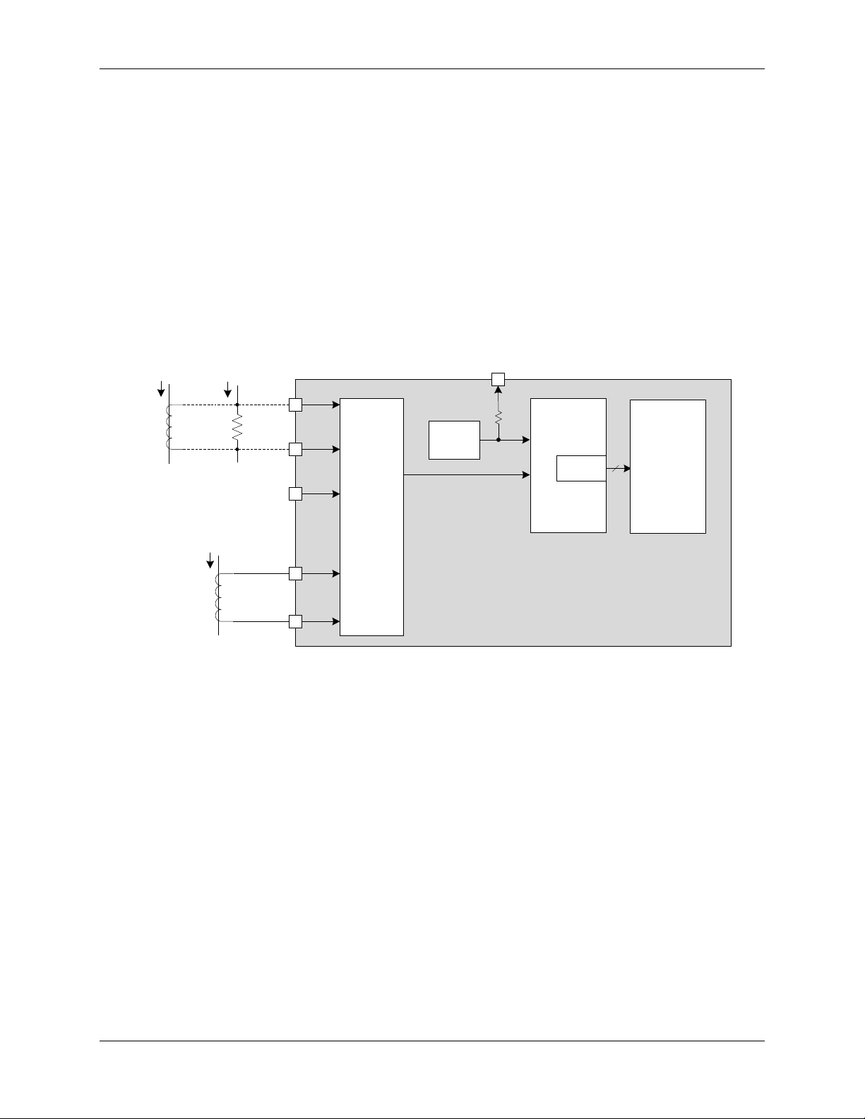
Figure 3 shows the 71M6541D/F multiplexer interface with one local and one remote resistive shunt
sensor. As seen in Figure 3, when a remote isolated shunt sensor is connected via the 71M6x01, the
samples associated with this current channel are not routed to the multipl ex er, and ar e instead
transferred digitally to the 71M6541D/F via the digital isol ation interface and are dir ectly stored in CE
RAM.
See Figure 6 for the m ultiplexer timing sequence correspondi ng to Figure 3. See Figure 36 for the meter
configurati ons corr espondi ng to Figure 3.
Figure 3. 71M6541D/F AFE Block Diagram with 71M6x01
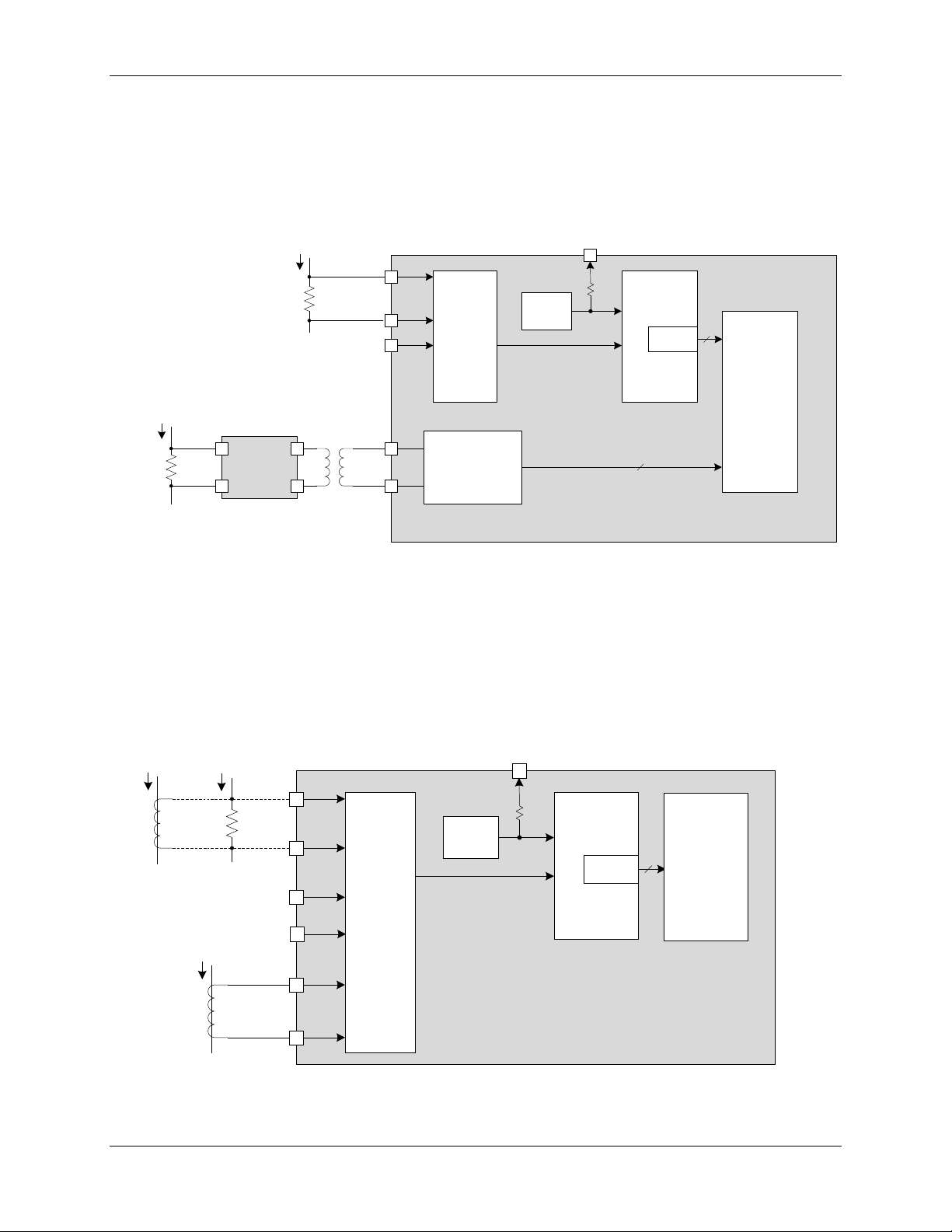
Figure 4 shows the 71M6542F AFE with locally connected sensors. The anal og input signals (IAP-IAN,
VA, IBP-IBN and VB) are multiplexed t o the ADC input and sampl ed by the ADC. The ADC out put is
decimated by the FIR filt er and stor ed in CE RAM where it can be accessed and processed by the CE.
See Figure 7 for the multiplexer timing sequence corresponding to Figure 4. See Figure 37 for the meter
configurati on c or r espondi ng to Figure 4.
v1.1 © 2008–2011 Teridian Semiconductor Cor por ation 13
Figure 4. 71M6542F AFE Block Diagram (Local Sensors)
Page 14
∆Σ ADC
CONVERTER
VREF
MUX
VREF
VREF
VADC
22
FIR
IBP
VADC9 (VB)
IAP
VADC10 (VA)
IAN
IBN
71M6542F
CE RAM
71M6x01
SP
SN
INP
INN
Remote
Shunt
IB
Digital
Isolation
Interface
Local
Shunt
IA
22
11/5/2010
Figure 5 shows t he 71M6542F multiplexer interface with one l oc al and one r em ote resistive shunt sensor.
As seen in Figure 5, when a remote isolat ed shunt sen sor is connected via the 71M6x01, the samples
associated with t his curr ent channel are not routed to the multi plex er , and are instead transferred digitally
to the 71M6542F via the digit al isolation interface and are di r ectly stored in CE RAM.
See Figure 6 for the multiplexer timing sequence corresponding to Figure 5. See Figure 38 for the meter
configurati ons corr espondi ng to Figure 5.
Figure 5. 71M6542F AFE Block Diagram with 71M6x01
2.2.1 Signal Input Pins
The 71M6541D/F f eatures five ADC inputs. The 71M6542F feat ur es six A DC input s.
IAP-IAN and IBP-IBN are intended for use as current sensor inputs. These four current sensor inputs can be
configured as four s ingle-ended inputs, or can be paired to form two differential inputs. For best
performance , it is reco m men ded to con figure the cu rrent sensor inputs as diffe ren tial inputs (i.e., IAP-IAN
and IBP-IBN). The first differential input (IAP-IAN) features a pre-amplif ier with a selectable gain of 1 or 8,
and is intended for dire c t conne ction to a shunt res istor sensor , and can also be us ed with a Cur ren t
Transformer (CT). The remaining differential pair (i.e., IBP-IBN) may be used with CTs, or may be enabled
to interface to a r emote 71M6x01 isolated current senso r providing isol ation for a sh unt resist or sensor using
a low cost pulse transformer.
The remaining input in the 71M6541D/F (VA) is single-ended, and is intended for sensing the line voltage in
a single-phase meter application using Equation 0 or 1 (see 2.3.4 Meter Equati ons on page 25). The
71M6542F features an additional single-ended voltage s ens ing input (VB) to su pport bi-phase applicat ions
using Equation 2. These s ingle-ended inputs are referenced to the V3 P3A pin.
All analog si gnal input pins measure voltage. In th e c ase of sh unt cur rent sensors, currents are sensed as a
voltage drop in the shunt resistor sens or . Referring to Figure 3, shunt sensors can be conne c ted dire c t ly to
the 71M654x (re ferre d to as a ‘loc al’ shunt sensor) or connec te d via an isolated 71M6x01 (referred to as a
‘remote’ shunt sensor). In the case of Cur ren t Transformers (CT), the current is measur ed as a voltage
across a bur den resistor that is connected to the secondary winding of the CT. Meanwhile, line voltages are
sensed through resistive voltage dividers. The VA and VB pins (VB is available in the 71M6542F only) are
single-ended and their c ommon return is the V3P3A pin.
Pins IAP-IAN can be programmed individually to be differential or single-ended as determined by the
DIFFA_E (I/O RAM 0x210C[4]) control bit. However, for most appli c ations, IAP-IAN are c onfigured as a
differential input to work wit h a shunt or CT directly interfaced to the IAP-IAN differential input with the
appropriate external signal conditioning components (see 4.2 Direct Connec tion of Sensors on page 92).
The performance of t he IAP-IAN pins can be enhanced by enabling a pr e-amplifier with a fixed gain of 8,
using the I/O RAM contr ol bit PRE_E (I/O RAM 0x2704[5]). When PRE_E = 1, IAP-IAN become the inputs
to the 8x pre-amplifi er, and the output of this amplifier is supplied to the multiplexer. The 8x amplification
14 © 2008–2011 Teridian Semiconductor Corporati on v1.1
Page 15

71M6542F
(hex)
Eq. 0 or 1
Eq. 2
FIR_LEN[1:0]
210C[2:1] 1 1
2
ADC_DIV
2200[5] 1 1
0
PLL_FAST
2200[4] 1 1
1
MUX_DIV[3:0]
2100[7:4] 3 3
4
MUX0_SEL[3:0]
2105[3:0] 0 0
0
MUX1_SEL[3:0]
2105[7:4] A A
A
MUX2_SEL[3:0]
2104[3:0] 2 2
2
MUX3_SEL[3:0]
2104[7:4] 1 1
9
RMT_E
2709[3] 0 0
0
DIFFA_E
210C[4] 1 1 1 DIFFB_E
210C[5] 1 1
1
EQU[2:0]
2106[7:5]
0 or 1
0 or 1
2
CE Code
--
CE41A01
CE41A01
CE41A04
Equations
--
0 or 1
0 or 1
2
--
1 Shunt and 1 CT
2 CTs
1 Shunt and 1 CT
2 CTs
1 Shunt and 1 CT
2 CTs
Applicable Figure
--
Figure 2
Figure 4
Figure 4
during initialization.
is useful when current sensor s with low sensitivit y, such as shunt r esi stor s, ar e used. With PRE_E set, the
IAP-IAN input signal am plitude is restricted t o 31.25 mV peak.
For the 71M 654x application utilizing two shunt resistor s ens o rs (Figure 3), the IAP-IAN pins are configured
for differential mode to interface to a local shunt by setting the DIFFA_E control bit. Meanwhile , the IBP-IBN
pins are re-configured as digital balanced pair to communicate with a Teridian 71M6x01 Isolated Sensor
interface by setting t he RMT_E control bit (I/O RAM 0x2709[3]). The 71M6x01 communicates with the
71M654x using a bi-directional digital data stream through an isolating low -cost pulse transformer. The
71M654x also supplies power to the 71 M6 x01 through the isola ting transformer. This type of interface is
further described at the end of this chapter (see 2.2.8 71M6x01 Isolated Sensor Interface (Remote Sensor
Interface)).
For use with Current Transformers (CTs), as shown in Figure 2, the RMT_E control bit is reset, so that the
IBP-IBN pins are c onfigured as local analog inputs. The IAP-IAN pins cannot be configured as a remote
sensor interf ac e.
2.2.2 Input Mu lt ip le x e r
When operating with local sensors, the input multiplexer sequentially applies the input signals from the analog
input pins to the input of the ADC (see Figure 2 and Figure 4). One complete sampling sequence is called a
multiplexer frame. The multiplexer of the 71M6541D/F can selec t up to three input signals (IAP-IAN, VA, and
IBP-IBN) per multiplexer frame as controlled by the I/O RAM control field MUX_DIV[3:0] (I/O RAM
0x2100[7:4]) (see Figure 6). T he multiplex er of t he 71M65 42F add s the VB signal to achiev e a total of
four inputs (see Figure 7). T he mult iplex er al way s sta rts at state 1 an d pro ceed s unt i l as many s tat e s
as determined by MUX_DIV[3:0] have been conv er ted.
The 71M65 41D/ F an d 71M 65 42F ea ch re qui r e a uni que CE c ode that is written f or the spec ific
appli c ation. M oreover, each CE code r equire s specific AFE and MUX settings in or der to function
properly. Table 1 prov ides the CE code and settings corresponding to the local sensor c onfigurations
shown in Figure 2 and Figure 4. Table 2 pr ov ides the CE code and sett ings corresponding to the
local/remote sensor configuration utilizing the 71M6x01 as shown in Figure 3 and Figure 5.
Table 1. Required CE Code and Settings for Lo cal Senso rs
I/O RAM
Mnemonic
Current Sensor Types
Notes:
TERIDIAN updates the CE code periodically. Please contact your local TERIDIAN representative to obtain the latest
CE code and the associated settings. The configuration presented in this table is set by the MPU demonstration code
I/O RAM
Location
71M6541D/E
(hex)
or
or
or
Table 2. Required CE Code and Settings for 71M6x01 isol at ed Sensor
v1.1 © 2008–2011 Teridian Semiconductor Cor por ation 15
Page 16

I/O RAM
Mnemonic
I/O RAM
Location
71M6541D/E
(hex)
71M6542F
(hex)
FIR_LEN[1:0]
210C[2:1] 1 1
ADC_DIV
2200[5] 1 1
PLL_FAST
2200[4] 1 1
MUX_DIV[3:0]
2100[7:4] 3 3
MUX0_SEL[3:0]
2105[3:0] 0 0
MUX1_SEL[3:0]
2105[7:4] A A
MUX2_SEL[3:0]1
2104[3:0] 1 9
MUX3_SEL[3:0]1
2104[7:4] 1 1
RMT_E
2709[3] 1 1
DIFFA_E
210C[4] 1 1
DIFFB_E
210C[5] 0 0
EQU[2:0]
2106[7:5]
0 or 1
0, 1 or 2
CE41B0162012
CE41B0166013
Equations
--
0, 1
0, 1 and 2
1 Local Shunt
1 Remote Shunt
1 Local Shunt
1 Remote Shunt
Applicable Figure
--
Figure 3
Figure 5
is set by th e MPU d em ons trati on c od e dur i ng in it i al iz ation.
CE Code --
Current Sensor Type --
Notes:
1. Although not used, set to 1 (the sample data is ignored by the CE)
2. 71M654x with 71M6201 remote sensor (200 Amps)
3. 71M654x with 71M6601 remote sensor (60 Amps)
TERIDIAN updates the CE code periodically. Please contact your local TERIDIAN representative
to obtain the latest CE code and the associated settings. The configuration presented in this table
and
and
Using settings for the I/ O RAM Mnemoni cs listed in Table 1 and Table 2 that do not match
those required by the corresponding CE co de being u sed results in unde sira bl e si de ef f ect s
and must not b e selected by the MPU. Consult your lo c al TERIDIAN repre se ntati ve to obtain
the correct CE co de and AFE / MU X s et t i ng s correspo nding to the application.
For a basic single-phase application, the IAP-IAN current input is configured for differential mode,
whereas the VA pin is single-ended and is typically connected to the phase voltage via a resistor divider.
The IBP-IBN differential input may be optionally used to s ens e the Neutral current. This configuration
implies that t he m ultiplexer applies a total of three inputs to the ADC. For this confi gur ation, the
multiplexer sequence is as shown in Figure 6. In this configuration IAP-IAN, IBP-IBN and VA are
sampled, the ext r a conversi on time slot (i.e., slot 2) is the optional Neutral curr ent, and the physical
current sensor for the Neutral current measurement m ay be omit ted if not required.
For a standard single-phase appl ication with tamper sensor in the neutral path, two current inputs can be
configured for differential mode, using the pin pair s IAP-IAN and IBP-IBN. This means that the multiplexer
applies a total of three inputs to the ADC. In this application, the system design may use two locally
connected current sensors via IAP-IAN and IBP-IBN, as show n in Figure 2, and configured as differential
inputs. Alternately, the IAP-IAN pin pair is con fig ure d as a diffe ren tial input and connected to a local current
shunt, and IBP-IBN is configured to connect to an isolated 71M6x01 isolated sensor (i.e., RMT_E = 1), as
shown in Figure 3. The VA pin is typically connected to the phase voltage via resistor div iders. For this
configuration, the multiplexer frame is also as sho wn in Figure 6 and time slot 2 is unused and ignored by
the CE, as the samples correspondi ng to the remote sensor (IBP-IBN) do not pass through the
multiplexer and are stored directly in CE RAM. The remote current sensor channel is sampled during t he
second half of the multiplexer frame and its timing rel ationship to the VA voltage is precisel y k nown so
that delay compensation can be properly applied.
The 71M6542F adds the ability to sample a second phase voltage (applied at the VB pin), which makes it
suitable for met er s with two voltage and two current sensors, such as m eters implementing Equation 2 for
dual-phase operation (P = VA*IA+VB*IB). Figure 7 shows the multiplexer sequence when four input s are
processed with l oc ally c onnec ted sensors, as shown in Figure 3. When using one loc al and one r em ote
senso r (Figure 5), the multiplexer sequence is also as shown in Figure 7.
16 © 2008–2011 Teridian Semiconductor Corporati on v1.1
Page 17
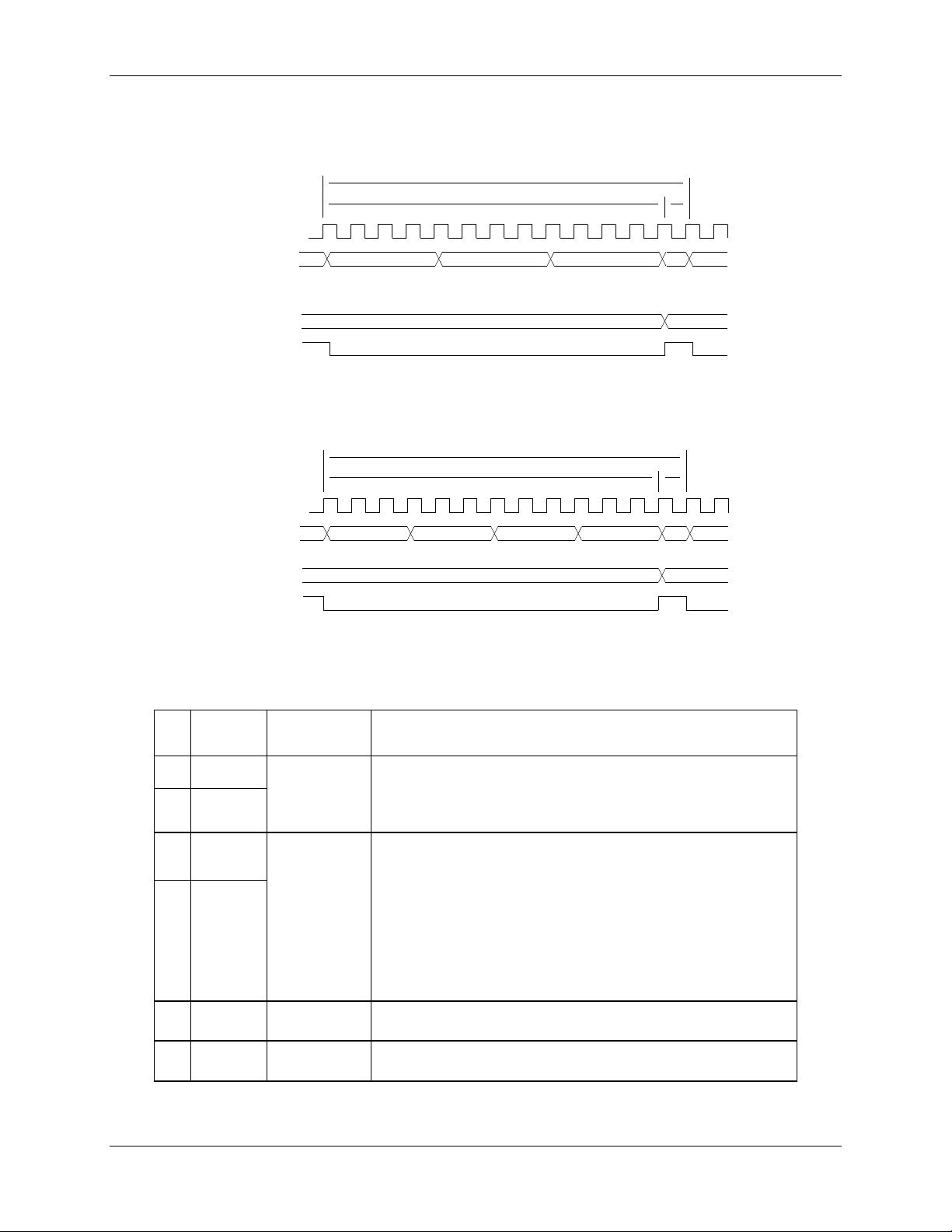
CK32
MUX STATE
00 1 2
MUX_DIV[3:0] = 3 Conversions
Settle
Multiplexer Frame
S
CROSS
MUX_SYNC
0S
11/5/2010
Fig. 2: IA VA IB
Fig. 3: IA VA Not Used
Fig. 5: IA VA VB
CK32
MUX STATE
0 1 2 3
MUX_DIV = 4 Conversions
Settle
Multiplexer Frame
S
CROSS
MUX_SYNC
0S
11/5/2010
Fig. 4: IA VA IB VB
disturbed.
For both multiplex er sequences sho wn in Figure 6 and Figure 7, the frame dur ation is 13 CK32 cycles
(where CK32 = 32768 Hz), t her ef or e, the resulting sample rate is 32768 Hz / 13 = 2520.6 Hz.
Table 3 summarizes the various AFE input configurations.
Figure 6: States in a Multipl exer Frame (MUX_DIV[3:0] = 3)
Figure 7: States in a Multipl exer Frame (MUX_DIV[3:0] = 4)
Table 3: ADC Input Configuration
Pin
ADC
Channel
IAP ADC0
IAN ADC1
Required
Setting
DIFFA_E = 1
Comment
Differential mode must be selected with DIFFA_E = 1 (I/O
RAM 0x21 0C[4]). The ADC results are stored i n CE RAM
location ADC0 (CE RAM 0x0), and ADC1 (CE RAM 0x1) is not
For locally connected sensors (Figure 2 and Figure 4), the
IBP ADC2
differential input must be enabled by setting DIFFB_E (I/O
RAM 0x21 0C[5].
IBN ADC3
DIFFB_E = 1
or
RMT_E = 1
For the r emote connected sensor (Figure 3 and Figure 5)
with a remote shunt sensor, RMT_E (I/O RAM 0x2709[3])
must be set.
In both cases , the ADC results are stored in RA M loca tion
ADC2 (CE R AM 0x2 ), and ADC3 (CE RAM 0x3 ) is not
disturbed.
VA ADC10 --
VB ADC9 --
Multiplexer adv anc e, FIR initiation and chopping of the ADC reference voltage (using the internal CROSS
signal, see 2.2.7 Voltage References) are cont r olled by the internal MUX_CTRL circuit. Additionally,
v1.1 © 2008–2011 Teridian Semiconductor Cor por ation 17
Single-ended mode only . The ADC resul t is stored in RAM
location ADC10 (CE RAM 0xA).
Single-ended mode only ( 71M 6542F only). The ADC result
is stored in RAM location ADC9 (CE RAM 0x9).
Page 18

MUX_CTRL launches each pass of the CE through its code. Conceptually, MUX_CTRL is clocked by
CK32, the 32768 Hz clock from the PLL block. The behavior of the MUX_CTRL circuit is governed by:
• CHOP_E[1:0] (I/O RAM 0x2106[3:2])
• MUX_DIV[3:0] (I/O RAM 0x2100[7:4])
• FIR_LEN[1:0] (I/O RAM 0x210C[2:1])
• ADC_DIV (I/O RAM 0x2200[5])
The duration of each multiplexer state depends on the number of ADC sampl es processed by the FI R as
determined by the FIR_LEN[1:0] (I/O RAM 0x210C[2:1] control field. Each multiplexer state starts on the
rising edge of CK32, t he 32-kHz clock.
It is recomm ended that MUX_DIV[3:0] (I/O RAM 0x220 0[ 2:0]) be s et to zero whi le cha nging the ADC
confi guration. Although not required, it minimizes system transients that might be caused by momentary
shorts between the AD C inpu ts, especially when changing the DIFFn_E control bits (I/O RAM 0x210C[5:4]).
After the configuration bits are set, MUX_DIV[3:0] should be set to the required value.
Additionall y , t he ADC can be configured to operate at ½ rate (32768*75=2.46MHz). In this mode, the
bias current to the ADC am plifiers is reduced and overall system power i s reduced. The ADC_DIV (I/O
RAM 0x2200[5]) bit selects full speed or half speed. At half speed, if FIR_LEN[1:0] is set to 01 (288),
each conversion requir es 4 XTAL cy cl es, r esul ting in a 2520Hz sample rate when MUX_DIV[3:0] = 3.
Note that in order to work with these power-reduci ng se ttings, a corresponding CE c ode is required.
The duration of each time sl ot in CK32 cycles depends on FIR_LEN[1:0], ADC_DIV and PLL_FAST:
Time_Slot _Dur ation (PLL_FAST = 1) = (FIR_LEN[1:0]+1) * (ADC_DIV+1)
Time_Slot _Dur ation (PLL_FAST = 0) = 3*(FIR_LEN[1:0]+1) * (ADC_DIV+1)
The duration of a multiplexer frame in CK32 cycles is:
MUX_Frame_Durati on = 3-2*PLL_FAST + Time_Slot_Duration * MUX_DIV[3:0]
The duration of a multiplexer frame in CK_FIR c ycle s is:
MUX frame duration (CK_FI R c ycles) =
[3-2*PLL_FAST + Time_Slot_Dur ation * MUX_DIV] * (48+PLL_FAST*102)
The ADC conversion sequence is progr ammable through the MUXx_SEL control fields (I/O RAM 0x2100
to 0x2105). As stated above, there are three ADC time slots in the 71M6541D/F and four ADC time slots
in the 71M6542F, as set by MUX_DIV[3:0] (I/O RAM 0x2100[7:4]). In the expression MUXx_SEL[3:0] = n, ‘x’
refers to the multiplexer frame time slot number and n refers to the desired ADC input number or ADC handle
(i.e., ADC0 to ADC10, or simply 0 to 10 decimal). Thus, there are a total of 11 valid ADC handles in the
71M654x devices. For example, if MUX0_SEL[3:0] = 0, then ADC0, corresponding to the sample from the
IAP-IAN input (configured as a differential input), is positioned in the multiplexer frame during time slot 0. See
Table 1 and Table 2 f or the appropriate MUXx_SEL[3:0] settings and other settings applic able to a
particular CE code.
Note that whe n the remote s ensor interface is enabled, and even though th e samples corresponding to
the remote sensor current (IBP-IBN) do not pass t hrough the mul tiplexer, the MUX2_SEL[3:0] and
MUX3_SEL[3:0] control fields must be written wit h a v alid ADC handle that is not being used. Typically,
ADC1 is used for this purp ose (see Table 2). I n this manne r , the ADC1 handle, whic h is not used i n the
71M6541D/F or 71M65 42F, i s used a s a place holder in the multiplex er fram e, in order to gener ate th e
correct multiplexer frame sequence and the correct s ampl e r ate. The re sul ti n g sampl e dat a st or ed in
CE RAM 0x1 is undefined and is ignored by the CE code. Meanwhile, the digital isol ation interface t akes
care of automatically storin g the sample s for the remote interfac e current (IBP-IBN) in CE RAM 0x2.
Delay compensati on and other functions in the CE code require the settings for MUX_DIV[3:0],
MUXx_SEL[3:0], RMT_E, FIR_LEN[1:0], ADC_DIV and PLL_FAST to be fixed for a given CE code.
Refer to Table 1 and Table 2 for the settings that are applicable to the 71M6541D/F and
71M6542F.
18 © 2008–2011 Teridian Semiconductor Corporati on v1.1
Page 19

MUX5_SEL[3:0]
MUX6_SEL[3:0]
2102[3:0]
Selects the ADC input conver ted during time slot 6.
2102[7:0]
Selects the ADC input conver ted during time slot 7.
MUX9_SEL[3:0]
Controls the rat e of the ADC and FIR cl oc k s.
MUX_DIV[3:0]
PLL_FAST
Determines the num ber of ADC cycles i n the ADC decimation FIR filter.
DIFFA_E
210C[5]
Enables the diff er ential configuration for analog input pins IBP-IBN.
PRE_E
o
delay
o
delay
ft
T
t
360360 ⋅⋅=⋅=
φ
Table 4 summarizes t he I/ O RAM registers used for configuring the multiplexer, signals pins, and ADC.
All listed registe rs are 0 after reset a nd wake from battery m odes, and are readable and wri table.
Table 4: Multiplexer and ADC Configuratio n Bi t s
Name Location Description
MUX0_SEL[3:0]
MUX1_SEL[3:0]
MUX2_SEL[3:0]
MUX3_SEL[3:0]
MUX4_SEL[3:0]
2105[3:0] Selects the ADC input converted during time slot 0.
2105[7:4] Selects the ADC input converted during time slot 1.
2104[3:0] Selects the ADC input converted during time slot 2.
2104[7:4] Selects the ADC input converted during time slot 3.
2103[3:0] Selects the ADC input converted during time slot 4.
2103[7:4] Selects the ADC input converted during time slot 5.
MUX7_SEL[3:0]
MUX8_SEL[3:0]
2101[3:0] Selects the ADC input converted during time slot 8.
2101[7:0] Selects the ADC input converted during time slot 9.
MUX10_SEL[3:0]
ADC_DIV
2100[3:0] Selects the ADC input converted during time slot 10.
2200[5]
2100[7:4] The number of ADC time slots in each multiplexer frame (maximum = 11).
2200[4] Contr ols the speed of the PLL and MCK.
FIR_LEN[1:0]
210C[1]
210C[4] Enables the differential confi gur ation for analog input pins IAP-IAN.
DIFFB_E
Enables the remote sensor interface transforming pins IBP-IBN into a
RMT_E
2709[3]
digital bal anc ed differential pair f or communications with the 71M6x01
sensor.
2704[5] Enables the 8x pre-amplifier.
Refer to Table 76 start ing on page 111 for more complete details about these I/O RAM locations.
2.2.3 Delay Compensation
When measuring the energy of a phase (i .e., Wh and VARh) in a service, the volt age and current for that
phase must be sampled at the same instant . Otherwise, the phase difference, Ф, introduces errors.
Where f is the frequency of t he input signal, T = 1/f and t
voltage.
Traditionally, sampling is accomplished by using two A/D converters per phase (one for voltage and the
other one for curr ent) c ontrolled to sample simultaneously . Teridian’s Single-Converter Technology
however, exploits the 32-bit signal processing capabi lity of its CE to implement “constant delay” all-pass
filters. The all-pass filter corrects for the conver si on time diff er enc e between the voltage and the
corresponding current samples that are obtai ned with a single multiplexed A/D converter.
The “constant del ay ” all -pass fi lter provides a broad-band delay 360
the difference in sample time between the voltage and the current of a given phase. This digital filter
does not affect the amplit ude of the signal, but provides a preci sel y cont r olled phase response.
The recommended ADC multiplexer sequence samples the cur r ent fi r st, immediately foll owed by
sampling of the corr espondi ng phase voltage, thus the voltage is delayed by a phase angle Ф relative to
the current. The delay compensation implemented in the CE aligns the voltage sam ples with their
corresponding current samples by first delaying the current samples by one full sample interval (i.e.,
o
), then routing the voltage samples through t he all-pass filter, thus delaying the voltage samples by
360
v1.1 © 2008–2011 Teridian Semiconductor Cor por ation 19
is the sampling delay between current and
delay
o
– θ, which is precisely matched t o
®
,
Page 20

360o - θ, resulting in the residual phase error between the cur r ent and its corresponding v oltage of θ – Ф.
The residual phase error is negligible, and is typi c ally less than ±1. 5 mil li-degrees at 100Hz, thus it does
not contribute to errors in the energy measurements.
When using remote sensors, t he CE performs the same delay compensati on described above to align
each voltage sam ple with its corresponding current sam ple. Ev en though the remote current sam ples do
not pass through the 71M654x multiplexer, their timing relationship to their corresponding voltages is
fixed and precisel y known, provided that the MUXn_SEL[3:0] slot assignment fields are programmed as
shown in Table 1 and Table 2.
2.2.4 ADC Pre-Amplifier
The ADC pre-amplifier is a low-noise differential amplifier with a fix ed gain of 8 available only on the IAPIAN sensor input pins. A gain of 8 is enabled by setting PRE_E = 1 (I/O RAM 0x2704[5]). When disabled,
the supply current of t he pr e-am plifier is <10 nA and the gain is unity. With proper settings of the PRE_E
and DIFFA_E (I/O RAM 0x210C[4]) bits, the pre-ampl if ier can be u sed wh et he r dif ferential mode is
selected or not. F or best performance, the differ ential mode is recommended. In order to save power, the
bias current of the pre -amplifier and AD C is adjusted acco rdi ng to the ADC_DIV control bit (I/O RAM
0x2200[5]).
2.2.5 A/D Converter (ADC)
A single 2nd order delta-sigma A/D converter digitizes the voltage and current inputs to the device. The
resolution of the ADC, including the sign bit, is 21 bits (FIR_LEN[1:0] = 1, I/O RAM 0x210C[2:1]) , or 22 bits
(FIR_LEN[1:0] = 2). The ADC is clocked by CKA DC.
Initiation of each ADC conversion is contro lled by MUX_CTRL internal circuit as described above. At the
end of each ADC conversion, the FIR filter output data is stored into the CE RAM location determined by
the multiplexer selection. FIR data is stored LSB justified, but shifted left 9 bits.
2.2.6 FIR Fi lter
The finite impulse response filter is an integral part of the ADC and it is optimized for use with the multiplexer.
The purpose of the FIR filter is to decimate the ADC output to the desired resol ution. At the end of each
ADC conversion, t he output data is stored into the fixed CE RAM location det ermined by the multiplexer
selection as shown in Table 1 and Table 2.
2.2.7 Voltage References
A bandgap circuit provides the reference voltage to the ADC. The amplifier within the reference is chopper
stabilized, i.e., the chopper ci r c uit can be enabled or disabled by the MPU using the I/O RAM control field
CHOP_E[1:0] (I/O RAM 0x2106[3:2]). The two bits in the CHOP_E[1:0] field enable the MPU to operate the
chopper circuit in regular or inverted oper ation, or in toggling m odes (recommended). When the
chopper circuit is toggled in betwe en multiplexer cycl es, dc off sets on VREF are automatically be
averaged out, ther efore the chopper circuit shoul d always be conf igured for one of the toggli ng m odes.
Since the VREF band-ga p a mp lifie r is chopper-stabilized, the dc offset volt age, which is the most
significant long-term drift mechanism in the voltage references (VREF ) , is automatically remov ed by the
chopper circ uit. B oth the 71M654x and the 71M6x01 feature chopper circuit s for their respective VREF
voltage ref er enc e.
The general topology of a chopped am plifier is shown in Figure 8. The CROSS signal is an int er nal onchip signal and is not accessibl e on any pin or register.
20 © 2008–2011 Teridian Semiconductor Corporati on v1.1
Page 21
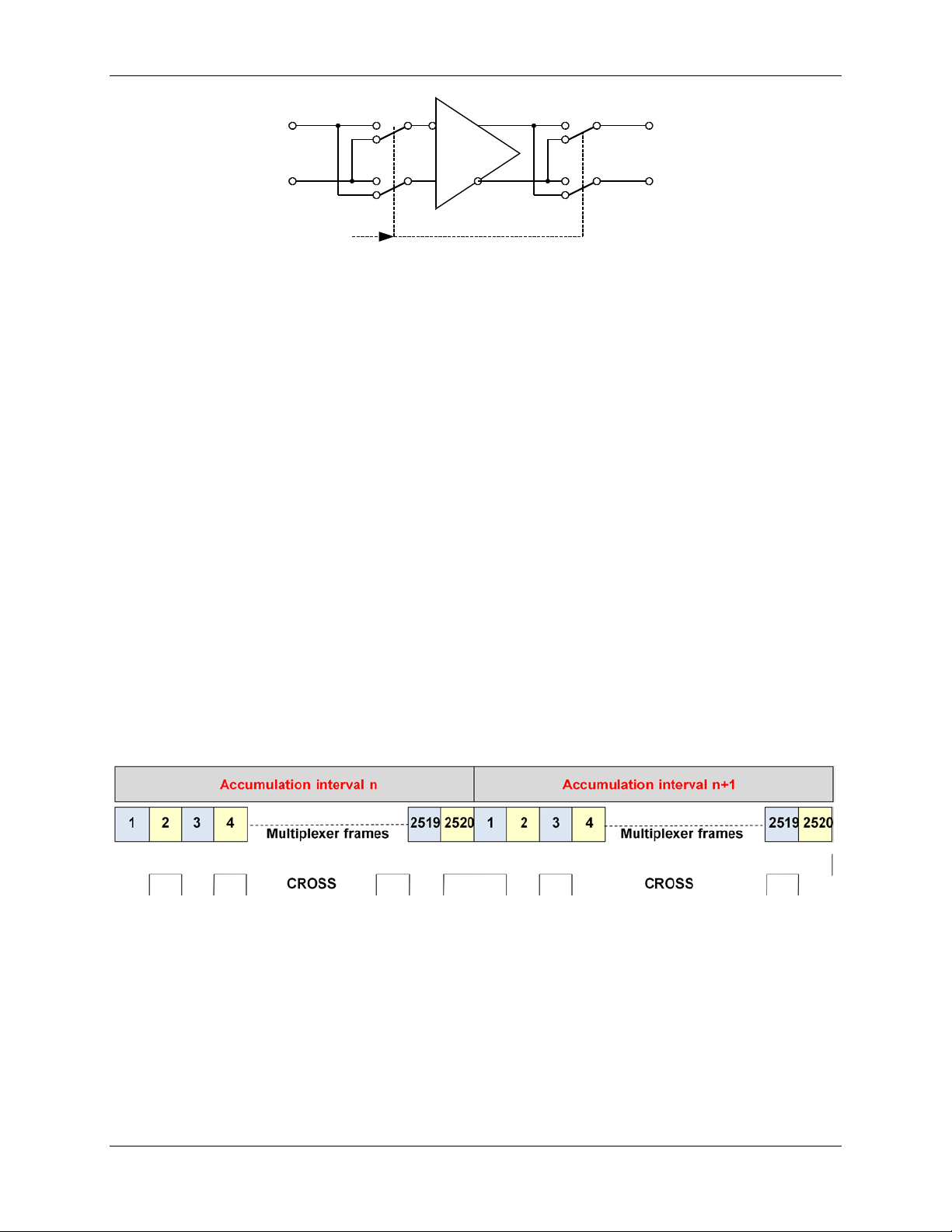
G
-
+V
inp
V
outp
V
outn
V
inn
CROSS
A
B
A
B
A
B
A
B
Figure 8: General Topology of a Chopped Amplifier
It is as s umed that an offset v oltage Voff appears at the positive amplifi er input. With all switches, as
controlled by CROSS (an internal si gnal) , in the A position, the output voltage is:
Voutp – Voutn = G (Vinp + Voff – Vinn) = G (Vinp – Vinn) + G Voff
With all switches set to the B position by applying the inverted CROSS signal, the output volt age is:
Voutn – Voutp = G (Vinn – Vinp + V off ) = G (Vinn – Vinp) + G Voff, or
Voutp – Voutn = G (Vinp – Vinn) - G Voff
Thus, when CROSS is toggl ed, e.g., after each multiplex er cycl e, the offset alternatel y appears on the
output as positiv e and negative, which results in the offset effectively bei ng elimi nated, regardless of its
polarity or magnitude.
When CROSS is high, the connection o f the a mp lifie r input devices is reversed. This preserves the overall
polarity of that amplifier gain; it inverts its inpu t o ffse t. By alternately reversing the connection, the amplifier’s
offset is averaged t o z er o. This rem ov es the most signif icant long-term drift m echani sm in the voltage
reference. The CHOP_E[1:0] (I/O RAM 0x2106[3:2]) control field controls the beh avio r of CROSS. The
CROSS signal reverses the amplifier connection in the voltage reference in orde r to negate the effects o f its
offset. On the first CK32 rising edge after the last multiplexer state of its sequence, the multi plex er wait s
one additional CK 32 cycle before beginning a new frame. At the beginning of this cycle, the value of
CROSS is updated according to the CHOP_E[1:0] field. The extra CK32 cycle allows time for the
chopped VRE F to settle. During this cycle, MUXSYNC is held high. The leading edge of MUXSYNC initiates
a pass through the CE program sequence. The beginning of the sequence is the serial readout of the four
RTM words.
CHOP_E[1:0] has four states: positive, reverse, and two toggle stat es. In t he posi tive state, CHOP_E[1:0]
= 01, CROSS is held low. In the reverse state, CHOP_E[1:0] = 10, CROSS is held high.
Figure 9: CROSS Signal with CHOP_E = 00
Figure 9 shows CROSS over two accumulation intervals when CHOP_E[1:0] = 00: At the end of the
first interval, CROSS is high, at the end of the second interval, CROSS i s low. Op er a tion wit h
CHOP_E[1:0] = 00 does not require control of the chopping mechanism by the MPU.
In the second toggle state, CHOP_E[1:0] = 11, CROSS does not toggle at the end of the last multiplexer
cycle in an accumul ation interval.
A second, low-power volt age r eference is used in the LCD system and for the comparators that support
transiti ons to and from the bat tery modes.
v1.1 © 2008–2011 Teridian Semiconductor Cor por ation 21
Page 22

Command
Phase Selecto r
Associated TMUXRn
Control Field
000
Invalid
00
Invalid
---
001
Command 1
01
TMUXRB [2:0]
100
Reserved
101
Invalid
110
Reserved
2.2.8 71M6x01 Isolated Sensor Interface (Remote Sensor Interface)
2.2.8.1 General Description
Non-isolati ng sensors, such as shunt r esi stors, can be connected to the inputs of the 71M654x via a
combination of a pulse tr ansformer and a 71M6x01 IC (a top-level block diagr am of t his sensor i nterface
is shown in Figure 36). The 71M6x01 receives power directly from the 71M654x via a pulse transformer
and does not require a dedicated power supply circuit. The 71M6x01 establishes 2-way communication
with the 71M654x, suppl yi ng c ur r ent samples and auxiliary information such as sensor temperatur e v ia a
serial data stream .
One 71M6x01 Isolated Se nsor c an be su pported by the 71M6541D/F and 71M6 542F . When remote
interface IBP-IBN is enabled, the two analog current inputs pins IBP and IBN become a digital balanced
differential interface to the remote sensor. See Table 3 for details.
Each 71M6x01 Isol ated Sensor consists of the following building blocks:
• Power supply for power pulses received from the 71M654x
• Digital communications interface
• Shunt signal pre-amplifier
• Delta-Sigma ADC Conv erter with precision bandgap reference (chopping amplifi er )
• Temperature sensor
• Fuse system contai ning par t-specific informati on
During an ordinar y multiplexer cycle, the 71M654x internally determines which other channels are
enabled with MUX_DIV[3:0] (I/O RAM 0x2100[7:4]). At the same time, it decimates the modulator output
from the 71M6x01 Isolated Sensors. Eac h r esul t is written to CE RAM duri ng one of its CE acc ess time
slots. See Table 3 for the CE RAM locations of the sampled signals.
2.2.8.2 Communication between 71M654x and 71M6x01 Isolated Sensor
The ADC of the 71M6x01 derives its timing from the power pulses generated by the 71M654x and as a
result, o perates its ADC slaved to the frequency of the power pulses. The generation of power pulses, as
well as the communication protocol between the 71M654x and 71M6x01 Isolated Sensor is automatic and
transparent to the user. Details are not covered in this data sheet.
2.2.8.3 Control of the 71M6x01 Isolated Sensor
The 71M654x can read or write certain types of information from each 71M6x01 isolated sensor.
The data to be read is selected by a combination of the RCMD[4:0] and TMUXRn[2:0]. To perform a read
transaction from one of the 71M6x01 devices, the MPU first writes the TMUXRn[2:0] field (where n = 2, 4, 6,
located at I/O RAM 0x270A[2:0], 0x270A[6:4] and 0x2709[2:0], respectively). Next, the MPU writes
RCMD[4:0] (SFR 0xFC[4:0]) with the desi r ed c ommand and phase select ion. When the RCMD[4:2] bits
have cleare d to zero, the trans ac tion has been complete d and the requested data is av ailabl e in
RMT_RD[15:0] (I/O RAM 0x260 2[ 7:0] is the MSB and 0x2603[7:0] is the LSB). The read parity error bit,
PERR_RD (SFR 0xFC[6]) is also updated during the transaction. If the MPU writes to RCMD[4:0] before a
previously init iated read transacti on is completed, the command is ignored. Therefore, the MPU must wait
for RCMD[4:2]=0 before proceeding to issue the next remote sensor read command.
The RCMD[4:0] field is divided into two sub-fields, COMMAND=RCMD[4:2] and PHASE=RCMD[1:0], as
shown in Table 5.
Table 5. RCMD[4:0] Bits
RCMD[4:2]
RCMD[1:0]
22 © 2008–2011 Teridian Semiconductor Corporati on v1.1
IBP-IBN
Page 23
111
Reserved
Notes:
is invalid and must not be used.
TRIMT[7:0]
Notes:
The CHOP settings for the isolated sensors.
11 – Same as 00
1. Only two codes of RCMD[4:2] (SFR 0xFC[4:2]) are relevant for normal
operation. These are RCMD[4:2] = 001 and 010. Codes 000 and 101
are invalid and will be ignor ed if used. The remaining codes are
reserved and must not be used.
2. For the RCMD[1:0] control field, codes 01, 10 and 11 are valid and 00
Table 6 shows the allowable combinations of val ues i n RCMD[4:2] and TMUXRn[2:0], and the
corresponding data ty pe and format sent back by the 71M6x01 isolated sensor and how the data is stored
in RMT_RD[15:8] and RMT_RD[7:0]. The MPU selects which of the three phase s i s read by asserting the
proper code in the RCMD[1:0] field, as shown in Table 5.
Table 6: Remote Interface Read Commands
RCMD[4:2] TMUXRn[2:0] Read Operation RMT_RD [15:8] RMT_RD [7:0]
001 00X
010 00X
010 01X
010 10X
1. TRIMT[7:0] is the VREF trim value for all 71M6x01 devices. Note that the TRIMT[7:0] 8-bit v alue i s for med
by RMT_RD[8] and RMT_RD[7:1]. See the 71M6 xxx Data shee t f or more information on TRIMT[7:0]
2. See the 71M6xxx Data Sheet for the equation to calculate temperature from the
the 71M 6x 01.
3. See the 71M6xxx Data Sheet for the equation to calculate temperature from the
the 71M 6x 01.
(trim fuse for all 71M6x01)
STEMP[10:0]
(sensed 71M6x01 temperature)
VSENSE[7:0]
(sensed 71M6x01 supply v oltage)
VERSION[7:0]
(chip version)
TRIMT[7]=RMT_RD[8] TRIMT[6:0]=RMT_RD[7:1]
STEMP[10:8]=RMT_RD[10:8]
(RMT_RD[15:11] are sign ext en ded )
All zeros VSENSE[7:0]
VERSION[7:0] All zeros
STEMP[7:0]
STEMP[7:0] value read from
VSENSE[7:0] value read from
With hardware and trim-related information on each c onnected 71M6x01 Isolated Sensor available to the
71M6541D/F, the MPU can implement temperature compensation of the energy measurement based on the
individual t em per ature characteristic s of the 71M6x01 Isolated Sensor. See 4.7 M etrology Temperature
Compensation on page 97 for details.
Table 7 shows all I/O RAM registers used for c ontrol of the external 71M6x01 Isol ated Sensors. See the
71M6xxx Data Sheet for addi tional details.
Table 7: I/O RAM Control Bits for Isolated Sensor
Name Address
RST
Default
WAKE
Default
R/W Description
When the MPU wr ites a non-zero value to RCMD,
the 71M654x issues a command to the cor-
RCMD[4:0]
SFR
FC[4:0]
0 0 R/W
responding isol ated sensor selected with
RCMD[1:0]. When the command is complete, the
71M654x clears RCMD[4:2]. The command code
itself is in RCMD[4:2].
The 71M654x sets these bits to i ndicate that a
PERR_RD
PERR_WR
SFR FC[6]
SFR FC[5]
0 0 R/W
parity error on the i sol ated sensor has been detected. Once set, the bits are remember ed until
they are cleared by the MPU.
CHOPR[1:0]
v1.1 © 2008–2011 Teridian Semiconductor Cor por ation 23
2709[7:6] 00 00 R/W
00 – Auto chop. Change every multiplexer frame.
01 – Positive
10 – Negative
Page 24

Default
Default
TMUXRB[2:0]
270A[2:0]
000
000
R/W
The TMUX bits for control of the isolated sensor.
RMT_RD[15:8]
2602[7:0]
Refer to Table 76 start ing on page 111 for more complete details about these I/O RAM locations.
Name Address
RMT_RD[7:0]
RFLY_DIS
RMTB_E
RST
2603[7:0]
210C[3]
2709[3] 0 0 R/W
0 0 R The read buffer for 71M6x01 read operations.
0 0 R/W
WAKE
R/W Description
Controls how the 71M654x drives the 71M6x01
power pulse. When set, the power pulse i s driven
high and low. When cleared, it is driven high
followed by an open circ uit flyback interval.
Enables the isolated remote sensor interface and
re-configures pins IBP-IBN as a balanced pair
digital remote interface.
2.3 Digital Computation Engine (CE)
The CE , a dedicated 32-bit signal pro cess or, per forms the preci sion computati ons necessary to ac curately
measure energy. The CE cal c ulations and processes include:
• Multiplicati on of each current sample with its associated voltage sample to obtain the energy per
sample (when multi plied with the constant sample time).
• Frequency-insensitive delay cancellation on all four channels (to compensate for the delay between
samples caused by the multiplexing scheme).
• 90° phase shifter (for VAR calc ulations).
• Pulse generation.
• Monitoring of the input signal frequency (for frequenc y and phase i nformation).
• Monitoring of the input signal amplitude (for sag detec tion).
• Scaling of the processed sam ples based on calibration coefficients.
• Scaling of sampl es based on temperature compensation information.
2.3.1 CE Program Memory
The CE program resides in flash memory. Common access to flash memory by the CE and MPU is controlled
by a memory share circuit. Each CE instr uc tion word is two bytes long. Allocated flash space for the CE
program cannot exceed 4096 16-bi t words (8 KB). The CE program counter begins a pass through the
CE code each time multi plex er state 0 begins. The code pass ends when a HALT instruction is executed.
For proper operation, the code pass must be completed before the multiplexer cycle ends.
The CE program must begin on a 1 KB boundary of the flash addre ss. The I/O RAM con trol field
CE_LCTN[5:0] (I/O RAM 0x2109[5:0]) def i nes whic h 1 KB boundary contains the CE code. Thus, the first
CE instruction i s l oc ated at 1024*CE_LCTN[5:0].
2.3.2 CE Data Memory
The CE and MPU share data memory (RAM). Common access to XRA M by the CE and MP U is con tro lled
by a memory share circuit. The CE can access up to 3 KB of the 3 KB data RAM (XRAM), i.e., from RAM
address 0x0000 to 0x0C00.
The XRAM can be accessed by the FIR filter block, the RTM circuit, the CE, and the MPU. Assigned time
slots are reserved for FIR and MPU, respectively, to prevent bus contention for XRAM data access by the CE.
The MPU reads and writ es the XRAM shared between the CE and MPU as the primary m eans of data
communicati on between the two processors.
Table 3 shows the CE addresses in XRAM al located to analog input s from the AFE.
The CE is aided by support hardware to facilitate implementation of equations, pulse counters, and
accumulators. This hardware is controll ed through the I/O RAM contro l field EQU[2:0], equation assist
(I/O RAM 0x2106[7:5]), bit DIO_PV (I/O RAM 0x2457[6]), bit DIO_PW, pulse count assist (I/O RAM
0x2457[7]), and SUM_SAMPS[12:0], accumulation assist (I/O RAM 0x2107[4:0] and 0x2108[7:0]).
24 © 2008–2011 Teridian Semiconductor Corporati on v1.1
Page 25
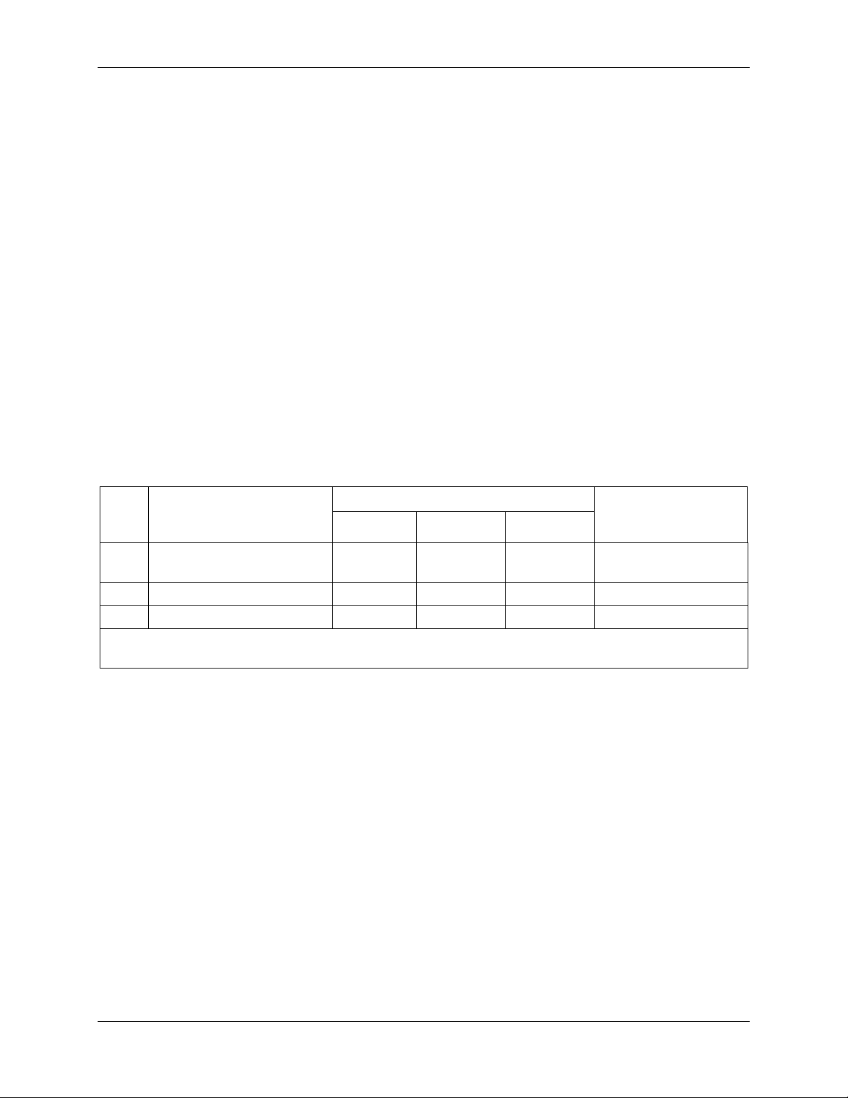
1. Optionally , I B may be used to m easure neut r al c ur r ent
SUM_SAMPS[12:0] supports an accumulation scheme where the incremental energy values from up to
SUM_SAMPS[12:0] multiplexer frames are added up over one accumulation interval. The integr ation time
for each energy output is, for example, SUM_SAMPS[12:0]/2520.6 (with MUX_DIV[3:0] = 011, I/O RAM
0x2100[7:4] and FIR_LEN[1:0] = 10, I/O RAM 0x210C[2:1]). CE hardware issues the XFER_BUSY interrupt
when the accumulation is complete.
2.3.3 CE Communication with the MPU
The CE outputs six signals to the MPU: CE_BUSY, XFER_BUSY , XPULSE, YPULSE, WPULSE and
VPULSE. These are connected to the MPU interrupt servic e. CE_B USY indicates that the CE is actively
processing data. This signal occurs once every multiplexer frame. XFER_BUSY indicates that the CE is
updating to the ou t put region of the CE RAM, whic h oc c urs whenever an accumulation cycle has been
completed. Both, CE_BUSY and XFER_BUSY are cleared when the CE executes a HALT instruction.
XPULSE, YPULSE, VPULSE and WPULSE can be configured to interrupt the MP U and indic ate sag
failures, zero crossings of the mains voltage, or other significant ev ents. Additionally, these signals can
be connected direc tly to DIO pins to provide direct outputs f or the CE. Interrupt s associated with these
signals always occur on t he leading edge (see “External” interrupt source No. 2 in Figure 16).
2.3.4 Meter Equations
The 71M6541D/F and 71M6542 F provide hardware as s istance to the CE in order to support var ious meter
equations. This assistance is controlled through I/O RAM register EQU[2:0] (equation assist). The Compute
Engine (CE) firmwa re fo r industrial configurat ions can im ple men t the equations listed in Table 8. EQU[2:0]
specifies the equat ion to be used based on the meter configurati on and on the number of phases used for
metering.
Table 8: Inputs Selected in Multiplexer Cycles
Wh and VARh formula Recommended
EQU
1-element, 2-W, 1φ with
0
neutral curr ent sense
1
1-element, 3-W, 1φ
2 †
Note:
† 71M6542F only
2-elem ent, 3-W, 3φ Delta
Description
Element 0 Element 1 Element 2
VA ∙ IA VA ∙ IB1 N/A IA VA IB1
VA(IA-IB)/2 N/A N/A IA VA IB
VA ∙ IA VB ∙ IB N/A I A VA IB VB
Multiplexer
Sequence
2.3.5 Real-Time Monit or (RTM)
The CE contains a Real-Time Monitor (RTM), which can be programm ed to monitor four selectable
XRAM locations at full sample rate. The four monitored locati ons, as select ed by the I/O RAM registers
RTM0[9:8], RTM0[ 7:0], RTM1[9:8], RTM1[7:0] , RTM2[ 9:8], RTM2[7:0], RTM3[9:8] , and RTM3[7:0], are
serially output to the TMUXOUT pin via the digital output multiplexer at the beginning of each CE code
pass. T he RTM c an be enabled and disabl ed with c o nt rol bit RTM_E (I/ O RAM 0x 2106[1] ). T he RTM
output is clocked by CKTEST. Each RTM word is clocked out in 35 CKCE cycles (1 CKCE cycle is
equivalent to 203 ns) and cont ains a leading flag bit. See Figure 10 for the RTM output format. RTM is
low when not in use.
Figure 11 summariz es the timing relationships between the input MUX states, the CE_BUSY signal, and
the RTM serial output str eam . In this example, MUX_DIV[3:0] = 4 (I/O RAM 0x2100[7:4]) and
FIR_LEN[1:0] = 10 ( I/O RAM 0x210C [1]), (384), resulting in 4 ADC conversi ons. A n ADC conver si on
always consumes an integer num ber of CK32 cl oc k s. Followed by the conversions is a single CK 32
cycle.
Figure 11 also shows that the RTM serial data stream begins transmitting at the beginning of state S.
RTM, consisting of 140 CK cycl es, always f inishes before the next CE c ode pass starts.
v1.1 © 2008–2011 Teridian Semiconductor Cor por ation 25
Page 26
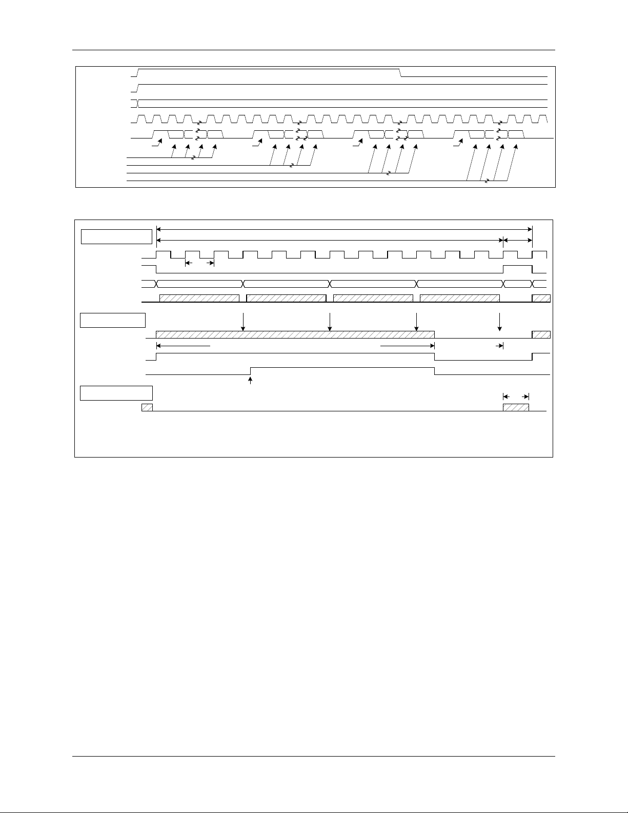
CK32
MUX STATE
0
MUX_DIV Conversions, MUX_DIV=4 is shown
Settle
ADC MUX Frame
ADC EXECUTION
S
MUX_SYNC
S
CE_EXECUTION
RTM
140
MAX CK COUNT
0 450
150
900 1350 1800
ADC0 ADC1 ADC2 ADC3
CK COUNT = CE_CYCLES + 1CK for e ach ADC transfer
NOTES:
1. ALL DIMENSIONS ARE 5 MHZ CK COUNTS.
2. THE PRECISE FREQUENCY OF CK IS 150*CRYSTAL FREQUENCY = 4.9152MHz.
3. XFER_BUSY OCCURS ONCE EVERY SUM_SAMPS CODE PASSES.
CE_BUSY
XFER_BUSY
INITIATED BY A CE OPCODE AT END OF SUM INTERVAL
ADC TIMING
CE TIMING
RTM TIMING
1 2 3
CKTEST
RTM
FLAG
RTM DATA0 (32 bits)
LSB
SIGN
LSB
SIGN
RTM DATA1 (32 bits)
LSB
LSB
SIGN
SIGN
RTM DATA2 (32 bits)
RTM DATA3 (32 bits)
0 1 30 31 0 1 30 31
0 1
30 31 0 1 30 31
FLAG FLAG FLAG
MUX_STATE S
MUX_SYNC
CK32
Figure 10: R TM Timing
Figure 11: Timing relationship between ADC MUX, CE, and RTM Serial Transfer
26 © 2008–2011 Teridian Semiconductor Corporati on v1.1
Page 27

2.3.6 Pulse Generators
The 71M6541D/F and 71M6542F provide four pulse generators, VPULSE, WPULSE, XPULSE and YPULSE,
as well as hardware support for the VPULSE and WPULSE pulse generator s. The pulse generators can
be used to output CE status indic ators, SAG for example, to DIO pins. All pul ses can be configured to
generate inter r upts to the MPU.
The polarity of the pulses may be inverted with control bit PLS_INV (I/O RAM 0x2 10C[0]). When this bit is
set, the pulses are active high, rather than the more usual active low. PLS_INV i nverts all the pulse output s.
The function of each pulse generator is determined by the CE code and t he MPU code m ust c onfigure the
corresponding pulse outputs in agreement with the CE code. For example, s tandard CE code produces a
mains zero-crossing pulse on XPULSE and a SAG pulse on YPULSE.
A common use of the zero-crossing pulses is to generate interrupt in order to drive real-time clock software
in places where the mai ns fr equenc y is sufficiently accurate to do so and also to adjust for crystal aging.
A common use for the SAG pulse is to generate an interrupt that alerts the MPU when mains power is about
to fail, so that the MPU code can stor e ac c um ulated energy and other data to EEPROM before t he
V3P3SYS supply voltage actually dr ops.
2.3.6.1 XPULSE and YPULSE
Pulses generated by the CE may be ex ported to the XPULSE and YPULSE pulse output pins. Pin s
SEGDIO6 and SEGDIO7 are used for these pulses, respectively. Generally, the XPULSE and YPULSE
outputs can be updated once o n each pa s s of the CE code.
See 5.3 CE Interface Description on page 125 for detail s.
2.3.6.2 VPULSE and WP U LSE
Referring to Figure 12, duri ng each CE code pa s s the hardware stores export ed WPULSE and VPULSE sign
bits in an 8-bit FIFO and outputs them at a specified interval. This permits the CE code to calculate the
VPULSE and WPULSE outputs at the beginning of its code pass and to rely on hardware to spread them
over the multiplexer frame. As seen in Figure 12, the FIFO is reset at the beginning of each m ultiplexer
frame. As also seen in Figure 12, the I/O RAM register PLS_INTERVAL[7:0] (I/O RAM 0x210B[7:0])
controls the delay to th e first puls e update and t he interv al between subs equent updat es. The LSB of
the PLS_INTERVAL[7:0] register is equivalent to 4 CK_FIR cycles (CK_FIR is typically 4.9152MHz if
PLL_FAST=1 and ADC_DIV=0, but other CK_FIR frequencies are possible; see the ADC_DIV definition in
Table 76.) If PLS_INTERVAL[7:0]=0, the FIFO is deactivated and the pulse outputs are updated immediately.
The MUX frame duration in units of CK_FIR clock cycles is given by:
If PLL_FAST=1:
MUX frame dur ati on in C K_FI R c y cles = [1 + (FIR_LEN+1) * (ADC_DIV+1) * (MUX_DIV)] * [150 / (ADC_DIV+1)]
If PLL_FAST=0:
MUX frame dur ati on in C K_FI R c y cles = [3 + 3* (FIR_LEN+1) * (ADC_DIV+1) * (MUX_DIV)] * [48 / (ADC_DIV+1)]
PLS_INTERVAL[7:0] in units of CK_FI R clock cyc les i s calc ulated by:
PLS_INTERVAL[7:0] = floor (Mux frame duration in CK_F IR cyc les / CE pulse u pdat es per Mux frame / 4 )
Since the FIFO resets at t he beginning of each multiplexer frame, t he user must specify
PLS_INTERVAL[7:0] so that all of the possible pulse updates occurri ng in one CE execution are output
the multiplexer f rame complet es. For instance, the 71M654x CE code outputs six updates per
before
multiplexer int erval, and if the multiplexer interval is 1950 CK_FIR clock cycles long, the ideal value for
the interv al is 1950/6/4 = 81.25. However, if PLS_INTERVAL[7:0] = 82, the sixth out put occ urs too late and
would be lost. In this case, the proper value for PLS_INTERVAL[7:0] is 81 (i.e., round down the result).
Since one LSB of PLS_INTERVAL[7:0] is eq ual to 4 CK_FIR clock cycles, the p ulse t i me in terval TI in u nit s of
CK_FIR clock cycle s is:
T
= 4*PLS_INTERVAL[7:0]
I
v1.1 © 2008–2011 Teridian Semiconductor Cor por ation 27
Page 28
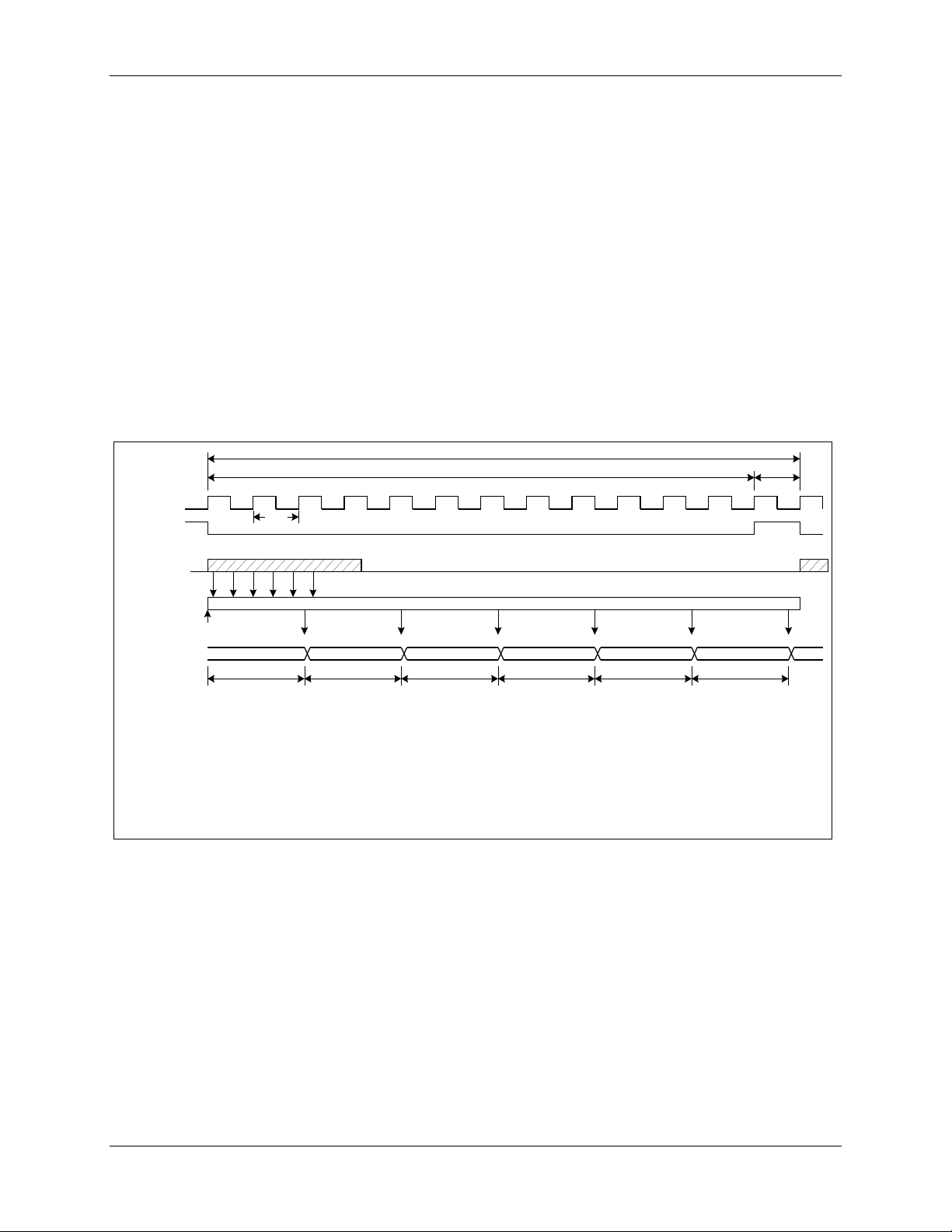
CK32
MUX_DIV Conversions (MUX_DIV=4 is shown)
Settle
ADC MUX Frame
MUX_SYNC
150
WPULSE
S0S
1
S
2S3
S
4
S
5
CE CODE
RST
W_FIFO
S
0
S
1
S
2
S
3
S
4
S
5
S
0
S
1
S
2
S
3
S
4
S
5
4*PLS_INTERVAL
2. If WPULSE is low longer than (2*PLS_MAXWIDTH+1) updates, WPULSE will be raised until the next
low-going pulse begins.
3. Only the WPULSE circuit is shown. The VARPULSE circuit behaves identically.
4. All dimensions are in CK_FIR cycles (4.92MHz).
5. If PLS_INTERVAL=0, FIFO does not perform delay.
4*PLS_INTERVAL
4*PLS_INTERVAL
4*PLS_INTERVAL
4*PLS_INTERVAL
4*PLS_INTERVAL
1. This example shows how the FIFO distributes 6 pulse generator updates over one MUX frame.
If the FIFO is enab led (i.e ., PLS_INTERVAL[7:0] ≠ 0), hardware also provides a maximum pulse width feature
in control register PLS_MAXWIDTH[7:0] (I/O RAM 0x210A) . By default, WPULSE and VPULSE are negative
pulses ( i. e . , low level pu lses, designed to s ink c ur r ent through an LED) . PLS_MAXWIDTH[7:0] determines the
maximum negative pul se wi dt h T
in uni t s of CK_FI R cl oc k cy cl es bas ed on t he p ul s e interv al TI
MAX
accordi ng to the form ula:
= (2 * PLS_MAXWIDTH[7:0] + 1) * TI
T
MAX
If PLS_MAXWIDTH = 255 or PLS_INTERVAL=0, no pulse width checking is perf ormed, and the pulses
default to 50% duty cycl e. T
is typicall y program m ed to 10 ms., which works well with most cali br ation
MAX
systems.
The polarity of the pulses may be inverted with the control bit PLS_INV (I/O RAM 0x210C[0]). When
PLS_INV is set, the pulses are active high. The default value for PLS_INV is zero, which selects active low
pulses.
The WPULSE and VPULSE pulse generator outputs are available on pins SEG DIO 0/W P ULSE and
SEGDIO1/VPULSE, respect ively (pins 45 and 44). The pulses can also be output on OPT_TX pin 53
(see OPT_TXE[1:0], I/O RAM 0x2456[3:2] for details).
Figure 12. Pu ls e Ge ne r a tor FIFO Timing
2.3.7 CE Functional Overview
The 71M654x provi des an ADC and multiplexer to sample the analog curr ent s and voltages as seen in
Figure 2 and Figure 3. The VA and VB voltage sensors ar e formed by resistive voltage dividers directly
connected to the 71M 654x dev ic e, and t her efore always use the ADC and multiplexer facilities in the
71M654x device. Cur r ent sensors, however, may be connected dir ec tly to the 71M654x or remotely
connected through an isolated 71M6x01 device. The remote 71M6x01 sensor has its own separate ADC
and voltage ref er enc e. W hen a current sensor is connected via a 71M6x01 isolated sensor, the 71M654x
places the sampl e data rec eiv ed digitally over the isolation interface (via t he pulse transformer) in the
appropriate CE RAM location, as shown in Figure 3. The ADCs (i.e., ADC in the 71M 654x and the ADC in
the 71M6x01) process their corresponding sensor channels providing one sample per channel per
multiplexer cycle.
Figure 14 (71M6541D/F) and Figure 15 (71M6542F) show the sampli ng sequence when both curr ent
sensors (IA and IB) are connected directly to the 71M 6541D/F as seen in Figure 2. However, when the IB
28 © 2008–2011 Teridian Semiconductor Corporati on v1.1
Page 29
XFER_BUSY
Interrupt to MPU
20ms
833ms
channel is a 71M6x01 isolated sensor, the sample data does not pass through the 71M6541D/F
multiplexer, as seen in Figure 3. In this case, the sample i s tak en duri ng the second half of the multipl ex er
cycle and the data is dir ectly stor ed in the corresponding CE RAM loc ation as indicated in Figure 3. The
timing relati onshi p between the remote current sensor c hannel and its corresponding voltage is precisely
defined so that delay c om pensation can be properly appli ed by the CE.
Referring to Figure 15, the 71M6542F feat ur es an additional voltage input (VB) permitting the
implementati on of a t wo-phase met er . As with VA, the VB voltage divider is directly connect ed to the
71M6542F and uses the ADC and multi plexer faciliti es in the 71M6542F. MUX_DIV[3:0] = 4 configures
the multiplex er to pr ov ide an additional time slot to accommodate the additional VB voltage sam ple. As
with the 71M6541D/F , IA sam ples are obt ained from a current sensor that i s di r ectly connected to the
71M6542F, while IB samples may be obtained from a directly connected CT or a remotely connected
shunt using a 71M6x01 isolated device as seen in Figure 2 and Figure 3.
The number of samp les pro ces s ed dur ing one ac cu mu lation cycle is con tro lled by the I/ O RAM register
SUM_SAMPS[12:0] (I/O RAM 0x2107[4:0], 0x2108[7:0]). The integration time for each energy output is:
SUM_SAMPS / 2520.6, where 2520.6 is the sample rate in Hz
For exam ple, SUM_SAMPS = 2100 establishes 2100 samples per accumul ation cycle, wh ich has a
duration of 833 ms. After an accum ulation cycle is completed, the XFER_B US Y i nterr upt signals to the
MPU that accumulated data are available.
The end of each multiplexer cycle is signaled to the MPU by the CE_BUSY interrupt. At the end of each
multiplexer cycle, status information, such as sag data and the digitized input signal, is available to the MPU.
Figure 13 shows the accum ulation interval r esul ting from SUM_SAMPS = 2100, consisti ng of 2100
samples of 397 µs each, followed by the XFER_BUSY interrupt. The sampling in this example is appli ed
to a 50 Hz signal. There is no correlation between the line signal frequenc y and the choice of
SUM_SAMPS. Furthermore, sampling does not have to start when the li ne v oltage crosses the zero line,
and the length of the accumulation interval need not be an integer multiple of the signal cycles.
Figure 13: Accumulation Interval
v1.1 © 2008–2011 Teridian Semiconductor Cor por ation 29
Page 30
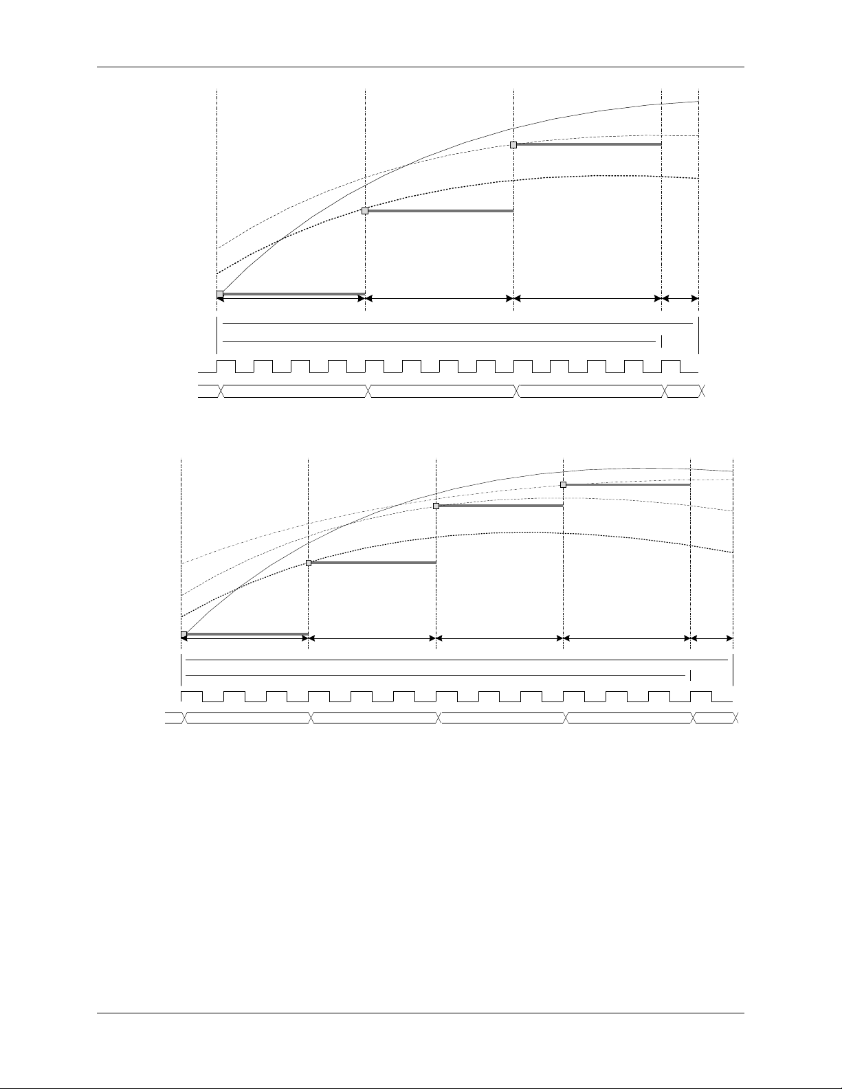
MUX STATE
CK32
(32768 Hz)
0 1 2
MUX_DIV[3:0] = 3 Conversions
Settle
Multiplexer Frame (13 x 30.518 µs = 396.7 µs -> 2520.6 Hz)
SS
IA
VA
IB
30.5
µs
122.07 µs
122.07 µs 122.07 µs
MUX STATE
CK32
(32768 Hz)
0 31 2
MUX_DIV[3:0] = 4 Conversions
Settle
Multiplexer Frame (13 x 30.518 µs = 396 µs à2520Hz)
S
S
IA
VA
IB
30.5 µs
91.5 µs
91.5 µs 91.5 µs
91.5 µs
VB
Figure 14: Samples from Multiplexer Cycle (MUX_DIV[3:0] = 3)
Figure 15: Samples from Multiplexer Cycle (MUX_DIV[3:0] = 4)
30 © 2008–2011 Teridian Semiconductor Corporati on v1.1
Page 31

000
4.9152 MHz
011
614.4 kHz
110
2.4 80515 MPU Core
The 71M6541D/F and 71M 6542F include an 80515 MPU (8-bit, 8051-compatible) that processes most
instructions in one clock cycle. Using a 4.9 MHz clock results in a processing throughput of 4.9 MIPS. The
80515 architecture eliminates redundant bus states and implements parallel execution of fetch and execution
phases. Normally, a machine cycle is aligned with a memory fetch, therefore, most of the 1-byte instructions
are p erf o rm e d i n a si ngl e machine cycle (MP U clock cycle). This leads to an 8x average performance
improvement (in terms of MIPS) over the Intel
Table 9 shows the CKMPU frequency as a func tion of the MCK clock (19.6608 MHz) divided by the MPU
clock divider which is set in the I/O RAM control field MPU_DIV[2:0] (I/O RAM 0x2200[2:0]). Actual processor
clocking speed can be adjusted to the total processing demand of t he application (metering calc ulations,
AMR management, memory management, LCD driver management and I/O management) using
MPU_DIV[2:0], as shown in Table 9.
Table 9: CKMPU Clock Frequencies
MPU_DIV [2:0]
001 2.4576 MHz
010 1.2288 MHz
100
101
8051 device running at the same cloc k fr equenc y.
CKMPU Frequency
307.2 kHz
111
Typical measurement and metering functions based on the r esul ts provided by the internal 32-bit compute
engine ( CE) are avail able for the MPU as part of the Teridian standard l ibr ary. T e ri dian pr ovi des
demonstration source code to help reduce the design cycle.
2.4.1 Memory Organization and Addressing
The 80515 MPU core incorporates the Harvard architecture with separate code and data spaces. Memory
organization in the 8051 5 is s imila r to th a t o f the industry standard 8051. There are three me mory areas:
Program memory (Flash, shared by MPU and CE), external RAM (Data RAM, shared by the CE and MPU,
Configuration or I/O RAM), and internal data memory (Internal RAM). Table 10 shows the memory map.
Program Memory
The 80515 can address up to 64 KB of program memory space (0x0000 to 0xFFFF). Program memory is
read when the MPU fetches instr uc tions or performs a MOVC operation.
After reset, the MPU starts program execution from program mem or y loc ation 0x0000. The lower part of
the pro gram memory i nc ludes reset and inte r rupt vect ors. The int errupt vectors are sp aced at 8-byte
intervals, starting from 0x0003.
MPU External Data Memory (XRAM)
Both internal and ext er nal m em or y is physically located on the 71M654x device. The external memory
referred in this documentation is only external to the 80515 MPU core.
3 KB of RAM starting at address 0x0000 i s shared by the CE and M P U. The CE normally uses the first
1 KB, leaving 2 KB for the MPU. Diff erent v er si ons of the CE c ode use varying amounts. Consult the
documentati on for the specific code version being used for the exact limit.
v1.1 © 2008–2011 Teridian Semiconductor Cor por ation 31
If t he M P U ov er wri tes the CE’s working RAM, the CE’s output may be corrupted. If the CE is
disabled, the first 0x40 bytes of RAM are still unusable while MUX_DIV[3:0] ≠ 0 because the
71M654x ADC writes to t hese l oc ations. Setting MUX_DIV[3:0] = 0 disables the ADC output
preventing t he CE fr om writi ng the fi r st 0x 40 by tes of RAM.
In addition, MUXn_SEL[3:0] v alues must be written only after writing MUX_DIV[3:0].
Page 32

(XRAM)
MPU
The 80515 writes into exter nal data memory when the MPU executes a MOVX @Ri,A or MOV X
@DPTR,A instructi on. The MPU reads external data memory by exec uting a MOVX A,@Ri or MOVX
A,@DPTR instruction (PDATA, SFR 0xBF, provides the upper 8 bytes for the MOVX A,@Ri instruction).
Internal and External Memory Map
Table 10 shows the address, t y pe, use and size of the various memory components.
Table 10: Memory Map
Address
(hex)
0000-7FFF F lash Memory Non-volatile
0000-0BFF Static RAM Volatile
2000-27FF Static RAM Volatile
2800-287F Static RAM
Memory
Technology
Memory
Type
Non-volatile
(battery)
Name T ypi cal Usag e
MPU Program and
Program memory
for MPU and CE
non-volatil e data
CE program (on 1
KB boundary)
External RAM
Configuration
RAM (I/O RAM)
Configuration
Shared by CE and
Hardware control 2 KB
Battery-buffered
RAM (I/O RA M)
memory
Memory Size
(bytes)
64/32 KB †
3 KB max.
5/3 KB †
128
0000-00FF Static RAM Volatile Internal RAM Part of 80515 Core 256
† Memory size depends on IC. See 2.5.1 Physical Memory for details.
MOVX Addressing
There are two types of instructions differing in whether they provide an 8-bit or 16-bit indirect addr ess to
the external data RA M.
In the first type, MOVX A,@Ri, the contents of R0 or R1 in the current register bank pr ov ide the eight
lower-ordered bits of addr es s. The eight high-ordered bits of the address are speci fied with the PDATA
SFR. This method allows the user paged acce ss (256 pages of 256 bytes each) to all ranges of the
external dat a RAM.
In the second type of MOVX instruc tion, MOVX A,@DPTR, the data pointer gener ates a 16-bit address.
This form is faster and m or e eff icient when accessing very l ar ge data arrays (up to 64 KB), since no
additional instr uc tions are needed to set up the eight high ordered bits of the address.
It is possible to mix the t wo MOVX types. Thi s provides the user with four separate dat a pointers, two
with direct access and two with paged ac c es s, to the entire external mem or y range.
Dual Data Pointer
The Dual Data Pointer ac c eler ates the block moves of data. The standard DPTR is a 16-bit register that
is used to address external m em or y or peripherals. In the 80515 core, the standard data pointer is called
DPTR, the second data poi nter is called DPTR1. The data pointer select bit, located in the LSB of the DPS
register (DPS[0], SFR 0x92), chooses the active pointer. DPTR i s selected when DPS[0] = 0 and DPTR1 is
selected when DPS[0] = 1.
The user switches between pointers by toggling the LSB of the DPS register. The values in the data pointers
are not affected by the LSB of the DPS regis ter. A ll DPTR related instructions us e th e cu rrently selected
DPTR for any activit y .
The second data point er may not be supported by c er tain compilers.
DPTR1 is useful for copy routines, where it can make the inner loop of the routine two instructions faster
compared to the reloading of DPTR from registers. Any interrupt routine using DPTR1 must save and
restore DPS, DPTR and DPTR1, which increases stack usage and slows down interrupt latency.
By selecting the R80515 core in the Keil compiler project settings and by using the compiler directive
“MODC2”, dual data pointers are enabled in certain library routines.
32 © 2008–2011 Teridian Semiconductor Corporati on v1.1
Page 33

E8
IFLAGS
EF
D0
PSW D7
B8
IEN1
IP1
S0RELH
S1RELH PDATA
BF
A0
P2
A7
90
DPS
97
88
TCON
TMOD
TL0
TL1
TH0
TH1
CKCON
8F
80
87
An alternative data pointer is available in the f orm of the PDATA register (SFR 0xBF), sometimes referr ed
to as USR2). It defi nes the high byte of a 16-bit address when reading or writing XDATA with the ins tru ction
MOVX A,@Ri or MOVX @Ri,A.
Internal Data Memory Map and Access
The Internal dat a memory pr ov ides 256 byt es (0x00 to 0xFF) of data memory. The internal data memory
address is always 1 byte wide. Table 11 shows the internal data mem ory map.
The Special Funct ion Registers (SFR) occup y the upper 128 bytes . The SFR area of internal data memory
is available only by di r ect addr essing
. Indirect addressing of this area accesses the upper 128 bytes of
Internal RAM. The lower 128 bytes contai n working registers and bit addr essable memory. The lower 32
bytes form four banks of eight registers (R0-R7). Two bits on the program memory st atus wo rd (PSW, S FR
0xD0 ) select which bank is in use. The next 16 bytes form a block of bit addressable memory space at
addresses 0x00-0x7F. All of the bytes in the lower 128 bytes are acc essible through direct or indir ec t
addressing.
Table 11: Internal Data Memory Map
Address Range Direct Addressing Indirect Addressing
0x80 0xFF Special Function Registers (SFRs) RAM
0x30 0x7F Byte addressable area
0x20 0x2F Bit addressable area
0x00 0x1F Register banks R0…R7
2.4.2 Special Function Registers (SFRs)
A map of the Special Function Registers is sh own in Table 12.
Only a few addresses in the SFR memory space are occupied, the others are not implemented. A read
access to unimplemented addresses returns undefined data, while a write access has no effect. SFRs
specific to the 71M654x are shown in bold print on a shaded field. The registers at 0x80, 0x88, 0x90,
etc., are bit addressable, all others are byte addressable.
Table 12: Special Function Regi st er Map
Hex/
Bin
F8
Addressable
X000 X001 X010 X011 X100 X101 X110 X111
INTBITS VSTAT
F0 B F7
E0 A E7
D8 WDCON DF
C8 T2CON CF
C0 IRCON C7
Bit
B0
P3 (DIO12:15)
FLSHCTL
A8 IEN0 IP0 S0RELL AF
(DIO8:11)
98 S0CON S0BUF IEN2 S1CON S1BUF S1RELL
P1(DIO4:7)
Byte Addressable
RCMD SPI_CMD
ERASE
FF
FLSHPG
EEDATA EECTRL
Bin/
Hex
B7
9F
P0 (DIO0:3) SP DPL DPH DPL1 DPH1 PCON
v1.1 © 2008–2011 Teridian Semiconductor Cor por ation 33
Page 34

P0
SP
0x82
0x00
Data Pointer Low 0
35
DPH
PCON
0x87
0x00
UART Speed Control
39
0x88
0x00
Timer/Count er Contr ol
42
TMOD
0x8A
0x00
Timer 0, low byte
39
TH0
CKCON
0x90
0xFF
Port 1
36
DPS
S0CON
0x99
0x00
Serial Port 0, Data Buffer
36
IEN2
S1RELL
0x9D
0x00
Serial Port 1, Reload Regi ster , low byte
36
0xA0
0xFF
Port 2
36
IEN0
P3
IP1
0xBA
0x03
Serial Port 0, Reload Regi ster , high byte
36
S1RELH
PDATA
High address byte f or MOVX@Ri - also called USR2
0xC0
0x00
Interrupt Request Contr ol Register
42
T2CON
0xF0
0x00
B Register
35
2.4.3 Generic 80515 Special Function Registers
Table 13 shows the location, description and reset or power-up value of the generic 80515 SFRs. Additio nal
descriptions of the registers can be found at the page numbers listed in the tabl e.
Table 13: Generic 80515 SFRs - Location and Reset Val ues
Name
DPL
DPL1
DPH1
TCON
TL0
TL1
TH1
P1
S0BUF
S1CON
S1BUF
Address
(Hex)
0x80 0xFF Port 0 36
0x81 0x07 Stack Poi nter 35
0x83 0x00 Data Pointer High 0 35
0x84 0x00 Data Pointer Low 1 35
0x85 0x00 Data Pointer High 1 35
0x89 0x00 Timer Mode Control 40
0x8B 0x00 Tim er 1, high byte 39
0x8C 0x00 Timer 0, low byte 39
0x8D 0x00 Timer 1, high byt e 39
0x8E 0x01 Cl oc k Contr ol ( Str etch=1) 36
0x92 0x00 Data Pointer sel ec t Register 32
0x98 0x00 Serial Port 0, Cont r ol Register 38
0x9A 0x00 Interrupt Enable Register 2 42
0x9B 0x00 Serial Port 1, Control Register 38
0x9C 0x00 Serial Port 1, Data Buffer 36
Reset value
(Hex)
Description Page
P2
0xA8 0x00 Interrupt Enable Register 0 41
IP0
S0RELL
IEN1
S0RELH
IRCON
PSW
WDCON
A
B
34 © 2008–2011 Teridian Semiconductor Corporati on v1.1
0xA9 0x00 Interrupt Priority Register 0 45
0xAA 0xD9 Serial Port 0, Reload Register, low byte 36
0xB0 0xFF Port 3 36
0xB8 0x00 Interrupt Enable Register 1 41
0xB9 0x00 Interrupt Priority Register 1 45
0xBB 0x03 Serial Port 1, Reload Register, high by te 36
0xBF 0x00
0xC8 0x00 Polarity for INT2 and I NT3 42
0xD0 0x00 Program Status Word 35
0xD8 0x00 Baud Rate Control Register (only WDCON[7] bit used) 36
0xE0 0x00 Accumulator 35
32
Page 35

P
Accumulator (ACC, A, SFR 0x E0):
ACC is the accumulator register. Most instru c tions use the accumulator to hold t he oper and. The
mnemonics for accumulator-specifi c instr uc tions refer to accumul ator as A, not ACC.
B Register (SFR 0xF0):
The B re gister is us ed duri ng multiply and divide i nstructions. It ca n also be used as a scratch-pad register
to hold temporary data.
Program Status Word (PSW, SFR 0xD0 ):
This register c ontains various flags and control bits for the selection of the register bank s (see Table 14).
Table 14: PSW Bit Funct ions (SFR 0xD0)
PSW Bit Symbol Function
7
6
5
CV
AC
F0
Carry flag.
Auxiliary Carr y flag for BCD operations.
General purpose Flag 0 available for user.
F0 is not to be confused with the F0 flag in the CESTATUS register.
4
RS1 Register bank select c ontrol bits. The contents of RS1 and RS0 select the
working register bank:
Bank selected Location
3
RS0
RS1/RS0
00 Bank 0 0x00 – 0x07
01 Bank 1 0x08 – 0x0F
10 Bank 2 0x10 – 0x17
11 Bank 3 0x18 – 0x1F
2
OV
Overflow flag.
1 – User defined flag.
0
Parity flag, affected by hardware to indicate odd or even number of one bits in
the Accumulator , i.e., even pari ty.
Stack Pointer (SP, SFR 0x81):
The stack point er is a 1-byte register initialized to 0x07 aft er r eset. This register is incr em ented before
PUSH and CALL instructions, causing the stack to begin at loc ation 0x08.
Data Pointer:
The data pointers (DPTR an d DPRT1) are 2 bytes wide. The lower part i s DPL (SFR 0x82) and DPL1 (SFR
0x84), respectively. The highest is DPH (SFR 0x83) and DPH1 (SFR 0x85), respectively. The dat a pointers
can be loaded as two registers (e.g., MOV DPL,#data8). They are generally used to access external
code or data space (e.g., MOVC A,@A+DPT R or MOVX A,@DPTR respectiv ely ).
Program Counter:
The program counter (PC) is 2 bytes w ide and initialized to 0x0000 after reset. This register is incremented
when fetching oper ation code or when operating on data from pr ogr am memor y.
Port Registers:
SEGDIO0 th rough SEGDIO15 are controlled by Special Functi on Registers P0, P1, P2 and P3 as shown in
Table 15. Above SEGDIO15, the LCD_SEGDIOn[ ] registers in I/O RAM are used. Si nc e the direction bits
are contained in the upper nibble of each SFR Pn register and the DIO bits are contained in the lower nibble,
it is possible to configure the direction of a given DIO pin and set its output v alue with a single write op eration,
thus facilitating the implementati on of bit -banged interfaces. Writing a 1 to a DIO_DIR bit c onfigures the
corresponding DI O as an output, while writing a 0 configures it as an input. Writing a 1 to a DIO bit causes
the corresponding pi n to be at high level (V3P3), while writing a 0 causes the corresponding pin to be hel d
at a low level (GND). See 2.5.8 Digital I/O for additional details.
v1.1 © 2008–2011 Teridian Semiconductor Cor por ation 35
Page 36

Table 15: Port Registers (SEGDIO0-15)
SFR
Name
P0
P1
P2
P3
Ports P0-P3 on t he c hip ar e bi-directional and control SEG DIO 0-15. Each port consi sts of a Latch (SFR
P0 to P3), an output driver and an input buffer, ther efore the MPU can output or read data through any of
these ports. Even if a DIO pin is configured as an output, the state of the pin can still be r ead by the
MPU, for example when counti ng pulses issued via DIO pins that are under CE cont r ol.
At power-up SEGDIO0-15 are configured as inputs. It is necessary to wri te PORT_E = 1 (I/O RAM
0x270C[5]) to enable SEGDIO0-15. The default PORT_E = 0 blocks any mom entary output
transient pulses that would otherwise occur when SEGDIO0-15 are reset on power-up.
Clock Stretching (CKCON)
The three low order bits of the CKCON[2:0] (SFR 0x8E) r egister define the stretch memory cycl e s t hat
are used for MOVX instruct ions when accessing external peripherals. The practical value of this register
for the 71M6541D/F and 71M 6542F is to guarantee access to XRAM between CE, MPU, and SPI. The
default setti ng of CKCON[2:0] (001) should not be c hanged.
Table 16 shows how the signal s of the External Memory Interface change when stretch values are set
from 0 to 7. The widths of the signal s are counted in MPU clock cycles. The post-reset state of the
CKCON[2:0] (001), which i s shown in bold in the table, performs the MOVX instructions with a stret c h
value equal to 1.
SFR
Address
0x80
0x90
0xA0
0xB0
D7 D6 D5 D4 D3 D2 D1 D0
DIO_DIR[3:0] DIO[3:0]
DIO_DIR[7:4] DIO[7:4]
DIO_DIR[11:8] DIO[11:8]
DIO_DIR[15:12] DIO[15:11]
Table 16: Stretch Memory Cycle Width
CKCON[2:0]
000 0 1 1 2 1
001 1 2 2 3 1
010 2 3 3 4 2
011 3 4 4 5 3
100 4 5 5 6 4
101 5 6 6 7 5
110 6 7 7 8 6
111 7 8 8 9 7
Stretch
Value
Read Signal Width Write Signal Width
memaddr memrd memaddr memwr
2.4.4 Instruction Set
All instructions of the generic 8051 microcont r oller are supported. A complete list of the i nstr uc tion set
and of the associated op-codes is cont ained in the 71M654X Software User ’s Guide ( S UG).
2.4.5 UARTs
The 71M6541D/F and 71M 6542F include a UART (UART0) that can be programmed to communicate
with a variety of AM R modules and other exter nal devices. A second UART (UART1) is connected to the
optical port, as descri bed in 2.5.7 UART and Optical I nterface.
The UA RTs ar e dedi c ated 2-wire se r ial interfac es, which can communica te wit h an external host processor
at up to 38,400 bits/s (wit h MPU cloc k = 1.2288 MHz). The operati on of t he RX and TX UART0 pins is as
follows:
36 © 2008–2011 Teridian Semiconductor Corporati on v1.1
Page 37

• UART0 RX: Serial input data ar e applied at this pin. Conforming to RS-232 standard, the bytes are
input LSB first.
• UART0 TX: This pin is used to output the serial dat a. The bytes are output LSB first.
Several U ART-r elated registers are avail able f or t he c ontrol and buffering of serial data.
A single SFR register serves as both the transmit buff er and receiv e buff er (S0BUF, SFR 0x99 for UART0
and S1BUF, SFR 0x9C for UA RT1). W hen wri tten by the MPU, SxBUF acts as the tr ansmit buffer, and
when read by the MPU, it acts as the receive buffer. Writing data to the transmit buffer starts the
transmission by the associated UART. Received dat a are available by reading from the receive buffer.
Both UARTs can simult aneousl y transmit and receive data.
WDCON[7] (S FR 0xD8) sele ct s wh et h er t im er 1 or the inter nal ba ud r at e gen er at o r i s use d. Al l UA RT
transfers are programmable for parity enable, parity, 2 stop bits/1 stop bit and XON/XOFF options for
variable communi c ation baud rates from 30 0 to 38400 bps. Table 17 s hows ho w the baud rates are
calculated. Table 18 shows the selectable UART operation modes.
Table 17: Baud Rate Generation
UART0 2
UART1
smod
N/A
Using Timer 1
(WDCON[7] = 0)
* f
/ (384 * (256-TH1)) 2
CKMPU
Using Internal Baud Rate Gen erat or
(WDCON[7] = 1)
smod
* f
f
/(32 * (210-S1REL))
CKMPU
/(64 * (210-S0REL))
CKMPU
S0REL and S1REL are 10-bit values derived by combining bits from the respect ive timer reload registers.
(S0RELL, S0RELH, S1RELL, S1RELH are SFR 0x AA, SFR 0xBA , S FR 0x9D and SFR 0xBB, respectively) SMOD
is the SMOD bit in the SFR PCON register (SFR 0x87). TH1(SFR 0x8D) is the high byte of tim er 1.
Table 18: UART Modes
UART 0 UART 1
Mode 0
Mode 1
Mode 2
N/A
Start bit, 8 data bits, stop bit, variable
baud rate (internal baud rate generator
or timer 1)
Start bit, 8 data bits, par ity, stop bit,
fixed baud rate 1/32 or 1/64 of f
CKMPU
Start bit, 8 data bits, par ity, stop bit, variable
baud rate (internal baud rate generator)
Start bit, 8 data bits, stop bit, variable baud
rate (internal baud rate generator)
N/A
Start bit, 8 data bits, par ity, stop bit,
Mode 3
variable baud rate (i nternal baud rate
N/A
generator or timer 1)
Parity of serial data is av ailable through the P flag of the accumulator. 7-bit serial modes with
parity, such as those used by the F LAG pr otocol, can be simulated by setti ng and readi ng bit 7 of
8-bit output data. 7-bit serial modes without parity can be simulated by setting bit 7 to a constant
1. 8-bit serial modes with parity can be simulat ed by setting and r eading the 9
th
bit, using the
control bit s TB80 (S0CON[3]) and TB81 (S1CON[3]) in the S0CON (SFR 0x98) and S1CON (SFR 0x9B)
registers for transmit and RB81 bit in S1CON[2] for receive oper ations.
The fe ature of receiving 9 bits (Mode 3 for UA RT0, Mode A for UART1) c an be u s ed as han dshake signal s
for inter-processor communication in multi-pro cessor systems. In this case, the slav e pr oc essors have bit
SM20 (S0CON[5]) for UART0, or SM21 (S1CON[5] for UA RT1, s et to 1. When the master processor outputs
the slave’s address, it sets the 9
th
bit to 1, causing a serial port receive interrupt in all the slav es. The
slave processors compare the received byte wit h their address. If there is a match, the addressed slave
clears SM20 or SM21 and r eceive the rest of the message. The rest of the slave’s i gnore s the
message. After addressing t he sl ave, the host outputs the rest of the message wit h the 9
th
bit set to 0, so
no additional serial port receive interrupts are generated.
v1.1 © 2008–2011 Teridian Semiconductor Cor por ation 37
Page 38

0
N/A 0 0
2
9-bit UART
1
0
S0CON[6]
SM1
S0CON[5]
SM20
S0CON[2]
RB80
In Modes 2 and 3 it is the 9th data bit received. In Mode 1, SM20 is 0,
Must be cleared by soft ware (see Caution above).
1
B
8-bit UART
variable
S1CON[5]
SM21
S1CON[2]
RB81
SM21
S1CON[0]
RI1
UART Control Registers:
The functions of UART0 and UART1 depend on the setting of t he Serial Port Control Registers S0CON
and S1CON shown in Table 19 and Table 20, respectively, and the PCON register shown in Table 21.
Since the TI0, RI0, TI1 and RI1 bi ts are in an SFR bit addressable byte, common practice
would be to clear them with a bit operation, but this must be avoided
. The hardware implements
bit operations as a byte wide read-modify-write hardware macro. If an interrupt occurs after
the read, but bef ore the write, its flag is cleared unintentionally.
The proper way to clear these flag bits is to write a byte mask consisting of all ones except for
a zero in the location of the bit to be cleared. The flag bits are configured in hardwar e to igno re
ones written to them.
Table 19: The S0CON (UART0) Register (SF R 0x98)
Bit Symbol Function
S0CON[7] SM0 The SM0 and SM1 bits set the UART0 mode:
Mode Description
SM0 SM1
1 8-bit UART 0 1
S0CON[4] REN0
S0CON[3] TB80
S0CON[1] TI0
S0CON[0] RI0
Table 20: The S1CON (UART1) Register (SF R 0x9B)
Bit Symbol Function
S1CON[7] SM
S1CON[4] REN1
S1CON[3] TB81
S1CON[1] TI1
3 9-bit UART 1 1
Enables the int er -processor communication feature.
If set, enables serial r ec eption. Cleared by software to disable r ec eption.
The 9th transmitted data bit in Modes 2 and 3. Set or cleared by the
MPU, depending on the func tion it performs (parity check, multiprocessor
communicati on etc.)
RB80 is the stop bit. In mode 0, this bit is not used. Must be cleared by
software.
Transmit interrupt flag; set by hardware after completion of a serial transfer.
Receive interrupt flag; set by hardware after completion of a serial reception.
Must be cleared by soft ware (see Caution above).
Sets the baud rate and mode for UART1.
SM
Mode Description Baud Rate
0 A 9-bit UART variable
Enables the int er -processor communication feature.
If set, enables serial r ec eption. Cleared by software to disable reception.
The 9th tr an smi tted d at a bit i n Mod e A . Set or cleared by the MPU,
depending on the function it performs (parity check, multi pr oc essor
communicati on etc.)
In Modes A and B, it is the 9th data bit received. In Mode B, if
is 0,
RB81 is the stop bit. Must be cleared by software
Transmit interrupt flag, set by hardware after completion of a serial transfer.
Must be cleared by soft ware (see Caution above).
Receive interrupt flag, set by hardware after completion of a serial reception.
Must be cleared by soft ware (see Caution above).
38 © 2008–2011 Teridian Semiconductor Corporati on v1.1
Page 39

Table 21: PCON Regist er Bit Description (SFR 0x87)
Bit Symbol Function
PCON[7] SMOD The SMOD bit doubles the baud rate when set
2.4.6 Timers and Counters
The 80515 has two 16-bit timer/counter registers: Timer 0 and Timer 1. These registers can be configured
for counter or timer operat ions.
In timer mode, the register is incremented every machine cycle, i.e., it counts up once for every 12 peri ods
of the MPU clock. In counter mode, the register is increment ed when the f alling edge is observed at the
corresponding input si gnal T0 or T1 (T0 and T1 are the timer gating inputs derived from certain DIO pins,
see 2.5.8 Digit al I/ O). Since it takes 2 machine cycles to recognize a 1-to-0 event, the maximum input
count rate i s 1/2 of the clock frequency (CKMPU). There are no restric tions on the duty cycle, however
to ensure proper recognition of the 0 or 1 state, an input should be stable for at least 1 machine cycle.
Four operati ng modes can be select ed for Timer 0 and Timer 1, as shown in Table 22 and Table 23. The
TMOD (SFR 0x89) Register, shown in Table 24, is used to select the appropriate mode. The timer/counter
operation i s controlled by the TCON (SFR 0x88) Register, which is shown in Table 25. Bits TR1 (TCON[6])
and TR0 (TCON[4]) in the TCON register start their associated timers when set.
Table 22: Timers/Counters Mode Description
M1 M0
0 0 Mode 0
Mode Function
13-bit Counter/Timer mode with 5 low er bits in the TL0 or TL1 (SFR
0x8A or SFR 0x8B) register and the remaining 8 bit s i n the TH0 or TH1
(SFR 0x8C or SFR 0x8D) register (for Timer 0 and Timer 1, respectively).
The 3 high order bits of TL0 and TL1 are held at zero.
0 1 Mode 1 16-bit Counter/Timer mode.
1 0 Mode 2
8-bit auto-reload Count er /Timer. The reload value is kept in TH0 or
TH1, while TL0 or TL1 i s i nc r em ented every machine cycle. When
TL(x) overflows, a value from TH(x) is copied to TL(x) (where x is 0
for counter/tim er 0 or 1 for count er/timer 1.
1 1 Mode 3
If Timer 1 M1 and M0 bits are set to 1, Timer 1 stops.
If Timer 0 M1 and M0 bits are set to 1, Timer 0 acts as two independent
8-bit Timer/Counters.
In Mode 3, TL0 is affect ed by TR0 and gate c ontrol bits, and sets the TF0 flag on overflow, while TH0
is affected by the TR1 bit, and the TF1 flag is set on overflow.
Table 23 specifies the combinations of operat ion modes allowed for Timer 0 and Timer 1.
Table 23: Allowed Timer/Counter Mode Combinations
Timer 1
Timer 0 - mode 0
Timer 0 - mode 1
Timer 0 - mode 2
Mode 0 Mode 1 Mode 2
Yes Yes Yes
Yes Yes Yes
Not allowed Not all owed Yes
v1.1 © 2008–2011 Teridian Semiconductor Cor por ation 39
Page 40

Timer/Counter 1
TMOD[7]
Gate
If TMOD[7] is set, ex ternal input signal contr ol is enabl ed for Counter 1. The
TMOD[3]
Gate
If TMOD[3] is set, ex ternal input signal contr ol is enabl ed for Counter 0. The
performed. When cleared to 0, the correspondi ng r egister functi ons as a timer.
TMOD[1:0]
M1:M0
TCON[7]
TF1
TCON[6]
TR1
TCON[5]
TF0
TCON[4]
TR0
TCON[3]
IE1
Interrupt 1 edge flag is set by hardware when the falling edge on external pin int1 is
TCON[1]
IE0
TCON[0]
IT0
Table 24: TMOD Register Bit Description (SFR 0x89)
Bit Symbol Function
TR1 bit in the TCON register (SFR 0x88) must also be set in order for Counter 1 to
increment. With these settings, Counter 1 increments on every falling edge of the
logic signal applied to one or more of the SEGDIO2-11 pins, as specifi ed by the
TMOD[6] C/T
TMOD[5:4] M1:M0
Timer/Counter 0:
contents of the DIO_R2 through DIO_R11 registers. S ee
LCD Segment Drivers and Table 47.
Selects timer or counter operation. When set to 1, a counter operation is performed.
When cleared to 0, the corresponding register functions as a timer.
Selects the mode for Timer /Counter 1, as shown in Table 22.
2.5.8 Digital I/O and
TMOD[2] C/T
Bit Symbol Function
TCON[2] IT1
TR0 bit in the TCON register (SFR 0x88) must also be set in order for Counter 0 to
increment. With these settings, Counter 0 is incremented on every falling edge of
the logic signal applied to one or more of the SEGDIO 2-11 pins, as specified by
the contents of the DIO_R2 through DIO_R11 registers. See
LCD Segment Drivers and Table 47.
Selects timer or counter operation. When set to 1, a counter operation is
Selects the mode for Timer /Counter 0 as shown in Table 22.
Table 25: The TCON Register Bit Functions (SFR 0x88)
The Timer 1 overflow fl ag is set by hardware when Tim er 1 overflows. This flag
can be cleared by so ftwa re and is aut o matica lly c leared when an interrupt is
processed.
Timer 1 run control bit. If cl ear ed, Timer 1 stops.
Timer 0 overflow flag set by har dware when Timer 0 overflows. This flag can be
cleared by software and i s autom atically cleared when an interrupt is processed.
Timer 0 Run control bit. If cleared, Timer 0 stops.
observed. Cleared when an inter r upt is processed.
Interrupt 1 type control bit. Selects either the falling edge or low level on input pin
to cause an interrupt.
Interrupt 0 edge flag is set by hardware when the falling edge on external pin int0 is
observed. Cleared when an inter r upt is processed.
Interrupt 0 type control bit. Selects either the falling edge or low level on input pin
to cause interrupt.
2.5.8 Digital I/O and
2.4.7 WD Timer (Software Watchdog Timer)
There is no internal soft ware watchdo g timer. Use the standard hardware watchdog timer instead (see
2.5.11 Hardware Watchdog Timer).
2.4.8 Interrupts
The 80515 pro vides 11 interrupt sources w ith four pr ior ity le vels . Each source has its own interrupt request
flag(s) located in a special function register (TCON, IRCON, and SCON). Each interrupt requested by
40 © 2008–2011 Teridian Semiconductor Corporati on v1.1
Page 41

IEN0[6]
WDT
IEN0[5]
–
Not Used.
IEN0[3]
ET1
ET1
IEN0[2]
EX1
EX1 = 0 disables external interrupt 1: DIO status change
IEN0[0]
EX0
EX0 = 0 disables external interrupt 0: DIO status change
IEN1[7]
–
Not used.
IEN1[5]
EX6
EX6 = 0 disables external interrupt 6:
IEN1[4]
EX5
EX5
IEN1[3]
EX4
EX4 = 0 disables external interrupt 4: VSTAT
the corresponding interrupt flag can be individually enabled or disabled by the interrupt enabl e bits in the
IEN0 (SFR 0xA8), IEN1 (SFR 0xB8), and IEN2 (SFR 0x9A).
Figure 16 shows the device interrupt struct ur e.
Referring to Figure 16, i nterr upt sources can originat e from within the 80515 MPU core (referred to as
Internal Sources) or can originat e fr om other par ts of the 71M654x SoC (referred to as External Sour c es).
There are seven ext er nal interrupt sources, as seen in the leftmost part of Figure 16, and in Table 26 and
Table 27 (i.e., EX0-EX6).
Interrupt Overview
When an interrupt oc c ur s, the MP U vect ors to the predeterm ined address as shown in Table 38. Once
the interrupt service has begun, it can be interrupted only by a higher priority interrupt. The interrupt service
is terminated by a r eturn from interrupt instruction, RETI. W hen a RETI instruction is performed, the
processor returns to the instruction that would have been next when the interr upt occ ur r ed.
When the interrupt condition occurs, the processor also indicates this by setting a flag bit. This bit is set
regardless of whether the interrupt is enabled or disabled. Each interrupt flag is sampled once per
machine cycle, and t hen samples are polled by the hardware. If the sample indic ates a pending interrupt
when the interrupt is enabled, then the interrupt request flag is set. O n the next instruct ion c ycle, the
interrupt is acknowledged by hardware forcing an LCALL to the appr opr iate vector address, if the
following condi tions are met:
• No interrupt of equal or higher pri or ity is already in progress.
• An instruction is curr ently being executed and is not completed.
• The instr ucti on in pr ogre s s is not RETI or an y wr ite access to the registers IEN0, IEN1, IEN2, IP0 or IP1.
Special Function Regi st ers f or Interrupts
The following SFR r egister s cont r ol the interrupt f unctions:
• The interrupt enable registers: IEN0, IEN1 and IEN2 (see Table 26, Table 27 and Table 28).
• The Timer/Counter c ontrol registers, TCON and T2CON (see
• Table 29 and Table 30).
• The interrupt r equest register, IRCON (see Table 31).
• The interrupt pri ori ty registers: IP0 and IP1 (see Table 36).
Table 26: The IEN0 Bit Functions (SFR 0xA8)
Bit Symbol Function
IEN0[7] EAL EAL = 0 disables all interrupts.
Not used for interrupt c ontrol.
IEN0[4] ES0 ES0 = 0 disables serial c hannel 0 interrupt.
= 0 disables timer 1 overflow interrupt.
IEN0[1] ET0 ET0 = 0 disables tim er 0 overflow interrupt.
Table 27: The IEN1 Bit Functions (SFR 0xB8)
Bit Symbol Function
IEN1[6]
– Not used.
XFER_BUSY, RTC_1S, RTC_1M or RTC_T
v1.1 © 2008–2011 Teridian Semiconductor Cor por ation 41
= 0 disables external interrupt 5: EEPROM or SPI
Page 42

IEN1[1]
EX2
EX2 = 0 disables external interrupt 2:
IEN1[0]
TCON[7]
TF1
TCON[6]
TR1
Not used for interrupt c ontrol.
TCON[5]
TF0
Timer 0 overflow flag.
TCON[4]
TR0
TCON[3]
IE1
External interr upt 1 flag: DIO status changed
TCON[2]
IT1
External interr upt 1 type control bit:
1 = interrupt on falling edge.
TCON[1]
IE0
External interr upt 0 flag: DIO status changed
TCON[0]
IT0
External interr upt 0 type control bit:
1 = interrupt on falling edge.
T2CON[6]
I3FR
T2CON[5]
I2FR
T2CON[4:0]
IRCON[7]
–
Not used
IRCON[6]
–
IRCON[5]
IEX6
1 = External interr upt 6 occur r ed and has not been cleared:
IRCON[4]
IEX5
IRCON[3]
IEX4
IRCON[2]
IEX3
1 = External interrupt 3 occurred and has not been cleared:
IEN1[2] EX3 EX3 = 0 disables external interrupt 3: CE_BUSY
XPULSE, YPULSE, W PULSE or VPULSE
– Not Used.
Table 28: The IEN2 Bit Functions (SFR 0x9A)
Bit Symbol Function
IEN2[0] ES1 ES1 = 0 disables the serial channel 1 interrupt .
Table 29: TCON Bit Functions (SFR 0x88)
Bit Symbol Function
Timer 1 overflow flag.
Not used for interrupt c ontrol.
0 = interrupt on low level.
0 = interrupt on low level.
Table 30: The T2CON Bit Functions (SFR 0xC8)
Bit Symbol Function
T2CON[7]
– Not used.
Polarity contr ol for external interrupt 3: CE_BUSY
0 = falling edge.
1 = rising edge.
Polarity control for external interrupt 2:
XPULSE, YPULSE, W PULSE and VPULSE
0 = falling edge.
1 = rising edge.
– Not used.
Table 31: The IRCON Bit Functions (SFR 0xC0)
Bit Symbol Function
Not used
XFER_BUSY, RTC_1S, RTC_1M or RTC_T
1 = External interr upt 5 occur r ed and has not been c leared:
EEPROM or SPI
1 = External interr upt 4 occur r ed and has not been c leared:
VSTAT
CE_BUSY
42 © 2008–2011 Teridian Semiconductor Corporati on v1.1
Page 43

IRCON[1]
IEX2
IRCON[0]
–
Not used.
1 = External interr upt 2 occur r ed and has not been c leared:
XPULSE, YPULSE, W PULSE or VPULSE
TF0 and TF1 (Timer 0 and Timer 1 overflow flags) are automaticall y cl ear ed by hardware when the
service routine is called (Signals T0ACK and T1ACK – port ISR – active high when the service
routine is called).
v1.1 © 2008–2011 Teridian Semiconductor Cor por ation 43
Page 44

1
Digital I/O
see 2.5.8
automatic
2
CE_PULSE
rising
automatic
4
VSTAT (VSTAT[2:0] changed)
rising
automatic
5
EEPROM busy (falling) , SP I (ri si ng)
automatic
EX0
SFR 0xA8[[0]
IE0
SFR 0x88[1]
External interr upt 0
EX1
SFR 0xA8[2]
IE1
SFR 0x88[3]
External interr upt 1
EX2
SFR 0xB8[1]
IEX2
SFR 0xC0[1]
External interr upt 2
EX3
SFR 0xB8[2]
IEX3
SFR 0xC0[2]
External interr upt 3
EX4
SFR 0xB8[3]
IEX4
SFR 0xC0[3]
External interr upt 4
EX5
SFR 0xB8[4]
IEX5
SFR 0xC0[4]
External interr upt 5
EX6
SFR 0xB8[5]
IEX6
SFR 0xC0[5]
External interrupt 6
EX_XFER
0x2700[0]
IE_XFER
SFR 0xE8[0]
XFER_BUSY interrupt (int 6)
External MPU Interrupts
The seven external interrupts are the interrupt s ext er nal to the 80515 core, i.e., signals that originate in
other parts of the 71M654x, for example the CE, DIO, RTC, or EEPROM interface.
The external interrupts are connected as shown in Table 32. The polarity of interrupts 2 and 3 is
programmable in the M PU via the I3FR and I2FR bits in T2CON (SFR 0xC8). Interrupts 2 and 3 should be
programmed for falling sensitivity (I3FR = I2FR = 0). The generic 8051 MPU literature states that interrupts 4
through 6 are defined as rising-edge sensitive. Thus, the hardware signals attached t o interr upts 5
and 6 are inverted to achieve the edge pol ari ty shown in Table 32.
Table 32: External MPU Interru pts
External
Interrupt
Connection Polarity Flag Reset
0 Digital I/O see 2.5.8 automatic
3 CE_BUSY falling automatic
6 XFER_B US Y (falling), RTC_1S E C, RTC_1MI N, RTC_T falling manual
External interr upt 0 and 1 can be mapped to pins on the device using DIO resource maps. S ee 2.5.8
Digital I/O for more information.
SFR enable bits must be set to permit any of these interrupts to occur. Like wise, each interrupt has its own
flag bit, which is set by the interrupt hardware, and reset by the MPU interrupt hand ler . XFER_BUSY,
RTC_1SEC, RTC_1MIN, RTC_T, SPI, PLLRISE and PLLFALL have their own enable and flag bit s in
addition to the interrupt 6, 4 and enable and flag bits (see Table 33: Interrupt Enable and Flag Bits).
IE0 through IEX6 are cleared automatically when the hardware vectors to the interrupt handler.
The other flags, IE_XFER through IE_VPULSE, are cleared by writing a zero to them.
Since these bits are i n an SFR bit addressable byte, common practic e would be to clear them
with a bit operation, but t his must be avoided
. The hardware implem ents bit operations as a
byte wide read-modify-write hardware macro. If an interrupt oc c ur s after the read, but before
the write, its flag cleared unintentionally.
The proper way to clear the flag bits is to write a byte mask consisting of all ones except for a
zero in the location of the bit to be clear ed. The flag bits are configured in hardware to ignore
ones written to them.
Interrupt Enable Interru pt Flag
Name Location Name Location
EX_RTC1S
EX_RTC1M
EX_RTCT
44 © 2008–2011 Teridian Semiconductor Corporati on v1.1
0x2700[1]
0x2700[2]
0x2700[4]
Table 33: Interrupt Enable and Flag Bits
Interrupt Descri ption
IE_RTC1S
IE_RTC1M
IE_RTCT
SFR 0xE8[1]
SFR E0x8[2]
SFR 0xE8[4]
RTC_1SEC interrupt (int 6)
RTC_1MIN interrupt (int 6)
RTC_T alarm clock interrupt (int 6)
Page 45

EX_SPI
0x2701[7]
0x2701[5]
IE_SPI
SFR 0xF8[7]
SFR 0xF8[3]
SPI interrupt
CE_VPULSE inter r upt (int 2)
1
0
Level 2
SFR 0xA9
–
–
Interrupt Enable Interru pt Flag
Name Location Name Location
EX_EEX
EX_XPULSE
EX_YPULSE
EX_WPULSE
EX_VPULSE
0x2700[7]
0x2700[6]
0x2700[5]
0x2701[6]
IE_EEX
IE_XPULSE
IE_YPULSE
IE_WPULSE
IE_VPULSE
SFR 0xE8[7]
SFR 0xE8[6]
SFR 0xE8[5]
SFR 0xF8[4]
Interrupt Descri ption
EEPROM interrupt
CE_XPULSE inter r upt (int 2)
CE_YPULSE inter r upt (int 2)
CE_WPULSE interrupt (int 2)
Interrupt Prio rity Level Structure
All interrupt sources are combined in groups, as shown in Table 34.
Table 34: Interrupt Priority Level Groups
Group Group Members
0 Exter nal interrupt 0 Serial channel 1 interrupt –
1 Timer 0 interrupt – External interr upt 2
2 Exter nal interrupt 1 – External interr upt 3
3 Timer 1 interrupt – External interr upt 4
4 Seri al c hannel 0 interrupt – Ex ternal interrupt 5
5 – – External interr upt 6
Each group of interr upt sources can be program med individually to one of four priority lev els ( as shown in
Table 35) by setting or clearing one bit in the SFR interrupt priority register IP0 (SFR 0xA 9) and one in IP1
(SFR 0xB9) (Table 36). If requests of the same priority level are recei ved s imu ltaneously, an internal polling
sequence as shown in Table 37 determines which request is serviced first.
Changing interrupt priorities while interrupts are enabled can easily cause software defects. It is best
to set the interrupt priority registers only once during initialization before interrupts are enabled.
Table 35: Interrupt Prio rity Levels
IP1[x] IP0[x] Priority Level
0 0 Level 0 (lowest)
0 1 Level 1
1 1 Level 3 (highest)
Table 36: Interrupt Prio rity Registers (IP0 and IP1)
Register Address Bit 7
(MSB)
IP0
IP1
SFR 0xB9 – –
Bit 6 Bit 5 Bit 4 Bit 3 Bit 2 Bit 1 Bit 0
(LSB)
IP0[5] IP0[4] IP0[3] IP0[2] IP0[1] IP0[0]
IP1[5] IP1[4] IP1[3] IP1[2] IP1[1] IP1[0]
v1.1 © 2008–2011 Teridian Semiconductor Cor por ation 45
Page 46

External interr upt 0
0x0003
Timer 1 interrupt
0x001B
External interr upt 2
0x004B
External interr upt 5
0x0063
Table 37: Interrupt Polling Sequence
External interr upt 0
Serial channel 1 interr upt
Timer 0 interrupt
External interr upt 2
External interr upt 1
External interrupt 3
Timer 1 interrupt
External interr upt 4
Serial channel 0 interr upt
External interr upt 5
External interr upt 6
Interrupt Sou rces and Vectors
Table 38 shows the interrupts with their associated f lags and vector addresses.
Table 38: Interrupt Vectors
Polling sequence
Interrupt
Request Flag
IE0
TF0
IE1
TF1
RI0/TI0
RI1/TI1
IEX2
IEX3
IEX4
IEX5
IEX6
Timer 0 interrupt 0x000B
External interr upt 1 0x0013
Serial channel 0 interr upt 0x0023
Serial channel 1 interr upt 0x0083
External interr upt 3 0x0053
External interr upt 4 0x005B
External interr upt 6 0x006B
Description
Interrupt Vector
Address
46 © 2008–2011 Teridian Semiconductor Corporati on v1.1
Page 47

TCON.1 (IE0 )
Individual
Enable Bits
S1 CON.0 (RI1 )
S1 CON.1 (TI1 )
Individual Flags
Internal
Source
>= 1
TCON.5 (TF0 )
TCON.3 (IE1 )
TCON.7 (TF1 )
S0 CON.0 (RI0 )
S0 CON.0 (TI0 )
>= 1
IRCON.1
(IEX2)
I 2 FR
IRCON.2
(IEX3)
I 3 FR
IRCON.3
(IEX4)
IRCON.4
(IEX5)
IRCON.5
(IEX6)
IEN0.7
(EAL)
IP1.0/
IP0.0
IP1.1/
IP0.1
IP1.2/
IP0.2
IP1.3/
IP0.3
IP1.4/
IP0.4
IP1.5/
IP0.5
Interrupt
Flags
Priority
Assignment
Interrupt
Vector
Polling Sequence
Interrupt Enable
Logic and Polarity
Selection
DIO
Timer 0
DIO
Timer 1
CE_BUSY
UART0
EEPROM
XFER_BUSY
RTC_1S
EX_RTC1S
VSTAT
RTC_T
EX_RTCT
XPULSE
External
Source
DIO_Rn
DIO_Rn
SPI
>= 1
EX_VPULSE
VPULSE
>= 1
IEN2.0
(ES1)
IEN0.1
(ET0)
IEN0.0
(EX0)
IEN1.1
(EX2)
IEN0.2
(EX1)
IEN1.2
(EX3)
IEN0.3
(ET1)
IEN1.3
(EX4)
IEN0.4
(ES0)
IEN1.4
(EX5)
IEN1.5
(EX6)
IE_XFER
IE_RTC1S
IE_RTCT
EX_XFER
>= 1
EX_EEX
EX_SPI
IE_EEX
IE_SPI
IT0
IE_XPULSE
IE_VPULSE
EX_XPULSE
RTC_1M
EX_RTC1M
IE_RTC1M
UART1
(optical)
0
2
1
3
4
5
6
No.
Flag=1
means that
an interrupt
has occurred
and has not
been cleared
EX0 – EX6 are cleared
automaticallywhen the
hardware vectors to the
interrupt handler
byte received
byte transmitted
overflow occurred
overflow occurred
byte received
byte transmitted
accumulation
cycle completed
alarm clock
Supply status changed
CE completed code run and
has new status information
DIO status
changed
DIO status
changed
CE detected sag
every second
every minute
BUSY fell
command
received
WPULSE
YPULSE
EX_WPULSE
EX_YPULSE
IE_YPULSE
IE_WPULSE
CE detected zero
crossing
Wh pulse
VARh pulse
3/19/2010
V1.1 © 2008–2011 Teridian Semiconductor Corporati on 47
“Internal Source” refers to interrupt sources originating within the 80515 MPU core.
“External Source” refers to interrupt sources outside the 80515 MPU core originating from other parts of the 71M654x S oC.
Figure 16: Interrupt Structure
Page 48

CE
R
2.5 On-Chip Resources
2.5.1 Physical Memory
2.5.1.1 Flash Memory
The device incl udes 64 (71M6542F, 71M6541F) or 32 KB (71M6541D) of o n-chip flash memory. The
flash memory primarily contains MPU and CE program code. It also cont ains images of the CE RAM and
I/O RAM. On power-up , before enabling the CE, the MP U cop ies these imag es to their res pec tive locations.
Flash space allocated for the CE program is limited to 4096 16-bit words (8 KB). The CE program must
begin on a 1-KB boundary of the flash address space. The CE_LCTN[5:0] field (I/O RAM 0x2109[5:0])
defines which 1 KB boundary c ontains the CE code. Thus, the first CE instruction is located at
1024*CE_LCTN[5:0].
Flash memory can be accessed by the MPU, t he CE, and by the S PI interface (R/W).
Table 39: Flash Memory Access
Access by
MPU R/W/E W/E only if CE is disabled.
SPI R/W/E Access only when SFM is invoked (MPU halted).
Flash Write Procedures
If the FLSH_UNLOCK[3:0] (I/O RAM 0x2702[7:4] key is correctly programmed, the MPU may write to the
flash memory. This is one of the non-volatile storage options available to the user in additi on to external
EEPROM.
The flash program write enable bit, FLSH_PWE (SFR 0xB2[0]), differentiates 80515 data stor e instructions
(MOVX@DPTR,A) between Flash a n d XRA M wri t e s. Thi s bit i s a ut om ati c al l y cleared by hardware
aft er ea c h byt e wri t e o p er ation. Write operations to this bit are inhibited when interrupts are enabled.
If the CE bit is enabled (CE_E = 1, I/O RAM 0x2106[0]), flash write operations must not be attempted unless
FLSH_PSTWR (S FR 0xB2[2]) is set. This bit enables the “posted flash write” capability. FLSH_PSTWR has
no effect when CE_E = 0). When CE_E = 1, howev er , FLSH_PSTWR delays a flash write until the ti me
interval between the CE code passes. During this delay time, the FLSH_PEND bit (SFR 0xB2[3]) is high, and
the MPU continues to execute commands. When the CE code pass ends (CE_BUSY falls), the FLSH_PEND
bit falls and the write operation occurs. The MPU can query the FLSH_PEND bit to determine when the
write operation has been completed. While FLSH_PEND = 1, further flash write requests are ignored.
Updating Individual Bytes in Flash Memory
The original state of a fl ash byt e is 0xF F (all bits are 1). Once a value other than 0xFF is writt en to a fl ash
memor y cell, overwrit ing with a different value usually requires that the cell be erased fir st. Since cells
cannot be erased indiv idually, the page has to be copied to RAM, followed by a page erase. After this,
the page can be updated in RAM and then writ ten back to the flash memory.
Access
Type
Condition
Flash Erase Procedures
Flash erasure is initiat ed by writ in g a s pecific data pattern t o s pecific SFR registers in the proper seq uence.
These special pattern/sequence requirements prevent inadvertent erasure of the flash memory.
The mass erase sequence is:
• Write 1 to the FLSH_MEEN bit (SF R 0xB2[1]).
• Write the pattern 0xAA to the FLSH_ERASE register (SFR 0x94).
The mass erase cycle can only be i nitiated when the ICE port is enabled.
48 © 2008–2011 Teridian Semiconductor Corporati on v1.1
Page 49

FLSH_UNLOCK[3:0]
The page erase sequence is:
• Write the page address to FLSH_PGADR[5:0] (SFR 0xB7[7:2]).
• Write the pattern 0x55 to the FLSH_ERASE register (SFR 0x94).
Program Security
When enabled, the s ec urity featu r e lim its the I CE to global flash erase operations only. A ll other ICE
operations are bloc k ed. This guarantees the securit y of t he user’s MPU and CE pr ogr am c ode. Sec urity
is enabled by MPU code that is exec uted in a 64 CKMPU cycle pre-boot interval before the primary boot
sequence begins. Once security is enabled, the only way to disabl e it is to perform a global erase of the
flash, followed by a chi p r eset.
The first 32 cycles of the MP U boot code ar e call ed the pre-boot phase because during this phase the
ICE is inhibit ed. A read-onl y status bi t, PREBOOT (SFR 0xB2[7]), identifies these cycles to the MPU.
Upon completion of pr e-boot, the I CE can be enabled and is permitted to take control of t he MPU.
The security enable bit , SECURE (SFR 0xB2[6]), i s reset whenever the chip is reset. Hardware associat ed
with the bit permits only ones to be written to it. Thus, pre-boot code ma y set SECURE to enable the security
feature but may not reset it. Once SECURE is set, the pre-boot code is prot ec ted and no external read of
program code is possible.
Specifically , when the SECURE bit is set, the following applies:
• The ICE is limited to bulk flash erase only .
• Page zero of flash memory, the preferred location for the user’s pre-boot code, m ay not be
page-erased by either MPU or ICE. Page z er o may only be erased with gl obal flash erase.
• Write operations to page zero, whether by MPU or ICE are inhibited.
The 71M6541D/F and 71M 6542F also include hardware to protect against unintentional Flash write and
erase. To enable flash writ e and er ase operat ions, a 4-bit hardware key that must be written to the
FLSH_UNLOCK[3:0] field. The key is the binary number ‘0010’. If FLSH_UNLOCK[3:0] is not ‘0010’, the
Flash erase and write operation is inhibit ed by hardware. Proper operation of this securi ty key requires
that there be no firmware func tion that writes ‘0010’ to FLSH_UNLOCK[3:0]. The key should be written by
the external SPI master , in the case of SPI flash programmi ng (SFM mode), or through the ICE interface
in the case of ICE flash programming. When a boot loader is used, the key shoul d be sent to the boot
load code which then writes it to FLSH_UNLOCK[3:0]. FLSH_UNLOCK[3:0] is not automatically reset. It
should be cleared when the SPI or ICE has fi nished changing the Flash. Table 40 summariz es the I/ O
RAM registers used for flash security.
Name Location Rst Wk Dir
SECURE
SPI Flash Mode
In normal operation, the SPI slave interface cannot read or write the fl ash memory. However, the
71M6541D/F and 71M6542F contain a Special Flash Mode (SFM) that fa c ilitates initial (prod uc tion)
programming of the flash memory. When the 71M654x is in SFM mode, the SPI interface c an erase, read,
and write the fl ash. Othe r memory elements such as XRAM a nd I/O RA M ar e not ac cessible to the
SPI in this mode. In order to pr otect t he flash contents, several operations are required before the SFM
mode is successfully invoked.
Details on the SFM are in 2.5.10 (SPI Slave Port).
v1.1 © 2008–2011 Teridian Semiconductor Cor por ation 49
Table 40: Flash Security
Description
2702[7:4] 0 0 R/W Must be a 2 to enable any flash modific ation.
See t he d e scription of Fla sh se curity for
more details.
SFR B2[6] 0 0 R/W Inhibits erasure of page 0 and flash addresses
above the beginning of CE code as defined by
CE_LCTN[5:0] (I/O RAM 0x2109[5:0]). Also
inhibits the read of flash via the ICE and SPI
ports.
Page 50

2.5.1.2 MPU/CE RAM
The 71M6541D incl udes 3 KB of stat ic RAM memory on-chip (XRAM) plus 256 bytes of internal RAM in
the MPU core. The 71M6541D/F and the 71M 6542F include 5 KB of static RAM memory on-chip (XRAM)
plus 256 bytes of int er nal RAM in the MPU core. The static RAM is used for data storage for both MPU
and CE operations.
2.5.1.3 I/O RAM (Configuration RAM)
The I/O RAM can be seen as a series of hardware registers that c ontrol basic hardware func tions. I/O
RAM address space starts at 0x2000. The registers of the I/O RAM are listed in Table 74.
The 71M6541D/F and 71M 6542F include 128 bytes non-volati le RAM memory on-chip in the I/O RAM
address space (addresse s 0x2800 to 0x287F). This memory section is supported by the voltage applied
at VBAT_RTC and the data in it are preserved in BRN, LCD, and SLP modes as long as the voltage at
VBAT_RTC is within specification.
2.5.2 Oscillator
The oscil l ato r drives a stan dar d 32. 7 68 kHz watch crystal . This type of crystal is accur ate and does not
require a high-current oscillator circuit. The oscillator has been designed specifically to handle watch
crystals and is compatible with their high impedance and limited power handling capability. The oscillator
power dissipation is very low to maximize the lifetime of any battery attached to VBAT_RTC.
Oscillat or calibration can improve the accuracy of bot h the RTC and met eri ng. Ref er to 2.5.4, Real-Time
Clock (RTC) for more information.
The oscil l ato r is po wer ed fr om the V 3P3SYS pin or from the VBAT_RTC pin, de pen di ng o n the V3OK
internal bit (i.e., V3OK = 1 if V3P3SYS ≥ 2.8 VDC and V3OK = 0 if V3P3SYS < 2.8 VDC). The oscillator
requires approximately 100 nA, which is negligible compared to the internal leakage of a battery.
2.5.3 PLL and Internal Clocks
Timing for the devi c e is derived from the 32.768 kHz crystal oscillator output that is multiplied by a PLL by
600 to produce 19.660800 MHz, the master clock (MCK). All on-chip timing, except for the RTC clock, is
derived from MCK. Table 41 prov ides a summary of the clock functions and their controls.
The two general-purpose counter/timers cont ained in the MPU are controlled by CKMPU (see 2.4.6
Timers and Counters).
The master clock can be boosted to 19. 66 M Hz by setting the PLL_FAST bit = 1 (I/O RAM 0x2200[4]) and
can be reduced to 6.29 MHz by PLL_FAST = 0. The MPU clock frequency CKM P U is determined by
another divider controlled by the I/O RAM control field MPU_DIV[2:0] (I/O RAM 0x2200[2:0]) and can be
set to MCK*2
current is reduced by reducing the MPU clock frequency. When the ICE_E pin is high, the circuit also
generates the 9.83 MHz clock for use by t he em ulator.
The PLL is only turned off i n SLP mode or in LCD mode when LCD_BSTE is disabled. The LCD_BSTE
value depends on the setti ng of the LCD_VMODE [1:0 ]
When the part is waking up from SLP or LCD modes, the PLL is tur ned on in 6.29 MHz mode, and the PLL
frequency is not be accurate until the PLL_OK flag (SFR 0xF9[4]) ris es. Due to potential overshoot, the MPU
should not change the value of PLL_FAST until PLL_OK is true.
-(MPU_DIV+2)
, where MPU_DIV[2:0] may vary from 0 to 4. The 71M654x V3P3SYS supply
field (see Table 56).
50 © 2008–2011 Teridian Semiconductor Corporati on v1.1
Page 51

MHz…
614.4 kHz
Table 41: Clock System Summary
Clock
OSC Crystal 32.768 kHz – Crystal cloc k
MCK Crystal/PLL
CKCE MCK 4.9152 MHz 1.5728 MHz – CE clock
CKADC MCK
CKMPU MCK
CKICE MCK
CKOPTMOD MCK 38.40 kHz 38.6 kHz –
CK32 MCK 32.768 kHz – 32 kHz clock
Derived
From
PLL_FAST=1 PLL_FAST=0 Controlled by
19.660800 MHz
(600*CK32)
4.9152 MHz,
2.4576 MHz
4.9152 MHz …
307.2 kHz
9.8304 MHz…
Fixed Frequency or Range
6.291456 MHz
(192*CK32)
1.572864 MHz,
0.786432 MHz
1.572864
98.304 kHz
3.145728 MHz …
196.608 kHz
MPU_DIV[2:0]
MPU_DIV[2:0]
PLL_FAST
ADC_DIV
Function
Master clock
ADC clock
MPU clock
ICE clock
Optical
UART
Modulation
2.5.4 Real-Time Clock (RTC)
2.5.4.1 RTC General Description
The RTC is driven directly by the c rystal oscillator and is powered by eit her the V3P3SYS pin or the
VBAT_RTC pin, dependi ng on the V3OK internal bit. The RTC consists of a counter chain and out put
registers. The counter chain consists of registers for seconds, minutes, hour s , day of week, day of
month, month, and year. The ch ain registers are s upported by a s hadow register t hat facilitates read
and write operati ons.
Table 42 shows the I/O RA M registers for accessing the RTC.
2.5.4.2 Accessin g the RTC
Two bits, RTC_RD (I/O RAM 0x2890[6]) and RTC_WR (I/O RAM 0x2890[7]), control t he behavi or of the
shadow register .
When RTC_RD is low, the shadow register is updated by the RTC after each two milliseconds. W hen
RTC_RD is high, this update is halted and the shadow register contents become stationary and are suitable
to be read by the MPU. Thus, when the MPU wishes to read the RTC, it freezes the shadow register by
setti ng the RTC_RD bit, reads the shadow register, and then lowers the RTC_RD bit to let updates to the
shadow register resum e. Since the RTC clock is only 500Hz, there may be a delay of approximately 2 ms
from when the RTC_RD bit is lowered unti l the shadow register receiv es its fir st update. Reads to RTC_RD
continue to retur n a one until the first shadow update occurs.
When RTC_WR is high, the update of the shadow register is also inhibited. During this time, the MPU may
overwrite the c ontents of the shadow register. When RTC_WR is lowered, the sha dow reg is ter is written into
the RTC counter on the next 500Hz RTC clock. A change bit is included for each word in the shadow
register to ensure that only programmed words are updated when the MP U wri tes a zero to RTC_WR.
Reads of RTC_WR returns one until the counter has actual ly been updated by the register.
The sub-second register of the RTC, RTC_SBSC (I/O RAM 0x2892), can be read by the MPU after the one
second interrupt and before reaching the next one sec ond boundar y . The RTC_SBSC register is expressed
as a count of 1/128 second periods remaining until the next one second boundary. Writing 0x 00 to
RTC_SBSC resets the counter re-starting the count from 0 to 127. Reading and resetting the sub-second
counter can be used as part of an al gori thm to accurately set the RTC.
The RTC is capable of processing l eap y ear s. Each counter has i ts own output register. The RTC chain
registers are not affected by the reset pin, watchdog timer resets, or by transitions between the battery
modes and mission mode.
v1.1 © 2008–2011 Teridian Semiconductor Cor por ation 51
Page 52

289D[7:2]
0
0
pF
ADJRTCA
C
ADJ
5.16
128
_
⋅=
Table 42: RTC Control Registers
Name Location Rst Wk Dir Description
RTC_ADJ[6:0]
RTC_P[16:14]
RTC_P[13:6]
RTC_P[5:0]
RTC_Q[1:0]
RTC_RD
RTC_WR
RTC_FAIL
RTC_SBSC[7:0]
2504[6:0] 00 – R/W Register for analog RTC frequency adjustment.
4
4
0
R/W
Registers for digital RTC adjustment.
0x0FFBF ≤ RTC_P ≤ 0x10040
Freezes the RTC shadow register so it is suitable for
MPU reads. When RTC_RD is read, it returns the
status of the shadow register: 0 = up to date, 1 = frozen.
Freezes the RTC shadow register so it is suitable for
MPU write operations. When RTC_WR is cleared,
the contents of the shadow register wri tten to the RTC
counter on the next RTC cl ock (~500 Hz). When
RTC_WR is read, it retur ns 1 as long as RTC_WR is
set. It continues to ret ur n one until the RTC counter is
updated.
Indicates that a count error has occurred in the RTC
and that the time is not tr ustworthy . This bit can be
cleared by writi ng a 0.
Time remaining si nc e the last 1 second boundary.
LSB = 1/128 second.
289B[2:0]
289C[7:0]
289D[1:0] 0 0 R/W Register f or digital RTC adjustment.
2890[6] 0 0 R/W
2890[7] 0 0 R/W
2890[4] 0 0 R/W
2892[7:0] R
0
2.5.4.3 RTC Rate Control
Two rate adjustment mechanisms are available:
• The first rate adjustment mechanism is an analog rate adjustment, usi ng the I/O RAM register
RTCA_ADJ[6:0] (I/O RAM 0x2504[6:0]), that trims the crystal load capacitance.
• The second rate adjustment mechanism is a digital rate adjust that affects the way the clock frequency
is processed in the RTC.
Setting RTCA_ADJ[6:0] to 00 minimizes the load cap ac it ance , ma xim iz ing the oscillator frequency. Se tting
RTCA_ADJ[6:0] to 7F maximizes the load cap ac itanc e, min imizing the oscillator frequency. The adjustable
capacitance is approximately:
The pre c ise amount of adjustment depends on the crystal proper ties , the PCB lay ou t and the value of the
external crystal capacitors. The ad jus t men t may oc cur at any time, and the resulting c lock frequency should
be measured over a one-second int erval.
The second rate adjustment is digital, and can be used to adjust t he cl ock rate up to ±988ppm, with a
resolution of 3.8 ppm (±1.9 ppm). Note that 3.8 ppm corresponds to 1-LSB of the 1 9-bit quanti ty formed
by 4*RTCP+RTCQ and 1.9 ppm corresponds to ½-LSB. The rate adj ustme nt is implemente d starting at
the next se co nd-boundary following t he adjustment. Since the LSB resul ts in an adjustment every four
seconds, the frequency shoul d be m easured over an interval that is a multiple of f our seconds.
The clock rate is adjusted by writing the appropriate values to RTC_P[16:0] (I/O RAM 0x289B[2:0], 0x289C,
0x289D[7:2]) and RTC_Q[1:0] (I/O RA M 0x289D[1:0]). Updates to RTC rate adjust register s, RTC_P and
RTC_Q, are done through the shadow register described above. The new values are loaded into the
counters when RTC_WR (I/O RAM 0x2890[7]) is lowered.
The default frequency is 32,768 RTCLK cycles per second. To shift the cl oc k fr equenc y by ∆ ppm,
RTC_P and RTC_Q are calculated using the following equation:
52 © 2008–2011 Teridian Semiconductor Corporati on v1.1
Page 53

+
⋅∆+
⋅
=+⋅
−
5.0
101
832768
RTC_QRTC_P4
6
floor
fa = (float)(ST EMP/32);
Conversely, the amount of ppm shift for a given value of 4RTC_P+RTC_Q is:
32768 8
() =
For example, for a shift of -988 ppm, 4⋅RTC_P + RTC_Q = 262403 = 0x40103. RTC_P = 0x10040, and
RTC_Q = 0x03. The default values of RTC_P and RTC_Q, corresponding to z er o adjustment, are 0x10000
and 0x0, respectively.
Two settings for the TMUX2OUT test pin, PULSE_1S and PULSE_4S , are available for measuri ng and
calibrating the RTC clock frequency. These are waveform s of approximately 25% duty cycle with 1s or 4s
period.
Default values for RTCA_ADJ, RTC_P and RTC_Q should be nominal values, at the center of
the adjustment range. Un-calibrated extreme values (zero, for example) can cause incorrect
operation.
If the crystal tem per ature coefficient is known, the MP U can i ntegrate temperature and corr ect t he RTC
time as necessary. Alter natively, the charact eristics can be loaded into an NV RAM and the OSC_COMP
bit (I/O RAM 0x28A0[5]) may be set. In this case, the oscil lator is adjusted automatically, even in S LP
mode. See the Real Time RTC Temperatur e Com pensation section for details.
2.5.4.4 RTC Temperature Compensation
The 71M6541D/F and 71M6542F can be configured to regularly measure die temperature, including in
SLP and LCD modes and while the MP U is halted. If enabled by the OSC_COMP bit, the temperature
information is automatically used to correct for the temperature variation of th e c rystal. A table look-up
method is used which generates the requi r ed digital compensation without involvement f r om the MPU.
Storage for the look-up table is in a dedicated 128 byte NV RAM.
4
+
1
10
Table 43 shows the I /O RA M registers involved in automatic RTC temperature compensation.
Table 43: I/O RAM Registers fo r RTC Temperature Comp ensation
Name Location Rst Wk Dir Description
OSC_COMP
STEMP[10:3]
STEMP[2:0]
LKPADDR[6:0]
LKPAUTOI
LKPDAT[7:0]
LKP_RD
LKP_WR
28A0[5]
2881[7:0]
2882[7:5]
2887[6:0] 0 0 R/W The address for reading and writing the RTC lookup RAM.
2887[7] 0 0 R/W
2888[7:0] 0 0 R/W The data for reading and wri ting the RTC lookup RAM.
2889[1]
2889[0] 0 0 0 0
0 0 R/W
– – R
R/W
R/W
Enables the automati c update of RTC_P and RTC_Q
every time the temper ature is measured.
The result of the temperature measurement (10-bits of
magnitude data plus a sign bit).
The complete STEMP[10:0] value can be read and
shifted right in a si ngle 16-bit read operation as shown
in the following code fragment.
volatil e int16_t x data STEMP _at_0x2881;
Auto-increm ent fl ag. When set, LKPADDR[6:0] auto
increments every time LKP_RD or LKP_WR is pulsed.
The incremented address can be read at
LKPADDR[6:0].
Strobe bits for the RTC look up RA M read and write.
When set, the LKPADDR and LKPDAT registers are
used in a read or write operati on. When a strobe is
set, it stays set until t he oper ation completes, at which
time the strobe is cleared and LKPADDR is
incremented if LKPAUTOI is set.
v1.1 © 2008–2011 Teridian Semiconductor Cor por ation 53
Page 54

Σ
0x40000
19
10+S
STEMP
>>2
63
-64
-64 63 255-256
LIMIT
Look Up
RAM
ADDR
6+S
8+S
Q
7+S
4*RTC_P+RTC_Q
19
… … …
…
…
Referring to Figure 17, the table lookup method uses the 10-bits plus sign-bit value in STEMP[10:0] rightshifted by two bits to obtain an 8-bit plus sign value (i.e., NV RAM Address = STEMP/4). A limiter ensures
that the resu lt ing look-up address is in the 6-bit plus sign range of -64 to +63 (decimal). The 8-bit NV RAM
content pointed to by the address is added as a 2’s complement val ue to 0x40000, the nominal value of
4*RTC_P + RTC_Q.
Refer to 2.5.4.3 RTC Rate Control f or information on the rate adjustments performed by register s
RTC_P[16:0] (I/O RAM 0x289B[2:0], 0x289C, 0x289D[7:2]) and RTC_Q[1:0] (I/O RAM 0x2891[1:0]. The 8-bit
values loaded in to NV RAM must be s cal ed correctly to pr oduc e rat e a djustments that are consistent
with the equations given in 2.5.4.3 RTC Rat e Control for RTC_P and RTC_Q. Note that the sum of the
8-bit 2’s complem ent value looked-up and 0x40000 form a 19-bit value, which is equal to
4*RTC_P+RTC_Q, as shown in Figure 17. The output of the Tem per ature Com pensation is automatic ally
loaded into the RTC_P[16:0] and RTC_Q[1:0] locations after each look-up and summ ation operation.
Figure 17: Automatic Temperature Compensation
The 128 NV RAM locations are organiz ed in 2’s complement format as shown in Table 44. As mentioned
above, the STEMP[10:0] digital temperature values ar e scaled such that t he correspon ding NV RA M
addresses are equal to STEMP[10:0]/4 (limited in the range of -64 to +63). See 2.5.5 71M654x Temperature
Sensor on page 56 for the equations to calculate temperature in degrees °C from the STEMP[10:0] reading.
The temperature equation is used to calculate the two temperature col um ns in Table 44 (the second
column and the rightmost c olumn). The second column uses the full 11-bit values of STEMP[10:0], while
the values in the rightmost column are calculat ed usi ng the post-limiter (6+S) values multi plied by 4.
Since each look-up table address step corresponds to a 4 x 0.327 °C temperature step, two is added to
the post-limiter 6+S value after multiplyi ng by 4 to calc ulate the temperature values i n the rightmost
column. This method ensures that the compensation data is loaded into the look-up table in a manner
that minimizes quantization error. Table 44 shows the numerical values corresponding to each node in
Figure 17. The values of STEMP[10:0] outside the -256 to +255 range are not shown in this table. The
limiter out put is confined to the range of -64 to +63, which is directly the desir ed addr es s of the 128-byte
look-up table. The rightmost column gives the nominal temper ature corresponding to each address cel l in
the 128-byte compensation table
Table 44: NV RAM Temperature Table Structure
STEMP[10:0]
(10+S)
(decimal)
-256 -61.71
-255 -61.39
-254 -61.06
-253 -60.73
-4 20.69
-3 21.02
54 © 2008–2011 Teridian Semiconductor Corporati on v1.1
-2 21.35
-1 21.67
o
C)
Temp (
(Equation)
STEMP[10:0]>>2
(8+S)
(decimal)
-64 -64 -61.06
-1 -1 21.35
Limiter Output
(6+S)
(decimal)
Temp (
(LU Table)
o
C)
Page 55

… … …
…
…
RTC_TMIN[5:0]
289E[5:0]
0 0 R/W
The target minutes regi ster . See RTC_THR[4:0] below.
0 22.00
1 22.33
2 22.65
3 22.98
4 23.31
5 23.64
6 23.96
7 24.29
252 104.40
253 104.73
254 105.06
255 105.39
0 0 22.65
1 1 23.96
63 63 105.06
For proper operation, the MPU must load the lookup table with v alues that reflect the crystal properties
with respect to tem per ature, which is typically done once during initialization. Since the lookup table is
not directly addressable, the MPU uses the following procedure t o load the entire NV RAM table:
1. Set the LKPAUTOI bit ( I/O RAM 0x2887[7]) to enable address auto-increment.
2. Write zero into the I/O RAM register LKPADDR[6:0] (I/O RAM 0x2887[6:0]).
3. Write the 8-bit datum i nto I/O RAM register LKPDAT (I/O RAM 0x2888).
4. Set the LKP_WR bit (I/O RAM 0x2889[0]) to write the 8-bit datum into NV_RAM
5. Wa i t for LKP_WR to clear (LKP_WR auto-clears when the data has been copi ed to NV RAM).
6. Repeat steps 3 through 5 unti l all data has been written to NV RAM.
The NV RAM table can als o be read by writing a 1 into the LKP_RD bit (I/O RAM 0x2889[1]). The pro c ess of
reading from and writing to the NV RAM is accelerated by setting the LKPAUTOI bit (I/O RAM 0x2887[7]).
When LKPAUTOI is set, LKPADDR[6:0] auto-incremented ev er y tim e LKP_RD or LKP_WR is pulsed. It is
also possible to perform random access of the NV RAM by writ ing a 0 to the LKPAUTOI bit and loading the
desired address into LKPADDR[6:0].
If the oscillator tem per ature compensation featur e is not being used, it is possible to use the NV
RAM stora ge area as ordi nary NV stor age space using the pr ocedure described above to read and
write NV RAM data. In this case, keep the OSC_COMP bit (I/O RAM 0x28A0[5]) reset to disable the
automatic osci llator temperature compensation feature.
2.5.4.5 RTC Interrupts
The RTC generates int er rup ts ea ch seco nd and eac h mi nut e. Th es e in terrup ts are called RTC_1SEC and
RTC_1MIN. In add ition, the RTC functions as an alarm clock by generating an interrupt when the minutes
and hours registers both equal their r espect ive target counts as defined i n Table 45. The alarm clock
interrupt is called RTC_T. All three interrupts appear in the MPU’s ext ernal interr upt 6. See T a bl e 3 3
in the interrupt secti on for the enable bits and flags for these interr upts.
The target regi ster s f or mi nutes and hours are listed in Table 45.
Table 45: I/O RAM Registers fo r RTC Interrupts
Name Location Rst Wk Dir Description
RTC_THR[4:0]
289F[4:0] 0 0 R/W
v1.1 © 2008–2011 Teridian Semiconductor Cor por ation 55
The target hours register. The RTC_T interrupt occurs
when RTC_MIN becomes equal to RTC_TMIN and
RTC_HR becomes equal t o RTC_THR.
Page 56

22325.0)( +⋅=° STEMPCTemp
9.40584.000208.0325.0)(
2
+⋅−⋅+⋅= BSENSEBSENSESTEMPCTemp
o
Indicates that hardware i s sti ll writing the 0x28A0
while it is one. Write duration could be as long as 6 ms.
Sets the period between temperature measurements.
Time
1-6
2.5.5 71M654x Temperature Sensor
The 71M654x includes an on-chip temperature sen s or for determi ning the temperature of its bandgap
reference. The prim ar y us e of the t em p er at ur e d at a is t o de te rm i ne t h e ma gni t ud e of com p en sa tion
requir ed to offset the t hermal drift in the system for the compensation of current, voltage and energy
measurement and the RTC. See 4.7 Metrology Temperature Compensation on page 97. Also see 2.5.4.4
RTC Temperature Compensation on page 53.
Unlike earlier ge neration Teridian SoCs, the 7 1M 654x does not use the ADC to rea d the temperature
sensor. Instead, it uses a technique that i s operational in SLP and LCD mode, as well as BRN and MSN
modes. This means that the temperatur e sensor can be used to compensate for the frequency v ari ation
of the crystal, even in SLP mode whil e the MP U is halted. See 2.5.4.4 RTC Temperature Compensation
on page 53.
In MSN and BRN modes, the temperature sensor is awakened on command from the MPU by setting the
TEMP_START (I/O RA M 0x28B4[6]) control bit. The MPU must wait for the TEMP_START bit to clear before
reading STEMP[10:0] and before setting the TEMP_START bit once again. In SLP and LCD modes, it is
awakened at a regular r ate set by TEMP_PER[2:0] (I/O RAM 0x28A0[2:0]).
The result of the temperature measurement can be read from the t wo I/O RAM locations STEMP[10:3]
(I/O RAM 0x2881) and STEMP[2:0] (I/O RAM 0x2882[7:5]). Note that both of these I/O RAM locati ons must
be read and properly com bined to form the STEMP[10:0] 11-b it value (see STEMP in Table 46). The
resulting 11-bit v alue is i n 2’s complement form and ranges from -1024 to +1023 (decimal). The equations
below are used to calc ulate the sensed temperature from t he 11-bit STEMP[10:0] reading.
The equations below are used to calculate the sensed temper ature. The first equati on applies when the
71M654x is in MSN mode and TEMP_PWR = 1. The second equation applies when the 71M654x is in
BRN mode, and in this case, the TEMP_PWR and TEMP_BSEL bits must both be set t o the sam e val ue, so
that the battery that supplies the temperatur e sensor is al so the battery that is measured and report ed in
BSENSE. Thus, the second equation requir es reading STEMP and BSENSE. In the second equation,
BSENSE (the sensed battery voltage) is used to obtain a more accurate temperatur e r eading when the I C
is in BRN mode.
For the 71M654x in MSN Mode (with TEMP_PWR = 1):
For the 71M654x in BRN Mode, (with TEMP_PWR=TEMP_BSEL):
Table 46 shows the I/O RA M registers used for temperature and batt er y measurem ent.
If TEMP_PWR selects VBAT_RTC when the battery is nearly discharged, the temperature
measurement may not finish. In this case, fi rmware may complete the measurement by selecting
V3P3D (TEMP_PWR = 1).
Table 46: I/O RAM Registers fo r Temperatu re and Battery Measurement
Name Location Rst Wk Dir Description
TBYTE_BUSY
TEMP_PER[2:0]
28A0[3] 0 0 R
28A0[2:0] 0 – R/W
byte. Additional wri tes to this byte are locked out
Automatic measurements can be enabled in any
mode (MSN, BRN, LCD, or SLP).
TEMP_PER
0
Manual updates (see TEMP_START)
2 ^ (3+TEMP_PER) (seconds)
7 Continuous
56 © 2008–2011 Teridian Semiconductor Corporati on v1.1
Page 57

Causes VBAT to be measured whenever a
temperature measurement is performed.
TEMP_PER[2:0] must be zero in order for TEMP_START
TEMP_START again.
Selects the power source for the temperature sensor:
always powered by V B A T_RTC.
Selects which battery is monitored by the
temperature sensor: 1 = VBAT, 0 = VBAT_RTC
Test bits for the temperature monitor VCO.
STEMP[10:3]
2881[7:0]
R R The result of the temperature measurement.
logically OR the t wo quantities together.
BSENSE[7:0]
2885[7:0]
– – R
The result of the batter y measurem ent.
Connects a 100 µA load to the batter y sel ec ted by
TEMP_BSEL.
VSTEMPVBSENSEVRTCorVBATVBAT 000276.0]0:10[0246.0)142]0:7[(293.3)_( ⋅+⋅−+=
Name Location Rst Wk Dir Description
TEMP_BAT
TEMP_START
TEMP_PWR
TEMP_BSEL
TEMP_TEST[1:0]
28A0[4] 0 – R/W
28B4[6] 0 – R/W
28A0[6] 0 – R/W
28A0[7] 0 – R/W
2500[1:0] 0 – R/W
to function. If TEMP_PER[2:0] = 0, then setting
TEMP_START starts a temperature measurement.
Ignored in SLP and LCD modes. Hardware cl ear s
TEMP_START when the temperature measurement is
complete. The MPU must wait for TEMP_START to
clear before reading STEMP[10:0] and before setting
1 = V3P3D, 0 = VBAT_RTC. This bit is ignored in
SLP and LCD modes, where the temperature sensor is
TEMP_TEST must be 00 in regular operation. Any
other value causes the VCO to run conti nuousl y with
the control volt age described below.
TEMP_TEST
Function
00 Normal operation
01 Reserved for factory test
1X Reserved for factory test
STEMP[2:0]
BCURR
2882[7:5]
2704[3] 0 0 R/W
Refer to the 71M6xxx Data Sheet for information on reading t he temperature sensor in the 71M6x01
devices.
2.5.6 71M654x Battery Monitor
The 71M654x temperature measurement circuit can also monitor the batteries at the VBAT and
VBAT_RTC pins. The battery to be tested (i.e., VBAT or VBAT_RTC pin) is select ed by TEMP_BSEL (I/O
RAM 0x28A0[7]).
When TEMP_BAT (I/O RA M 0x2 8A0[4]) is set, a bat tery measurement is perform ed as part of each
temperature measurement. The value of the battery reading is stored in register BSENSE[7:0] (I/O RAM
0x2885). The following equation is used to calculate the voltage measured on the VBAT pin (or VBAT_RTC
pin) from the BSENSE[7:0] and STEMP[10:0] values. The result of the equation below is in volts.
In MSN mode, a 100 µA de-passivation load can be applied to the selected battery (i.e., selected by the
TEMP_BSEL bit) by setting the BCURR (I/O RAM 0x2704[3 ]) bit. Battery impedance can be measured by
taking a battery measurement with an d without BCURR. Regardless of the BCURR bit sett ing, the battery
load is never applied in BRN, LCD, and SLP modes.
To correctly form STEMP[10:0], the MPU must read
0x2881[7:0], shift it left by three bit positions (paddi ng
LSBs with zeros), then read 0x 2882[7:5], shift it ri ght
by 5-bits (padding the 5 MSBs with zer os), and then
v1.1 © 2008–2011 Teridian Semiconductor Cor por ation 57
Page 58

B
A
OPT_TXMOD = 0
OPT_TXMOD = 1,
OPT_FDC = 2 (25%)
B
A
1/38kHz
OPT_TXINV
from
OPT_TX UART
MOD
EN DUTY
OPT_TX
OPT_TXMOD
OPT_FDC
OPT_TXE[1:0]
1
2
V3P3
Internal
A
B
0
2
3
DIO2
WPULSE
VARPULSE
Refer to the 71M6xxx Data Sheet for information on reading t he V CC sensor in the 71M6x01 devices.
2.5.7 UART and Optical Interface
The 71M6541D/F and 71M 6542F provide two asynchronous interfaces, UART0 and UART1. Both can be
used to connect to AMR modules, user interfaces, etc., and also support a mechanism for programming the
on-chip flash memory.
Referring to Figure 19, UART1 includes an interface to implement an IR/optic al por t. The pin OPT_TX is
designed to directly drive an external LED for transmi tting data on an optical link. The pin OPT_RX has
the same threshold as the RX pin, bu t can also be used to sense the input from an external photo detector
used as the rece iver for the optical link. OPT_TX and OPT_RX are connected to a dedicated UART port
(UART1).
The OPT_TX and OPT_RX pins can be inverted with configuration bits OPT_TXINV (I/O RAM 0x2456[0])
and OPT_RXINV (I/O RAM 0x2457[1 ]), respectively. Additionally, the OPT_TX output may be modulated at
38 kHz. Modulation is available in MSN and BRN modes (see Table 67). The OPT_TXMOD bit (I/O RAM
0x2456[1]) enables modulation. The duty cycle is controlled by OPT_FDC[1:0] (I/O RAM 0x2457[5:4]) ,
which can select 50%, 25%, 12. 5%, and 6.25% duty cycle. A 6.25% duty cycle m eans that OPT_TX is
low for 6.25% of the period.
When not needed for UART1, OPT_TX can alternatively be confi gur ed as SEGDIO51. Configuration is
via the OPT_TXE[1:0] (I/O RAM 0x2456[3:2]) field and LCD_MAP[51] (I/O RAM 0x2405[0]). The
OPT_TXE[1:0] field allows the MPU to select VPULSE, WPULSE, SEGDIO51 or the output of the pulse
modulator to be sourced onto the OPT_TX pin. Likewise, the OPT_RX pin can alternately be configured
as SEGDIO55, and its control is OPT_RXDIS (I/O RAM 0x2457[2]) and LCD_MAP[55] (I/O RAM 0x2405[4]).
Figure 18: Optical Interface
Bit Banged Optical UART (Thi rd UART )
As shown in Figure 19, the 71M654x can also be configured to drive the opti c al UA RT wit h a DIO signal
in a bit banged configur ation. When control bit OPT_BB (I/O RAM 0x2022[0]) is set, the optic al port is
driven by DIO5 and the SEGDIO5 pin is driven by UART1_TX. This configuration is ty pic ally used when
the two dedicated UARTs must be connected to high speed clients and a slower optical UART is
permissible.
58 © 2008–2011 Teridian Semiconductor Corporati on v1.1
Page 59

OPT_TXINV
UART1_TX
MOD
EN DUTY
SEGDIO51/
OPT_TX
OPT_TXMOD
OPT_FDC
OPT_TXE[1:0]
0
2
V3P3
Internal
A B
OPT_TXMOD=0
OPT_TXMOD=1,
OPT_FDC=2 (25%)
B
A
1/38kHz
1
2
3
DIO51
WPULSE
VARPULSE
SEG51
LCD_MAP[51]
1
0
SEGDIO55/
OPT_RX
SEG55
LCD_MAP[55]
1
0
DIO55
1
0
OPT_RXDIS
UART1_RX
DIO5
SEGDIO5/TX2
SEG5
1
0
LCD_MAP[5]
OPT_BB
0
0
1
1
Value in DIO_Rn[2:0]
Resource Selected for SEGDIOn or PB Pin
0
1
2
3
4
Figure 19: Optical Interface (UART1)
2.5.8 Digital I/O and LCD Segment Drivers
2.5.8.1 General Information
The 71M6541D/F and 71M6542F combine most DIO pins with LCD segment drivers. Each SEG/DIO pin
can be configured as a DIO pin or as a segment (SEG) driver pin.
On reset or power-up, all DIO pins are DI O inputs (except for SEGDIO0-15, see caution note below) until
they are configured as desir ed under M P U c ontrol. The pin function can be confi gur ed by the I/O RAM
registers LCD_MAPn (0x2405 – 0x240B). Setting the bit corresponding to the pin in LCD_MAPn to 1
configures the pin for LCD, setting LCD_MAPn to 0 configures it for DIO.
After reset or power up, pins SEGDIO0 through SEGDIO15 are initially DIO outputs, but are
disabled by PORT_E = 0 (I/O RAM 0x270C[5]) to avoid unwanted pulse s during reset. After
configuring pins SEGDIO0 through SEGDIO15 the MPU must enable these pins by sett ing
PORT_E.
Once a pin is configured as DIO, it can be c onfigured independently as an input or output. For SEGDIO0
to SEGDIO15, this is done with the SFR registers P0 (SFR 0x80), P1 (SFR 0x90), P2 (SFR 0xA0) and P3
(SFR 0xB0), as shown in Table 48 (71M6541D/F) and Table 52 (71M6542F).
The PB pin is a dedicated digital input and is not part of the SEGDIO system.
The CE features pulse counting registers and each pulse counter interrupt output is internally
routed to the pulse interrupt logic. Thus, no routing of pulse signals to external pi ns i s required in
order to generate pulse interrupts. See inter r upt source No. 2 in Figure 16.
A 3-bit configuration word, I /O RAM register DIO_Rn (I/O RAM 0x2009[2:0] through 0x200E[6:4]) can be
used for pins SEGDIO2 through SE GDIO11 (when configured as DIO) and PB to individually assign an
internal resource such as an int er r upt or a timer control (DIO_RPB[2:0], I/O RAM 0x2450[2:0], configures
the PB pin). This way, DIO pins can be tracked even if they are configured as outputs. Tabl e 47 lists
the internal resources which can be assigned usi ng DIO_R2[2:0] through DIO_R11[2:0] and DIO_RPB[2:0].
If more than one inpu t is connec t ed to the sa me resource, the resources are combined using a logical OR.
Table 47: Selectable Resou rces using the DIO_Rn[2:0] Bits
v1.1 © 2008–2011 Teridian Semiconductor Cor por ation 59
None
Reserved
T0 (counter0 cloc k )
T1 (counter1 cloc k )
High priority I/O interrupt (INT0)
Page 60

Value in DIO_Rn[2:0]
Resource Selected for SEGDIOn or PB Pin
5
Low priority I/O interrupt (INT1)
Note:
PB pin. See Table 48 (71M6541D/F) and Table 52 (71M6542F).
V3P3SYS
VBAT
V3P3D
DIO
GNDD
MISSION
BROWNOUT
LCD/SLEEP
LOW
HIGH
HIGH-Z
V3P3SYS
VBAT
V3P3D
DIO
GNDD
MISSION
BROWNOUT
LCD/SLEEP
LOW
HIGH
HIGH-Z
Not recommended Recommended
Resources are selectabl e only on SEGDIO2 through SEGDIO11 and t he
When driving LEDs, r elay coil s etc ., the DIO pins should sink the current into GNDD (as
shown in
Figure 20, right), not source it from V3P3D (as shown in Figure 20, left). This is due
to the resistance of the int er nal switc h that connects V3P3D to either V 3P3SYS or VBAT. See
6.4.6 V3P3D Switch on page 143.
Sourci ng current in or o ut of DIO pins other than those dedicated for wake functions, for
example with pull-up or pull-down resistors, m ust be avoi ded. Violating this rul e leads to
increased quiescent cur r ent in sleep and LCD modes.
Figure 20: Connecting an External L oa d t o DIO P ins
60 © 2008–2011 Teridian Semiconductor Corporati on v1.1
Page 61

2.5.8.2 Digital I/O for the 71M6541D/F
A total of 32 combined SEG/DIO pins plus 5 SEG outputs are available for the 71M6541D/F. These pins
can be categoriz ed as follows:
17 combined SEG/DIO segment pins:
o SEGDIO4… SEG DIO 5 ( 2 pins)
o SEGDIO9…SEGDIO14 (6 pins)
o SEGDIO19…SEGDIO25 (7 pins)
o SEGDIO44… S EGDIO 45 ( 2 pins)
15 combined SEG/DIO segment pins shared with other functions:
o SEGDIO0/W P ULS E, SEG DIO 1/VP ULS E ( 2 pins)
o SEGDIO2/SDCK, SEGDIO3/SDATA (2 pins)
o SEGDIO6/XPULSE, SEGDIO7/YPULSE (2 pins)
o SEGDIO8/DI (1 pin)
o SEGDIO26/COM5, SEGDIO27/COM4 (2 pins)
o SEGDIO36/SPI_CSZ…SEGDIO39/SPI_CKI (4 pins)
o SEGDIO51/O P T_TX, SEGDIO55/OPT_RX (2 pins)
5 dedicated SEG segment pins are available:
o ICE Intef ac e pins: SEG48/E_RXTX, SEG49/E_TCLK, SEG50/E _RST ( 3 pins)
o Test Port pins: S EG46/T M UX2OUT, SEG47/TMUXOUT (2 pins)
There are four dedicated common segment outputs (COM0…COM3) plus the two additional shared common
segment outputs that are listed under combined SEG/DIO shared pins (SEG DIO 26/COM5,
SEGDIO27/COM4).
Thus, in a configur ation where none of these pins are used as DIOs, ther e c an be up to 37 LCD segment
pins with 4 commons, or 35 LCD segment pins with 6 commons. And in a configurati on where LCD
segment pins are not used, there can be up to 32 DIO pins.
The configuration for pins SEGDIO19 to SEGDIO27 is shown in Table 49, and the configur ation for pins
SEGDIO36-39 and SEGDIO44-45 is shown in Table 50. SEG46 to SEG50 cannot be confi gur ed for DIO.
The configuration for pins SEGDIO51 and SEGDIO55 is shown in Table 51.
Table 48: Data/Direct io n Regist ers f or SEGDIO0 to SEGDIO14 (71M6541D/F)
SEGDIO 0 1 2 3 4 5 6 7 8 9 10 11 12 13 14 15
Pin # 31 30 29 28 27 26 25 24 23 22 21 20 19 18 17 –
Configuration:
0 = DIO, 1 = LCD
SEG Data Register
DIO Data Register
Direc t ion Register:
0 = input, 1 = output
Internal Resources
Configurable
(see Table 47)
0 1 2 3 4 5 6 7 0 1 2 3 4 5 6
LCD_MAP[7:0] (I/O RAM 0x240B) LCD_MAP[14:8] (I/O R AM 0x 240 A)
0 1 2 3 4 5 6 7 8 9 10 11 12 13 14
LCD_SEG0[5:0] to LCD_SEG14[5:0] (I/O RAM 0x2410[5:0] to 0x241E[5:0]
0 1 2 3 0 1 2 3 0 1 2 3 0 1 2
P0 (SFR 0x80) P1 (SFR 0x90) P2 (SFR 0 xA0) P3 (S FR 0xB0)
4 5 6 7 4 5 6 7 4 5 6 7 4 5 6
P0 (SFR 0x80 ) P1 (SFR 0x90) P2 (SFR 0xA0) P3 (SFR 0 xB0)
– –
Y Y Y Y Y Y Y Y Y Y – – – –
–
–
–
–
v1.1 © 2008–2011 Teridian Semiconductor Cor por ation 61
Page 62

– – –
– – –
–
– – –
– – –
–
LCD_SEGDIO19[5:0]
LCD_SEGDIO27[5:0]
– – –
– – –
–
–
– – –
– – – – 4 5 6 7 – – – – 4
5
–
–
Table 49: Data/Direct io n Regist ers f or SEGDIO19 to SEGDIO27 (71M6541D/F)
SEGDIO – – – 19 20 21 22 23 24 25 26 27 – – – –
Pin # – – – 16 15 14 13 12 11 10 9 8 – – – –
Configuration:
0 = DIO, 1 = LCD
LCD_MAP[23:19] (I/O R AM 0x24 09) LCD_MAP[27:24] (I/O RAM 0x2408)
3 4 5 6 7 0 1 2 3
19 20 21 22 23 24 25 26 27
SEG Data Register
to
(I/O RAM 0x2423[5:0] to 0x242C[5:0])
DIO Data Register
– – –
19 20 21 22 23 24 25 26 27
LCD_SEGDIO19[0] to LCD_SEGDIO27[0]
– – – –
(I/O RAM 0x2423[0] to 0x242C[0])
Direction Register:
0 = input, 1 = output
19 20 21 22 23 24 25 26 27
LCD_SEGDIO19[1] to LCD_SEGDIO27[1]
(I/O RAM 0x2423[1] to 0x242C[1])
Table 50: Data/Direct io n Regist ers f or SEGDIO36-39 to SEGDIO44-45 (71M6541D/F)
SEGDIO
Pin #
Configuration:
0 = DIO, 1 = LCD
SEG Data Register
DIO Data Register
Direction Register:
0 = input, 1 = output
Table 51: Data/Direct io n Regist ers f or SEGDIO51 and SEGDIO55 (71M6541D/F)
– – –
– – – –
36 37 38 39
3 2 1 64
LCD_MAP[39:36]
(I/O RAM 0 x2407)
– – –
36 37 38 39 – – – – 44 45
LCD_SEGDIO36[5:0] to LCD_SEGDIO45[5:0]
(I/O RAM 0x2434-2437[5:0] to 0x243C-243D[5:0])
– – – – 36 37 38 39 – – – – 44 45
LCD_SEGDIO32[0] to LCD_SEGDIO45[0]
(I/O RAM 0x2434-2437[0] to 0x243C-243D[0])
– – –
36 37 38 39 – – – – 44 45
LCD_SEGDIO32[1] to LCD_SEGDIO45[1]
(I/O RAM 0x2434-2437[1] to 0x243C-243D[1])
SEGDIO 51 – – – 55 – – –
Pin # 33 – – – 32 – – –
Configuration:
0 = DIO, 1 = LCD
0
LCD_MAP[55], LDC_MAP[51]
4
– – –
(I/O RAM 0 x2405)
– – –
SEG Data Register
51
LCD_SEGDIO51[5:0], LCD_SEGDIO55[5:0]
55
(I/O RAM 0x2443[5:0] and 0x2447[5:0])
– – –
DIO Data Register
51
LCD_SEGDIO51[0] to LCD_SEGDIO55[0]
55
(I/O RAM 0x2443[0] and 0x2447[0])
– – –
Direction Register:
0 = input, 1 = output
51
LCD_SEGDIO51[1] to LCD_SEGDIO55[1]
(I/O RAM 0x2443[1] and 0x2447[1])
55
–
– – – –
LCD_MAP[45:44]
(I/O RAM 0 x2406)
– – –
– – –
– – –
– – –
44 45
63 62
62 © 2008–2011 Teridian Semiconductor Corporati on v1.1
Page 63

2.5.8.3 Digital I/O for the 71M6542F
A total of 55 combined SEG/DIO pins are available for the 71M6542D/F. These pins can be categorized
as follows:
35 combined DIO/ LCD segment pins:
o SEGDIO4…SEGDIO5 (2 pins)
o SEGDIO9…SEGDIO25 (17 pins)
o SEGDIO28…SEGDIO35 (8 pins)
o SEGDIO40…SEGDIO45 (6 pins)
o SEGDIO52…SEGDIO53 (2 pins)
15 combined DIO/LCD segment pins shared with other functions:
o SEGDIO0/W P ULS E, SEG DIO 1/VP ULS E ( 2 pins)
o SEGDIO2/SDCK, SEGDIO3/SDATA (2 pins)
o SEGDIO6/XPULSE, SEGDIO7/YPULSE (2 pins)
o SEGDIO8/DI (1 pin)
o SEGDIO26/COM5, SEGDIO27/COM4 (2 pins)
o SEGDIO36/SPI_CSZ…SEGDIO39/SPI_CKI (4 pins)
o SEGDIO51/O P T_TX, SEGDIO55/OPT_RX (2 pins)
5 dedicated SEG segment pins are available:
o ICE Intef ac e pins: SEG48/E_RXTX, SEG49/E_TCLK, SEG50/E _RST ( 3 pins)
o Test Port pins: SEG46/TMUX2OUT, SEG47/ TMUXOUT (2 pins)
There are four dedicated common segment outputs (COM0…COM3) plus the two additional shared common
segment outputs that are listed under combined SEG/ DIO shared pins (SE GDIO26/COM5,
SEGDIO27/COM4).
Thus, in a configur ation where none of these pins are used as DIOs, ther e c an be up to 55 LCD segment
pins with 4 commons, or 53 LCD segment pins with 6 commons. And in a configurati on where LCD
segment pins are not used, there can be up to 50 DIO pins.
Example: SEGDIO12 (see pin 32 in Table 52) is configured as a DIO output pin with a value of 1 (high) by
writing 0 to bit 4 of LCD_MAP[15:8], and writing 1 to both P3[4]and P3[0]. The same pin is configured as
an LCD driver by writing 1 to bit 4 of LCD_MAP[15:8]. The di spl ay information is written to bit s 0 to 5 of
LCD_SEG12.
The configuration for pins SEGDIO16 to SEGDIO 31 is shown in Table 53, the confi gur ation for pins
SEGDIO32 to SEGDIO45 is shown in Table 54. SEG46 through SEG 50 cannot be c onfigured as DIO
pins. The configuration for pins SEGDIO51 to SEGDIO55 is shown in Table 55.
Table 52: Data/Direct io n Regist ers f or SEGDIO0 to SEGDIO15 (71M6542F)
SEGDIO 0 1 2 3 4 5 6 7 8 9 10 11 12 13 14 15
Pin # 45 44 43 42 41 39 38 37 36 35 34 33 32 31 30 29
Configuration:
0 = DIO, 1 = LCD
SEG Data Register
DIO Data Register
Direc t ion Register:
0 = input, 1 = output
0 1 2 3 4 5 6 7 0 1 2 3 4 5 6 7
LCD_MAP[7:0] (I/O RAM 0x240B) LCD_MAP[15:8] (I /O RAM 0x 24 0A)
0 1 2 3 4 5 6 7 8 9
10 11 12 13 14 15
LCD_SEG0[5:0] to LCD_SEG15[5:0] (I/O RAM 0x2410[5:0] to 0x241F[5:0]
0 1 2 3 0 1 2 3 0 1 2 3 0 1 2 3
P0 (SFR 0x80) P1 (SFR 0x90) P2 (SFR 0xA0) P3 (SFR 0xB0)
4 5 6 7 4 5 6 7 4 5 6 7 4 5 6 7
P0 (SFR 0x80) P1 (SFR 0x0) P2 (SFR 0xA0) P3 (SFR 0xB0)
Internal Resources
Configurable
– – Y Y Y Y Y Y Y Y Y Y – – – –
(see Table 47)
v1.1 © 2008–2011 Teridian Semiconductor Cor por ation 63
Page 64

LCD_MAP[23:16]
LCD_MAP[31:24]
16
17
18
19
20
21
22
23
24
25
26
27
28
29
30
31
16
17
18
19
20
21
22
23
24
25
26
27
28
29
30
31
16
17
18
19
20
21
22
23
24
25
26
27
28
29
30
31
0 1 2 3 4 5 6 7 0 1 2 3 4
5
32
33
34
35
36
37
38
39
40
41
42
43
44
45
LCD_SEGDIO32[1]
LCD_SEGDIO45[1]
– – –
– – –
Table 53: Data/Direct io n Regist ers f or SEGDIO16 to SEGDIO31 (71M6542F)
SEGDIO 16 17 18 19 20 21 22 23 24 25 26 27 28 29 30 31
Pin # 28 27 25 24 23 22 21 20 19 18 17 16 11 10 9 8
Configuration:
0 = DIO, 1 = LCD
0 1 2 3 4 5 6 7 0 1 2 3 4 5 6 7
(I/O R AM 0 x2409)
(I/O R AM 0 x2408)
SEG Data Register
DIO Data Register
Direction Register:
0 = input, 1 = output
Table 54: Data/Direct io n Regist ers f or SEGDIO32 to SEGDIO45 (71M6542F)
SEGDIO 32 33 34 35 36 37 38 39 40 41 42 43 44 45
Pin # 7 6 5 4 3 2 1 100 99 98 97 96 95 94
Configuration:
0 = DIO, 1 = LCD
SEG Data Register
DIO Data Register
Direction Register:
0 = input, 1 = output
LCD_SEGDIO16[5:0] to LCD_SEGDIO31[5:0]
(I/O RAM 0x2420[5:0] to 0x242F[5:0])
LCD_SEGDIO16[0] to LCD_SEGDIO31[0]
(I/O RAM 0x2420[0] to 0x242F[0])
LCD_SEGDIO16[1] to LCD_SEGDIO31[1]
(I/O RAM 0x2420[1] to 0x242F[1])
LCD_MAP[39:32]
(I/O RAM 0 x2407)
LCD_MAP[45:40]
(I/O RAM 0x2406[5:0])
32 33 34 35 36 37 38 39 40 41 42 43 44 45
LCD_SEGDIO32[5:0] to LCD_SEGDIO45[5:0]
(I/O RAM 0x2430[5:0] to 0x243D[5:0])
LCD_SEGDIO32[0] to LCD_SEGDIO45[0]
(I/O RAM 0x2430[0] to 0x243D[0])
32 33 34 35 36 37 38 39 40 41 42 43 44 45
to
(I/O RAM 0x2430[1] to 0x243D[1])
Table 55: Data/Direct io n Regist ers f or SEGDIO51 to SEGDIO55 (71M6542F)
SEGDIO 51 52 53 54 55 – – –
Pin # 53 52 51 47 46 – – –
Configuration:
0 = DIO, 1 = LCD
SEG Data Register
0 1 2 3 4
LCD_MAP[55:51]
(I/O RAM 0x2405[7:3])
51 52 53 54 55
– – –
LCD_SEGDIO51[5:0] to LCD_SEGDIO55[5:0]
(I/O RAM 0x2443[5:0] to 0x2447[5:0])
51 52 53 54 55
DIO Data Register
LCD_SEGDIO51[0] to LCD_SEGDIO55[0]
(I/O RAM 0x2443[0] to 0x2447[0])
Direction Register:
0 = input, 1 = output
51 52 53 54 55
LCD_SEGDIO51[1] to LCD_SEGDIO55[1]
(I/O RAM 0x2443[1] to 0x2447[1])
– – –
64 © 2008–2011 Teridian Semiconductor Corporati on v1.1
Page 65

See note 2 below for the definit ion of V3P3L.
LCD boost is disa bled. Th e maximum VLCD
Notes:
V3P3L is sourced from the V3P3 S Y S pi n whi le i n MSN mode.
2.5.8.4 LCD Drivers
The LCD drivers are grouped into up to six commons (COM 0 – COM5) and up to 56 segm ent driv er s.
The LCD interface is flexi ble and can drive 7-segment digits, 14-segments di gits or enunciator symbols.
A voltage doubler and a contr ast DA C gener ate VLCD from either VBAT or V3P3SYS, depending on the
V3P3SYS voltage. The voltage doubler, while capable of driving into a 500 kΩ load, is able to generate a
maximum LCD voltage t hat is within 1 V of twice the supply voltage. The doubler and DAC operate from
a trimmed low-power reference.
The configuration of the VLCD generation is controlled by the I/O RAM field LCD_VMODE[1:0] (I/O RA M
0x2401[7:6]). It is decoded into the LCD_EXT, LDAC_E, and LCD_BSTE inter nal si gnals. Table 56
details the LCD_VMODE[1:0] configurations.
Table 56: LCD_VMODE[1:0] Configurations
LCD_VMODE [1:0] LCD_EXT
LDAC_E LCD_BSTE Description
11 1 0 0 Exter nal V LCD c onnec ted to the VLCD pin.
LCD boost is enabled. The maximum VLCD pin
10 0 1 1
voltage is 2*V3P3L-1.
In general, the VLCD pin voltage is as follows:
VLCD = max(2*V3P3L-1, 2.5(1+LCD_DAC[4:0]/31)
01 0 1 0
voltag e is V3P3L.
VLCD = max(V3P3L, 2.5V+2.5*LCD_DAC[4:0]/31)
VLCD=V3P3L, LCD DAC and LCD boost are
00 0 0 0
disabled. In LCD mode, this setting causes the
lowest battery current.
1. LC D _E XT, LDA C _E a n d LC D_B S TE a r e 71 M6 54x in t er n al si gn als whic h ar e d ec o d ed f rom
the LCD_VMODE[1:0] control field setting (I/O RAM 0x2401[7:6]). Each of these decoded
signals, when asserted, has the ef fect indicated in t he description column above, and as
summarized below.
LCD _E XT : Whe n set , th e VL CD pi n ex pe ct s a n ex t ern al s up pl y vol t a g e
LDA C_ E : Wh e n set , LC D DA C i s en a bl ed
LCD_BSTE : When set, the LCD boost circuit is enabled
2. V3P3L is an internal supply r ail that is supplied from either the VBAT pin or the V3P3SYS
pin, depending on the V3P3SYS pin voltage. Whe n the V3 P3 SY S pin dr op s b elo w 3. 0 VD C,
the 71M 65 4x swi t ch e s to BRN mo de and V3P3L is sou rced from the VBAT pin, ot herwise
When using the VLCD boost circuit, use care when setting the LCD_DAC[4:0] (I/O RAM 0x240D[4:0])
value to ensure that the LCD manufacturer’s recommended operating voltage specification is not
exceeded.
The voltage doubler is active in all LCD modes including the LCD mode when LCD_BSTE = 1. Curr ent
dissipation in LCD mode can be reduced if the boost circuit is disabled and t he LCD system is operated
directly from VBAT.
The LCD DAC uses a low-power referenc e and, within the constraints of VBAT and the voltage doubler,
generates a VLCD voltage of 2.5 VDC + 2.5 * LCD_DAC[4:0]/31.
The LCD_BAT bit (I/O RAM 0x2402[7]) causes the LCD system to use the battery voltage in all power
modes. This may be useful when an exter nal su pply i s available for the LCD system. The advan tage of
connecting the external suppl y to VBAT, rather than VLCD is that the LCD DAC is still active.
If LCD_EXT = 1, t he VLCD pi n must be driven from an external source. In this case, the LCD DA C has
no effect.
v1.1 © 2008–2011 Teridian Semiconductor Cor por ation 65
Page 66

The LCD system has the ability to drive up to six segments per SEG driver. If the display is configured with
six back planes, the 6-w ay mu lt iple xing co mpr es s es the numbe r of SEG pi ns required to drive a di s play and
therefore enhance the number of DIO pins available to the application. Refer to the LCD_MODE[2:0] field
(I/O RAM 0x2400[6:4]) settings (Table 57) for the diff er ent LCD multiplexing choi ces. I f 5-state
multiplexing is selected, SE GDI O27 is converted to COM4. If 6-state multiplexing is selected, SEGDIO26
is converted to COM5. These conversions override the SEG/DIO mapping of SEGDIO26 and SEGDIO27.
Additi onally , independent of LCD_MODE[2:0], if LCD_ALLCOM = 1, the n S E GDIO26 and S E GDIO27
become COM4 and COM5 if t heir LCD_MAP[ ] bits are set.
The LCD_ON (I/O RAM 0x240C[0]) and LCD_BLANK (I/O RAM 0x240C[1]) bits are an easy way to either
blank the LCD display or tur n it f ully on. Neit her bit affects the contents of the LCD data stor ed in the
LCDSEG_DIO[ ] registers. In compari son, LCD_RST (I/O RAM 0x240C[2 ]) clears all LCD data to zero.
LCD_RST affects only pins that are configur ed as LCD.
A small amount of power can be sav ed by programming the LCD frequency to the lowest value
that provi des sati sfac tory LCD visibility ov er the requi r ed temper ature range.
66 © 2008–2011 Teridian Semiconductor Corporati on v1.1
Page 67

Configures all 6 SEG/COM pins as COM. Has no effect
on pins whose LCD_MAP bit is zero.
LCD_BAT
2402[7]
0 – R/W
Connects the LCD power supply to V B AT in all m odes.
Enables the LCD display . When di sabl ed, VLC2,
LCD_ON = 1 turns on all LCD segment s without
on.
Clear all bits of LCD data. These bit s affect SEGDIO
pins that are confi gur ed as LCD drivers.
This register c ontrols the LCD contrast DAC, wh ic h
whether LCD_BSTE is set .
Sets the LCD clock freque nc y (1/T ) . See de fin ition of T
00-fw/2^9, 01-fw/2^8, 10-fw/2^7, 11-fw/2^6
LCD_MODE
Output
000
4 states, 1/3 bias
001
3 states, 1/3 bias
010
2 states, ½ bias
011
3 states, ½ bias
100
Static display
101
5 states, 1/3 bias
110
6 states, 1/3 bias
This register specif ies how VLCD is generated.
LCD_VMODE
Description
11
External VLCD
LCD boost and LCD DAC
enabled
01
LCD DAC enabled
No boost and no DAC. VLCD
= VBAT or V3P3SYS
Table 57 shows all I/O RAM register s that control the operation of the LCD interface.
Table 57: LCD Configurations
Name Location Rst Wk Dir Description
LCD_ALLCOM
LCD_E
LCD_ON
LCD_BLANK
LCD_RST
LCD_DAC[4:0]
LCD_CLK[1:0]
2400[3] 0 – R/W
2400[7] 0 – R/W
240C[0]
240C[1] 0 0
–
R/W
R/W
240C[2] 0 – R/W
240D[4:0] 0 – R/W
2400[1:0] 0 – R/W
VLC1, and VLC0 are ground as are the COM and SEG
outputs if their LCD_MAP bit is 1.
affecting t he LCD data. Similarly, LCD_BLANK = 1
turns off all LCD segment s without affecting the LCD
data. If both bits are set, all LCD segments are turned
adjusts the VLCD voltage and has an output range of
2.5 VDC to 5 VDC. The VLCD voltage is
VLCD = 2.5 + 2.5 * LCD_DAC[4:0]/31
Thus, the LSB of the DAC is 80.6 mV. The maximum
DAC output voltage is limited by V3P3SYS, VBAT, and
in Figure 21. Note: fw = 32768 Hz
The LCD bias and multipl ex mode.
LCD_MODE[2:0]
LCD_VMODE[1:0]
2400[6:4] 0 – R/W
2401[7:6] 00 00 R/W
The LCD can be driven in static, ½ bias, and 1/3 bias modes. Figure 21 defines the COM waveforms.
Note that COM pins that are not r equir ed in a specif ic mode maintain a ‘segment off ’ state rather than
GND, VCC, or high impedance.
The s egm e nt dr iv er s SEGDIO22 and SE GDIO23 c a n be c onfigu r e d to bl i nk at ei t h er 0. 5 Hz or 1 Hz .
The blink rate i s contr olled by LCD_Y (I/O RAM 0x2400[ 2]). There can be up to six pixels/segments
connected to each of t hese driver pins. The I/O RAM fields LCD_BLKMAP22[5:0] (I/O RAM 0x2402[5:0])
and LCD_BLKMAP23[5:0] (I/O RAM 0x2401[5:0]) identify which pixels, if any, are to blink.
LCD_BLKMAP22[5:0] and LCD_BLKMAP23[5:0] are non-volatile.
10
00
v1.1 © 2008–2011 Teridian Semiconductor Cor por ation 67
Page 68

STATIC (LCD_MODE=100)
COM0
COM1
COM2
COM3
COM4
COM5
SEG_ON
SEG_OFF
(1/2)
(1/2)
(1/2)
(1/2)
(1/2)
1/2 BIAS, 2 STATES (LCD_MODE = 010 )
COM0
COM1
COM2
COM3
COM4
COM5
SEG_ON
SEG_OFF
(1/2)
(1/2)
(1/2)
(1/2)
0 1
1/2 BIAS, 3 STATES (LCD_MODE = 011 )
COM0
COM1
COM2
COM3
COM4
COM5
SEG_ON
SEG_OFF
(1/2)
(1/2)
(1/2)
0 1 2
1/3 BIAS, 3 STATES (LCD_MODE = 011 )
COM0
COM1
COM2
COM3
COM4
COM5
SEG_ON
SEG_OFF
(2/3)
0 1 2
(1/3)
1/3 BIAS, 4 STATES (LCD_MODE = 000 )
COM0
COM1
COM2
COM3
COM4
COM5
SEG_ON
SEG_OFF
0 1 2
1/3 BIAS, 6 STATES (LCD_MODE = 110 )
COM0
COM1
COM2
COM3
COM4
COM5
SEG_ON
SEG_OFF
0 1 2
3 3 4 5
T
The LCD bias may be compensated f or tem per ature using the LCD_DAC[4:0] field (I/O RAM 0x240D[4:0]).
The bias may be adjusted from 1.4 V below the 3. 3 V supply ( V 3P 3S YS in MSN mode and VBAT in BRN
and LCD modes) . When the LCD_DAC[4:0] field is set to 0 00, the DAC i s bypass ed and powere d
down. This can be used to reduce current in LCD mode.
68 © 2008–2011 Teridian Semiconductor Corporati on v1.1
Figure 21: LCD Waveforms
Page 69

LCD Drivers (71M6541D/F)
With a maximum of 35 LCD driver pins available, the 71M6541D/F is capable of driving up to 6 x 35 = 210
pixels of an LCD display when using the 6 x multiplex mode. At ei ght pixels per digit, this corresponds to
26 digits.
LCD segment data is writt en to t he LCD_SEGn[5:0] I/O RAM registers as described i n 2.5.8.2 and 2.5.8.3.
SEG46 through SEG50 cannot be c onfigured as DIO pins. Display data for these pins are written to I/O
RAM registers LCD_SEG46[5:0] through LCD_SEG50[5:0] (see Table 58). When the ICE_E pin is pulled
high, it overrides the SE G f unc tionality, and pins E_RXTX/SEG 48, E_TCLK/SEG49 and E_RST/SEG50
function as ICE interface pins.
LCD_MAP[46] and LCD_MAP[47] (I/O RAM 0x2406[6] and 0x2407[7]) must be set to 1 in order t o permit
TMUX2OUT/SEG46 and TMUXOUT/ S EG47 to operate as SEG drivers, otherwise. If LCD_MAP[46] and
LCD_MAP[47] are 0, these pins operate as TMU2XOUT and TMUXOUT (see 2.5.12 Test Ports
(TMUXOUT and TMUX2OUT Pins) on page 78).
Table 58: 71M6541D/F LCD Data Regi st ers for S EG46 to SEG50
SEG 46 47 48 49 50
Pin # 61 60 38 37 36
Always LCD pins, except
Configuration
when used for ICE interface
or TMUXOUT/TMUX2OUT.
SEG Data Register
LCD_SEG46[5:0]
LCD_SEG47[5:0]
LCD_SEG48[5:0]
LCD_SEG49[5:0]
LCD_SEG50[5:0]
v1.1 © 2008–2011 Teridian Semiconductor Cor por ation 69
Page 70

LCD Drivers (71M6542F)
With a maximum of 56 LCD driver pins available, the 71M6542D/F is capable of driving up to 6 x 56 = 336
pixels of an LCD display when using the 6 x multiplex mode. At eight pix els per digit, this corresponds to
42 digits.
LCD segment data is writt en to t he LCD_SEGn[5:0] I/O RAM registers as described i n 2.5.8.3 Dig ital I/O
for the 71M6542F.
SEG46 through SEG50 cannot be c onfigured as DIO pins. Display data for these pins are written to I/O
RAM fields LCD_SEG46[5:0] (I/O RAM 0x243E [5:0]) through LCD_SEG50[5:0] (I/O RAM 0x2442[5:0]); see
Table 59. The associat ed pins function as ICE interface pins, and the ICE functionality overrides the LCD
function whenev er ICE_E is pull ed high.
Table 59: 71M6542F LCD Data Registers f or SEG46 to SEG50
SEG 46 47 48 49 50
Pin # 93 92 58 57 56
Always LCD pins, except
Configuration:
when used for ICE interface
or TMUXOUT/TMUX2OUT.
SEG Data Register
LCD_SEGDIO46[5:0]
LCD_SEGDIO47[5:0]
LCD_SEGDIO48[5:0]
LCD_SEGDIO49[5:0]
LCD_SEGDIO50[5:0]
2.5.9 EEPROM Interface
The 71M6541D/F provides hardware support for either a two -pin or a three-wire (µ-wire) type of EEPROM
interface. The interfaces use the SFR EECTRL (SFR 0x9F) and EEDATA (S FR 0x 9E ) regi sters for
communication.
2.5.9.1 Two-pin EEPROM Interface
The dedic at ed 2-pin serial interface c ommunicates with external EEPROM dev ices and is int ended for
use wit h I
pins and is selected by setting DIO_EEX[1:0] = 01 (I/O RAM 0x2456[7:6 ]). The MPU communicates with
the interface through the SFR registers EEDATA and EECTRL. If the MPU wishes to write a byte of data
to the EEPROM, it places the data in EEDATA and then writes the Transmit code to EECTRL. This
initiates the t r ansmit oper ation which is finished when the BUSY bit falls. I NT5 is also asserted when
BUSY falls. The MPU can then check the RX_ACK bit to see if the EEPROM acknowledged the trans-
mission.
A byte is read by writing the Receive command to EECTRL and waiting for the BUSY bit to fall. Upon
completion, the rec eiv ed data is in EEDATA. The serial transmit and receive clock is 78 kHz during each
transmission, an d then holds in a high state unti l the next transmissio n. The EECTRL bi ts when the
two-pin interface is selected ar e shown i n Table 60.
2
C devices. T he interfac e is mul tiplexed onto the SEGDIO2 (SDCK) and SEGDIO3 (SDATA)
70 © 2008–2011 Teridian Semiconductor Corporati on v1.1
Page 71

6
R
0
Positive
1 when serial data bus is busy.
0011
Transmit a byte to the EEPROM.
Table 60: EECTRL Bits for 2-pin Interface
Status
Bit
7
Name
ERROR
Read/
Write
Reset
State
Polarity Description
R 0 Positive 1 when an illegal command is received.
BUSY
5
4
RX_ACK
TX_ACK
R 1 Positive 1 indicates that the EEPROM sent an ACK bit.
R 1 Positive
1 indicates that an ACK bit has been sent to the
EEPROM.
CMD[3:0]
Operation
0000 No-op comm and.
0010 Receive a byte from the EEPROM
and send ACK.
3:0
CMD[3:0]
W 0000 Positive
0101 Issue a STOP sequence.
0110 Receive the last byte from the
EEPROM and do not send ACK.
1001 Issue a START sequence.
Others
No operation, set the ERROR bit.
The EEPROM interface c an also be operat ed by c ontrolling the DIO2 and DIO3 pins directly. The
direction of the DIO li ne c an be changed from input to output and an output value can be writt en
with a single writ e operation, thus avoiding colli si ons (see Table 15 Port Registers (SEGDIO0-15)).
Therefore, no r esi stor is required in series SDATA to protect agai nst c ollisions.
2.5.9.2 Three-wire (µ-Wire) EEPROM Interface with Single Data Pin
A 500 kHz three-wire interface, using SDAT A, SDCK, and a DIO pi n for CS is available. The interface is
selected by setting DIO_EEX[1:0] = 10. The EECTRL bits when the thr ee-wire interface is selected are
shown in Table 61. When EECTRL is written, up to 8 bits from EEDATA are either written to the EE P ROM
or read from the EEPROM, depending on the values of the EECTRL bits.
2.5.9.3 Three-wire (µ-Wire/SPI) EEPROM Interface with Separate Di/ DO Pin s
If DIO_EEX[1:0]=11, the three-wire interf ace is the same as above, except DI and DO are separate pins.
In this case, SEGDIO3 bec om es DO and SEGDIO8 becomes DI. The timing diagrams are the same as
for DIO_EEX[1:0]=10 except that all output data appears on DO and all input data is expected on DI. In
this mode, DI is ignored while data is being received on DO. This mode is compatible with SPI modes 0,0
and 1,1 where data is shifted out on the falling edge of the clock and is strobed in on the rising edge of
the clock.
Table 61: EECTRL Bits for the 3-wire Interface
Control
Bit
Name
Read/
Write
Description
Wait for Ready. If this bit is set, the trailing edge of BUSY is delayed until
a rising edge is seen on the data line. This bit can be used during the
7
WFR
last byte of a Write command t o cause the INT5 interrupt to occur when
W
the EEPROM has finished its i nternal write sequence. This bit is ignored
if Hi-Z=0.
6
5
BUSY
HiZ
Asserted while the serial data bus is busy. When the BUSY bit falls, an
R
INT5 interrupt occurs.
Indicates that the SD signal is to be floated to high impedance immediately
W
after the last SDCK risi ng edge.
v1.1 © 2008–2011 Teridian Semiconductor Cor por ation 71
Page 72

SCLK (output)
BUSY (bit)
CNT Cycles (6 shown)
SDATA (output)
Write -- No HiZ
D2D3D4D5D6D7
EECTRL Byte Written
INT5
SDATA output Z
(LoZ)
CNT Cycles (6 shown)
Write -- Wi th HiZ
INT5
EECTRL Byte Written
SCLK (output)
BUSY (bit)
SDATA (output)
D2D3D4D5D6D7
(HiZ)(LoZ)
SDATA output Z
CNT Cycles (8 shown)
READ
D0D1D2D3D4D5
INT5
D6D7
EECTRL Byte Written
SCLK (output)
BUSY (bit)
SDATA (input)
SDATA output Z
(HiZ)
4
RD
Indicates that EEDATA (SFR 0x9E) is to be filled with data from EEPROM.
W
Specifies the number of cloc k s to be issued. Allowed val ues are 0
through 8. If RD=1, CNT bits of data are read MSB first, and right
3:0
CNT[3:0]
justified into the low order bits of EEDATA. If RD=0, CNT bits are sent
W
MSB first to the EEPROM, shifted out of t he MSB of EEDATA. If
CNT[3:0] is zero, SDATA simply obeys the HiZ bit.
The timing diagrams in Figure 22 through Figure 26 describe the 3-wire EEPROM interf ac e behav ior. All
commands begin when the EECTRL (SFR 0x9F) register is written. Transactions start by first raising the
DIO pin that is connected t o CS. Multiple 8-bit or less commands such as those shown in Figure 22
through Figure 26 are then sent via EECTRL and EEDATA.
When the transaction is finished, CS must be lowered. At the end of a Read transaction, the EEPROM is
driving SDATA, but transi tions to Hi-Z (high impedance) when CS falls. The firmware should then
immediately issue a write com mand with CNT=0 and HiZ=0 to take control of SDATA and forc e it t o a
low-Z state.
Figure 22: 3-wire Interface. Write Command, HiZ=0.
72 © 2008–2011 Teridian Semiconductor Corporati on v1.1
Figure 23: 3-wire Interface. Write Command, HiZ=1
Figure 24: 3-wire Interface. Read Command.
Page 73

CNT Cycles (0 shown)
Write -- No HiZ
D7
INT5 not issued
CNT Cycles (0 shown)
Write -- HiZ
INT5 not issued
EECTRL Byte Written EECTRL Byte Written
SCLK (output)
BUSY (bit)
SDATA (output)
SCLK (output)
BUSY (bit)
SDATA (output)
(HiZ)
SDATA output ZSDATA output Z
(LoZ)
Write -- With HiZ and WFR
EECTRL Byte Written
SCLK (output)
BUSY
(bit)
SDATA (out/in)
D3 D4 D5 D6 D7
(From EEPROM)
(From 654x)
SDATA output Z
(HiZ)
(LoZ)
Figure 25: 3-Wire Interface. Write Command when CNT=0
CNT Cycles (6 shown)
D2
BUSY
INT5
READY
Figure 26: 3-wire Interface. Write Command when HiZ=1 and WFR=1.
2.5.10 SPI Slave Port
The slave SPI port communic ates directly with the MPU data bus and is able to read and write Data RAM
and I/O RAM locations. It is also able to send commands to the MPU. The interface to the slave port
consists of the SPI_CSZ, SPI_CKI, SPI_DI and SPI_DO pins. Thes e pins are multiplexed with the
combined DIO/LCD segment driver pins SEGDIO36 to SEGDIO39.
Additionall y , t he SPI i nterface allows flash memory to be read and to be programmed. To facilitate flash
programming, cycling power or asserting RES E T causes the SPI port pins to default to SPI mode. The
SPI port is disabled by clearing the SPI_E bit (I/O RAM 0x270C[4]).
Possible applications for the SPI interface are:
1) An external host r eads data from CE locations to obt ain meteri ng information. This can be used in
applicati ons where the 71M654x function as a smart front-end with pr epr oc essing capability. Sinc e
the addresses are in 16-bit format, any type of XRAM data can be accessed: CE, MPU, I/O RAM, but
not SFRs or the 80515-inter nal r egister bank.
2) A communication link can be established via the SPI interface: By writing into MPU memory locations,
the external host can initiate and control processes in the 71M654x MPU. Writing to a CE or MPU
location normally generates an interrupt, a function that can be used to signal to t he MPU that the
byte that had just been writt en by the external host must be read and processed. Data can also be
inserted by the external host without generati ng an interrupt.
3) An external DS P can access f r ont -end data generated by the ADC. This mode of operation uses the
71M654x as an analog f r ont-end (AFE).
4) Flash program m ing by the external host (SPI Flash Mode).
SPI Transactions
A typical SPI transaction is as follows. While SPI_CSZ is high, the port is held in an initialized/r eset state.
During this state, S PI_DO is held in Hi-Z stat e and all transitions on SPI_CLK and SPI_DI are i gnor ed.
When SPI_CSZ fall s, the port begins the transaction on the fi r st ri si ng edge of SP I_CLK. As shown in
Table 62, a tr an sa cti on co n si sts of an opti on al 16 bit addr e ss , an 8 bit com m and, an 8 bi t stat u s byte,
followed by one or more bytes of dat a . The transa c t ion ends when SP I_CS Z is ra ised . Some trans ac tions
may consist of a command only.
v1.1 © 2008–2011 Teridian Semiconductor Cor por ation 73
Page 74

When SPI_CSZ rises, SPI command bytes that are not of the form x000 0000 update the SPI_CMD (SFR
0xFD) register an d then cause an i nterru pt to be issued to the MPU. The exception is if the transaction was
a single byte. In this case, the SPI_CMD byte is always updated and the interrupt issued. SPI_CMD is not
cleared when SPI_CSZ is hi gh.
The SPI port supports data transfers up to 10 Mb/s. A serial r ead or write operation requir es at least 8
clocks per byte, guaranteeing SPI access to the RAM is no faster t han 1.25 MHz , t hus ensuring that SPI
access to DRAM is always possible.
Table 62: SPI Transa c t io n Fields
Field
Name
Address Yes, except for
Command Yes 1 8-bit command. This byte can be used as a command to the
Status Yes, if transaction
Data Yes, if transaction
The SPI_STAT byte is output on every SPI transaction and indicates the parity of t he pr ev ious tr ansact ion
and the error status of t he pr ev ious tr ansact ion. Potential error sources are:
• 71M654x not ready.
• Transaction not ending on a by te boundary.
SPI Safe Mode
Sometimes it is desirable to prevent the SPI interface from writing to arbit r ary RAM locations and thus
disturbing MP U and CE operati on. This is especially true in AFE applicati ons. For this reason, the SPI
SAFE mode was created. In SPI SAFE mode, SPI write operations are disabled except for a 16 byte transfer
region at address 0x400 t o 0x 40F. If the SPI host needs to writ e to other addresses, it must use the
SPI_CMD register to request the write operation from the MPU. SPI SAFE mode is enabled by the
SPI_SAFE bit (I/ O RAM 0x270C[3]).
Required
single-byte
transaction
includes DATA
includes DATA
Size
(bytes)
1 or
more
Description
2 16-bit address. The address field is not required if the
transaction is a simple SPI command.
MPU. In multi-byte transactions, the MSB is the R/W bit.
Unless the transaction is multi-byte and SPI_CMD is exactly
0x80 or 0x00, the SPI_CMD register is updated and an SPI
interrupt is is s ued. Otherwise, the SPI_CMD regist er is
unchanged and the interrupt is not issued.
1 8-bit status f iel d, indicating th e st at us of the pr evi ous
transaction. This byte is also available in the MPU memory
map as SPI_STAT (I/O RAM 0x2708) register. See Table 64
for the contents.
The read or write data. Address is auto incremented for
each new byte.
Single-Byte Transaction
If a transaction is a single byte, the byte is interpreted as SPI_CMD. Regardless of the byte value, singlebyte transactions always update the SPI_CMD register and cause an SPI i nterr upt to be generated.
Multi-Byte Transaction
As shown in Figure 27, multi-by te operations consist of a 16 bit address field, an 8 bit CMD, a status byte,
and a sequence of data byt es. A multi byt e transact ion is three or more bytes.
74 © 2008–2011 Teridian Semiconductor Corporati on v1.1
Page 75

A15 A14
A1
A0
C0
0 31
x
D6
D1 D0 D7
D6 D1 D0
C5C6C7
(From Host) SPI_CSZ
(From Host) SPI_CK
(From Host) SPI_DI
(From 654x) SPI_DO
8 bit CMD
16 bit Address DATA[ADDR]
DATA[ADDR+1]
15 16 23 24 32 39
Extended Read . . .
SERIAL READ
A15
A14
A1 A0 C0
C5C6C7
x
8 bit CMD16 bit Address
DATA[ADDR]
DATA[ADDR+1]
Extended Write . . .
SERIAL WRITE
D6
D1 D0 D7
D6 D1 D0
x
HI Z
HI Z
Status Byte
ST7
ST6
ST5
ST0 D7
40 47
0 31
15 16 23 24 32 39
40 47
Status Byte
D7
ST7
ST6 ST5
ST0
(From Host) SPI_CSZ
(From Host) SPI_CK
(From Host) SPI_DI
(From 654x) SPI_DO
Figure 27: SPI Slave Port - Typical Multi-Byte Read and Write operations
Table 63: SPI Command Sequences
Command Sequence Description
ADDR 1xxx xxxx STATUS
Byte0 ... ByteN
Read data starting at ADDR. ADDR auto-increments until SPI_CSZ is
raised. Upon completion, SPI_CMD (SFR 0xFD) is up dated to 1xxx xxxx
and an SPI interrupt is generated. The exception is if the command byte
is 1000 0000. In this case, no MPU interr upt is generated and SPI_CMD
is not updated.
0xxx xxxx ADDR Byte0 ...
ByteN
Write data starti ng at ADDR. ADDR auto-increments until SPI_CSZ is
raised. Upon completion, SPI_CMD is updated to 0xxx xxxx and an SPI
interrupt is generated. The exc eption is if the command byte i s 0000
0000. In this case, no MPU interrupt is generated and SPI_CMD is not
updated.
v1.1 © 2008–2011 Teridian Semiconductor Cor por ation 75
Page 76

DRAM when set. No other write operations are permitted.
Table 64: SPI Registers
Name Location Rst Wk Dir Description
EX_SPI
SPI_CMD SFR FD[ 7:0]
SPI_E
IE_SPI
SPI_SAFE
SPI_STAT
2701[7] 0 0 R/W S P I interrupt enable bit.
– – R SPI command. The 8-bit command from the bus master.
270C[4] 1 1 R/W
SFR F8[7] 0 0 R/W SPI interrupt flag. Set by hardware, cleare d by wr it ing a 0.
270C[3] 0 0 R/W
2708[7:0] 0 0 R
SPI port enable bit. It enables the SPI interface on pins
SEGDIO36 – SEGDIO39.
Limits S P I w r it es to SPI_CMD and a 16 byte region in
SPI_STAT contains the status results fr om the pr ev ious
SPI transaction.
Bit 7: Ready error: The 71M654x was not ready to read
or write as direct ed by the pr ev ious command.
Bit 6: Read data parity: This bit is the parity of all byt es
read from the 71M654x in the previous command. Does
not include the SPI_STAT byte.
Bit 5: Write data parity: This bit is the overall parity of the
bytes written to the 71M654x i n the previous command.
It includes CMD and ADDR bytes.
Bit 4-2: Bottom 3 bits of the byte count. Does not include
ADDR and CMD bytes. One, two, and t hree byte
instructions return 111.
Bit 1: SPI FLASH mode: This bit is zero when the TEST
pin is zero.
Bit 0: SPI FLASH mode r eady : Used in SPI FLA S H
mode. Indicates that t he flash is ready to receive
another write i nstr uc tion.
76 © 2008–2011 Teridian Semiconductor Corporati on v1.1
Page 77

SPI Flash Mode (SFM)
In normal operation, the SPI slave interface cannot read or write the fl ash memory. However, the
71M6541D/F and 71M6542F support an SPI Flash Mode (SFM) which facilitates initial programming of
the flash memory. When in SFM mode, the SPI can erase, read, and write t he flash memory. Other
memory elements such as XRAM and I/O RAM are not accessible in this mode. In order to protect the
flash contents, several operations are requir ed before the SFM mode is successfully inv ok ed.
In SFM mode, n byte reads and dual-byte writes to flash memory are supported. See the SPI Transactions
description on Page 73 for the format of read and write commands. Since the flash write operation is always
based on a two-by te word, the initial addr ess must always be even. Data is written to the 16-bit flash
memory bus after the odd word is written.
In SFM mode, the MPU is completel y halted. For this reason, the interrupt feature described in t he SPI
Transaction section above is not available in SFM mode. The 71M6541D/F and 71M6542F must be reset
by the WD timer or by the RESET pin in order to exit SFM m ode.
Invoking SFM
The following conditions must be met prior to invoking SFM:
• Pin ICE_E = 1. This disables the watchdog and add s a nother layer of prot ection against inadvertent
Flash corruption.
• The external power source (V3P3SYS, V3P3A) is at the proper level (> 3.0 VDC).
• PREBOOT = 0 (SFR 0xB 2[7] ). This validates the state of the SECURE bit (SFR 0x B2[6]).
• SECURE = 0. This I/O RAM register indicates that SPI secure mode is not enabled. Operations are
limited to SFM Mass Erase mode if the SECURE bit = 1 (Flash read back is not allowed in Secure mode).
• FLSH_UNLOCK[3:0] (I/O RAM 0x2702[7:4]) = 0010.
The I/O RAM registers SFMM (I/O RAM 0x2080) and SFMS (I/O RAM 0x2081) are used to invoke SFM. Only
the SPI interfac e has access to these two registers. This eliminat es an i ndir ec t path from the MPU for
disabling t he watchdog. SFMM and SFMS need to be written to in sequence in order to invoke SFM. This
sequential write proce s s prevents inadvertent entering of SFM.
The sequence for invoking SFM is:
• First, w rite to the SFMM (I/O RAM 0x2080) register. The value writt en to this register defines the SFM
mode.
o 0xD1: Mass Erase mode. A Flash Mass erase cycle is invoked upon entering SFM.
o 0x2E: Flash Read back mode. SFM is entered for Flash read back purposes. Flash writes
are not be blocked and it is up to the user to guar antee that only previousl y unwrit ten
locations are written. This mode is not accessible when SPI secure mode is set.
o SFM is not invoked if any other pattern is written to the SFMM register.
• Next , write 0x96 to the SFMS (I/O RAM 0x2081) register. This action invokes SFM prov ided that the
previous write operation to SFMM met the requirements. Writing any other pattern to this register does
not invoke SFM. Additionally, any write operations to this register automatically reset the previously
written SFMM register v alues to z er o.
v1.1 © 2008–2011 Teridian Semiconductor Cor por ation 77
Page 78

SFM details
The following occurs upon entering SFM.
• The CE is disabled.
• The MPU is halted. Once the MPU is halted it can only be restarted wit h a r eset. This reset can be
accomplished with the RE S ET pin, a watchdog reset, or by cycling power (without battery at the
VBAT pin).
• The Flash control l ogic is reset in case the MPU was in the middle of a Flash write operation or Erase
cycle.
• Mass erase is invoked if specified in the SFMM register, I/O RAM 0x2080 (see Invoking SFM, above).
The SECURE bit (SFR 0xB2[6]) is cleared at the end of this and all Mass Erase cycles.
• All SPI read and write operations now refer to Flash instead of XRAM space.
The SPI host can access the current state of the pending multi-cycle Flash access by performing a 4-byte
SPI write of any address and checking the status field.
All SPI write operations in SFM mode must be 6-byte write transacti on that writes two bytes to an even
address. The write transactions must contain a command byte of the form 0xxx xxxx. Auto incrementing
is disabled for write operations.
SPI read transacti ons can mak e use of auto increment and may access single bytes. T he c ommand byte
must always be of the form 1xxx xxxx in SFM read transactions.
SPI commands in SFM
Interrupts are not generated in SFM since the MPU is halted. The format of the commands is described in
the SPI Transactions description on Page 73.
2.5.11 H ard w ar e Wat chd o g Ti mer
An independent, robust, fixed-duration, watchdog timer (WDT) is included in the 71M 6541D/F and
71M6542F. It uses the RTC crystal oscillator as its time base and must be refreshed by the MPU firmware
at least every 1.5 seconds. When not refreshed on time, the WDT overflows and the part is reset as if the
RESET pin were pulled hi gh, exc ept that the I/O RAM bits are in the same state as after a wake-up from
SLP or LCD modes (see the I/O RAM description in 5.2 I/O RAM Map – Alphabetical Order for a list of I/O
RAM bit states after RESET and wake-up). After 4100 CK32 cycles (or 125 ms) following the WDT
overflow, the MPU is launched from program address 0x0000.
The watchdog timer i s al so reset when the internal signal WAKE=0 ( see 3.4 Wake Up B ehav ior ).
For details, see 3.3.4 Watchdog Timer Reset.
2.5.12 Test Ports (TMUXOUT and TMUX2OUT Pins)
Two independent multiplexers allow the selection of internal analog and digit al si gnals for the TMUXOUT
and TMUX2OUT pins. These pins are multiplexed with the SEG47 and SEG46 function. In order to function
as test pins, LCD_MAP[46] (I/O RAM 0x2406[6]) and LCD_MAP[47] (I/O RAM 0x2406[7]) must be 0.
One of the digital or anal og si gnals listed in
Table 65 can be select ed to be output on the TMUXOUT pin. The function of the multiplexer is controlled
with the I/O RAM register TMUX[5:0] (I/O RAM 0x2502[5:0], as shown in
Table 65.
One of the digital or analog signals listed in Table 66 can be selected to be out put on t he TMUX2OUT pin.
The function of the multiplexer is controlled with the I/O RAM register TMUX2[4:0] (I/O RAM 0x2503[4:0]), as
shown in Table 66.
The TMUX[5:0] and TMUX2[4:0] I/O RAM locations are non-volatile and their contents are preserved
by battery power and across resets.
78 © 2008–2011 Teridian Semiconductor Corporati on v1.1
Page 79

The TMUXOUT and TMUX2OUT pins may be used for diagnostics purposes duri ng the product
development cy cl e or in the production test. The RTC 1-second output may be used to c alibr ate the
crystal oscillator. The RTC 4-second output provides higher precision for RTC calibration. RTCLK may
also be used to calibr ate t he RTC.
Table 65: TMUX[5:0] Selections
TMUX[5:0] Sign al Nam e Description
1 RTCLK 32.768 kH z clock waveform
9 WD_RST
A CKMPU MPU clock – see Table 9
D V3AOK bit
E V3OK bit
1B MUX_SYNC
1C CE_BUSY interrupt
1D CE_XFER interrupt
1F RTM output from CE See 2.3.5 on p ag e 25
Note:
TMUX[5:0] values whic h ar e n ot sh ow n ar e r es erved.
All
Indic ates wh en the MP U has res et th e watc h d og t i m er. Can be
monitored to determine spare time in the watchdog timer.
Indicates that the V3P3A pin voltage is ≥ 3.0 V. The V3P3A and
V3P3S YS pi ns ar e expected t o be ti ed togeth er at th e PCB level.
The 71M654x monitors the V3P3A pin voltage only.
Indicates that the V3P3A pin voltage is ≥ 2.8 V. The V3P3A and
V3P3SYS pins ar e exp ec ted to be tied tog ether at th e PCB l evel .
The 71M654x monitors the V3P3A pin voltage only.
Internal multiplexer frame SYNC signal. See Figure 6 and Figure
7.
See 2.3.3 on pag e 25 and Figure 16 on page 47
Table 66: TMUX2[4:0] Selections
TMUX2[4:0] Sign al Name Description
0 WD_OVF Indicates wh en th e wat c h d og timer has e xp ir ed ( ov erflowed).
One second pulse with 25% Duty Cycle. This signal can be used
1 PULSE_1S
2 PULSE_4S
3 RTCLK 32.76 8 kH z cl oc k w av ef orm
8
9
A WAKE Indicates when a WAKE event has occurred.
B MUX_SYNC
C MCK See 2.5.3 on pag e 50
E GNDD Digital GND. Use this signal to make the TMUX2OUT pin static.
12 INT0 – DIG I/O
13 INT1 – DIG I/O
14 INT2 – CE_PULSE
15 INT3 – CE_BUSY
16 INT4 - VSTAT
17 INT5 – EEPROM/SPI
18 INT6 – XFER, RTC
1F RTM_CK (flash) See 2.3.5 on page 25.
Note:
TMUX2[4:0] valu es whic h are not sh ow n ar e r es erv ed.
All
SPARE[1] bit – I/O RAM
0x2704[1]
SPARE[2] bit – I/O RAM
0x2704[2]
to measure the deviation of the RTC from an ideal 1 second
interval . Mu lti pl e c ycl es should be averaged together to filter out
jitter.
Four second pulse with 25% Duty Cycle. This signal can be used
to measure the deviation of the RTC from an ideal 4 second
interval. Multiple cycles should be averaged together to filter out
jitter. The 4 second pulse provides a more precise measurement
than the 1 second pulse.
Copies the value of the bit stored in 0x2704[1]. For general
purpose use.
Copies the value of the bit stored in 0x2704[2]. For general
purpose use.
Internal multiplexer frame SYNC signal. See Figure 6 and Figure
7.
Interru pt 0. See 2.4.8 on page 40. Also see Figure 16 on page 47.
v1.1 © 2008–2011 Teridian Semiconductor Cor por ation 79
Page 80

∫
=
t
dttItVE
0
)()(
22
QP +
-500
-400
-300
-200
-100
0
100
200
300
400
500
0 5 10 15 20
Current [A]
Voltage [V]
Energy per Interval [Ws]
Accumulated Energy [Ws]
3 Functional Description
3.1 Theory of Operation
The energy deliver ed by a power source into a load can be expressed as:
Assuming phase angles are constant, the following f ormulae apply:
P = Real Energy [Wh] = V * A * cos φ* t
Q = Reactive Energy [VARh] = V * A * sin φ * t
S = Apparent Energy [VAh] =
For a practical meter, not only voltage and current amplitudes, but also phase angles and harmonic content
may change constantly. Thus, s imp le RM S meas ure me nts are inherently inac curat e . A modern solid-state
electricity meter IC such as the Teridian 71M654x f unctions by emulating the integral operation above,
i.e., it processes current and voltage samples through an ADC at a constant fr equenc y. As long as the
ADC resolution is hi gh enough and the sample frequency is beyond the harmonic range of interest, the
current and voltage samples, multiplied wit h the time period of sampling yield an ac c ur ate quantity for the
momentary energy. S umming up the momentary energy quantiti es over time results in very accurate
results for accumulated energy.
Figure 28 shows the shapes of V(t), I(t), the momentary power and the accumulated power, result ing from
50 samples of the voltage and cur r ent signals over a period of 20 ms. The applicati on of 240 VA C and
100 A r esults in an ac cumulation of 480 Ws ( = 0.133 Wh) over t he 20 ms peri od, as indicated by the
Figure 28: Voltage, Current, Momentary and Accumulated Energy
accumulated power c ur ve. The described sampling method works reliably, even in the presence of dynamic
phase shift and harmonic distortion.
80 © 2008–2011 Teridian Semiconductor Corporati on v1.1
Page 81

3.2 Battery Modes
Shortly aft er system power (V3P 3S Y S ) i s appli ed, t he part is in mission mode (MSN mode). MSN mode
means that the part is operat ing with system power and that the internal P LL is stabl e. This mode is the
normal operating m ode where the par t is capable of measuring energy.
When s ystem power is not available, the 71M654x is in one of three battery modes:
• BRN mode (brownout mode)
• LCD mode (LCD-only mode)
• SLP mode (sleep mode).
An internal comparator monitors the voltage at the V3P3SYS pin (note that V3P3SYS and V3P3A are
typically connected together at the PCB level). When the V3P3SYS dc voltage drops below 3.0 VDC, the
comparator resets an internal power stat us bit cal led V3OK . As soon as system power i s remov ed and
V3OK = 0, the 71M654x switches to battery powe r (VB A T pin) , notifies the MPU by issuing an interrupt and
updates the VSTAT[2:0] register (SFR 0xF9[2:0], see Table 68). The MPU continues to ex ec ute code when
the system transitions from MSN to BRN mode. Refer to 3.2.1 BRN Mode for the settings that result in the
lowest possible power during BRN mode. Depending on the MP U code, the MP U can choose to stay in
BRN mode, or transition to LCD or to SLP mode (via the I/O RAM bits LCD_ONLY, I/O RAM 0x28B2[6] and
SLEEP, I/O RAM 0x28B2[7]). BRN mode is similar to MSN mode except that resources powered by V3P3A
power, such as the ADC are inacc ur ate. In BRN mode the CE continues to run and should be turned off
to conserve VBAT power. Also, the PLL conti nues to function at the same frequency as i n MSN mode
and its frequency shoul d be r educ ed to save power (CKGN = 0x24 (I/O RAM 0x2200).
When system power is restored, the 71M654x automatically transitions from any of the battery modes
(BRN, LCD, SLP) back to MSN mode, switches back t o usi ng system power (V3P3SYS, V3P3A) , issues
an interrupt and updates VSTAT[1:0]. The MPU software should restore MSN mode operation by issuing
a soft reset to restore system settings to values appropriate for MSN mode.
Figure 29 shows a state diagram of the various operating modes, with the possible transitions between modes.
When the part wakes-up under batter y power, the part automati c ally enters BRN mode (see 3.4 Wake Up
Behavior). From BRN mode, the part may e nter either LCD mod e or SLP mode, as controlled by the MPU.
RESET
RESET &
VBAT
sufficient
SLEEP or
VBAT
insufficient
V3P3SYS
rises
System Power
Battery Power
VBAT
insufficient
V3P3SYS
rises
LCD_ONLY
LCD
VBAT
insufficient
V3P3SYS
rises
Wake
event
RESET &
VBAT
insufficient
MSN
BRN
Wake Flags
VSTAT=001VSTAT=00X
V3P3SYS
falls
Wake
event
SLP
Figure 29: Ope r a tion Modes State Diagram
v1.1 © 2008–2011 Teridian Semiconductor Cor por ation 81
Page 82

System Power
Battery Power
MSN (Miss io n M o de )
BRN (Browno ut Mode)
PLL_FAST=1
PLL_FAST=0
PLL_FAST=1
PLL_FAST=0
CE (Computation Engine)
Yes
Yes
Note 1
Note 1
--2
--
FIR
Yes
Yes
--
--
--
--
ADC, VREF
Yes
Yes
--
--
--
--
PLL
Yes
Yes
Yes
Yes
Boost2
--
Batter y M eas urement
Yes
Yes
Yes
Yes
--
--
Temperature sensor
Yes
Yes
Yes
Yes
Yes
Yes
4.92MHz
(from PLL)
1.57MHz
(from PLL)
4.92MHz
(from PLL)
1.57MHz
(from PLL)
MPU_DIV clk. divider
Yes
Yes
Yes
Yes
--
--
ICE
Yes
Yes
Yes
Yes
--
--
DIO Pins
Yes
Yes
Yes
Yes
--
--
Watchdog Timer
Yes
Yes
Yes
Yes
--
--
LCD
Yes
Yes
Yes
Yes
Yes
--
LCD Boost
Yes
Yes
Yes
Yes
Yes
EEPROM Interface (2-wire)
Yes
Yes
Yes
Yes
--
--
UART (full speed)
Yes
Yes
Yes
Yes
--
--
Fla sh Write
Yes
Yes
Yes
Yes
--
--
RAM Read and Write
Yes
Yes
Yes
Yes
--
--
Wakeup Timer
Yes
Yes
Yes
Yes
Yes
Yes
OSC and RTC
Yes
Yes
Yes
Yes
Yes
Yes
DRAM data preservation
Yes
Yes
Yes
Yes
--
--
NV RAM data preservation
Yes
Yes
Yes
Yes
Yes
Yes
Transiti ons fr om both LCD and SLP mode to BRN mode can be initiated by the following events:
• Wake-up timer timeout.
• Pushbutton (PB) is activated.
• A rising edge on SEGDIO4, SEGDIO52 (71M6542F only) or SEGDIO55.
• Activity on the RX or OPT _RX pi ns.
The MPU has access to a variety of registers that signal the event that c aused the wake up. See 3.4
Wake Up Behavior f or details.
Table 67 shows the ci r c uit f unc tions available in each operating mode.
Table 67: Available Circuit Functions
Circuit F unc tion
Max MPU clock rate
EEPROM Interface (3-wire) Yes Yes Yes Yes -- --
Optical TX modulation 38.4kHz 38.9kHz 38.4kHz 38.9kHz -- -Flash Read Yes Yes Yes Yes -- -Fla s h Page Erase Yes Yes Yes Yes -- --
Notes:
1. The CE is active in BRN mode, but ADC data is inaccurate. The MPU should halt the CE to conserve power (CE_E = 0,
I/O RAM 0x2106[0]).
2. “--“ indicates that the corresponding circ uit is not active
3. “Boost” implies that the LCD boost circuit is active (i.e., LCD_VMODE[1:0] = 10 (I/O RAM 0x2401[7: 6]). The LCD boost
circuit requires a clock from the PLL to function. Thus, the PLL is automatically kept active if LCD boost is active while in
LCD mode, otherwise th e PL L is d e-activated.
LCD SLEEP
-- --
82 © 2008–2011 Teridian Semiconductor Corporati on v1.1
Page 83

3.2.1 BRN Mode
In BRN mode, most non-metering digital functions are activ e (as shown in Table 67) including ICE, UART,
EEPROM, LCD and RTC. In BRN mode, the PLL continues to func tion at the same frequency as MSN
mod e. It is u p to t he MP U t o sc ale down th e PL L ( u sin g P LL_ FAST, I/ O RAM 0x220 0[4]) or the MPU
frequency (using MPU_DIV[2:0], I/O RAM 0x2200[2:0]) in order to save power.
From BRN mode, the MPU can choose to enter LCD or SLP modes. When system power is restored
while the 71M654x is in BRN mode, the part aut om atically transiti ons to MSN mode.
The recommended minimum power conf iguration for BRN mode is as follows:
• RCE0 = 0x00 (I/O RAM 0x2709[7:0]) - remote sensors disabled
• LCD_BAT = 1 (I/O RAM 0x2402[7]) - LCD powered from VBAT
• LCD_VMODE[1:0] = 0 (I/O RAM 0x2401[7:6 ]) - 5V LCD boost disabled
• CE6 = 0x00 (I/O RAM 0x2106) - CE, RTM and CHOP are disabled
• MUX_DIV[3:0] = 0 (I/O RAM 0x2100[7:4]) - the ADC multiplexer is disabled
• ADC_E = 0 (I/O RAM 0x2704[4 ]) - ADC disabled
• VREF_CAL = 0 ( I/ O RAM 0x2704[7]) – Vref not driven out
• VREF_DIS = 1 (I/O RAM 0x2704[6]) - Vref disabled
• PRE_E = 0 (I/O RAM 0x2704[5] - pre-amp disabled
• BCURR = 0 (I/ O RAM 0x2704[3]) - battery 100µA current load OFF
• TMUX[5:0] = 0x0E (I/O RAM 0x2502[5:0]) – TMUXOUT output set to a dc value
• TMUX2[4:0] = 0x0E (I/O RAM 0x2503[4:0]) – TMUXOUT2 output set to a dc value
• CKGN = 0x24 (I/O RAM 0x2200) - PLL set slo w, MPU_DIV[2:0] (I/O RAM 0x2200[2:0]) set to maximum
• TEMP_PER[2:0] = 6 (I/O RAM 0x28A0[2:0]) - temp measurement set to automatic every 512 s
• TEMP_BSEL = 1 (I/O RAM 0x28A0[7]) - temperature sensor monitor s VBA T
• PCON = 1 (SFR 0x87) - at the end of the main BRN loop, halt the MPU and wait for an interr upt
• The baud rate registers are adj usted as desired
• All unused interr upts are disabled
3.2.2 LCD Mode
LCD mode may be commanded by the MPU at any time by setting the LCD_ONLY control bit ( I/O RAM
0x28B2[6]). However, it is recommended that t he LCD_ONLY control bit be set by the MPU only after the
71M654x has entered BRN mode. For example, if the 71M654x i s i n MSN mode when LCD_ONLY is set,
the durati on of LCD mode is very bri ef and t he 71M654x immediately 'wakes'.
In LCD mode, V3P3D is disabled, thus r emoving all current leakage from the VBAT pin. Before asserting
LCD_ONLY mode, it is recommended that the MPU minimize P LL current by reducing the output
frequency of the PLL to 6.2 MHz (i.e., write PLL_FAST = 0, I/O RAM 0x2200[4]). The LCD boost system
requires a clock fr om the PLL for its operation. Thus, if the LCD boost sy stem is enabled (i.e.,
LCD_VMODE[1:0] = 10, I/O RAM 0x2401 [7:6]), then the PLL is automatically kept active during LCD
mode, otherwise the PLL is de-activated.
In LCD mode, the data contai ned in the LCD_SEG registers is displayed using the segment driver pins.
Up to two LCD segments connected t o the pins SEGDIO22 and SEGDIO23 can be made to blink without
the involvement of the MP U, which is di sabl ed in LCD mode. To minimize battery power consumption,
only segments that are used should be enabled.
After the transition from LCD mode to MSN or BRN mode, the PC (Program Counter) is at 0x0000, the
XRAM is in an undefined state, and configuration I/O RAM bits are reset (see Table 76 for I/O RAM state
upon wake). The data stored in non-volatile I/O RAM locations is preserved in LCD mode (the shaded
locations in Table 76 are non-volatile).
v1.1 © 2008–2011 Teridian Semiconductor Cor por ation 83
Page 84

3.2.3 SLP Mode
When the V3P3SYS pin volt age dr ops below 2.8 VDC, the 71M654x enters BRN mode and the V3P3D
pin obtains power f r om the VBAT pin instead of the V3P3SYS pin. Once in BRN mode, the MPU may
invoke SLP mode by setting the SLEEP bit (I/O RAM 0x28B2[7] ). The purpose of SLP m ode is to
consume the least amount powe r whi l e s ti l l maintaining the RTC (Real Time Clock), temperature
compensation of the RTC, and the non-volatile portions of the I/O RAM.
In SLP mode, the V3P3D pin is disconnected, rem ov ing all sources of current leakage from the VBAT pin.
The non-volatil e I/ O RAM l oc ations and the SLP mode functions, such as the temperat ur e sensor,
oscillator, RTC, and the RTC temperature com pensation are powered by the VBAT_RTC pin. SLP mode
can be exited only by a system power-up event or one of the wake methods descri bed in 3.4 Wake Up
Behavior.
If the SLEEP bit is asserted when V3P3SYS pin power is present (i.e., while in MSN mode), the 71M654x
enters SLP mode, resetting the internal WAKE signal, at which point the 71M 654x begins the standard
wake from sleep procedur es as described in 3.4 Wake Up Behavior.
When power is restored to the V3P 3S Y S pi n, the 71M654x transitions from SLP mode to MSN mode and
the MPU PC (Program Counter) is initialized to 0x0000. At this point, the XRAM is in an undefined state,
but non-volatile I/O RAM l oc ations are preserved (the shaded locations in Table 76 are non-volatile).
84 © 2008–2011 Teridian Semiconductor Corporati on v1.1
Page 85

inhibited.
3.3 Fault and Reset Behavior
3.3.1 Events at Power-Down
Power fault detection is performed by internal comparators that monitor the voltage at the V3P3A pin and
also monitor the internall y generat ed VDD pin voltage (2.5 VDC). T he V 3P 3SYS and V 3P 3A pins must be
tied together at the PCB level, so that the comparators, which are i nternally connected only to the V3P3A
pin, are able to simult aneousl y m onitor the common V3P3SYS and V3P3A pi n voltage. The following
discussion assumes that the V3P3A and V3P3SYS pins are tied t ogether at the PCB level.
During a power failure, as V3P3A falls, two thresholds are detected:
• The first threshold, at 3. 0 VDC (VSTAT[2:0] = 001), warns the MPU that the analog modules are no
longer accurat e. Other than warning the MPU, the hardware takes no action when this threshold i s
crossed.
• The second threshold, at 2.8 VDC, causes the 71M654x to switch to batt er y power. This switching
happens while t he FLAS H and RAM systems are sti ll able to read and write.
The power quality i s refl ec ted by the SFR VSTAT[2:0] field, as shown in Table 68. The VSTAT[2:0] field is
located at SFR address 0xF9 and occupies bits [2:0], and it is read-only.
In addition to the state of the main power, the VSTAT[2:0] register provides information about the internal
VDD voltage under bat tery power. Note that if system power (V3P3A) is above 2.8 VDC, the
71M6541D/F and 71M6542F always switch from battery t o system power.
Table 68: VSTAT[2:0] (SFR 0xF9[2:0])
VSTAT[2:0]
000 System Power OK. V3P3A > 3.0 VDC. Analog modules are functional and accurate.
001
010
011
101
The response to a system power fault is almost entirely controlled by firmware. During a power failure,
system power slowly falls. This is monitored by internal comparators that cause the hardware to
automatic ally switc h ov er to t aki ng power fr om the VBAT input. An inter r upt notifies the MPU that the part
is now battery powered. At t his poi nt, it is the MPU’s responsibilit y to r educ e power by slowing the clock
rate, disabli ng the PLL, etc.
Preci sion an alog c ompone nts such as the bandgap referenc e, the bandgap buffer, an d the ADC are
powered only by the V3P3A pin and become inaccurate and ul timately unavailabl e as the V 3P 3A pin
voltage continues to drop (i. e ., ci rc ui t s po we r ed by t he V 3P 3A pin ar e n ot b ack e d by the VBAT pin).
When the V3P3A pin falls below 2.8 VDC, the ADC clo cks are halte d and the amplifiers are unbiased.
Meanwhile, cont r ol bits such as ADC_E bit (I/O RAM 0x2704[4]) are not affected, since their I/O RAM
storage is powered fr om the V DD pin (2.5 VDC). The VDD pin is supplied with power through an i nternal
2.5 VDC regulator t hat is connect ed to the V3P3D pin. In turn, the V3P3D pin is switched to receive
power from the VBAT pin when the V3P3SYS pin drops below 3.0 VDC. Not e that the V3P3SYS and
V3P3A pins are typically tied together at the P CB level.
Description
System Power is low. 2.8 VDC < V3P3A < 3.0 VDC. Analog modules not accur ate.
Switch over to batt er y power is imminent.
The IC is on battery power and VDD is OK. VDD > 2.25 VDC. The IC has full digital
functionality.
The IC is on battery power and 2.25 VDC > VDD > 2.0 VDC. Flash write operations are
The IC is on battery power and VDD < 2.0, which means that the MPU is nearly out of
voltage. A reset occ ur s i n 4 cycles of the crystal clock CK32.
v1.1 © 2008–2011 Teridian Semiconductor Cor por ation 85
Page 86

3.3.2 IC Behavior at Low Battery Voltage
When system power is not present, the 71M6541D/F and 71M6542F rely on the VBAT pin for power. If
the VBAT voltage is not sufficient to maintain VDD at 2.0 VDC or greater, the MPU cannot operate reliably.
Low VBAT voltage can occur whil e the part is operating in BRN mode, or while it is dormant in SLP or
LCD mode. Two cases can be distinguished, depending on MPU code:
• Case 1: System power is not present, and the par t is waking from SLP or LCD mode. In this case,
the hardware checks the value of VDD to determine if processor operation is possible. If it is not
possible, t he part c onfigures itself for BRN operati on, and holds the processor in reset (WA K E=0) . In
this mode, VBAT powers the 1.0 VDC reference for the LCD system, the VDD regulator, the PLL, and
the fault comparator. The part remains in this waiting mode until VDD becomes high due to system
power being applied or the VBAT battery being replaced or rechar ged.
• Case 2: The part is operating under VBA T power and VSTAT[2:0] (SFR 0xF9[2:0]) becomes 10 1,
indicating that VDD falls bel ow 2.0 VDC. In this case, the fi rmware has two choices:
1) One choice is to assert the SLEEP bit (I/ O RA M 0x28B2[7]) immediately. Thi s assertion
preserves the remaining charge in VBAT. Of course, if the battery voltage is not increased, the
71M654x enters Case 1 as soon as it tries to wake up.
2) The alternative choice is to enter the waiting mode described in Case 1 immediately. Specifically, if the
firmware does not assert the SLEEP bit, the hardware resets the processor four CE32 clock cycles (i.e.,
122 µs) after VSTAT[2:0] becomes 101 and, as described in Case 1, it begins waiting for VDD to
become greater than 2.0 VDC. The MPU wakes up when system power returns, or when VDD
becomes greater than 2.0 VDC.
In either case, when VDD recovers, and when the MPU wakes up, the WF_BADVDD flag (I/O RAM 0x28B0[2])
can be read to determine that the proc essor is recovering from a bad VBAT condition. The WF_BADVDD
flag remains set until the next time WAKE falls. This flag is independent of the other WF flags.
In all cases, low VBAT voltage does not c or r upt RTC operation, the state of NV memory, or th e state of
non-volatile memory. These circuits depend on the VBAT_RTC pin f or power.
3.3.3 Reset Sequence
When the RESET pin is pulled high, all digital activity in the chip stops, with the exception of t he oscillator
and RTC. Additionally, all I/O RAM bits are forced to their RST state. Reliable reset does not occur until
RESET has been high at least for 2 µs. Note that TMUX and the RTC do not reset unless the TEST pin
is pulled high while RESET is high.
The RESET control bit (I/O RAM 0x 2200[3]) performs an identical reset to the RESET pin except that a
significantly shorter reset timer is used.
Once initiated, the reset sequence waits until the reset timer times out. The time-out occurs in 4100
CE32 cycles (125 ms), at which time the MPU begins executing its pre-boot and boot sequences fr om
address 0x0000. See 2.5.1.1 Hardware Watchdog Timer for a detailed descri ption of the pre-boot and
boot sequences.
If system power is not present, the reset timer durati on is two CE32 cycles, at which time the MPU begins
executing in BRN mode, star ting at address 0x0000.
A soft er form of reset is initiated when the E_RST pin of the ICE inte r face is pull ed low. Th is event
causes the M P U and other registers in the MPU core to be reset but does not reset the remainder of the
IC, for example the I/O RAM. It does not trigger the reset sequence. This type of reset is int ended to reset
the MPU program, but not to make other c hanges to the chip’s state.
3.3.4 Watchdo g Timer Reset
The watchdog timer (W DT) is described in 2.5.11 Hardware Watchdog Timer.
A status bit, WF_OVF (I/O RAM 0x28B0[4]), is set when a WDT overf low occur s. Si mil ar to the other wa ke
flags, this bit is pow ered by the non-volatile supply and c an be read by the MPU to deter min e if th e part is
ini tializi ng aft er a WD overflow event or after a power up. The WF_OVF bit is cleared by the RESET pin.
86 © 2008–2011 Teridian Semiconductor Corporati on v1.1
Page 87

WAKE_ARM
28B2[5]
WF_TMR
28B1[5]
No
Wake on Timer.
OPT_RXDIS = 1: Wake on DIO55*
edge of OPT_RX with 2 µs d e-
There is no internal digital state that could deactivate the WDT. For debug purposes, howev er, the WDT
can be disabled by raising the ICE_E pin to 3.3 VDC.
In normal operation, the WDT is reset by peri odically wr iting a one t o the WD_RST control bit (I/O RAM
0x28B4[7]). The watchdog timer is al so reset when the 71M654x wakes from LCD or SLP mode, and
when ICE_E = 1.
3.4 Wake Up Behavior
As described abov e, the part always wakes-up in MSN mode when system power is restored. As
described in 3.2 Battery Modes, transitions from both LCD and SLP mode to BRN mode can be initiated
by a wake-up timer timeout, when the pushbutton (PB) input is high, a high level on SEGDIO4,
SEGDIO52 or SEGDIO55, or by activity on the RX or OPT_RX pins.
3.4.1 Wake on Hardw ar e Ev en t s
The following pin signal events wake the 71M654x from SLP or LCD mode: a high level on the PB pin, either
edge on the RX pin, a rising edge on the SEGDIO4 pin, a high level on the SEGDIO52 pin (71M6542F only),
or a high level on the SEGDIO55 pin or either edge on the OPT_RX pin. See Table 69 for de-bounce detai ls
on each pin and for further details on the OPT_RX/SEGDIO55 pin. The SEGDIO4, SEGDIO52 (71M6542F
only), and SEGDIO55 pins must be configur ed as DIO inputs and their wake enable (EW_x bits) must be
set. In SLP and LCD modes, the MPU is held in reset and can not poll pins or react to interrupts. W hen
one of the hardware wake event s occur s, the internal W A K E si gnal rises and within three CK 32 cycles
the MPU begins to execute. The MPU can d etermine which one of the pins awakened it by checking the
WF_PB, WF_RX, WF_SEGDIO4, WF_DIO52 (71M6542F only), or WF_DIO55 flags (see Table 69).
If the part is in SLP or LCD mode, it can be aw akene d by a high level on the PB pin. This pin is normally
pulled to GND and can be connect ed exter nally so it may be pulled high by a push button depression.
Some pins are de-bounced to rejec t EMI noise. Detection hardware ignores all transitions after the initial
transition. Table 69 show s which pins are equipped with de-bounce circuitry.
Pins that do not have de-bounce cir c uits must still be high for at least 2 µs to be recognized.
The wake enable and flag bits are also shown in Table 69. The wake flag bits are set by hardware when
the MPU wakes from a wake event. Note that t he PB flag i s set whenev er the PB is pushed, even if the
part is already awake.
Table 71 lists the events that clear the WF flags.
In addition to push butt ons and timers, the part can also reboot due to the RESET pin, the RESET bit (I/O
RAM 0x 2200[3] ), the WDT, th e col d st art detector, a n d E_ RS T. As seen in Table 69, eac h of these
mechanisms has a fl ag bit t o alert the MPU to the source of the wakeu p. If the wake-up is cau sed by
return of system power, t her e is no active WF flag and the VSTAT[2:0] field (SFR 0x F9[2:0]) indicate that
system power is s table.
Table 69: Wake Enables and Flag Bits
Wake Enable Wake Fl ag
Name Location Name Location
EW_PB
EW_RX
EW_DIO4
28B3[3]
28B3[4]
28B3[2]
WF_PB
WF_RX
WF_DIO4
28B1[3] Yes Wake on PB*.
28B1[4] 2 µs Wake on either edge of RX.
28B1[2] 2 µs Wake on SEGDIO4.
De-bounce Description
EW_DIO52† 28B3[1]
EW_DIO55
v1.1 © 2008–2011 Teridian Semiconductor Cor por ation 87
28B3[0]
WF_DIO52
WF_DIO55
28B1[1] Yes Wake on SEGDIO52*.
28B1[0] Yes
with 64 ms de-bounce.
OPT_RXDIS = 0: Wake on either
Page 88

bounce.
OPT_RXDIS: I/O RAM 0x2457[2]
Always Enabled
WF_RST
28B0[6]
2 µs
Wake after RESET.
Always Enabled
WF_RSTBIT
28B0[5]
No
Wake after RESET bit.
Wake after E_RST.
(ICE must be enabled)
Always Enabled
WF_OVF
28B0[4]
No
Wake after WD reset.
Wake after cold start - the first
Wake after insufficient VBAT
voltage.
Wake Enable Wake Fl ag
Name Location Name Location
Always Enabled
Always Enabled
Always Enabled
† 71M6542F only.
*This pin is sampled every 2 ms and must remain high for 64 ms to be declared a valid high level. This
pin is high-level sensitive.
WF_ERST
WF_CSTART
WF_BADVDD
28B0[3] 2 µs
28B0[7] No
28B0[2] No
De-bounce Description
applicati on of power.
88 © 2008–2011 Teridian Semiconductor Corporati on v1.1
Page 89

Connects SEGDIO4 to the WAKE logic and permits
unless SEGDIO4 is configured as a di gital input.
Connects DIO52 to the WAKE logic and permits DIO52
input.
Connects DIO55 to the WAKE logic and permits DIO55
DIO55 is configur ed as a di gital input.
Arms the WAKE timer and loads it with the value in the
timer becomes active.
Connects the PB pin to the WAKE logic and permits PB
an input.
Connects the RX pin to the WAKE logic and permits RX
rising to wake the part. See 3.4.1 for de-bounce issues.
SEGDIO4 flag bit. If SEGDIO4 is configured to wake
held in reset if SEGDIO4 is not c onfigured for wakeup.
SEGDIO52 flag bit. If SEGDIO52 is configured to wake
for wakeup (71M6542F onl y ) .
SEGDIO55 flag bit. If SEGDIO55 is configured to wake
for wakeup.
WF_TMR
28B1[5]
0 – R
Indicates that the Wake timer caused the part to wake up.
WF_PB
28B1[3]
0 – R
Indicates that t he PB pin c aused the par t to wake.
WF_RX
28B1[4]
0 – R
Indicates t hat RX pin caused the part to wake.
WF_RST
WF_BADVDD
28B0[6]
28B0[2]
*
*
Table 70: Wake Bits
Name Location RST WK Dir Description
EW_DIO4
EW_DIO52
EW_DIO55
WAKE_ARM
EW_PB
EW_RX
WF_DIO4
WF_DIO52
28B3[2] 0 – R/W
28B3[1] 0 – R/W
28B3[0] 0 – R/W
28B2[5] 0 – R/W
28B3[3] 0 – R/W
28B3[4] 0 – R/W
28B1[2] 0 – R
28B1[1] 0 – R
SEGDIO4 rising to wake the part . T his bit has no effect
high-level to wake the part ( 71M 6542F only). This bit
has no effect unless DIO52 is conf igured as a digital
high-level to wake the part. Thi s bit has no eff ect unless
WAKE_TMR register (I/O RAM 0x2880). When SLP
mode or LCD mode is asserted by the MPU, the WAKE
high-level to wake the part. PB is always configured as
the part, this bit i s set whenever SEGDIO4 rises. It is
the part, this bit i s set whenever SEGDIO52 is a high
level. It is held in reset if SEGDIO52 is not configured
WF_DIO55
WF_RSTBIT
WF_ERST
WF_CSTART
28B1[0] 0 – R
28B0[5]
28B0[3]
28B0[7]
*
*
*
– R
the part, this bit i s set whenever SEGDIO55 is a high
level. It is held in reset if SEGDIO55 is not configured
Indicates that t he RST pin, E_RST pin, RESET bit (I/O
RAM 0x22 00[3]), the col d start detector, or low voltage
on the VBAT pin caused the part to reset.
*See Table 71 for details.
v1.1 © 2008–2011 Teridian Semiconductor Cor por ation 89
Page 90

If OPT_RXDIS = 1 (I/O RAM 0x2457[2]),
E_RST pin driven high and the ICE
ICE_E pin high.
Table 71: Clear Events for WAKE flags
Flag Wake on: Clear Events
WF_TMR
WF_PB
WF_RX
WF_DIO4
WF_DIO52
Timer ex pir ation WAKE falls
PB pin high level WAKE falls
Either edge RX pin WAKE falls
SEGDIO4 rising edge WAKE falls
SEGDIO52 high lev el (71M6542F only) WAKE falls
WF_DIO55
WF_RST
WF_RSTBIT
WF_ERST
WF_OVF
WF_CSTART
Note:
“WAKE falls” implies that the internal WAKE signal has been reset, which happens automatic ally upon
entry into LCD mode or SLEEP mode (i .e., when the MPU sets the LCD_ONLY bit (I/O RAM 0x28B2[6]) or
the SLEEP (I/O RAM 0x28B2[7]) bit). When the internal WAKE signal resets, all wake flags are reset.
Since the various wake flags are automatically reset when WAK E falls, it is not necessary for the MPU to
reset these fl ags befor e entering LCD mode or SLEEP mode. Also, other wake events can cause the
wake flag to reset, as indi c ated above (e.g., the WF_RST flag can also be reset by any of the following
flags setting: WF_CSTART, WS_RSTBIT, WF_OVF, WF_BADVDD)
wake on SEGDIO55 high
If OPT_RXDIS = 0
wake on either edge of OPT_RX
RESET pin driven high
RESET bit is set (I/ O RAM 0x2200[3]) WAKE falls, WF_CSTART, WF_OVF,
interface must be enabled by driving the
Watchdog (WD) reset
Coldstart (i. e., aft er the application of first
power)
WAKE falls
WAKE falls, WF_CSTART, WF_RSTBIT,
WF_OVF, WF_BADVDD
WF_BADVDD, WF_RST
WAKE falls, WF_CSTART, WF_RST,
WF_OVF , WF_RS TBIT
WAKE falls, WF_CSTART, WF_RSTBIT,
WF_BADVDD, WF_RST
WAKE falls, WF_RSTBIT, WF_OVF,
WF_BADVDD, WF_RST
3.4.2 Wake on Timer
If the part is in SLP or LCD mode, it can be awakened by the Wake Timer. Until t his timer times out, t he
MPU is in reset due to the internal WAKE signal being low. When the Wake Timer times out, WAKE rises
and within three CK32 cycles, the MPU begins to execute. The MPU can det ermine that the timer woke it
by checking the WF_TMR wake flag (I/O RAM 0x28B1[2]).
The Wake Timer begins timing when the part enter s LCD or SLP mode. It s durati on is cont r olled by the
value in the WAKE_TMR[7:0] register (I/O RAM 0x2880). The timer duration is WAKE_TMR +1 seconds.
The Wake Timer is armed by setting WAKE_ARM = 1 (I/O RAM 0x28B2[5]). It must be armed at least
three RTC cycles befor e either SLP or LCD m ode s are initiat ed. Sett ing WAKE_ARM pr esets the timer
with the value in WAKE_TMR and re adies the timer to start when the MPU writes to the SLEEP (I/O RAM
0x28B2[7]) or LCD_ONLY (I/O RAM 0x28B2[6]) bits. The timer is neither reset nor disarmed when the
MPU wakes-up. Thus, once armed and set, the MPU continues to be awakened WAKE_TMR[7:0]
seconds after it requests SLP mode or LCD mode (i.e., once written, the WAKE_TMR[7:0] register holds
its value and does not have to be re-writt en eac h time the MPU enters SLP or LCD mode. Also, since
WAKE_TMR[7:0] is non-volatile, it also holds its value through reset s and po wer failures).
90 © 2008–2011 Teridian Semiconductor Corporati on v1.1
Page 91

MPU
CE
I/O RAM (Configuration RAM)
Pulses
Samples
WPULSE
VPULSE
XPULSE
YPULSE
Control
Processed
Metering
Data
MUX
Control
Control
Interrupts
CECONFIG
CESTATUS
XRAM
CE_BUSY
XFER_BUSY
3.5 Data Flow and MPU/CE Communication
The data flow between the Compute Engine (CE) and the MPU is sh own in Figure 30. I n a ty pical
appli cation, the 32-bit CE sequentially processes the samples from the v olt age inputs on pins IA, VA,
IB, etc., performing calculations to measure active power (Wh), reactive power (VARh), A
for four-quadrant metering. These measurements are then accessed by the MPU, processed further and
output using the peripheral devices available to the MPU.
Both the CE and multipl ex er are controlled by the MPU via shared registers in t he I/ O RAM and i n RAM.
The CE outputs a total of six discrete signals to the MPU. These consist of four pulses and two interrupts:
• CE_BUSY
• XFER_BUSY
• WPULSE, VPULSE (pul ses f or active and reactive energy)
• XPULSE, YPULSE (auxili ar y pulses)
These i nterr upts ar e conn ec ted t o the MP U interrupt s er vi c e inputs as ext er nal interr upts. CE_BUSY
indicates that the CE is actively processing data. This signal occurs onc e every m ultiplexer cyc le (typically
396 µs), and indicates that the CE has updated status information in its CESTATUS register (CE RAM 0x80).
XFER_BUSY indicates that the CE is updating data to the output region of the RAM. This indication
occurs whenever the CE has fi nished generat ing a sum by completing an accum ulation interval
determined by SUM_SAMPS[12:0], I/O RAM 0x2107[4:0], 2108[7:0], (typically every 1000 ms). Interrupts to
the MPU occur on the falling edges of the XFER_BUSY and CE_BUSY signals.
2
h, and V2h
WPULSE and VPULSE are typically used to signal energy accumul ation of real (Wh) and reactive (VARh)
energy. Tying WPULSE and VPULS E into the MP U interr upt system can support pul se count ing.
XPULSE and YPULSE can be used to signal events such as sags and zero cr os s ings of the ma ins voltage
to the MPU. Tying these outputs int o the MPU interrupt system relieves the MPU from hav ing to read the
CESTATUS regi ster at ever y occurr enc e of the CE_BUSY interrupt in order to det ect sag or zer o c r ossing
events.
Figure 30: MPU/CE Data Flow
Refer to 5.3 CE Interface Description for additional information on setti ng up the devic e usi ng the MPU
firmware.
v1.1 © 2008–2011 Teridian Semiconductor Cor por ation 91
Page 92

R
IN
V
IN
R
OUT
V3P3A
VA
I
IN
IAP
V3P3A
V
OUT
I
OUT
R
BURDEN
CT
1:N
Noise Filter
I
IN
IAP
IAN
V3P3A
V
OUT
I
OUT
R
BURDEN
CT
1:N
Bias Network and Noise Filter
I
IN
R
SHUNT
IAP
IAN
V3P3A
V
OUT
Bias Network and Noise Filter
4 Application Information
4.1 Connecting 5 V Devices
All digital i nput pins of the 71M654x are compatible with ext er nal 5 V devices. I/O pins configured as
inputs do not requi r e current-limiting resistors when they ar e c onnec ted to external 5 V devices.
4.2 Direct Connection of S ensors
Figure 31 through Figure 34 show volt age-sensing resi stive dividers, c ur r ent-sensing current transformers
(CTs) and current-sensing resistive shunts and how they are c onnec ted to the voltage and current input s
of the 71M654x. All input si gnals to the 71M654x sensor inputs are voltage signals provi ding a scaled
representation of either a sensed voltage or current.
The analog input pins of t he 71M 654x ar e designed for sensors with low source impedance.
RC filters with resistance values higher than t hose implemented in the Teridian Demo B oar ds
must not be used. Please refer to the Demo Board schematics for complete sensor input
circuits and corresponding component values.
Figure 31: Resistive Voltage Divider (Voltage Sensing)
Figure 32. CT with Single -Ended Input Connection (Current Sensing)
Figure 33: CT with Differential Input Connection (Current Sensing)
Figure 34: Differential Resistive Shunt Connections (Current Sensing)
92 © 2008–2011 Teridian Semiconductor Corporati on v1.1
Page 93

MPU
RTC
TIMERS
IAP
VA
IBP
XIN
XOUT
RX
TX
TX
RX
COM0...5
V3P3A V3P3SYS
VBAT
VBAT_RTC
SEG
GNDA GNDD
SEG/DIO
DIO
ICE
LINE
NEUTRAL
LOAD
8888.8888
PULSES,
DIO
IR
AMR
POWER FAULT
COMPARATOR
MODUL-
ATOR
SERIAL PORTS
OSCILLATOR/
PLL
MUX and ADC
LCD DRIVER
DIO, PULSES
COMPUTE
ENGINE
FLASH
MEMORY
RAM
32 kHz
REGULATOR
CT
POWER SUPPLY
TERIDIAN
71M6541D/F
TEMPERATURE
SENSOR
VREF
BATTERY
PWR MODE
CONTROL
WAKE-UP
NEUTRAL
I2C or µWire
EEPROM
IAN
IBN
RTC
BATTERY
V3P3D
BATTERY
MONITOR
SPI INTERFACE
HOST
LCD DISPLAY
Resistor Divider
CT
LINE
LINE
Note:
This system is referenced to LINE
Shunt
or
11/5/2010
4.3 71M6541D/F Using Local Sen sors
Figure 35 shows a 71M6541D/F configuration using locally connect ed current sensors. The IAP-IAN
current channel m ay be directly connected to either a shunt resistor or a CT, while the IBP-IBN channel is
connected to a CT and is therefore isolated. This confi guration implements a single-phase measurement
with tamper-detec tion using one current sensor to measure the neutral current. This confi gur ation can
also be used to create a split phase m eter ( e.g., ANSI Form 2S). For best performanc e, bot h the I AP-IAN
and IBP-IBN current sensor i nputs are configured for differ ential mode (i.e., DIFFA_E = 1 and DIFFB_E =
1, I/O RAM 0 x2 10C[4] and 0x210C[5]). The IBP-IBN input must be configured as an analog diff er ential
input disabli ng the remote sensor interface (i.e., RMT_E = 0, I/O RAM 0x2709[ 3]). See Figure 2 for the AFE
configurati on c or r espondi ng to Figure 35.
v1.1 © 2008–2011 Teridian Semiconductor Cor por ation 93
Figure 35. 71M6541D/F with Local Sensors
Page 94

MPU
RTC
TIMERS
IAP
VA
IBP
XIN
XOUT
RX
TX
TX
RX
COM0...5
V3P3A V3P3SYS
VBAT
VBAT_RTC
SEG
GNDA GNDD
SEG/DIO
DIO
ICE
LINE
NEUTRAL
LOAD
8888.8888
PULSES,
DIO
IR
AMR
POWER FAULT
COMPARATOR
MODUL-
ATOR
SERIAL PORTS
OSCILLATOR/
PLL
MUX and ADC
LCD DRIVER
DIO, PULSES
COMPUTE
ENGINE
FLASH
MEMORY
RAM
32 kHz
REGULATOR
Shunt
POWER SUPPLY
TERIDIAN
71M6541D/F
TEMPERATURE
SENSOR
VREF
BATTERY
PWR MODE
CONTROL
WAKE-UP
NEUTRAL
I2C or µWire
EEPROM
IAN
IBN
RTC
BATTERY
V3P3D
BATTERY
MONITOR
SPI INTERFACE
HOST
LCD DISPLAY
Resistor Divider
Pulse
Transformer
TERIDIAN
71M6xx1
Shunt
LINE
LINE
Note:
This system is referenced to LINE
11/5/2010
4.4 71M6541D/F Using 71M6x01and Current Shunts
Figure 36 shows a typical connection for one isolated and one non-isolated shunt sensor, using t he
71M6x01 Isolated Sensor Int erface. This configur ation implements a single-phase measurement with
tamper-detecti on usi ng the second current sensor. Thi s conf iguration can also be used to create a spli t
phase meter (e.g., ANSI Form 2S) . For best performance, the IAP-IAN current sensor input is configured
for differential mode (i.e., DIFFA_E = 1, I/O RAM 0x210C[4]). The outputs of the 71M6x01 Isolated S ensor
Interface ar e routed through a pulse transformer, which is connected to the pins IBP-IBN. The IBP-IBN
pins must be confi gur ed for remote sensor communicati on (i.e., RMT_E =1, I/O RAM 0x2709[3]). See
Figure 3 for the AFE configuration corresponding to Figure 36.
94 © 2008–2011 Teridian Semiconductor Corporati on v1.1
Figure 36: 71M6541D/F with 71M6x01 isolated Sensor
Page 95

MPU
RTC
TIMERS
IAP
VA
IBP
XIN
XOUT
RX
TX
TX
RX
COM0...5
V3P3A V3P3SYS
VBAT
VBAT_RTC
SEG
GNDA GNDD
SEG/DIO
DIO
ICE
PHASE A
NEUTRAL
LOAD
8888.8888
PULSES,
DIO
IR
AMR
POWER FAULT
COMPARATOR
MODUL-
ATOR
SERIAL PORTS
OSCILLATOR/
PLL
MUX and ADC
LCD DRIVER
DIO, PULSES
COMPUTE
ENGINE
FLASH
MEMORY
RAM
32 kHz
REGULATOR
Shunt
POWER SUPPLY
TERIDIAN
71M6542F
TEMPERATURE
SENSOR
VREF
BATTERY
PWR MODE
CONTROL
WAKE-UP
PHASE A
I2C or µWire
EEPROM
IAN
IBN
RTC
BATTERY
V3P3D
BATTERY
MONITOR
SPI INTERFACE
HOST
LCD DISPLAY
Resistor Dividers
PHASE B
LOAD
VB
NEUTRAL
PHASE A
Shunt
Note:
This system is referenced to PHASE A
11/5/2010
CT or
4.5 71M6542F Using Local Sensors
Figure 38 shows a 71M6542F configuration using locally c onnec ted current sensors. The IAP-IAN c ur r ent
channel may be directly connected to either a shunt resistor or a CT, whil e the I BP-IBN channel is
connected to a CT and is therefor e isol ated. This configurati on im plem ents a dual-phase measurement
utilizing Equation 2. For best performance, both the IAP-IAN and IBP-IBN current sensor inputs are
configured for differential mode (i.e., DIFFA_E = 1 and DIFFB_E = 1, I/O RAM 0x210C[4] and 0x210C[5]).
The IBP-IBN input must be confi gur ed as an anal og differential input disabling the remote sensor
interfac e (i.e., RMT_E = 0, I/O RAM 0x2709[3]). See Figure 4 for the AFE configuration correspondi ng to
Figure 38.
v1.1 © 2008–2011 Teridian Semiconductor Cor por ation 95
Figure 37: 71M6542F with Local Sensors
Page 96

MPU
RTC
TIMERS
IAP
VA
IBP
XIN
XOUT
RX
TX
TX
RX
COM0...5
V3P3A V3P3SYS
VBAT
VBAT_RTC
SEG
GNDA GNDD
SEG/DIO
DIO
ICE
PHASE A
NEUTRAL
LOAD
8888.8888
PULSES,
DIO
IR
AMR
POWER FAULT
COMPARATOR
MODUL-
ATOR
SERIAL PORTS
OSCILLATOR/
PLL
MUX and ADC
LCD DRIVER
DIO, PULSES
COMPUTE
ENGINE
FLASH
MEMORY
RAM
32 kHz
REGULATOR
Shunt
POWER SUPPLY
TERIDIAN
71M6542F
TEMPERATURE
SENSOR
VREF
BATTERY
PWR MODE
CONTROL
WAKE-UP
PHASE A
I2C or µWire
EEPROM
IAN
IBN
RTC
BATTERY
V3P3D
BATTERY
MONITOR
SPI INTERFACE
HOST
LCD DISPLAY
Resistor Dividers
Pulse
Transformer
TERIDIAN
71M6XX1
PHASE B
LOAD
VB
NEUTRAL
PHASE A
Shunt
Note:
This system is referenced to PHASE A
4.6 71M6542F Using 71M6x01 and Current Shunts
Figure 38 sho ws a typi cal two-phas e conn ec tion for the 71M6542F using one i s olated and one non-isolated
sensor. For best performance, the IAP-IAN current sensor input is configured for diff er ential mode (i.e.,
DIFFA_E = 1, I/O RAM 0 x210C[4]). The 71M6x01 Isolated Sensor Interface is used to isolate phase B. The
outputs of the 71M6x01 Isol ated Senso r Interface are routed through a pulse transformer, which is
connected to the pins IBP-IBN. The IBP-IBN pins must be configured for remote sensor communication
(i.e., RMT_E =1, I/O RAM 0x2709[3]). See Figure 5 for the AFE configurat ion corresponding to Figure 38.
Figure 38: 71M6542F with 71M6x01 Isolated Sensor
96 © 2008–2011 Teridian Semiconductor Corporati on v1.1
Page 97

%252.02520/40)2285( +=+=⋅− ppmCppmCC
ooo
%248.02480/40)2240( −=−=⋅−− ppmCppmCC
ooo
]0:
7[95.42751 TRIMTTC ⋅−=
]0:7[108.2557.02
4
TRIMTTC ⋅⋅+−=
−
14632.22 TCPPMC ⋅=
2116.11502 TCPPMC ⋅=
4.7 Metrology T emperature Compensation
4.7.1 Voltag e Reference Pr ecision
Since the VREF band-ga p amplifier is choppe r-stabili zed, as s et by the CH OP_E[1:0] (I/O RAM 0x2106[ 3:2])
control field, the dc offset voltage, which i s the most significant long-term drift mechanism in the voltage
references (VREF) , is automatically remov ed by the chopper circ uit. B oth the 71M654x and the 71M6x01
feature chopper cir c uits for their respective V REF v oltage reference.
Teridi an im plements a trimmi ng procedure of the VREF voltage refer ence d ur ing the device
manuf actu ri ng pr oc e ss.
The reference voltage (VREF) is trimmed to a target value of 1.195V. During this trimming process, the
TRIMT[7:0] (I/O RAM 0x2309) value is stored in non-volatile fuses. TRIMT[7:0] is trimmed to a value that
results in minimum VREF variation with temperat ur e.
For the 71M65 4x device (±0.5% en ergy accuracy ) , th e TRIMT[7:0] value can be re ad by the M PU
during init iali z ation in order to calculate par abolic temperature comp ensation coefficients s uitable for
each individual 71M654x dev ice. The resul ting t emperat ure coeff icient for VREF in the 71M654x is ±40
ppm/°C.
Considering the f ac tory calibration temperature of V REF to be +22°C and the industrial temperature
range (-40°C to +85°C), t he VREF er ror at the t emperat ure extrem es for the 71M 654x device c an be
calculated as:
and
The above calculation impli es that both the v oltage and the current mea su r ements are individually
subject to a theor etical maximum error of approx imately ±0.2 5%. W hen the voltage sample and current
sample are multiplied t ogether to obtai n t he ener gy per sampl e, t he v olt age er ro r and cur r ent err or
combine resultin g in appr oximately ± 0.5% maximum ener gy mea su r ement error. However, this
theor etical ±0.5% error considers o nly the voltage reference (VREF) as an error source. I n practi ce,
other err or s our c es exist in the sys tem . The pri nci p al r em aini ng er ror so urc e s are th e curr ent se ns or s
(shunts or CTs) and their corresponding si gnal c onditioning c ircuits, and the resi stor voltage divi der
used t o measure the voltage. Th e 71M654x 0.5% grade devices should be used in Class 1% designs,
allowing s uf fi ci ent margin for the other error sources in the sy stem.
4.7.2 Temperature Coefficients for the 71M654x
The equations provided below for calculating TC1 and TC2 apply to the 71M654x (0.5% e nergy acc ur acy). In
order to obtain TC1 and TC2, the MPU reads TRIMT[7:0] (I/O RAM 0x2309) and uses the TC1 and TC2
equations provided. PPMC and PPMC2 are then calculated from TC1 and TC2, as shown. The resulting
tracking of the reference voltage (VREF) is within ±40 ppm/°C, corresponding to a ±0.5% energy
measu rement accuracy. See 4.7.1 Voltage Reference Precision.
See 4.7.3 and 4.7.4 below for further temperature compensation details.
v1.1 © 2008–2011 Teridian Semiconductor Cor por ation 97
Page 98

23
2
14
2
2_100
2
_10
16385_
PPMCXTEMPPPMCXTEMP
ADJGAIN
⋅⋅
+
⋅⋅
+=
4.7.3 Temperature Compensation for VREF with Local Sensors
This section discusses metrology temperatur e c om pensation for the meter designs where local sensors
are used, as shown in Figure 35 and Figure 37.
In these configurations where all sensors are directly connected to the 71M654x , each sensor chann el’s
accuracy is affected by the voltage variation in the 71M654x VREF due to temperature. The VREF in the
71M654x can be compensated digitally using a second-order polynomial functi on of t em per ature. The
71M654x features an on-chip t em per ature sensor for the purpose of temper ature compensating its VREF.
There are also error sources external to the 71M654x. The voltage sensor re si stor dividers and the shunt
current sensor and/or CT and their corresponding signal co nditioning circuits also have a temperature
dependency, which also may require compensation, depending on the required accuracy class. The
compensation for these ext er nal error s ources may be optionally lumped with the compensation for VREF by
incorporating their compensation into the PPMC and PPMC2 coefficients for each corresponding channel.
The MPU has the res ponsibility of compu t ing the nec es s ary co mpe ns ation values required fo r each sensor
channel based on the sensed tem per ature. Teridian provides demonstration code that implem ents the
GAIN_ADJn compensation equation shown below. T he result ing GAIN_ADJn values are stored by the
MPU in three CE RAM locations GAIN_ADJ0-GAIN_ADJ2 (CE RAM 0x40-0x42). The demonstrat ion code
thus provides a suitable implementation of t em per ature compensation, but other methods are possible in
MPU firm ware by utilizing the on-chip tem perature s ensors and the CE RAM GAIN_ADJn storage locations.
The demonstrati on c ode m aintains three separate sets of PPMC and PPMC2 coefficients and computes
three separate GAIN_ADJn values based on the sensed temperature using the equation below:
Where, TEMP_X is the deviation from nominal or cali br ation t emperature expre s s ed in m ultiples of
0.1 °C. For example, si nc e the 71M654x c alibr ation (reference) temper ature is 22 oC and the measured
temperature is 27
from 22
o
C.
o
C, then TEMP_X = (27-22) x 10 = 50 (decimal), which represents a +5 oC deviation
Table 73 shows the three GAIN_ADJn equation output values and the v oltage or current measurements
for which they compensate.
• GAIN_ADJ0 compensates for the VA and VB (71M6542F only) voltage m easurements in the 71M654x
and is used to compensate the V REF in the 71M654x. The designer may optionall y add
compensation for the resistive voltage dividers into the PPMC and PPMC2 coefficients for this
channel.
• GAIN_ADJ1 provides compensation for the IA current channel and compe nsates for the 71M654x
VREF. The designer may optionally add compensation for the shunt or CT and its corresponding
signal conditioning circuit into the PPMC and PPMC2 coefficients for this channel.
• GAIN_ADJ2 provides compensation for the IB current channel and compensates for the 71M654x VREF.
The designer may optionally add compensation for the CT and its signal conditioning circuit into the
PPMC and PPMC2 coeff ici ents for this channel.
Table 72: GAIN_ADJn Compensation Channels
Gain Adjustment Output CE RAM Address 71M6541D/F 71M6542F
GAIN_ADJ0
GAIN_ADJ1
GAIN_ADJ2
0x40 VA VA, VB
0x41 IA IA
0x42 IB IB
In the demonstration c ode, temperature compensation behavior is determi ned by the values stored in the
PPMC and PPMC2 coefficients for each of the three channels, which ar e setup by the MPU demo code at
initializ ation time from values that are previously stored in EEPROM.
To disable temperat ur e c om pensation in the demonstration c ode, PPMC and PPMC2 are both set to zero
for each of the three GAIN_ADJn channels. To enable temperature compensation, the PPMC and PPMC2
coeffici ents are set with values that match the expect ed temper ature variation of each correspondi ng
sensor channel.
98 © 2008–2011 Teridian Semiconductor Corporati on v1.1
Page 99

23
2
14
2
2_100
2
_10
16385_
PPMCXTEMPPPMCXTEMP
ADJGAIN
⋅⋅
+
⋅⋅
+=
For VREF compensation, both the linea r coe fficient PPMC and the quadratic coefficien t PPMC2, are
determined as descri bed in 4.7.2 Temperatur e Coeff icients for the 71M654x.
The compensation f or the exter nal error sou r ces is accomplis hed by s umming t he PPMC value
associ at ed wi th VREF with th e PPMC value as s ociated with the external error source t o obtain the final
PPMC value for the s ensor channel. Similarly, the PPMC2 value associated with VREF is summed with
the PPMC2 value as s oc iated with the external err or source.
To determine the co ntribution of t he current shunt sensor or CT to t he PPMC and PPMC2 coefficients,
the designer must either know the temperat ure coefficients of the shunt or th e CT from it s data sheet or
obtain them by labor atory measurement . The designer must consider component variation ac ross m ass
production t o ensu r e that the pr oduct will m eet it s ac curac y requi rement across production.
4.7.4 Temperature Compensation for VREF with Remote Sensor
This section discusses metrology temperatur e c om pensation for the meter designs where current shunt
sensors are used in conjunction with Teridian’s 71M6x01 i sol ated sensors, as shown in Figure 36 and
Figure 38.
Any sensors that are dir ec tly connected to the 71M654x are affected by the voltage variation in the
71M654x VREF due to temper ature. O n the ot her hand, sensors that ar e c onnec ted to the 71M6x01
isolated sensor, are affected by the VREF in the 71M6x01. The VREF in both the 71M654x and
71M6x01 can be compensated di gitally using a second-order pol y nomi al function of temperature. The
71M654x and 71M6x01 feature temperature sensors for the purposes of temperature compensating their
corresponding VREF.
Referring to Figure 36 and Figure 38, the VA voltage sensor is available in both the 71M6541D/F and
71M6542F and is directly c onnec ted to the 71M654x. The VB voltage sensor is available only in the
71M6542F and is also directly connected to it. Thus, the precision of t hese di r ec tly connected voltage
sensors is affected by VREF in the 71M654x. The 71M654x also has one s hunt current sensor (IA) which is
connected direc tly to it, and therefore is also affec ted by the VREF in the 71M654x. The external current
sensor and it s c or re sp o nding si g nal c ondi t i o ni ng c ir c ui t also h as a temp erature d ependenc y, whi c h
also may r equire compensation, depending on the required accuracy class. Finally, the second current
sensor (IB) is isolated by the 71M6x01 and depends on the VREF of the 71M6x01, plus the variation of the
corresponding shunt resistance with temperature.
The MPU has the res ponsibility of compu t ing the nec es s ary co mpe ns ation values required fo r each sensor
channel based on the sensed tem per ature. Teridian provides demonstr ation code that implem ents the
GAIN_ADJn compensation equation shown below. The resulting GAIN_ADJn values are stored by the
MPU in three CE RAM locations GAIN_ADJ0-GAIN_ADJ2 (CE RAM 0x40-0x42). The demonstration code
thus provides a suitable implementation of t em per ature compensation, but other methods are possible in
MPU firmware by util izi ng the on-chip tempe r ature sensors and the CE RAM GAIN_ADJn storage locations.
The demonstrati on c ode m aintains three separate sets of PPMC and PPMC2 coefficients and comput es
three separate GAIN_ADJn values based on the sensed temperature using the equation below:
Where, TEMP_X is the deviation from nominal or cali br ation t emperature expres s ed in m ultiples of
0.1 °C. For ex ample, si nce the 71M654x calibration ( r eference) temperature is 22 oC and the measured
temperature is 27
from 22
o
C.
o
C, then TEMP_X = (27-22) x 10 = 50 (decimal), which represents a +5 oC deviation
Table 73 shows the three GAIN_ADJn equation output values and the voltage or current measurements
for which they compensate.
• GAIN_ADJ0 compensates for the VA and VB (71M6542F only) voltage m easurements in the 71M654x
and is used to compensate t he V REF in the 71M654x . The designer may optionall y add
compensation for the resistive voltage dividers into the PPMC and PPMC2 coefficients for this
channel.
• GAIN_ADJ1 provides compensation for the IA current channel and compe nsates for the 71M654x
VREF. The designer may optionally add compensation f or the shunt and its corresponding signal
conditioni ng ci r c uit into the PPMC and PPMC2 coeffi ci ents for this channel.
v1.1 © 2008–2011 Teridian Semiconductor Cor por ation 99
Page 100

GAIN_ADJ0
GAIN_ADJ2
SEGDIO2/SDCK
EEPROM
SDCK
SDATA
V3P3D
10 k
Ω
10 k
Ω
71M654x
SEGDIO3/SDATA
• GAIN_ADJ2 provides compensation for the remotely connected IB shunt current sensor and compensates
for the 71M6x01 VREF. The designer may optionall y add compensation for the shunt connected to the
71M6x01 into the PPMC and PPMC2 coefficients for this channel.
Table 73: GAIN_ADJn Compensation Channels
Gain Adjustment Output CE RAM Address 71M6541D/F 71M6542F
GAIN_ADJ1
0x40 VA VA, VB
0x41 IA IA
0x42 IB IB
In the demonstration code, tem per ature compensation behavior is determined by the values stored in the
PPMC and PPMC2 coefficients, which are setup by the MPU demo code at initialization time from values
that are previously stored in EEPROM.
To disable temperat ur e c om pensation in the demonstration c ode, PPMC and PPMC2 are both set to zero
for each of the three GAIN_ADJn channels. To enable temperature compensation, the PPMC and PPMC2
coeffici ents are set with values that match the expect ed temper ature variation of the corresponding
channel.
For VREF compensation, both the linea r coe fficient PPMC and the quadratic coefficient PPMC2, are
determined f or the 71M654x as described in 4.7.2 Temperatur e Coefficient s for the 71M 654x. For
infor mation on determining t he PPMC and PPMC2 coeffi c ients for the 71M6x0 1 VREF, ref er to the
71M6xxx Dat a S heet.
The compensation f or the exter nal error sou r ces is accomplis hed by s umming t he PPMC value
associ ated with VREF with the PPMC v alue associated wit h the exter nal error sou r ce to obtain the final
PPMC value for the s ensor channel. Simil ar ly, the PPMC2 value ass ociated with VREF is summed with
the PPMC2 v alue associated with the external err or source.
To determine the co ntribution of t he current shunt sensor t o the PPMC and PPMC2 coeffici ents, th e
designer mu st either kno w the temper ature coeffici ents of t he shunt from its data sheet or obtain it by
laboratory m easurement. The designer must consider component var iation across mass product ion to
ensure that the pr oduct will meet its accur acy require ment across production.
4.8 Connecting I2C EEPROMs
I2C EEPROMs or other I2C compatible devices should be connect ed to the DIO pins SEGDIO2 and
SEGDIO3, as shown in Figure 39.
Pull-up resistors of roughly 10 kΩ to V3P3D (to ensure operation in BRN mode) should be used for both
SDCK and SDATA signals. The DIO_EEX[1:0] (I/O RAM 0x2456[7:6]) field in I/O RAM must be set to 01
in order to convert the DIO pi ns SEGDI O2 and SEGDIO3 to I
2
C pins SDCK and SDATA.
2
Figure 39: I
C EEPROM Connection
100 © 2008–2011 Teridian Semiconductor Corporation v1.1
 Loading...