


s.-s
__
C_O_M_PU_"TJ_E_R~_A_C_T._s_n.
R_AM_DO_I~_;_~A_1
~_:v_~_~S_I~8_0
o
co
r},=
a:...J
W
t-
~>
o~
ct-
J:...J
C/)w
0°
-0
0:e
ct
a:
C")
en
o
en
o
MODEL I LEVEL
KEYBOARD,
1\
CPU
BOARD
EXPANSION INTERFACE
SAFETY PRECAUTIONS
Block
Diagram
Disassembly
General
GridTrace
IC
Line
Logic
Miscellaneous
Parts
Operating
Location
CPU Board
Pinouts
Definitions
Charts.
List
The llliing of ony
constituteInany
HowardW.Sam,
replacement
from
manufacturers
& Terminal
information
See
Folder
See page 19
Instructions
Instructions
Guide
Guides
. .
..
Adjustments
IS,.
available
co,.
& Co. Inc
port. The
fU"~lIhed
of
the
particular
CSCS3-A
Howard
4300
replocement
a
recommendation.
.•asto
numbers
of
to
HowardW$oms
type
West
warrantyorguoranty
'hoe
qualIty
'hes.
parts
01
replacement
Page
6,27
..24,25,26
15,16,17,18
W.
Sams
62nd
Street,
port
herein
and
SUltoblhty
have
been compiled
& Co.. Inc
port
MONITOR
See
Folder
CSCS3-B
PRELIMINARY SERVICE CHECKS
ENCLOSED
INDEX
29
13
19
20
dolu
listed
4
4
of such
by
& Co
P.O.
not
by
the
Photos
Cassette
CPU Board 10,11,12,21,22,23
Level
Partial Keyboard 14
Safety
Schematics
CPU 2,3,30,31,32,33
Power
Schematic
Troubleshooting
..
Box 7092,
Reproductionoruse
contentinany
respect
e 1985
"300 West 62nd Str
Pdn'ed
Modification
II
ROM Board
Precautions
Supply
Notes
Inc.
Indianapolis,
monner.
to
the
VI.
of the
How""
W.
sam,
..t,P.O.
in U.S. of
Amefico.
without
is
information
& Co., Inc.
Counter
expre
prohibited.
lox
7092. Indianapolis. Indiana
Indiana
..
permission,
No
contained
poten'
Board 20
85CC14942 DATE 2.85
Page
7,8,9
46206
U.S.A.
of
editorial
Iiobilityi,os.Jumed
herein.
0(
<16206
14
19
5,28
piC1oriol
U.S.A.
9
with

~
~.
.....
~
COMPUTCR'C"CTS"'
'_
lC_III_/""\__'_
' M
PRELIMINARY SERVICE CHECKS
RADIO SHACK
....O..D..
E_L_I_L..EV_E_L..I..I_
TRS·SO
This data provides the user
designed for
malfunctions.
Check all
correct
o
co
ch=
a:...J
....
w
::.::>
()~
«-
~...J
CJ)w
0
0
-0
o~
«
a:
ROM
SELECT SHUNT
Rom Select Shunt
M Level I
.
CJ)
()
CJ)
or
LevelIIBasic ROMs are installed. Use the follow-
ing charttodetermine which pins are shunted.
Z3
PINS BASIC BASIC
(Z3)
CPU
(Z3)
is set up in accordancetowhether
LEVELl
()
1-16
2-15
3-14
4-13
5-12
6-11
7-10
8-9
Open Shunted
Shunted
Open Shunted 2-15
Shunted Shunted 3-14
Open Shunted 4-13
Shunted
Shunted Shunted
Open Shunted 7-10
with
quick
isolation
interconnecting
hookup
before making service checks.
Disconnect all external peripherals from
systemtoeliminate possible external
a time-saving service
and repair of
cables
for
good
computer
connections
the
malfunctions.
ReplacementorrepairofPower Supplies,
Board, Expansion Interface Board and
connectors
may be necessary
after
Monitor
the
malfunction
been isolated.
MISCELLANEOUS ADJUSTMENTS
AND KEYBOARD
LEVEL
II
Shunted
Shunted 5-12
RAM SELECT SHUNT
RAM Select Shunt
amount of RAM memory (4K or 16K) installed on
the
Use
following
shunted.
271
PINS
1-16
6-11
8-9 Open
tool
system
and
computer
CPU
(Main)
Boards or
has
(Z71)
CPU
AND KEYBOARD
(Z71)
is set up in accordancetothe
charttodetermine which pins are
4K 16K
RAM
RAM
Open Shunted
Shunted
Open
Open
Shunted
Shunted Open
Open Shunted
Shunted Open
Open Open
Open
CPU
Board .
5V
12V AND
NOTE: Perform
Connect the
(Z2).
Adjust
Connect the
(Z1).
Adjust
12V AND
ADJUSTMENT
12V
inputofaDCvoltmetertopin 3 of Regulator IC
the 12.0V
input
the5VAdjust
5V
ADJUSTMENT EXPANSION INTERFACE
NOTE: Perform 12V
Connect
(Z20).
Connect
(Z21).
the
inputofaDCvoltmetertopin 3ofRegulator IC
Adjust
the
the
inputofaDCvoltmetertopin 3ofRegulator IC
Adjust
the5VAdjust
s
Th.
lI,ting of
constituteinany
Howard W.
r.ploc.ment
from information furnished to HowardW.$oms & Co ..
manufacturersofthe
CPU
AND KEYBOARD
adjustment
Adjust
before5Vadjustment.
Control (Rl0)
for
11.9V.
of aDCvoltmetertopin 3 of Regulator IC
adjustment
12V
Adjust
I~
lelrTII
any
ovailable
cos.
Saml
& Co
port. The
Control
0 rec:ommeondotion.
.•
Inc
numbers
particular
(R5)
for
5.0V.
before5Vadjustment.
Control
Control
..
(R7)
(R8)
Howard
4300
West
r.plocement
as
to
the
quality
of
the,.
type
of
replocement
for
for 5.0V.
W.
62nd Street, P.O. Box 7092,
port tMreln
warrantyorguaranty
and
pam
hove
11.9V.
Sams & Co., Inc.
does
not
port
Inc
listed.
of such
.. by the
by
suitability
been compiled
HORIZONTAL AND VERTICAL CENTERING
KEYBOARD
Type and run the
(O,X):
(X,O):
Monitor
SET (127,X)
SET (X,47)
tangle on the
10
CLS: FOR X =0 TO
20
IF X>47 THEN
30
SET
40 SET
following
40
Basic programtoproduce a rec-
screen:
127
50 NEXT X
60 GOTO 60
Adjust
the Horizontal Center Control (R20) and Vertical
Center Control
(R21)tocenter the rectangle on the
screen.
Indianapolis,
R_oductlon
conl..,t,
r.sp«'
~
4300 W.., 62nd
PrintedInU.S.of"memo.
11185
0.-
.....
In
to
Howanl
without
ony
manner.
the u
..
of the Infarmotlon contolned
W.
Sam.
St,..t. P.O.
i.
Indiana
_p'."
prohibited. No pot..... liobUlty
& Co.,
Inc:.
lax
7092. Indianapolis. Indiana
46206 U.S.A.
pennl..lon.01edltoriol
"-<eln.
85CC14942
I.
auumed
~
DATE
0.-
CPU
picto.-lol
with
U.S.A.
2-85
AND
Monitor

CD
PRELIMINARY SERVICE CHECKS (Continued)
SERVICE CHECKS
SEE INTERCONNECTING DIAGRAM AND PHOTOS
CIRCLES WITH THOSE
FORMED.
POWER SUPPLY
(A)
Disconnect the
from
tween pin 1 and pin 3 and 23.6V between pin 2
and pin 4
voltages are missing, replace the Power Supply
Module.
(B)
Check
measurement is
ment
(CPU
BOARD)
Connector
for
of
CPU
J1A and check
of
the Power Supply Plug (P1A). If
5.0V at pin 3ofRegulator IC
not
the5VAdjust
IN
THE FOLLOWING DATA FOR SERVICE CHECKS TO
Power Supply Module(PT1)
correct, check the adjust-
Control
for
18.5VAC be-
(R5).
the
(Z1).Ifthe
CD
® MONITOR DEAD
® CASSETTE PORT INOPERATIVE
TO
MATCH THE NUMBERINTHE
BE
VIDEO DISPLAY UNSTABLE
(A)
Check the
Coil (L4) and Vertical Hold Control (R13B)
located on the rear of the Monitor.
(A)
Check Fuses
Monitor.
adjustmentofthe Horizontal Hold
F101
and F103 located inside the
PER-
(C) Check
COMPUTER DOES NOT COME
(A)
(B)
(C) Check RAM ICs Z13 thru Z20 by
KEYBOARD
(A)
(B)
(C)
for
11.9V at pin 3 of Regulator IC
the
measurement is
justmentofthe 12V
Seeifthe
Select
see "ROM Select Shunt Z3"
laneous Adjustments.
Check Regulator IC
(Z40)bysubstitution.
If only one key is
contacts
key
key is
contacts
tacts
If several keys are not working, check the ribbon
cable between Keyboard and
possible
If
wrong character appears on the
screen when a key is pressed. Check Character
Generator IC
ROM
Shunts
with
still
defective, check
and solder
with
an ohm meter.
open
not
correct, check the ad-
Adjust
Control (R10).
UP
PROPERLY
Select
Shunts
(Z71)
have been set up properly,
(Z1)
not
working properly, clean the
a spray
joints.
circuits.
(Z29)bysubstitution.
sectionofMiscel-
and
Microprocessor
contact
for
breaks at
Check the key con-
(Z3)
substitution.
cleaner. If the
CPU
(Z2).
and RAM
the
key
board
Monitor
IC
for
If
(A)
Check the Cassette cables for looseorbroken
wires and also check
Board and
sion Interface Board
(B)
If the Cassette
the Computer Off. Use
for
an open
of
RelayK1to
Relay
contacts
are shorted.
POWER SUPPLY (EXPANSION INTERFACE)
(A)
Disconnect the Expansion Interface Power SupIy Module (PT1) from
19.7VAC between pin 1 and pin 3 and 23.6V
between pin 2 and pin 4ofthe Power Supply
Plug
Power Supply Module.
(B)
Check
the measurement is incorrect, check the adjustment
(C) Check
the measurement is incorrect, check the adjustmentofthe5VAdjust
DISK DRIVE PORT INOPERATIVE (EXPANSION
INTERFACE)
Connectors
motor
circuit
the center pin at the
K1.
If the pins are shorted,
are
sticking
(P9).
If the voltages are
for
11.9V at pin 3ofRegulator IC
of
the 12V
for
5.0V at pin 3ofRegulator IC
Connector
J6, J7 and J8 on Expan-
for
good connections.
will not
an
ohm
from the center pin at one end
or Diodes CR9 and CR10
Connector
missing,
Adjust
Control
Control
J3 on
stop
running, turn
metertocheck
other
either
Relay
J9 and check
replace the
(R7).
(R8).
end
(Z20).
(Z21).
CPU
of
K1
for
DC
If
If
@ NO VIDEO ON MONITOR
(A)
Check the video cable
Connector
Video
(B)
Check the
(R102) and Brightness Control (R103) located on
the
Monitor.
VIDEO DISPLAY NOT CENTERED
(A)
Check the
the
(R20)
CPU
Control
on
Centering"
justments.
II
(J2)
adjustmentofthe
adjustmentofthe Horizontal Center
and Vertical Center Control
Board,
section
for
broken wires and the
for
good
connection.
Contrast
ON
MONITOR
see"
Horizontal and Vertical
of
Miscellaneous
Control
(R21)
Ad-
(A)
Check Disk Drive cables
wires and
Clean Connector J5
cleaner.
(B)
Check Disk
LINE PRINTER PORT INOPERATIVE (EXPANSION
INTERFACE)
(A)
Check the Line Printer cable for loose or broken
wires and Connector J4
Clean
cleaner.
ConnectorJ5for
ControllerIC(Z42)bysubstitution.
ConnectorJ4contacts
for
loose or broken
good
contacts
for
good connections.
connections.
withacontact
withacontact

MONITOR
PRELIMINARY SERVICE CHECKS (Continued)
@
HORI1
@
I«llD
VERT
HCl.D
CHASSIS
F103
0
]A
SIZE
VERT
rnD
Q
_
®
F~'
0
PRELIMINARY SERVICE CHECKS (Continued)
CASSETTE
L
Y
@)
CASSETTE
2 I
34
JS
DISK
.J
DISK
CCWTROlLER
Q 2
142
\!.J
2
MIVE
PORT
Q 34
~
8 L
t:.:
PRINTER
PORT
I20VAC
8
....
~-~
'V'----.,
MONITOR
P I
CPU
POWER
SlI'flt
y
@
MAIN
BOARD
0-----
r-----~
LEVEL
IT
ROM
CASSETTE
HOOIF
lCATlOH
COUOfTER
!IOARD
BOARD
@
HOR~
CENTER
R21
{
VERT
CENTER
MON
ITORVIDEO
BOARD
19.7VAC
CPU
EXPANSION
J1
INTERFACE
40
BOARD
8 RIO
@
Rf6lLAT~
5.~
@)
EJ
CJ@
Rf6tl.AT~
m
/6
11.9V
BBBBBBBB
"Y"
BOARD
FWl
®
lCa
2
HI~
@)
Z40
SU'"FERED
INTERFACE
39
40
'--------I
J3
IllS
PORT
40
52
RESET
INTERCONNECTING DIAGRAM
X
Z33
FWl
SHMTS
KEYBOARD
INTERCONNECTING DIAGRAM
III

PRELIMINARY SERVICE CHECKS (Continued)
GENERAL OPERATING INSTRUCTIONS
POWERUP(COMPUTER ONLY)
words
Turn On the Computer. The
pear on the
word"
Monitor
POWER
1.
Turn On the Expansion ·Interface.
2.
TurnOnthe Disk Drives (Terminal Drive 26·1164A, first)
and then any
3.
Put a
into
will
of
screen along
prompt
NOTE:
Disk Drive,
puter. A
screen. Press Enter key and the
pear followed by a
now in Basic mode.
RESET
Press the Break key and the Reset
the Computer) to reset the
Drives are attached,
mation
This
DISK OPERATING SYSTEM (DOS)
Type DIR and press the Enter key
programs
and the
contains
list
To load a program from a
gram and press the Enter key. Use a
of the Disk Drive
If no
NOTE:
Computerisin the Disk Basic mode.
To get back to the DOS from Disk Basic mode, type
Monitor
READY" and a
screen. The
UP
SEQUENCE (WHEN USING DISK DRIVE)
diskette
Disk DriveO.Turn On theComputer. The
automatically
the
Disk
character.
If
into
will
reboot
that
numberofthe Disk Drive
the
programsondiskette
number
Basic
screen. Press the Enter key once. The
prompt
Computerisnow
other
peripherals.
(containing
boot
up from Disk DriveO.The version
Operating System
with
the words "DOS READY" and a
an Expansion
hold
double"
Disk Drive 0 and press
the
are on the
information
which
is given, the
program
Interface
down
Break key when
MEM SIZE?"
prompt
ComputertoBasic mode.IfDisk
insertadiskette
Computer
diskette
desired. Example: Type DIR:2to
in Disk Drive
diskette,
contains
system
will
not load from
nMEM SIZE?"
character
DOS, Disk
character. The
from Disk Drive
will
in Basic mode.
Operating
will
appear on the
unit
is used
turning
will
appear on
word"
READY"
button
(on
containing
only
the Reset
to
displayadirectory
in Disk DriveO.Type DIR :
holding
the
2.
type the name of the pro-
colon
and the
the programtobe loaded_
will
assume
diskette
will
appear on the
System)
Computer
Monitor
without
On Com·
Monitor
will
Computer
right
rear
DOS infor-
button.
O.
diskette
which
number
Disk Drive
unless
CMD"S"
willbelost
ap·
DISK BASIC
To load Disk Basic
sert a
DOS
key and
DOS, type
in memory
To load a program from a
gram name enclosed in
load from a Disk Drive
the
ample: LOAD
To save a program
SAVE and the program name in
key. To save a program
a
than Disk Drive0,add a
the end
Disk Drive
ap·
is
FORMATIINGADISKETIE
NOTE: This procedure
System
diskette
of
containing2or
to
A blank
saving data. To
diskette
DOS
the Enter key.
of
blank
tions
CASSETIE
To load a program from tape, type CLOAD (with
the program name enclosed in quotes),
play
when program has been loaded.
and press the Enter key. Any program in
when leaving Basic
diskette
diskette)
follow
CMD"S"
will
Disk
Drive
of
the program name. Example: SAVE
1.
sections
thus
format a
diskette
diskette
with
diskette)
diskette
on the
Monitor
OPERATION
mode
and press the Enter key. Prompt
O.
To save a program
the
the program name enclosed in quotes),
record mode and press the Enter key. A
dicate
when
writing
modebyusing
into
the Computer,
containing
into
Disk Drive0,type BASIC, press the Enter
prompts.
be lost.
number
"SAMS:1"
required for normal
formatted
more Disk Drives.
mustbeformatted
formatadiskette,
the
format
into
After
into
Disk Basic (usually a partofthe
Togofrom Disk Basic
and press the Enter key. Any program
diskette,
quotes
other
than Drive0,add a
at the endofthe program name. Ex-
for Disk Drive
ontoadiskette
ontoadiskette
colon
and the Disk Drive
does
must
containing
program on it (usually partofthe
the Disk Drive, type FORMAT and press
the program has been loaded, insert a
the Disk Drive and
screen.
onto
tape, save CSAVE (withorwithout
has been completed.
boot
type LOAD and the pro-
and press the Enter key. To
in a Disk Drive, type
quotes
in a Disk Drive
not
copy Disk Operating
disk
be used
Use"
DOS
information.
before it can be used
bootupon DOS, insert a
"CMD"S".
up on DOS. In-
1.
and press the
"SAMS:1"
operations. A
only
with
Back-up"
follow
put
the Recorder in
will
put
the Recorder in
prompt
memory
mode
to
colon
and
Enter
other
number
the instruc-
or
for
systems
function
for
without
indicate
will
at
in-
IV

PRELIMINARY SERVICE CHECKS (Continued)
PRELIMINARY SERVICE CHECKS (Continued)
@
CE
HORll
R20
{
CR10
TER
CR9
K1
®
CASSErE
J3
Af1A\
@
V
DEO
J2
f3C\
~
~
POWtRSWTCH
Z29
J1
POWER
Sl
@
®
r
..
@
®
@
SELECT
ROM
SHU
Z3
TS
@
RAM
SELECT
Z71
SHU
TS
Z40
KEYBOARD
@
®
CABLE
CPU BOARD
VIII
CPU BOARD
V

PRELIMINARY SERVICE CHECKS (Continued)
@
..
PRELIMINARY SERVICE CHECKS (Continued)
G~0
OS
DREpaR
J5
LINE
PRI
TER
12V
ADJ
R7--
@ 120V
{
PI
Z20
5V
AoJ
~~_j~RT
3
BUFFERED
INTERFACE
BUS
PORT
~~-J3
@
:tl
3:>
52
0
0
0
m(f)
r-z
->
r-(')
m~
<0004
~:tl
_(f)
-eo
o
@{
PI
R8
~
OV
3
Z21-....JIi==
POWER
J9
EXPANSION INTERFACE BOARD
VI
EXPANSION INTERFACE BOARD
VII

PRELIMINARY SERVICE CHECKS (Continued)
PRELIMINARY SERVICE CHECKS (Continued)
@
CE
HORll
R20
{
CR10
TER
CR9
K1
®
CASSErE
J3
Af1A\
@
V
DEO
J2
f3C\
~
~
POWtRSWTCH
Z29
J1
POWER
Sl
@
®
r
..
@
®
@
SELECT
ROM
SHU
Z3
TS
@
RAM
SELECT
Z71
SHU
TS
Z40
KEYBOARD
@
®
CABLE
CPU BOARD
VIII
CPU BOARD
V

ENVIRONMENT
PRELIMINARY SERVICE CHECKS (Continued)
PREVENTATIVE MAINTENANCE
Computers
though
maintain
Monitor,
ELECTRICAL POWER
Variations in the line voltage can
power
non-interruptable
KEYBOARD
liquids
power
printed
tact
DISK DRIVES
Clean the read/write headsofthe Disk Drives about
ing kit.
Handle
of
alignment.
Store
on the back of
PRINTERS
Carefully vacuum the Printer regUlarly. Wipe surface areas clean using a
The oil
perform best in a clean, cool area
home
Computers
a smoke-free area around the Computer. Do
Printer,orother
line
not
used by appliancesorother
spilled
into
outlet.
Then,ifcircuitryorcontacts
circuit
cleaner and lint-free wipers on accessible
disksintheir
board
carefullytopreserve proper
If the
disk
will
collect
are not affected by
power
devices.
affect
power
supply
may be neededtocure the problem. Do
the Keyboard can ruin it.
with
distilled
disk
drive
protective
protective
abrasive
water and let it dry. Use a
disk
must
be transported, place an
covers and never
covers.
grit
and
dust.
the Computer. Trytoavoid these
heavy
head alignment. A sudden bumporjolttothe
The
thatisbelow80degrees Fahrenheit and freeofdust
cigarette
Immediately
are
smoke as
not
block
current
demand devices. A power-surge protector, power-line
afteraspill
contaminated,
connectors
onceamonthorafter
touch
dust
will
the
disk
act
colton
and
old
as a blanket.
muchascommercial
cabinet ventsofanyofthe
occurs,
disassemble
swabtoclean between the keys. Use a non-abrasive con-
contacts.
diskinslot
surface. Observe the
Computers
fluctuationsbyusinganAC receptacle that is on a
not
switch
powerOnand
disconnect
the Keyboard and
100
hours
usage. Use
Disk
and
close
door
disk
handling precautions
light
all-purpose cleaner. Do
This
can cause
and smoke particles. Even
are affected,itis
Computer
the
Computer
carefully
only
Drives can
during
componentstooverheat and fail.
system; Computer,
Off
frequently.
power plug from
rinse the Keyboard
an approved head clean-
knock
the
transport.
not
oil the machine.
belter
conditioner,
disk
head
usually
found
AC
out
to
or
::z:J
3:>
O~
cO
men
r""::I:
->
r""O
m"
<~
~::z:J
_en
-cio
o
STATIC ELECTRICITY
Static
electricity
and materials, and maintain good
MONITOR
Use an
chassis
at
preserve the glare-reduction feature.
high
isolation
(chassis
brightness
discharge
transformer
connectedtoone sideofthe AC line). The faceofthe
level except when pattern is being changed periodically. Use
can
affect
with
the Computer. In ordertominimize
humidity
any
in the
Monitor
Computer
that
does
environment.
not
come
the
possibility,
as partofthe system
Monitor
should
caution
never be
use
anti-static
since
leftonfor
when cleaning anti-glare screens,
some
mats, sprays,
Monitors
long
periodsoftime
tools
use a HOT
to
IX

MONITOR
PRELIMINARY SERVICE CHECKS (Continued)
@
HORI1
I«llD
@
VERT
HCl.D
CHASSIS
F103
0
]A
SIZE
VERT
rnD
Q
_
®
F~'
0
PRELIMINARY SERVICE CHECKS (Continued)
CASSETTE
L
Y
@)
CASSETTE
2 I
34
JS
DISK
.J
DISK
CCWTROlLER
Q 2
142
\!.J
2
MIVE
PORT
Q 34
~
8 L
t:.:
PRINTER
PORT
I20VAC
8
....
~-~
'V'----.,
MONITOR
P I
CPU
POWER
SlI'flt
y
@
MAIN
BOARD
0-----
r-----~
LEVEL
IT
ROM
CASSETTE
HOOIF
lCATlOH
COUOfTER
!IOARD
BOARD
@
HOR~
CENTER
R21
{
VERT
CENTER
MON
ITORVIDEO
BOARD
19.7VAC
CPU
EXPANSION
J1
INTERFACE
40
BOARD
8 RIO
@
Rf6lLAT~
5.~
@)
EJ
CJ@
Rf6tl.AT~
m
/6
11.9V
BBBBBBBB
"Y"
BOARD
FWl
®
lCa
2
HI~
@)
Z40
SU'"FERED
INTERFACE
39
40
'--------I
J3
IllS
PORT
40
52
RESET
INTERCONNECTING DIAGRAM
X
Z33
FWl
SHMTS
KEYBOARD
INTERCONNECTING DIAGRAM
III

PRELIMINARY SERVICE CHECKS (Continued)
TEST EQUIPMENT AND TOOLS
CPU
BOARD
ITEM
CR9 4800026
CR10 4800026
K1
PT1
R5
R10
R20
R21
Z1
Z2
Z3
Z13 3108009
thru
Z20
Z29
Z40
Z71
PART NO.
4500001
40ססoo4
4750019
4750019
4750018
4750018
3100001
31ססoo1
2100041
3108003(1)
3108001
3110001
2100041
TEST EQUIPMENT
Digital Voll/Ohm Meter
logic
Probe
PARTS LIST
DESCRIPTION
Diode, 1N982A
Diode, 1N982A
Relay,
Motor
Control,
Power Supply Module
Control,5VAdjust, 1000 Ohms
Control, 12V Adjust,
1000 Ohms
Control, Horizontal Center,
100K Ohms
Control, Vertical Center,
100K Ohms
IC, Regulator, MC1723CP
IC, Regulator, MC1723CP
Shunt,
ROM
Select
IC, RAM, MB8116E
IC, RAM,
IC, Character Generator,
8046670
IC, Character Generator,
MCM6670
IC, Microprocessor,
IC, Microprocessor, Z80
Shunt, RAM Select
5V
D780C·1
TOOLS
Phillips Screwdriver
Small Screwdriver
Contact Cleaner
low
Voltage Soldering Iron
Desoldering Equipment
AND
DESCRIPTION
EXPANSION INTERFACE BOARD
ITEM
PT1
R7
R8
Z20
Z21
Z42
PART NO.
4000004
4750019
4750019
31ססoo1
31ססoo1
MONITOR
ITEM
F101
F103
L4
R13B
R102
R103
PART NO.
426973
99328
141017
141022
140980
140711
DESCRIPTION
Power Supply Module
Control,
1000 Ohms
Control,5VAdjust,
1000 Ohms
IC,
IC, Regulator, MC1723CP
IC, Disk Controller,
FD1771
DESCRIPTION
Fuse, 1A @250V, Fast
Fuse, 5A @250V, Fast
Coil Horizontal Hold
Control, Vertical Hold,
200K Ohms
Control, Contrast, 500 Ohms
Control, Brightness,
200K Ohms
12V
Adjust,
Regulator, MC1723CP
B-{)1
Acting
Acting
:XI
s::J>
2
0
0
0
men
"I
-:J>
10
m"
<-i
~:XI
_Cf)
-ciD
0
(1)
Used in 4K versions
DISASSEMBLY INSTRUCTIONS
CABINET REMOVAL
Remove six screws from cabinet bottom. Remove cabinet
top and
ponents are now accessible for service.
CABINET REMOVAL EXPANSION INTERFACE
Remove six screws from cabinet bottom. Remove cabinet
bottom
service.
bottom
from unit. All components are now accessible for
CPU
AND KEYBOARD
from Keyboard and
CPU
Board. All com-
CABINET REMOVAL MONITOR
Remove five screws holding cabinet back and remove back.
All components are now accessible for service.
XI

SH74LSOSH
PART a:
5 5
AO
4
4
Al
PART a: 12A
6 6
A2
9 9
A3
PART a:
2 2
A4
3 3
AS
PART
7 7
A6
8
A7
19 19
.~<>-c
-*
20 20
He
-<)_---<>0-
PART a: 174
lRD-*_---;~
ZIIR-*+----!~:J_-'
I
IflEQ-
PART
a:
Z69
HI 2
CLOCK
llA
14
2
5.OVCBl
SH74LSOSH
.IY
.IY
SH74LSOSH
l1A
.IY
.IY
SH74LSOSH
a:
Z2A
He
SH74LSOON
R69
4700
5.OVCAJ
6
8
6
4
ICRO
ICRI
KR2
1CR3
PART
'
I
...!O!.
RIA
4700
5.OVCBl
1.5Y
a:
P
3.OV
2./1'1
P
DO
1
P
01
01
02
07
D2
D3
04
OS
OS
07
CTR
__
WAlT
----------..:..:..:~=-------
SYSRES----------~------...J
HALT
-------~:I;
D3
04
OS
06
C43
47
y
SH74LS02N
PART
a:
.......
--~____..cTl
10
~
Z37~S_IV
078OC-l
a
140
HICRO-
PROCESSOR
;>0-17--
SH74L5367AH P
SH74LS367AH
ENABlE
PART
a:
155
TRI-STATE
Btf"FER
.2Y
l
1
PART
OF
Z22
TRI-STATE
Btf"FER
ENABLE
2.OV
2.OV
2.1Y
2.OV
04
2 p
2.6V
MBBIISE
a Z15
RAH
r.;---4~----..;t-----<>-<>-__tl?1+---_;------.c~I...}~
1t8811SE
a 119
NOTES
D3
2 p
2./1'1
RAH
00
AO
P
Al
P
A2
P
A3
80044364
ZIB
P
ROtl
A/B
4
2.~
I.~V
P
1 1.6V
1
n
He
I
I
- -'t- -
--f
I
I
R1B~
I
4700
I
I
I
m
I
5.0YCC>
+
TO
PIN
ADDED
20
ROPl
a:
Jl
133
~>;;-r-
9
Z3~
9
Jl
~rrHOI
10
Z~
10
Jl
~{;j-
IIZ3~
11
Jl
~{:j-Im
13
1~
13
Jl
P
14
~tr-
14
1~
14
Jl
~t1HOS
IS1~
15
Jl
~t1H06
16Z3~
16
Jl
~(:j-
17
1~
17
Jl
He«
;:-)tT-1
24
Z~
24 5.0YCAJ
Jl
He«
;;-:-)tt-l
12~
12
ROPl
ROPl
HUX
ZRD
ZIflEQ
Zl/R
ZIORO
I
I
I SH74LS32N
ZRD
I'll
133
Z33
133
133
133
133
133
133
Z33
B
~
PART
/'CO
H02
H04
H07
l1J
..
Z33
20
SH74LS32N
a:
123
Z34
20
173
<
~
4
2
5.0Vc.o
AO
Al
A2
A3
A7
A8
A9
A4
AS
A6
Al0
---*1-----.51
A
11
--~~------;~
A
12
---f--E---~irl
5V
~O!!S_1
1.
4Y
_ p
RAS141.5Y
CAS----,....;...j2.6V
Ne
y
SH74L5367AH
PART
a: Z68
TRI-STATE
Btf"FER
y
p
y
R60
4700
1
l
.IY
HC
SH74L5367AH
PART
a:
167
TRI-STATE
Btf"FER
4.4Y
2
5.OVCAJ
p
.9Y
l
MBBl1SE
a
117
RAH
r-~--------------------------
AI2--------......:.-I
AI3---------.:.-I
AH--------+-T.;..t
A15
LINE
ASSIGNED
sa£H),
!------------------+.-A1l--T-a""'"1·
CABLING.
HEAVY
USE
FOR
SEE
01
2 p
2./1'1
MBBIISE
a 116
RAH
IDENTIFICATION
FOR
PHOTO
CIRCUlTRACE:
TICCIRCUlTRACE:
LINES
OF
MULTIPLE
TERMINAL
PAGES
6,9,27
02
2 p
2.5Y
MBBllSE
e 118
IWfE
REFERENCE
=m
REDUCE
LINE
GUIDES
AND
=
[D]
OS
:2
1t8811SE
a
Z20
RAH
Z3
os
p
D7
HOO
HOI
H02
H03
2 p
2 p
2./1'1
H6811SE
e Z14
RAH
MB811SE
aZ13
RAH
RD
--,.;"r----l
SH74LS004N
PART
a:
"»cl....--fT,.;--J
152
b--!':----"
H04
HaS
H06
H07
HOTE.
AKJ
U5£D
VERSIONS
SH74LSOON
PART
a: 174
173
174
I
NEARlY
SH74L532N
PART
a: 173
PINS
B,9,10
1"
12,
13
zoo
P
101
H
4
~.9Y
00
102
10
10
D2
13 13
D3
......
-0--<
....
OS
16 16
I'r-<>--o-
......
a:
3,
I
L
2
n'1lD
TO
EXPANSION
ERFA
~-<>--o-07
Jl0
30
Jl022
32
Jl0
18
JIO
24
Jl033
23
18
18
-0--<
f--oo
Jl0
~Ol
f--02
Jl0
~D3
26
f--D04
Jl0
~OS
28
f--os
JIO
~07
20
J19
~WAlT
f--
JI9
t-
21
....
__
TEST
OS
01
_
IHT
103
104
105
ZOO
107
SH74lS132H
PARTa:Z53
2.OV
14
SH74L5367AH 00
PART
Z76
TRI-STATE
Btf"FER
2
A PHOTOfACT
© Howard
STANDARD
WITH
Ii'·i.i1n.,.,
W.
Sam.
NOTATION
& Co
.•
Inc.
••
1985
SCHEMATIC
SEE LINE DEFINITIONS ON PAGE
19
RADIO SHACK TRS·80
MODEL I LEVEL II

~
TO
EXPANSION
IHTERFACE
FOR
TERMINAL
SEE
PAGES
CABLING.
HEAVY
LINES
USEOFMULTIPLE
LINE
IDENTIFICATION
4V
20ILS
OV
GUIDES
6,9,27
REDUCE
e
AND
LINE
ASSIGNED
NOTES
sa£I1ATlC
SH74LS02N
PARTOF130
l .
PHOTO
CIRCUITRACE
FOR
~
CIRCUITRACE
REFERENCE
=
m
OJ]
R34
470K
~
CRS
IH<4H8
HCHOOIB
PARTOFZ2C
20llS
v
OV
R42
1M
HCHOO18
PART
OF
Z2C
SH74LSI32N
PART
OF
Z24
PART
Z4
OF
e
HC3401P
SH7<4LS367AH
PARTOFZ<4<4
TRI-STATE
SU'FER
"l.9V
..
~
5.r:NW
He-<
VIDEO
J2
J2
S
J2
2,3
TO
MONITOR
R23
120
R28
R27
330
R29
1800
DO
01
02
D3
07
p
D6
270
RS4
7500
7S00
4.5V
RSS
RS6
5.r:NW
C7
.01
2
SYNC
CMAIN
He
HC
He He
1.0
Al
1.2
A3
1.4
AS
1.6
1.7
He
He
SH7<4LS3ON
ZS4
He
.tN
HCHOOl8
CR200
L
IH4H8
<4
CR201
lH<4H8
R200
10K
2
5.r:NW
r:N
r:N
NC
,
r:N
He
H
8
PARTOFZ2C
l .
13
HCHOOl8
PART
OF
Z2C
SH7<4LSI32N
PART
OF
Z24
SH74lS32N
PART
OF
Z2S
SH7<4LS32N
PARTOFZ2S
He
HC
AO~
Jl02S
AI~
27
A2~
JIO
A3~
3<4
A<4~
JIO
AS~
3S
A6~
JIO
A7~
36
A8~
JIO
A9~
AIO~
JIO
AII~
A12~
JIO
A13~
AH~
JIO
AIS~
JIO
JIO
<40
JIO
31
JIO
38
JIO
II
17
JIO
<4
9
JIO
S
6
JIO
10
~O
~O
..
37
30
A
PHOTOPACT
@ Howard
STANDARD
WITH
li'·iYili'-f.'i.
W.
Sama & Co.•Inc.
NOTATION
SCHEMATIC
1985
SEE LINE DEFINITIONS ON PAGE 19
J

GENERAL OPERATING INSTRUCTIONS
POWERUP(COMPUTER ONLY)
"MEM
Turn On the Computer. The words
pear on the
word "READY" and a
Monitor
POWER
1.
Turn On the Expansion Interface.
2.
Turn On the Disk Drives (Terminal Drive 26·1164A, first)
and then any
3.
Put a
into
will
of
screen along
prompt
NOTE: If an Expansion Interface
Disk Drive, hold
puter. A
screen. Press Enter key and the
pear
now in Basic mode.
RESET
Press
the Computer)toreset
Drives are attached, insert a
mation
This
DISK OPERATING SYSTEM (DOS)
Type DIR and press the Enter key
programs
and the
contains
list
programs on
To load a program from a diskette, type the nameofthe pro-
gram and press the Enter key. Use a
of the Disk Drive
no
If
NOTE: Basic program
Computer
To get back to the DOS from Disk Basic mode, type
Monitor
screen. The
UP
SEQUENCE (WHEN USING DISK DRIVE)
diskette
Disk DriveO.Turn On the Computer. The
automatically
the Disk Operating System will appear on the
character.
followed
the
Break key and the Reset
into
will
reboot the
that
numberofthe
the
number is given, the system
is in the Disk Basic mode.
screen. Press the Enter key once. The
prompt
Computerisnow
other
(containing DOS, Disk Operating System)
boot
with
down
double
"MEM
by a
Disk Drive 0 and press
Computer
are on the
Disk Drive
information
diskette
which
will
character
peripherals.
up from Disk DriveO.The version
the words "DOS READY" and a
Break key when
SIZE?"
prompt
character. The
the
ComputertoBasic mode. If Disk
diskette
from Disk Drive
to
diskette
contains
in Disk DriveO.Type
holding
desired. Example: Type DIR:2to
in Disk Drive
the programtobe loaded.
will
not load
from
SIZE?"
will
in Basic mode.
unit
is used
turning
will
appear on
word"
READY" will ap-
button
(on
containing
only
the Reset button.
display a
the
2.
colon
and the number
assume Disk Drive
diskette
will
ap·
appear on the
Computer
Monitor
without
On Com·
Monitor
Computer
right
rear
DOS infor-
O.
directory
diskette
DIR
which
unless the
CMD"S"
willbelost
DISK BASIC
To load Disk Basic
sert a
DOS diskette)
key and
DOS, type
in memory
To load a program from a diskette, type LOAD and the program name enclosed in
load from a Disk Drive
the Disk Drive number at the end
ample: LOAD "SAMS:1"
To save a program
SAVE and the program name in
key. To save a program
a
than Disk Drive 0, add a colon and the Disk Drive number at
the end
Disk Drive
is
FORMATIING
NOTE: This procedure does
System
diskette
of
containing
to
A blank
saving data. To format a diskette,
diskette
DOS diskette)
the Enter key.
of
blank
:
tions
CASSETIE OPERATION
To load a program from tape, type CLOAD (with or
the program name enclosed in quotes),
play mode and press the Enter key. Prompt
when program has been loaded.
and press the Enter key. Any program in memory
when leaving Basic mode by using
into
diskette
formatadiskette
diskette
on the
containing
into
follow
prompts. To go
CMD"S"
will
be lost.
of
the program name. Example: SAVE "SAMS:1"
1_
A DISKETIE
sections
thus
formatted
2 or more Disk Drives.
diskette
with
the format program onit(usually partofthe
into
After
into
Monitor
the Computer,
Disk Drive0,type BASIC, press the Enter
required
must
Disk Basic (usually a partofthe
and press the Enter key. Any program
quotes
other
than Drive 0, add a
for
Disk Drive
ontoadiskette
ontoadiskette
for
must
containing
be formatted beforeitcan be used
the Disk Drive, type FORMAT and press
the program has been loaded, insert a
the Disk Drive and
screen.
boot
up on DOS. In·
from
Disk Basic mode
and press
of
quotes
not
normal
be used
DOS
the
the program name.
1.
in a Disk Drive, type
and press the
in a Disk Drive
copy
Disk Operating
disk
only
Use"
Back-up"
information.
boot
up on DOS, insert a
follow
put
the Recorder in
O.
onto
To save a program
the program name enclosed in quotes), put the Recorder in
record mode and press the Enter key. A
dicate
when
writing
tape, save CSAVE (withorwithout
prompt
has been completed.
"CMD"S".
to
Enter key. To
colon
and
Ex-
Enter
other
for
operations. A
with
systems
function
for
the
instruc·
without
will
indicate
will
in-
DISASSEMBLY INSTRUCTIONS
CABINET REMOVAL
six
screws
Remove
top
and
ponents are now accessible
bottom
from cabinet
from
Keyboard and
4
for
bottom.
CPU
service.
Remove cabinet
Board. All com·

I
I
120VAC
I
@
400
I
I
I
I
I
PIA
JIAYS
PTI
00\
POIiER
5~lY
- - I
PIA
PIA
I
1"104_...
~
2
1
JIA
h
4
1
1
I
I
CR8
/()A202
17
+--.------118
....J
..
FOR
SEE
PART
51
POWER
a'F
"'"
TERMINAL
PAGES
a'
OH
L---------------------r--r-------r-:;;;~
PART
a'
51
POWER
.......--........
cs
10,OOOJJF
GUIDES
AND
NOTES
6,9,27
OS
ItJE34
RES
..
Q4
OUT
2N6S94
RES
OUT
2700
R2
R4
.33
211
e
R18
5.6
31/
11.9Y
SCUlCE
o
CJ)
o
CJ)
CN
He~HC
I
J,
A PHOTOPACT STANOARD
WITH
© Howard
28
W.
Sama & Co., Inc.
SH?4l502N
PART
a'
Z37
10
NOTATION
""·i'ini·f.iM'
1985
SCHEMATIC
He
He
SH?4lSOSH
PART
a'
PHOTO
5C1'£HATlC
Z2A
CIRCUITRACE
CIRCUITRACE
He
He
=m
=
OIl
P,-------,
14
.7Y
P P
7Y
l'
74lS368AH
PART
a'
Z3A
TRI-STATE
INVERTER
1.1lY
p
HC
.7Y
I He
HC
74LS368AH
PART
a'
Z4A
TRI-5TATE
INVERTER
1.1lY
1 p
He
OFF
R7
1200
R8
lOOK
PART
a'
51
POIiER
-
OH
L-----------------------;~4t--'W'~--T--....,...-_r_-t___;-__T-~r___;
Cl
220JJF
SH?4L532N
PARTa'173
1.'-
2 SH?4LS04H
5.OY
CAl
PARTa'Z52
He
---'
SH?4l5OSN
PARTa'ZIA
.:>0,:..;'
.IV L
'..:..Vf';-_
2
12
He
He
..
R19
220
III
~He
t---o---C>-1>----.,----r------1
CIA
.11
..
6
CRIA
,."
4850
POIiER
IN)
5082-
R2A
330
POWER SUPPLY
2
5.OYlBl
~
5.OYCc)
~
-5.OY
SCUlCE
s:>
O~
cO
mC/)
':I:
->
'0
m",
~~
,:D
=C/)
5
:D
Co
o

TERMINAL GUIDES &
Ie
PINOUTS
I
I
4
~
6
7
I
CI.fAR
lQ
10
10
20
20
2Q
GHO
GNO
511741.$17511
ClRP----..o1~.qClR
CK
4>--r-+--<:t>CK
ClRP--+~~.qClR
o
CK
4>----i----<P
Q
m,m
fliPIFLOP
TOP
VIEW
SH7US367AH
SH74LSI56Il
vee
16
I~
STR08E
14}INPUTS
13
12
OUTPUT
INPUTS
III
10
9
OUTPUT
16
I~
14
OUTPUTS
OUTPUTS
PARAlLEL
INPUTS
ClOCK
INHI81T
ClOCK
I
3
4
~
7 6
GNO
r--<
r-<
r
vee
16
4Q
I~
Q
40
U
ij
40
13
'------;12
L..-------lll
L..------.410
vee
4A
48
4Y
3A
235,
243
ZSl.
264
VIEW
'-----..0113
30
2
3-
11
Q
3
Q
16
I~
9
ClOCK
10
9
8
GNO
OUTPUTS
CK
vee
~
4Y
IY2
~----<1IY2
61"1_Y!~_--<11Y1
71"1",YO'-_--<1IYO
I
GNO
SH74LS36IAH
A~---+-iA
vee
16
,-------ll~
DECODER
TOP
u
13
12
11
10
Z21
VIEW
SELECT
OUTPUT
INPUTS{:
OUTPUT
INPUTS{:
I
4
7
8
GNO
SlI74LSmH
IA
18
lY
2A
28
231.
249.
IIULTIPLEXER
TOP
SH74LSI66H
A
OH
7
238
SHIfT
VIEW
lIO.
REGISTER
TOP
A
8
C
L..----f9
Z1I
VIEW
vee
r----l
,------
r--
I
GNO
SH74LS42H
0 I
I
2
3
4 0
5
7
8
9
DECODER
TOP
vee
13
12]
11IPUTS
10
I
I
I
1
1
9
16
I~
~~~I
14
PARAlLEL
INPUT
PARAlLEL
OUTPUT
PARAlLEL
ClEAR
IHPUTS
DATA
INPUTS
OUTPUT
I
I----
I---
He
vee
He
NC
INPUT
lI2.
IG
STR08E
8
SELECT
7
SN74LS93N
8
1 1
B
ROW
Rom
OC
232.
COUHTER
TOP
VIEW
2SO.
IC2
ICI
ICO
IY
INPUT
X
OA-I
00-1
08,--
265
B
f-
1------..----+----lA
At------
A
NC
GNO
.........
-+--+---fB
IIULTIPLEXER
TOP
1
I
I
74LS153N
21
VIEW
t--+..:;A:.,:SE:o:L:::EC:,:T---l
.........
--lA
2G
2G
2C3
2C2
2C1
2CO
2Y
27.269.270
fliPIFLOP
TOP
VIEW
STR08E
071OC·1
,AIO
~2~
!lrolii
VIEW
A9
A8
A7
A636
AS
A4
A3
A2
AI
AD
GNO
mil
iI
RESET
WAIT
WR
Rli
26
23
22
40
39
38
37
3~
34
33
32
31
30
29
28
27
24
21
8
GNO
Z2I
fllPlfLOP
TOP
VIEW
::D
3:>
2
0
cO
men
r-z
>
r-O
m;:ll;
vee
16
I~
14
13
12
11
10
9
DATA
INPUTS
OUTPUT
All
A12
3
Al3
4
AU
~
AI~
6
ClK
7
04
8
03
9
3~
10
06
11
~V
12
02
13
07
1400
I~
01
16
jjjJ
11
lOO
18
HAlT
19
liIl£ll
20
fORO
MICROPROCESSOR
TOP
240
<-4
~::D
=en
Co
o
l22, 13l,
l39,
,l
B
260,
Z75,
8UffER
VIEW
zsa
VIEW
1
A
Z67,
Z76
244,
26&,
~1
~I
~9
~I
m,
m.
TRI,STATE
TOP
SlI74U92H
1 I
2
HC
HC
HC
vee
IHPUT IHPUT
ROW
ROm
Z56,
DIVIDE8Y6.
DIVIDE8Y12
TOP
3
4
~
61---71---
6
Hel
GNO
23A,24A
TRISTATE
INVERTER
TOP
VIEW
IICI4040ll
VOO
Qll
QIO
Q8
Q9
RESET
jfi
Ql
E B C
16
15
14
13
12
11
10
9
I
Q12
2
IIC7~~2P
241
I
DRIVER
lOP
VIEW
WIOENT
Q6
3
Q~
4
Q7
~
Q4
6
Q3
7
Q2
I
VSS
ZlC
COUNTER
TOP
VIEW
G
QI.
Q2.
JlA,
fRONT
II.
J3
VIEW
80nOll
Q4
VIEW
8CE
fRONT
Q6
VIEW
80nOll
Q5
VIEW
1188116E
1
V88
2
DIN
3
WI:
4
RAS
~
AD
6
A2 A4
7
AI
I
YOO
ZI3
THRU
RAIl
TOP
VIEW
~IOENT
8CE
Q3
fRONT
VIEW
Z20
VSS
CAS
OOUT
A6
A3
A~
vee
8046670
16
15
14
13
12
II
10
9
I
A6
2
A~
3
A4
4
A3
~
A2
6
Al
7
AD
I
RSJ
9
GNO
CHARACTER
TOP
vee
cs
04
03
02
01
00
RSI
RS2
Z29
GENERATOR
VIEW
II
17
16
I~
14
13
12
II
10
J
QI
2
T.t
3 K
RESET
6
CLK
7
PIS
8GNO
m
261
TOP
21L028
THRU
THRU
RAIl
VIEW
l4I.
Z63
VOO
Q2
Q3
Q4
PI4
PI3
PI2
PIl9
16
I~
14
13
12
II
10
1
NC
CURRENT
2
LIMIT
3
CURRENT
SENSE
4
INVERTING
INPUT
~
NON
INVERTlHG
INPUT
6
¥REf
7
V-
IICI7Z3CP
NC
14
CO~~~~~:'
V+
Yell
VOUT
13
12
10
vz
NC
lI.22.
REGULATOR
TOP
VIEW
I
13
}
11
l[]"
•
II
5
10
• •
1 •
lIA,
l2A,
24. 29.
223.
m,
225.
Z2fi,
230. 236. 237,
242.
ZSl.
ZSJ,
~,266,
273,
214,
TOP
VIEW
I
13
}
•
5
• •
1 I
Z2C
TOP
VIEW
11
II
10
I[]"
I
100
}
•
5
• •
, 0 I
ZS,
26,
Z57
TOP
VIEW
13
l'
11
II
10
2 3 4 5 6 1 8
RIA
fRONT
VIEW
liB,
TOP
Z2I
VIEW
27

POWER SUPPLY
TROUBLESHOOTING
CPU
CLOCK AND DIVIDER
Computer is dead. Disconnect the PowerSupply
the
CPU
of
nector
connections at Connector J1A and check for open
power cord. If the correct voltages are present, reconnect
the Power Supplytothe
puter. Check for 5.0V at pin 3ofRegulatorIC(Z1),
pin 3ofRegulatorIC(Z2)
Diode CR2. If all the voltages are missing, check the Power
Switch
If 5.0V is missing, check the voltages and components
associated
Regulator Drive Transistor (03), Error Amp Transistor (05)
and pins 2 thru7,10,11and13ofICZ1.
rect, check the adjustmentofthe5VAdjust
refer to
If the 11.9V is missing, check the voltages and components
associated
thru7,10,11and 13 of IC
the
If the - 5.0V is missing, check Resistor
CR2
MICROPROCESSOR (CPU) OPERATION
Check the 1.774MHz
processorIC(Z40).
quency, refer to the "CPU Clock and Divider" sectionofthis
Troubleshooting guide.
If the waveform is normal, check the operationofthe reset
signal at pin26of
be Low for approximately.1second when the Computer is
turnedOnand then change toand remain High. If the
reading is incorrect, check Capacitor C42, Resistor
check ICs
If the logic reading at pin25ofICZ40
(pins 7 thru10and12thru15ofICZ40) and address lines
(pins 1 thru 5 and30thru40of
When disabled the
and the address lines are Open (No
readings at the
fers, Tri-State Buffer ICs
read Open (No
Z40 is Low, check Resistor
short to ground. The data and address lines fromICZ40 can
be checked by grounding pin25of IC Z40 and checking the
logic
lights
IfICZ40
turnedOnand suddenly stops, pulses appear on data lines
then suddenly stop, check
thru Z20) by
Board. Check
Connector J1A and 23.6V between pin 4 and pin 2ofCon-
J1A. If the voltages are missing, check the cable and
(S1).
with
"Miscellaneous
with
adjustmentofthe
and check for possible short to ground.
Z52
and Z53 by
lights
readings for High on the data lines and
On) on the address lines.
appears to start operating when the computer is
substitution.
for
18.5VAC between pin 1 and pin 3
CPU
Board and turnOnthe Com-
and - 5.0V at the anodeofZener
Regulator
Adjustments".
Regulator
12V
clock
If the waveform is missingoroff
IC Z40. The
logic
inputs
and
On). If the logic reading at pin25of
Output
If the 5.0V is incor-
Output
Transistor (06) and pins 2
Z2.
If the 11.9V is incorrect, check
Adjust
Control
(R19),
waveform at pin 6 of Micro-
logic
reading at pin26should
substitution.
is Low, the data lines
IC Z40)
readings for the data lines are High
outputsofthe address line buf-
(Z22,
R58
ROM
lights
Z38,
Z39 and
and check for a possible
AlBIC(Z1B)RAM ICs
(PT1)
Transistor
Control
(R10).
Zener Diode
will
be disabled.
On). The
Z55),
for
Open (No
from
AC
11.9V at
(04),
(R5),
fre-
logic
R47
and
logic
will also
(Z13
Verify that the
for
a frequencyof10.6445MHz at pin 6ofIC
clockisoff
Capacitor C43. If the clock is not operating, check Crystal
Y1,
Capacitor C43, Resistors
by
substitution.
The 10.6445MHz
(Z56)tosupply
to
pin 6ofMicroprocessorIC(Z40).
of
1.774MHz at pin 8ofIC
or
the signal is missing, check the logic reading at pin 6
IC Z56 fora Low.Ifthe
Resistor
reading at pin 6 is Low, checkICZ56bysubstitution.
for pulses at pin 6ofIC Z40. If pulses are missing, check
Resistor
tion.
VIDEO
No video on the
emitterofthe Video
is normal, check the Video Connector (J2) forgood connection
and check the video cable.
If the waveform is missing at the
check for a video signal at pin 5ofDriverIC(Z41).Ifthe
signal is present at pin 5 ofICZ41,
components associated with Transistor 01.Ifsignal is
missing at pin5ofIC Z41, check for a video signal at pin 6
IC Z41. If the signal is present, check IC
tion. If the signal is missing from pin 6ofIC
waveform at pin 3 of IC Z30.
If the waveform is present at pin 3ofIC
reading at pin 2ofIC
tion. If the
Shift
Reg
form is
15ofShift
pins4,5,10,11 and12ofICZ10. If the waveform and pulses
are present, checkICZ10 by
Video display does not operate in the 32 character mode.
Type and run the following Basic program and check for
pulses at pins 9 and14of
10 OUT 255,8: OUT 255,0: GOTO
IC
If pulses are missing at pin 9ofIC
pins 9 and 10ofIC Z25. If pulses are missing from pin 9
IC
Z25, check Tri-State
by
substitution.
check ICs Z36, Z52 and
present at pin 9 and10ofICZ25, check ICZ25 by
tion.
If pulses are present at pin 9ofIC
of
IC Z59, checkICZ59 by
sent at pin14of IC Z59, check Mux (Multiplexer)IC(Z43)
substitution.
CPU
Clock is operating properly by checking
frequency, check 10.6445MHz Crystal
R46
and
R52
clock
is divided by six by the Divide By 61C
the 1.774MHz clock, pin 8 ofICZ56, and fed
Z56.
R67
and checkICZ42bysubstitution.
R64
and check Tri-State
logic
(Register)IC(Z11)
missing
Reg
logic
Monitor
reading at pin 2of IC
at pin 3ofIC
(Register)IC(Z10)
screen. Check the waveform at the
Output
Transistor (01). If the waveform
Z30 is Low, check IC
Flip/FlopIC(Z59).
Buffer
If pulses are
Z54bysubstitution.
substitution.
Check for a frequency
If the frequency is
reading at pin 6 is High, check
BufferIC(Z72)
emitter
check the voltages and
Z30
by substitution. If the wave-
Z30,
check the waveform at pin
and check
substitution.
10
Z59,
check
IC (Z22) and ICs Z23 and Z52
missing
from pin10of
Z59 and missing at pin
and check IC Z42
of Transistor
Z30
is High, check the
If pulses are pre-
Z42. If the
(Y1)
and
incorrect
If the
logic
Check
by substitu-
01,
Z41
by substitu-
Z41, check the
and the
Z30bysubstitu·
logic
for
pulses at
for
pulses at
IC Z25,
If pulses are
substitu-
of
("')
en
("')
en
w
3::J>
0
cO
men
r-::I:
-:J>
of
r-(')
m",
<-t
~:II
_en
-0,
of
14
by
:II
2
o
7

TROUBLESHOOTING (Continued)
VIDEO RAM
following
The
ICs (Z45 thru Z48 and
bit
each
defective
puter,
changing the word PRINT in lines 130 and 150
LPRINT.
VIDEO RAM TEST PROGRAM
5 DATA
10
Y =6:X= 15360: POKE
20
IF (PEEK
30
POKE X,160
40
IF (PEEK
50
FOR X= 15360 TO 16383
60
FOR
70
READZ:POKE X,Z
80 IF (PEEK
90 POKE
100
IF (PEEK
110 NEXT Y
120 RESTORE: NEXT X
130 PRINT "MEMORY GOOD" : END
140
IF Y= 6THEN
150
PRINT
"CHECKS BAD"
160
IF Y= 6 THEN 50 ELSE 110
Basic program can be usedtocheck
Z61
thru Z63). The program checks
of RAM and displays on the
bit
found. If a Printer is connectedtothe Com-
the
bad
bit
message can be senttothe
1,2,4,8,16,32,128
(X)AN0
(X)
AND
Y=OTO6
(X)
ANDZ)= Z THEN 90 ELSE 140
X,O
(X)
AND
Y = 7
"BIT";Y;"OF
X,64
64)=64THEN30ELSE 150
64)
= 0 THEN50ELSE 150
Z)=O
THEN 110 ELSE 140
MEMORY LOCATION";
Monitor
the RAM
screen any
Printer by
to
the word
X;
KEYBOARD
not
Keyboard is
tween Keyboard and
bon cable checks good, check
If pulses are
If a
groupofkeys are
Z1A and Z2A and Tri-State Inverter ICs (Z3A and Z4A) con-
to
nected
cable
for
If
a single key does
withanohmmeter. If the key is erratic and
operation, clean the
If a wrong character shows up on the
an alpha or numeric key is pressed, check the video RAM,
to
refer
guide
IC
CASSETIE
Computer
On the cassette motor. Type and run the
program. The program will produce the waveform shown in
Figure 1 at pin 2
Off
(K1) on the Expansion Interface Board.
the
and check Flip/Flop IC
(Z29)bysubstitution.
Motor
functioning.
CPU
missing,
the keys
open
"Video
will
Control Relay (K1) on the
check IC Z36 by
not
not
circuits.
not
contacts
RAM"
not
save programs
of
Flip/Flop IC Z59 and
Check the ribbon cable be·
Board
for
open
circuits.
for
pulses at pin11of
substitution.
functioning,
functioning.
function,
sectionofthis
(Z28)
check the pins of ICs
Also
check the key
with
a spray
Monitor
and Character Generator
onto
tape or
will
CPU
If the rib-
IC Z36.
check the ribbon
contacts
intermittent
contact
Troubleshooting
Board and Relay
screen when
will
following
toggle
cleaner.
not
turn
Basic
On and
in
The
bit
number
schematic. IF the program finds a bad bit, check the
schematic
that RAM IC by
NOTE:NoRAM IC is used
comparing
indicates
gram
IC
Z30 by
Tri-State
RAM IC
the RAM IC checks good, check the Tri-State
with
ated
VIDEO SYNC
No vertical sync. Check the waveform at pin
(Z32).
IC
substitution.
waveform at pin 8 of IC Z57. If the waveform is
8,
check
pin
C26
and C27 and check IC Z57 by
form is present at pin
No horizontal sync. Check the waveform at pin11of
Counter IC
substitution.
by
form at pin 8
check the Horizontal Center Control
C21
and
present at pin 8 of IC
No vertical or horizontal sync. Check the waveforms at pin
of
IC Z5. If the waveforms are missing, check ICZ5by
8
substitution.
R28
and
that each RAM IC produces is noted on the
for
the RAM IC that produces that
substitution.
for
bits
5 and 7
bit
6 is bad and
substitution.
Buffer
ICs
(Z44
outputs
and check ICZ6by
to the data lines. If a bad
the defective
If
the
waveform is missing, check IC Z32 by
If
the
the
Vertical Center Control
8,
(Z50).
If the waveform is
If the waveform is present, check the wave·
of
IC Z6.Ifthe waveform is
Z6,
If the waveforms are present, check Resistors
R29
and Sync Amp
bit6.Bit 6 is produced by
with
a NOR Gate IC Z30. If
bits
5 and 7 are good, check
and Z60) are usedtoconnect
bitbysubstitution.
waveform is present, check the
check IC Z5 by
substitution.
missing,
(R20),
substitution.Ifthe waveform is
check ICZ5by
Transistor
bit
bit
Buffer
11ofCounter
(R21),
substitution.
missing
Capacitors C20
substitution.
(02).
and check
the
pro-
the
is found and
associ-
missing
Capacitors
If the wave-
check IC Z50
at pin
10
FORX=1TO100
20
OUT 255,3: OUT 255,0
30
NEXT X
40
OUT 255,4: POKE 14308,0
50
at
8,
FORX=1TO100
60
OUT 255,7: OUT 255,4
70
NEXT X
80
POKE 14308,1: GOTO
If
the
Cassette
ing sound from RelayK1on the
clicking,
check
Relay
Driver IC
ween Low and High. If the
foralogic
pin 3 of IC Z41. If the
Z41, check IC
correct
reading at pin 1
pin 9
check RelayK1contacts
the
connections
K1isnot
(Z41).
reading that toggles between Low and High at
at pin3,check RelayK1and Diode CR3. If the
of
Flip/Flop IC
Figure 1
10
Motor
is not
switching
CPU
at pins 1 and 3ofConnector
clicking,
The
Z41bysubstitution.
ofICZ41
check the
logic
reading should be
logic
logic
reading is incorrect at pin 3ofIC
is incorrect, check
(Z59).
If pulses are present at pin
3.5V
5ms
OV
DC
Reference
On, listen
Board. If the Relay is
withanohmmeter
logic
reading is correct, check
If the
foraclick·
and
toggling
reading is
for
pulses at
J3. If
bet-
reading at pin 1 of
logic
9,
8

TROUBLESHOOTING (Continued)
check IC Z59 by
checkICZ25 by
If the Cassette
relay
contacts
CR9 and CRW.
If the Computer will not save programs
the waveform shown in Figure 1 at pin 2ofIC
waveform is present, check Resistors
check pin 5ofConnector J3 for good connection.ifthe
waveform is missing at pin 2ofIC
pin 9ofIC Z59. If pulses are missing, checkICZ25 by
substitution.
IC
Z59 by
If the Computer
a2Vpop,
J3. Type and run the
10
X= INT(255)
20
PRINT"X= "; X
30
OUT 255,0: GOTO 10
The number X that appears on the
255
when the 1kHz signal is injected at pin 4ofConnector
J3 and
127
rect, check for pulses at pin10ofICZ4.
ing, check the voltages and components associated
pins 1 thru14ofICZ4.
substitution.
substitution.
Motor
and check
If pulses are present at pin 9ofIC Z59, check
substitution.
will
1kHz sinewave audio signaltopin 4ofConnector
with no signal injected. If the numbersare incor-
not load a program from tape, connect
If pulses are missing at pin
runs all the time, check for
for
possible shorted Zener Diodes
onto
tape, check for
R53,
R54
and
Z59, check for pulses at
following
Basic program.
Monitor
screen should be
If pulses are miss-
sticking
Z59.Ifthe
R55
and
with
SCHEMATIC NOTES
~
Circuitry
Circuitry used in some versions
8 See parts
....
Ground
Item numbers in rectangles appear in the alignment/adjust-
Supply voltage maintained as shown at input.
Voltages measured
Voltages and Waveforms taken
Terminal
Resistors are
Value in ( ) used in some versions.
not
used in some versions
list
ment instructions.
with
mode (Main
noted. Waveforms taken
SweeplTime
set forDCcoupling on
SwitchtoAC
is measured when necessary. Each waveform is 9 cm
width
withDCreference voltage given at the
of
each waveform. Time in
reading at the endofeach waveform.
title
switch
input
identification
'hWorless, 10% unless noted.
9,
If pulses are present at pin 10ofICZ4and the cassette
modification
check
pin9,check Diodes CR200 and CR201, Resistor
check ICs Z1C and Z2C by
ent at pin 9 ofICZ24, check for pulses at pins 8 and13of
Z24
and pins 9 and10ofICZ25. If pulses are missing from
pin 9ofIC Z25, check Tri-State
processor IC
pulses are missing at pin10ofICZ25,
and
Z54bysubstitution.
If
pulses are present at pins 9 and10of
at pin13of
are present at pin13ofICZ24
check IC
If pulses are present at pin 8ofIC
pin 6ofIC Z25.Ifpulses are present at pin 6ofIC
check Tri-State
missing at pin 6ofIC
Z25. If pulses are present at pin 4ofIC
substitution.
ICs Z22, Z23,
If RelayK1on the Expansion Interface Board is
ating, refertothe
shooting
digital
meter.
with
screen displayed) unless otherwise
with
in Calibrate position, scope
"0"
to view waveforms
reference voltage waveforms.
JLsec.
may
not
be found on unit.
CounterIC(Z1C)
for
pulses at pin 9 of IC Z24. If pulses are missing at
(Z40)
and ICs Z23 and
IC Z24, check IC Z25 by
Z24bysubstitution.
BufferIC(Z44)bysubstitution.
If pulses are missing at pin 4ofIC Z25, check
Z52
and Z40 by
"Cassette"
guide in the Expansion Interface Folder CSCS3-A.
computer
triggered scope and
per cm, given
in Power Up
afterDCreference
bottom
and IC Z2C has been added,
substitution.
and
Z25, check for pulses at pin 4ofIC
substitution.
input
line
with
pop
If pulses are pres-
BufferIC(Z22),
Z52bysubstitution.
check ICs Z36,
IC Z25 and missing
substitution.
missing
section
at pin 8ofIC
Z24,
check for pulses at
Z25, check IC Z25 by
R200
and
IC
Micro-
Z52
If pulses
Z24,
not
Z25,
oper-
If pulses are
of the Trouble-
If
(")
en
(")
en
(,,)
::D
~~
oS!
cO
mC/)
'-z
-~
'-0
m"
<-I
~::D
_C/)
-eo
o
NOTE: Logic probe readings taken
Up mode (Main
wise noted.
Logic Probe Display
L=
Low
H = High
P= Pulse
'"
= Open (no
light
on)
title
screen displayed) unless other-
with
computer in Power
9

::D
3:>
2
0
cO
men
....
::I:
->
....
0
m"
<~
~::D
_en
-~
o
Z56
PIIIJ
CPU BOARD A
10
1
HowardW.Sam,
'IUAiiiI.f.i3i
Photo
CPU BOARD
23

PIN
Z4
1
P 1
P 1
Z8
Zll
PI
1 P 1
PI
Z12 Z13 Z15
1
PI
1
pI
Z16
Z17
1
PI
Z2
1
PI
1
Z19
PI
Z20
1 P 1
Z38
PI
Z39
1
PI
N 1
Z22 Z23
PI
N 1
PI
N 1
255
PI
240
1
(')
CJ)
(')
CJ)
CN
CPU BOARD
22
Z42 Z43 Z25 Z44
P 1 P P 1 P
\
1
p
P
Z51
~
272
P "
Z36 Z73
PI
1
PI
1
CPU BOARD
11

1
2
3 4
5
6
7
8
9
10
11
12
13
14
15
16
17
18
19
20
21
22
23
24
25
26
1
27
28
29
30
A
B
C
D D
E
A
B
C
E
F F
G
H
G
H
::tJ
3:»
2
0
cO
mC/)
r-~
-»
r-C')
m",
<-4
~::tJ
_C/)
-CD
0
J
K
L
M
N
1
CPU
BOARD A Howord W.
12
2
3
4
SamslC;@.UUaWPhoto
5
6
7
8
9
10
11
12
13
14
15
16
17
18
19
20
21
22
23
24
25
26
27 28
29
CPU BOARD
J
K
L
M
N
30
21

CPU BOARD GridTrace LOCATION GUIDE
Cl
C2
C3
C4
C5
C6
C7
C8
C9
Cl0 B-19
Cl1
Cl2
C13
C14
C15
C16
C17
C18
C19
C20
C21
C22
C23
C24
C25
C26
C27
C28
C29
C30
C31
C32
C33
C34
C35
C36
C37
C38
C39
C40
C41
C42
C43
C44
C45
C46
C47
C48
C49
C'50
C51
C'52
C'53
C'54
C'55
C56
C'57
C58
C59
C60
CRI
CR2
CR3
CR4
CR5
CR6
CR7
CR8
CR9
CRl0
JIA
J2
J3
6-4
C-4
C-6
C-5
0-3
0-4
0-5
B-9
C-9
6-20
C-19
C-21
0-19
0-20
E-14
E-17
E-19
E-22
F-5
F-6
F-l0
F-26
F-2
G-2
L-2
M-3
G-14
G-15
G-17
G-18
F-19
G-20
G-21
H-4
H-6
H-l1
H-25
1-3
1-4
1-13
1-21
J-2
J-9
J-l0
J-18
J-26
K-2
K-15
L-6
L-l1
L-14
L-18
L-21
L-23
L-26
0-29
H-18
M-14
J-22
C-9
0-6
E-2
F-2
F-2
G-2
G-2
B-6
C-2
0-2
A-6
A-4
A-I
Kl
01
02
03
Q4
05
06
Rl
R2
R3
R4
R5
R6
R7
R8
R9
RIO
Rll
R12
R13
R14
R15
R16
R17
R18
R19
R20
R21
R22
R23
R24
R25
R26
R27
R28
R29
R30
R31
R32
R33
R34
R35
R36
R37
R38
R40
R41
R42
R43
R44
R45
R46
R47
R48
R49
R50
R51
R52
R53
R54
R55
R56
R57
R58
R59
R60
R61
R62
R63
R64
R65
R66
R67
C-2
C-3
C-4
A-12
B-16
6-20
6-22
6-12
B-12
6-12
B-12
A-19
A-19
A-19
B-19
6-19
A-20
A-20
A-20
6-20
B-20
C-20
0-22
0-22
C-24
C-5
C-l
0-1
C-3
0-3
0-3
0-3
0-3
0-4
0-4
C-4
0-4
0-6
E-2
E-2
E-2
E-2
F-2
F-2
F-4
F-12
G-3
G-3
G-4
M-2
H-2
H-2
H-22
H-25
J-ll
J-25
J-26
J-2
K-2
K-2
K-2
K-2
K-19
K-22
L-4
L-17
M-18
M-19
L-20
L-22
0-29
M-21
J-3
R67A
R68
R69
51
52
Yl
Zl
Z2
Z3
Z4
Z5
Z6
Z7
Z8
Z9
Z10
Z11
Z12
Z13
Z14
Z15
Z16
Z17
Z18
Z19
Z20
Z21
Z22
Z23
Z24
Z25
Z26
Z27
Z28
Z29
Z30
Z31
Z32
235
Z36
237
Z38
239
Z40
Z41
Z42
Z43
Z44
Z45
Z46
Z47
Z48
Z49
Z50
Z51
Z52
Z53
Z54
Z55
Z56
Z57
Z58
Z59
Z60
Z61
Z62
263
Z64
Z65
Z66
Z67
Z68
Z69
0-1
N-18
N-17
6-7
6-29
H-2
C-19
C-20
C-25
E-3
E-4
E-6
E-7
E-8
E-9
E-l1
E-12
E-13
E-14
E-15
E-17
E-18
E-19
E-20
E-21
E-23
E-24
E-25
E-27
G-3
G-4
G-6
G-7
G-8
G-9
G-l0
G-12
G-13
G-19
G-20
G-21
G-23
G-24
G-26
J-2
1-3
1-4
1-6
1-7
1-8
1-9
1-11
1-12
1-13
1-19
1-20
1-21
1-23
1-24
L-2
L-3
L-4
L-6
L-7
L-8
L-9
L-ll
L-12
L-13
L-14
L-15
L-17
L-18
Z70
Z71
Z72
Z73
Z74
Z75
276 L-27
L-19
L-20
L-21
L-23
L-24
L-25
(")
en
(")
en
W
:II
s:~
O~
cO
mUl
'::I:
-~
'0
m"
~-I
,:II
_Ul
-00
0
13

5
OV(C)
LEVEL II ROM BOARD A
Howard
W.
Sam.
[iliiWiii;f.t3i
pl. 1
ZlA
Photo
pl',
Z4A
r
R1A
PARTIAL KEYBOARD A
14
Howord
W.
Saml
[ilii;ijiiiid3i Photo
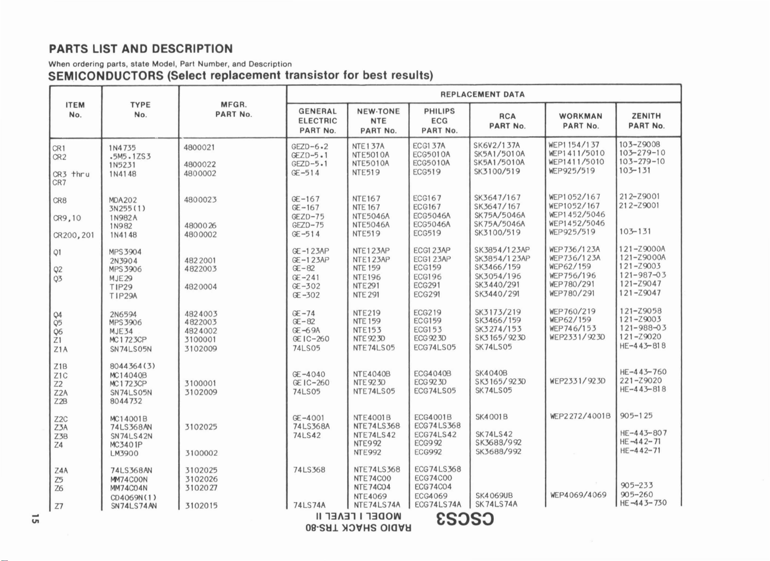
PARTS LIST AND DESCRIPTION
When ordering parts, state Model, Part Number, and
Description
SEMICONDUCTORS (Select replacement transistor for best results)
VI
ITEM
No.
CRI
CR2
CR3
thru
CR7
CR8
CR9,10
CR200,201
Ql
Q2
Q3
Q4
Q5
Q6
ZI
ZlA
ZIB
ZlC
Z2
Z2A
Z2B
Z2C
Z3A
Z3B
Z4
Z4A
Z5
Z6
Z7
TYPE
No.
1N4735
.5M5.
1ZS3
lN5231
lN4148
MOA202
3N255(1)
1N982A
lN982
lN4148
MPS3904
2N3904
MPS3906
MJE29
T1P29
TIP29A
2N6594
MPS3906
MJE34
MCl723CP
SN74LS05N
8044364(3)
MC14040B
MCI723CP
SN74LS05N
8044732
MC14001B
74LS368AN
SN74LS42N
MC3401P
LM3900
74LS368AN
MM74COON
MM74C04N
CD4069N(
SN74LS74AN
REPLACEMENT
MFGR.
PART No.
4800021
4800022
4800002
4800023
4800026
4800002
4822001
4822003
4820004
4824003
4822003
4824002
3100001
3102009
3100001
3102009
3102025
3100002
3102025
3102026
3102027
1)
3102015
GENERAL
ELECTRIC NTE
PART
No.
GEZD-6.2
GEZD-5.1
GEZD-5.1
GE-514
GE-167
GE-167
GEZD-75
GEZD-75
GE-514
GE-123AP
GE-123AP
GE-82
GE-241 NTE196
GE-302
GE-302
GE-74
GE-82
GE-69A
GE
IC-260
74LS05
GE-4040
GE
IC-260
74LS05
GE-4001
74LS368A
74LS42
74LS368
74LS74A
NEW·TONE
PART No.
NTE137A
NTE5010A
NTE5010A
NTE519
NTE167
NTE167
NTE5046A
NTE5046A
NTE519
NTE123AP
NTE123AP
NTE
159
NTE291
NTE291
NTE219
NTE159
NTE153
NTE9230
NTE74LS05
NTE4040B
NTE923D
NTE74LS05
NTE4001B
NTE74LS368
NTE74LS42
NTE992
NTE992
NTE74LS368
NTE74COO
NTE74C04
NTE4069
NTE74LS74A
II 13J\31 I 13COW
09'S~:U
)t~VHS
OICVij
PHILIPS
ECG
PART No.
ECG137A
ECG5010A
ECG5010A
ECG519
ECG167
ECG167
ECG5046A
ECG5046A
ECG519
ECG123AP
ECG123AP
ECG159
ECG196
ECG291
ECG291
ECG219
ECG159
ECG153
ECG923D
ECG74LS05
ECG4040B
ECG923D
ECG74LS05
ECG4001B
ECG74
LS368
ECG74LS42
ECG992
ECG992
ECG74
LS368
ECG74COO
ECG74C04
ECG4069
ECG74LS74A
ESOSO
SK6V2/137A
SK5Al/5010A
SK5A1/5010A
SK3100/519
SK364
SK36471167
SK75A/5046A
SK75A/5046A
SK3100/519
SK3854/123AP
SK3854/123AP
SK3466/159
SK3440!291
SK3440/291
DATA
RCA
PART
No.
7/16
7
SK3054/196
SK3173!219
SK3466/159
SK3274/153
SK3165/923O
SK74LS05
SK4040B
SK3165/923D
SK74LS05
SK4001B
SK74LS42
SK3688/992
SK3688/992
SK4069UB
SK74LS74A
WORKMAN
PART
No.
WEPI
154/1
WEP1411/5010
WEP1411/5010
WEP925/519
WEP1052/167
WEP1052/167
WEP1452/5046
WEP1452/5046
WEP925/519
WEP736/123A
WEP736/123A
WEP62/159
WEP756/196
WEP780!291
WEP780/291
WEP760!219
WEP62/159
WEP746/153
WEP2331
WEP2331
WEP2
WEP4069/4069
37
1 9230
19230
272/4001
ZENITH
PART
103-Z9008
103-279-10
103-279-10
103-131
212-Z9001
212-Z9001
103-131
121-Z9000A
121-Z9000A
121-Z9003
121-987~3
121-Z9047
121-Z9047
121-Z9058
121-Z9003
121-988~3
121-Z9020
HE-443-818
HE-443-760
221-Z9020
HE-443-818
905-125
B
HE-443-807
HE-442-71
HE-442-71
905-233
905-260
HE-443-730
No.
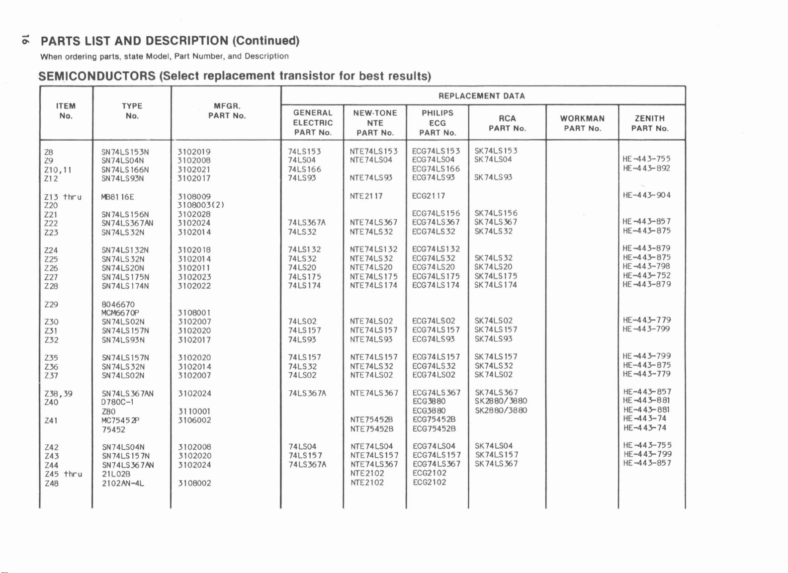
0:
PARTS LIST AND DESCRIPTION (Continued)
When ordering parts, state Model, Part Number, and Description
SEM.ICONDUCTORS (Select replacement transistor for best results)
ITEM TYPE
No. No.
Z8
Z9
Z10,11
Z12 SN74LS93N
Z13
thru
Z20
Z21
Z22
Z23
Z24
Z25
Z26
Z27
Z28
Z29
Z30 SN74LS02N
Z31
Z32 SN74LS93N
Z35 SN74LS157N
Z36 SN74LS32N
Z37
Z38,39
Z40
Z41
Z42
Z43
Z44
Z45
thru
Z48
SN74LS153N
SN74LS04N
SN74LS 166N
M::I8116E
SN74LS156N
SN74LS36
SN74LS32N
SN74LS132N
SN74LS32N
SN74LS20N
SN74LS175N
SN74LS 174N
8046670
MCM6670P
SN74LS157N
SN74LS02N
SN74LS367AN
D780C-l
Z80 3110001
MC75452P
75452
SN74LS04N
SN74LS 157N
SN74LS367,4.N
21L02B
2102AN-4L
7,4.N
PART
3102019
3102008
3102021
3102017
3108009
3108003(2)
3102028
3102024
3102014
3102018
3102014
3102011
3102023
3102022
3108001
3102007
3102020
3102017
3102020
3102014
3102007
3102024
3106002
3102008
3102020
3102024
3108002
MFGR.
No.
GENERAL
ELECTRIC
PART No.
74LS153
74LS04
74LS
166
74LS93
74LS367A
74LS32 NTE74LS32
74LS132
74LS32
74LS20
74LS175
74LS 174
74LS02
74LS 157
74LS93
74LS 157
74LS32
74LS02
74LS367A
74LS04
74LS157
74LS367A
NEW·TONE
NTE
PART No. PART No.
NTE74LS153
NTE74LS04
NTE74LS93
NTE2117 ECG2117
NTE74LS367
NTE74LS132
NTE74LS32
NTE74LS20
NTE74LS175
NTE74LS 174
NTE74LS02
NTE74LS 157
NTE74LS93
NTE74LS 157
NTE74LS32
NTE74LS02
NTE74LS367
NTE75452B
NTE75452B ECG75452B
NTE74LS04 ECG74LS04
NTE74LS157 ECG74LS157
NTE74LS367
NTE2102
NTE21
02
REPLACEMENT
PHILIPS
ECG
ECG74LS 153
ECG74
LS04
ECG74LS
ECG74LS93
ECG74LS
ECG74LS367
ECG74LS32
ECG74LS132
ECG74LS32
ECG74
ECG74LS175
ECG74LS 174
ECG74LS02
ECG74LS 157 SK74LS 157
ECG74LS93
ECG74LS 157
ECG74LS32
ECG74LS02
ECG74LS367
ECG3880
ECG3880
ECG75452B
ECG74LS367
ECG2102
ECG2102
166
156
LS20
DATA
RCA
PART No.
SK74LS 153
SK74LS04
SK74LS93
SK74LS156
SK74LS367
SK74LS32
SK74LS32
SK74LS20
SK74LS175
SK74LS174
SK74LS02
SK74LS93
SK74LS 157
SK74LS32
SK74LS02
SK74LS367
SK2880!3880
SK2880!3880
SK74LS04
SK74LS157
SK74LS367
WORKMAN
No.
PART
ZENITH
PART
No.
HE-443-755
HE-443-892
HE-443-904
HE
-443-85
HE-443-875
HE-443-879
HE-443-875
HE-443-798
HE-443-752
HE-443-879
HE-443-779
HE-443-799
HE-443-799
HE-443-875
HE-443-779
HE-443-857
HE-443-881
HE-443-881
HE-443-74
HE-443-74
HE-443-755
HE-443-799
HE-443-857
7

PARTS LIST AND DESCRIPTION (Continued)
When ordering parts, state Model, Part Number, and Description
SEMICONDUCTORS (Select replacement
ITEM TYPE MFGR.
No.
Z49
Z50
Z51
Z52
Z53
Z54
Z55
Z56
Z57
Z58 SN74LS92N
Z59
Z60
Z61
thru
Z63
Z64 SN74LS 157N
Z65 SN74LS93N
Z66
Z67,68
Z69,70
Z72
Z73
Z74
Z75,76
No.
SN74LS157N
SN74LS93N
SN74LS 157N
SN74LS04N
SN74LS 132N
SN74LS30N
SN74LS367AN
SN74LS92N
M'174C04N
CD4069CN( 1)
SN74LS 175N
SN74LS36
21L02B
2102AN-4L
SN74LSllN
SN74LS36
SN74LS74AN
SN74LS36
SN74LS32N
SN74LSOON
SN74LS367AN
7AN
7AN
7AN
3102020
3102017
3102020
3102008
3102018
3102013
3102024
3102016
3102027
3102016
3102023
3102024
3108002
3102020
3102017
3102010
3102024
3102015
3102024
3102014
3102006
3102024
PART No.
transistor
GENERAL
ELECTRIC
PART No.
74LS157
74LS93
74LS157
74LS04
74LS
132
74LS30
74LS367A
74LS 175
74LS367A
74l..S
157
74LS93
74LSll
74LS367A NTE74LS367
74LS74A
74LS367A NTE74LS367
74LS32
74LSOO
74LS367A
for
best results)
NEW·TONE
NTE ECG
PART No.
NTE74LS
NTE74LS93
NTE74LS157
NTE74LS04
NTE74LS132
NTE74l..S30
NTE74LS367
NTE74C04
NTE4069 ECG4069
NTE74l..S 175
NTE74LS367
NTE2102
NTE2102
NTE74LS 157
NTE74LS93
NTE74l..S11
NTE74LS74A
NTE74LS32
NTE74LSOO
NTE74LS367
REPLACEMENT DATA
PHILIPS
PART No.
ECG74LS
157
ECG74LS93
ECG74LS 157
ECG74LS04
ECG74LS132
ECG74LS30
ECG74LS367
ECG74LS92
ECG74C04
ECG74LS92
ECG74LS 175
ECG74LS367
ECG2102
ECG2102
ECG74LS 157 SK74l..S157
ECG74LS93 SK74LS93
ECG74l..S11
ECG74LS367
ECG74
ECG74LS367
ECG74LS32
ECG74LSOO
ECG74
157
LS74A
LS367
RCA WORKMAN
PART No.
SK74LS 157
SK74LS93
SK74LS157
SK74LS04
SK74LS30
SK74LS367
SK4069UB
SK74LS 175
SK74LS367
SK74l..S11
SK74LS367
SK74LS74A
SK74LS367
SK74LS32
SK74LSOO
SK74LS367
PART No. PART No.
HE-443-799
HE-443-799
HE-443-755
HE-443-879
HE-443-732
HE-443-857
905-233
WEP4069/4069
905-260
HE-443-752
HE-443-857
HE-443-799
HE-443-864
HE-443-857
HE-443-730
HE-443-857
HE-443-875
HE-443-728
HE-443-857
ZENITH
.....
(1)
NumberonunIt.
(2)
Used
(3)
2e~.
In
4K
8044732
versIons.
used
In
pJ~ce
of
8044364
In
e~rly
versIon
II 131\31 I
OS-SI:t.l
of
LevelII.
>lO"HS
1300W
OIO"1:t
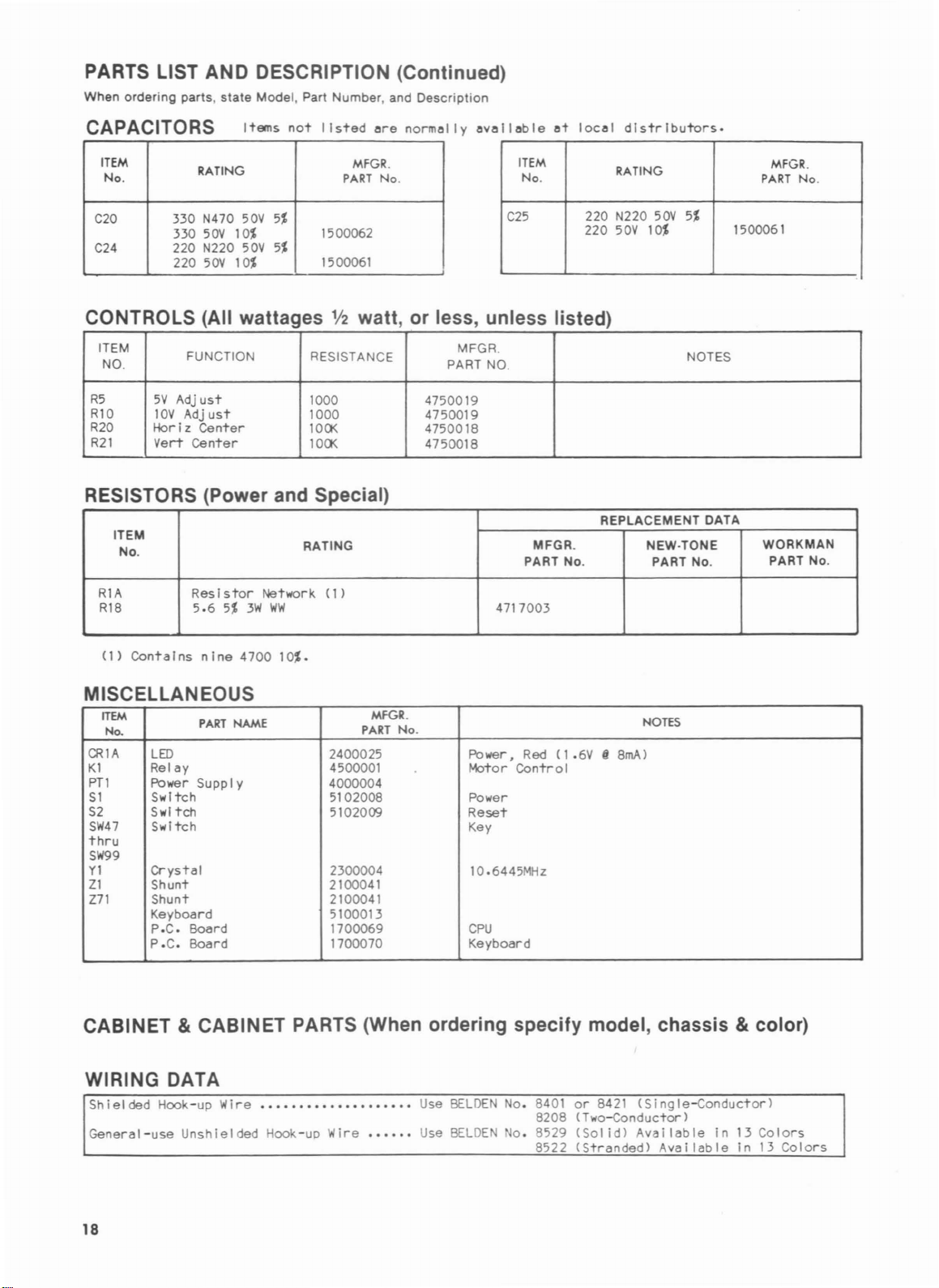
PARTS LIST AND DESCRIPTION (Continued)
When ordering parts, state Model, Part Number, and
Items
not
CAPACITORS
listed
Description
~re
norm~1Iy~v~ll~ble~t10c~1
distributors.
ITEM
No.
C20
C24
RATING
330 N470 50V
330
50V
50V
10%
50V
10%
220 N220
220
5%
5%
CONTROLS (All wattages
ITEM
NO.
R5
Rl0
R20
R21
5V
10V
Horiz
Vert
FUNCTION
Adj
ust
Adj
ust
Center
Center
MFGR.
PART
1500062
1500061
Y2
watt,
RESISTANCE
1000
1000 4750019
lOa< 4750018
lOa<
RESISTORS (Power and Special)
R1A
R18
ITEM
No.
Res I
5.6
stor
5%3WWW
Network
RATING
(ll
No.
ITEM
No.
C25
or
less, unless listed)
MFGR.
PART NO.
4750019
4750018
MFGR.
PART No.
4717003
RATING
220 N220
220 50V
REPLACEMENT DATA
50V
5%
10%
NOTES
NEW·TONE
PART No.
MFGR.
PART
1500061
WORKMAN
PART No.
No.
(1)
Contains
nine
4700
10%.
MISCELLANEOUS
ITEM
No.
CR1A
Kl
PTl
Sl
S2
SW47
thru
SW99
Yl
Zl
Z71
PART
LED
ay
Rei
Power SuppI y
Switch
Swl
tch
Switch
Crystal
Shunt
Shunt
Keyboard
P.C.
Board
P.C.
Board
NAME
MFGR.
PART
No.
2400025
4500001
4000004
5102008 Power
5102009
2300004
2100041
2100041
5100013
1700069
1700070
Power,
Motor
Reset
Key
10.6445MHz
CPU
Keyboard
CABINET & CABINET PARTS (When ordering
WIRING DATA
Use
Use
BELDEN
BELDE
Shielded
General-use
Hook-up
Unshielded
Wire
Hook-up
Wire
••••••
Red(1.6V 118mA)
Control
specify
No.
8401
8208
o.
8529
8522
model, chassis & color)
or
8421
(Two-Conductor)
(Sol
(Stranded)
NOTES
(Single-Conductor)
id)
Avai
lable
Avai
in13Colors
lable
in13Colors
18
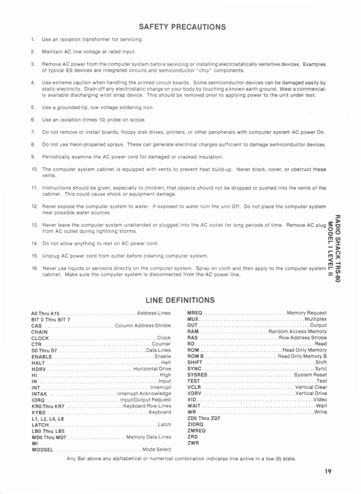
1.
Use an
isolation
2.
Maintain AC line voltage at rated input.
3.
Remove AC power from the
of
typicalESdevices are integrated
4.
Use extreme
static
electricity.
ly available
5.
Use a grounded-tip, low voltage soldering iron.
6.
Use an
isolation
7.
Do
not
removeorinstall
8.
Do
not
use freon·propelled sprays. These can generate
transformer
caution
discharging
when handling the printed
Drain
(times
for
servicing.
computer
off
any
electrostatic
wrist
strap device. This should be removed
10)
probe on scope.
boards, floppy
SAFETY PRECAUTIONS
system before servicingorinstalling
circuits
and
semiconductor
circuit
boards. Some
charge on
disk
drives, printers,orother
your
electrical
body by
"chip"
touching
charges
electrostatically
components.
semiconductor
a known earth ground. Wear a commercial-
priortoapplying powertothe
peripherals
with
sufficienttodamage
sensitive devices. Examples
devices can be damaged easily by
unit
computer
systemACpower On.
semiconductor
under test.
devices.
9. Periodically examine the AC power cord
10.
The
computer
vents.
11.
Instructions
cabinet. This could cause
12.
Never expose the
possible
near
13.
Never leave the
from AC
14.
Do
not
15.
Unplug AC power cord from
16.
Never use
cabinet. Make sure the
system
should be given, especiallytochildren, that
water sources.
outlet
allow anythingtorest on AC power cord.
liquidsoraerosols
cabinet is equipped
computer
computer
during
lightning
computer
shock
systemtowater. If exposedtowater
system unattended or plugged
storms. g0
outlet
directly
for
damagedorcracked insulation.
with
ventstoprevent heat build-up. Never block, cover,orobstruct
or equipment damage.
before cleaning
on the
computer
system is
disconnected
LINE DEFINITIONS
AO
Thru A
15
BIT
0 Thru BIT 7
CAS Column Address Strobe
CHAIN
CLOCK
CTR
DO
Thru 07 Data Lines
ENABLE Enable
HALT Halt
HORV Horizontal Drive
HI High
IN
INT Interrupt
INTAK Interrupt Acknowledge
IORC
KRO
Thru KR7 Keyboard Row Lines
KYBO Keyboard
L2,
L4,
L1,
LATCH Latch
LBO
MOO
MI
MOOSEL . . . . . . . . . .
La
Thru LB5
Thru
M07
..
. Mode Select
Any Bar above any alphabetical
Address Lines
Clock
Counter
Input
1npuUOutput Request
Memory Data Lines
or
numerical
objects
into
the AC
computer
system.
system. Spray on
from
MREC Memory Request
MUX
OUT
RAM Random Access Memory
RAS Row Address Strobe
RD
ROM
ROM B Read Only Memory B
SHIFT
SyNC
SYSRES System Reset
TEST Test
VCLR Vertical Clear
VORV Vertical Drive
VIO
WAIT Wait
WR
ZOO
ZIORC
ZMREC
ZRO
ZWR
combination
these
should
not
turn the
outlet
be dropped or pushed
unit
Off. Do not place the
for
long periods of time. Remove AC plug
into
the ventsofthe
computer
system
3:
men
'::x:
-:J>
'0
m"
cloth
and then applytothe
the AC power line. =
•.............................
Thru
Z07
indicates line active in a low
(0)
Read
state.
computer
Only
system,
Multiplex
Memory
~-1
Output
Read
Shift
Sync
Video
Write
::D
:J>
C
::D
~
o
19
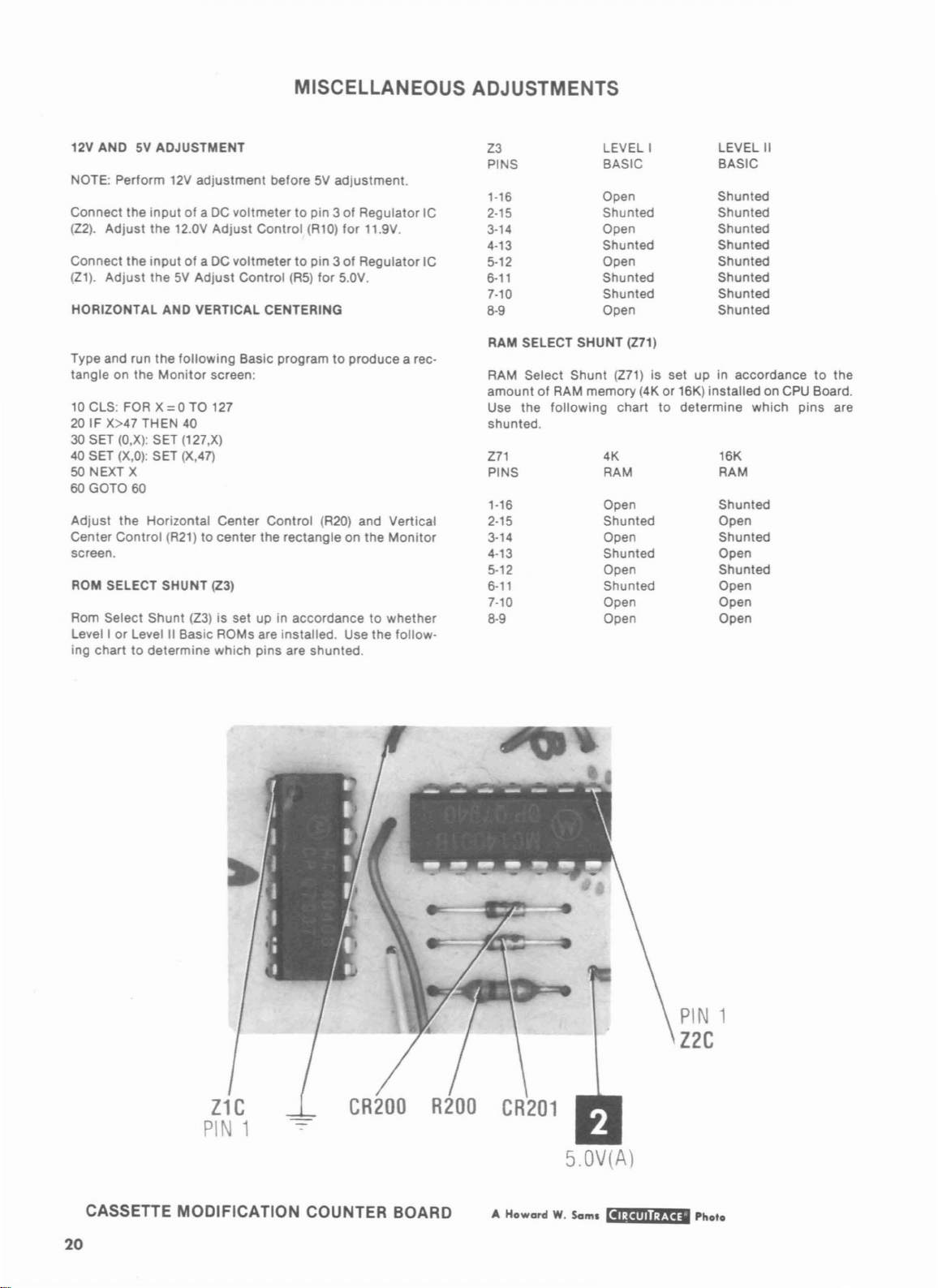
MISCELLANEOUS ADJUSTMENTS
12V
AND5VADJUSTMENT
NOTE: Perform
Connect the inputofaDCvoltmetertopin 3ofRegulator IC
(Z2).
Adjust
Connect the
(21).
Adjust
HORIZONTAL AND VERTICAL CENTERING
12V
adjustment before5Vadjustment.
the 12.0V
inputofaDCvoltmetertopin 3ofRegulator IC
the5VAdjust
Adjust
Control (Rl0) for 11.9V.
Control
(R5)
for 5.0V.
Z3
PINS
1·16
2-15
3-14
4·13
5-12
6·11
7-10
8-9
LEVEL I
BASIC
Open
Shunted Shunted
Open
Shunted
Open Shunted
Shunted
Shunted Shunted
Open Shunted
LEVEL
BASIC
Shunted
Shunted
Shunted
Shunted
II
Type and run the following Basic program to produce a rec·
tangle on the
10
CLS: FOR X =0 TO
20
IF X>47 THEN
30
SET
40
SET
50
NEXT X
60
GOTO
Adjust
Center Control
screen.
ROM
SELECT SHUNT (23)
Rom Select Shunt
Level IorLevelIIBasic ROMs are installed. Use the follow·
ing chart to determine which pins are shunted.
Monitor
(O,X):
SET (127,X)
(X,O):
SET (X.47)
60
the Horizontal Center Control
screen:
127
40
(R21)
to center the rectangle on the
(Z3)
is set up in accordance to whether
(R20)
and Vertical
Monitor
RAM SELECT SHUNT (271)
RAM Select Shunt
amountofRAM memory
Use the following chart to determine which pins are
shunted.
Z71
PINS
1-16
2-15
3-14
4-13
5-12
6-11
7-10
8-9
(Z71)
Is set up in accordancetothe
(4K
or 16K) installed on
4K
RAM
Open
Shunted Open
Open Shunted
Shunted Open
Open Shunted
Shunted
Open
Open Open
16K
RAM
Shunted
Open
Open
CPU
Board.
CASSETTE MODIFICATION COUNTER BOARD
20
A
Howard
5.0V(A)
W.
Sam.
PIN
Z2C
lilii·AIIii-d31
1
Photo

1
2
3 4
5
6
7
8
9
10
11
12
13
14
15
16
17
18
19
20
21
22
23
24
25
26
1
27
28
29
30
A
B
C
D D
E
A
B
C
E
F F
G
H
G
H
::tJ
3:»
2
0
cO
mC/)
r-~
-»
r-C')
m",
<-4
~::tJ
_C/)
-CD
0
J
K
L
M
N
1
CPU
BOARD A Howord W.
12
2
3
4
SamslC;@.UUaWPhoto
5
6
7
8
9
10
11
12
13
14
15
16
17
18
19
20
21
22
23
24
25
26
27 28
29
CPU BOARD
J
K
L
M
N
30
21

PIN
Z4
1
P 1
P 1
Z8
Zll
PI
1 P 1
PI
Z12 Z13 Z15
1
PI
1
pI
Z16
Z17
1
PI
Z2
1
PI
1
Z19
PI
Z20
1 P 1
Z38
PI
Z39
1
PI
N 1
Z22 Z23
PI
N 1
PI
N 1
255
PI
240
1
(')
CJ)
(')
CJ)
CN
CPU BOARD
22
Z42 Z43 Z25 Z44
P 1 P P 1 P
\
1
p
P
Z51
~
272
P "
Z36 Z73
PI
1
PI
1
CPU BOARD
11

::D
3:>
2
0
cO
men
....
::I:
->
....
0
m"
<~
~::D
_en
-~
o
Z56
PIIIJ
CPU BOARD A
10
1
HowardW.Sam,
'IUAiiiI.f.i3i
Photo
CPU BOARD
23

LOGIC CHART
PIN
2
3
5
6
7
8
9
PIN
2 L H
3 L
5 L P
6 L H H L H
7 L
8 L
IC
NO.
Zl
(ll
1
4 L 4
10
11
12
13
14 H
IC
NO.
Z2C
1
H P
4
H H H
PIN
IC
NO.
ZlA
P 1
L 2 P
P
3
P
5 P
L 6
L 7
L
8 P 20
P 9 P
L 10 P 22 P
P
11
12
L
P
IC IC IC
Z3A
Z3B
P
H
H
P
IC
Z18
P 13 P
P
P
P
P
P
L
Z4
L P
L H
L P P P
P
H P P P
P H
L L L L
L P L
PIN
NO.
21
23 P
24
Z4A
H
IC
PIN
Z18
NO.
ZlC
1
14
P 2
15
P
16
P
17
P
18
P
19
L 7
P
P
H 12
IC
IC IC
Z5
P P H L L L L P P
P
P
P
P
L
L L
3 L
4 L L
5
L P
6 L L 6
L L 7
8
L L 8
9
L P 9 P
10
P L
11
H
L L 12 L 24 H
13
L
14 L H
15
L
H
16
Z6
Z7
P L P H L L P P
P
P H P
P L
P H P H L L
L L
P H L
IC
IC
IC IC IC
Z2A
Z2
(1)
P 1
P 3 P
P
P
Z8 Z9
P P L L
P P P
P L P P
L P
P
P L
IC
PIN
NO.
2 P 14 P
4 P
5 P
10 P 22
11
IC
Z10
IC
PIN
NO.
Z28
P 13 P
15
16
17
P
18
P
P 20 H
P
P
19
21
23 P
IC
Zll
IC
Z12 Z13
P
P P
H
P
P
L P H
IC
Z2B
P
P
P
P
L
H
P
IC
P
P
P
P
9 L P
10 H
11
L P P
12 H P
13 L P L L
14 H P L
15
16
Logic probe readings taken
keys pressed, unless otherwise noted.
Logic Probe Display
L=Low
H
P
H
H
P
L P P P
P L
H
P P P
H H H
with
computer
H = High
p=
Pulse
*= Open (No
(1)
Logic readings not taken
light
On)
P P
P
P
H
P P P
P P P
P H
turned On, no
H P P H H P H
P L
L P L P P P
L P H
L P L P L P
H H
.H
H P P L P
P
P
P H
L P H P
L P P P
H H
P
P
P
L
P
P
24

LOGIC CHART (Continued)
PIN IC IC
NO.
1 P
2
Z15
Z14
P P P P
P P
P
3 P P
4 P P
5 P P P
IC
Z16
P P
P P
IC
Z17
P
P
IC
IC IC
Z18 Z19
P P
P
P
P P P
Z20
P P
P
P P P
P P P P P L
IC IC IC IC
Z21
P P P P
P
H P
Z22 Z23 Z24
H H P L
H H
P
L
P
Z25 Z26
L P
L
H L H
H
IC
IC
P
P
P P
6 P P P P P P P H P P H H H P
7
P P P P P
8 H
9 H H
10
11
12
13
14
15
16
PIN
NO.
H
H H H
P P P P P
P P P P P
P
P P
P P P
P
L L L
IC
Z28
H
P P P P
P P
P
P P
IC
IC IC
Z29
Z30
1 H P P
2 P P L P
3 P P P
P P H
4
P
5
6 P
7
~
8 L
P
9
10
P P
P
11
12
P P P P
L P H P P P P P 5 L 25
P
P
L
L P
P
P
P
P P P P H P L
L
P P
L
P
H
H
P P P
P
P P P P
P P
L L L L
Z31
H P P P H L L 1 P
P P P
P
P
L
P
IC
Z32
P P
*
*
*
P
L P
P
P P P
P H P L L L L
P
H
H L L H
H
H
P P
P P P
P P P
P P L P
IC
IC IC
Z36
Z35
H
H L L
P
P P P P
P P P P
P
L L P P 7 P
L H
P
P P L P
H
P
H H
P
P
P P
P P
P
H
H
IC IC
Z37
Z38 Z39
L L
P
L L 8
L L P
L
P P
L
P H H P
P
P
H
H
L L P
H
H H
PIN
NO.
P
2
P
3 P
4 P 24 H
P
6 P 26 H
9
P
10
P
11
12
H P L
H H P
L P P
L P P
H P
H
PIN IC
IC
Z40
NO
21
22 P
P
23
27
P
28
P
29
P 30 P
H
31
P 32
IC
Z27
H
H
L
P
P
P
H
Z40
P
H
H
P
P
L
P
P
:::D
~»
52
0
cO
mC/)
1:1:
-»
10
m"
<~
~:::D
_C/)
-0,
o
13
P P P
P P H
14
15
P
16
H
17
18
Logic
probe
keys pressed,
Logic
Probe
L=Low
H =
High
P=
Pulse
* =Open (No
P
P
P H H H H
L
H
readings
unless
Display
light
taken
otherwise
On)
P P
L
with
noted.
computer
*
turned
P L H
P
H H
L
On,
no
P P
P P
L L
13
14
15
16
17
18
19
20
P
33 P
34
P
P
35
L 36
H
37
H
38
39
P
H 40 L
P
P
P
P
P
P
25

LOGIC CHART (Continued)
PIN
NO.
1 L P H H
2 L
3 H P P
4
5 P
6 P P
7 P
8
9 H P P L
10
12
13
14
15
16
PIN
NO.
1 P P
2
3
4
IC
IC
Z41
Z42
P P P P
L P P P P
P L
P P P
L P
H
L L L
H
11
IC
Z55
P
P
P
P P H H H
L P P
H P L
L
H P H
L H P
H
IC IC IC
Z56
P P
P
*
*
P
*
IC
Z43
P
Z57
P
IC IC IC
Z44
Z45
Z46
P P
P P P P P P
P H H
P P
P P P
P P
P L L
P
P
P
P P
L L L
P P
P P
P
P P P P P P
P
H
P
P P P
IC IC IC
Z58 Z59
*
*
*
Z60
H H P
L
L P
H P H H H
P
P P P P P
5 P H P H P P P
6 P
7
8 L P P P
L P L
P
L L L L
H P
L
P
L
IC IC IC
Z48 Z49
Z47
P P
H H
P
P P
P P
H P P
P P L H L
P P
P P
H
H
P L P
P P
P L P
H
P
P P P P
P
L L
P
Z61
H P H
P
H
L L
P
H H
IC IC IC IC IC IC
IC
Z62 Z63 Z64 Z65 Z66
P P
P P
P P
P P P P
P
P P
P
P P L P
IC
Z50
P
*
H P
P
*
*
L
*
H P P P
P L
P L
*
IC IC IC
IC
Z52
Z51
L
H
L
P
P P P
P L L L
H P H
P L P
H P
L L
P H
P P H
H H H
P P P
P
P P
P H P
P P
*
P
*
L P P
P L L
Z54
Z53
H P
H
P
P
H P
P P
*
*
P
P
*
Z67 Z68
P
P
P
P
P
P
P
9 P P P
P
10
11
12
13
14
15
16
PIN
NO.
1
2
3
4
5
L P L
P P P P H L P
H P
P
P
*
P H
L
H
IC
IC
Z69
Z70
p
P P
P
P P
P
H
H
P
P
6 P P
L L
7
8 P P
P P
9
10
11
12
13
14
H
P P
P P
P
H H
H
H L
15
16
P
P
P
*
H
P H
IC
IC
Z73
zn
H P
L
P
P
H
L
P
P
P
P
L
L L
P P
L
P P
P H
P
H P P P
P
P H
H P
L H
L
H H
H
P L L L P P P P P
L
P H H H
P
P L P P L P P
P L L
L P P P
L L
H
IC IC
Z74 Z75
P P
P
P
P
P P
L
P
P P
H
P
P P
P P
P P
P
L
P P
P P
P
P P P
IC
Z76
P
P
P
P
L
P
P
L L
P P L H L
Logic probe readings taken
no
On,
Logic Probe Display
L=Low
H = High
P= Pulse
keys pressed, unless
* =Open (No
L P P P
P
P P
P
*
P P
H
light
On)
P P
H
P
P
P
P
H
P
L L
P L L
P P P
H P
H H
with
computer
otherwise
noted.
P
turned
26

TERMINAL GUIDES &
Ie
PINOUTS
I
I
I
4
~
6
7
CI.fAR
lQ
10
10
20
20
2Q
GHO
GNO
511741.$17511
ClRP----..o1~.qClR
CK
4>--r-+--<:t>CK
ClRP--+~~.qClR
o
CK
4>----i----<P
Q
m,m
fliPIFLOP
TOP
VIEW
SH7US367AH
SH74LSI56Il
vee
16
I~
STR08E
14}INPUTS
13
12
OUTPUT
INPUTS
III
10
9
OUTPUT
16
I~
14
OUTPUTS
OUTPUTS
PARAlLEL
INPUTS
ClOCK
INHI81T
ClOCK
I
3
4
~
7 6
GNO
r--<
r-<
r
vee
16
4Q
I~
Q
40
U
ij
40
13
'------;12
L..-------lll
L..------.410
vee
4A
48
4Y
3A
235,
243
ZSl.
264
VIEW
'-----..0113
30
2
3-
11
Q
3
Q
16
I~
9
ClOCK
10
9
8
GNO
OUTPUTS
CK
vee
~
4Y
IY2
~----<1IY2
61"1_Y!~_--<11Y1
71"1",YO'-_--<1IYO
I
GNO
SH74LS36IAH
A~---+-iA
vee
16
,-------ll~
DECODER
TOP
u
13
12
11
10
Z21
VIEW
SELECT
OUTPUT
INPUTS{:
OUTPUT
INPUTS{:
I
4
7
8
GNO
231.
IIULTIPLEXER
SlI74LSmH
IA
18
lY
2A
28
249.
TOP
SH74LSI66H
A
OH
7
238
SHIfT
VIEW
lIO.
REGISTER
TOP
A
8
C
L..----f9
Z1I
VIEW
vee
r----l
,------
r--
I
GNO
SH74LS42H
0 I
I
2
3
4 0
5
7
8
9
DECODER
TOP
vee
14
13
12]
11IPUTS
10
I
I
I
1
1
9
16
I~
~~~I
PARAlLEL
INPUT
PARAlLEL
OUTPUT
PARAlLEL
ClEAR
IHPUTS
DATA
INPUTS
OUTPUT
I
I----
I---
He
vee
He
NC
INPUT
lI2.
IG
STR08E
8
SELECT
7
SN74LS93N
8
1 1
B
ROW
Rom
OC
232.
COUHTER
TOP
VIEW
2SO.
IC2
ICI
ICO
IY
INPUT
X
OA-I
00-1
08,--
265
B
f-
1------..----+----lA
At------
A
NC
GNO
.........
-+--+---fB
IIULTIPLEXER
TOP
1
I
I
74LS153N
21
VIEW
t--+..:;A:.,:SE:o:L:::EC:,:T---l
.........
--lA
2G
2G
2C3
2C2
2C1
2CO
2Y
27.269.270
fliPIFLOP
TOP
VIEW
STR08E
071OC·1
,AIO
~2~
!lrolii
VIEW
A9
A8
A7
A636
AS
A4
A3
A2
AI
AD
GNO
mil
iI
RESET
WAIT
WR
Rli
40
39
38
26
24
23
22
37
3~
34
33
32
31
30
29
28
27
21
8
GNO
Z2I
fllPlfLOP
TOP
VIEW
3:>
0
cO
men
r-z
>
r-O
m;:ll;
::D
2
vee
16
I~
14
13
12
11
10
9
DATA
INPUTS
OUTPUT
All
A12
3
Al3
4
AU
~
AI~
6
ClK
7
04
8
03
9
3~
10
06
11
~V
12
02
13
07
1400
I~
01
16
jjjJ
11
lOO
18
HAlT
19
liIl£ll
20
fORO
MICROPROCESSOR
TOP
240
<-4
~::D
=en
Co
o
l22, 13l,
l39,
,l
B
260,
Z75,
8UffER
VIEW
zsa
VIEW
1
A
Z67,
Z76
244,
26&,
~1
~I
~9
~I
m,
m.
TRI,STATE
TOP
SlI74U92H
1 I
2
HC
HC
HC
vee
IHPUT IHPUT
ROW
ROm
Z56,
DIVIDE8Y6.
DIVIDE8Y12
TOP
3
4
~
61---71---
6
Hel
GNO
23A,24A
TRISTATE
INVERTER
TOP
VIEW
IICI4040ll
VOO
Qll
QIO
Q8
Q9
RESET
jfi
Ql
E B C
16
15
14
13
12
11
10
9
I
Q12
2
IIC7~~2P
241
I
DRIVER
lOP
VIEW
WIOENT
Q6
3
Q~
4
Q7
~
Q4
6
Q3
7
Q2
I
VSS
ZlC
COUNTER
TOP
VIEW
G
QI.
Q2.
JlA,
fRONT
II.
J3
VIEW
80nOll
Q4
VIEW
8CE
fRONT
Q6
VIEW
80nOll
Q5
VIEW
1188116E
1
V88
2
DIN
3
WI:
4
RAS
~
AD
6
A2 A4
7
AI
I
YOO
ZI3
THRU
RAIl
TOP
VIEW
~IOENT
8CE
Q3
fRONT
VIEW
Z20
VSS
CAS
OOUT
A6
A3
A~
vee
8046670
16
15
14
13
12
II
10
9
I
A6
2
A~
3
A4
4
A3
~
A2
6
Al
7
AD
I
RSJ
9
GNO
CHARACTER
TOP
vee
cs
04
03
02
01
00
RSI
RS2
Z29
GENERATOR
VIEW
II
17
16
I~
14
13
12
II
10
J
QI
2
T.t
3 K
RESET
6
CLK
7
PIS
8GNO
m
261
TOP
21L028
THRU
THRU
RAIl
VIEW
l4I.
Z63
VOO
Q2
Q3
Q4
PI4
PI3
PI2
PIl9
16
I~
14
13
12
II
10
1
NC
CURRENT
2
LIMIT
3
CURRENT
SENSE
4
INVERTING
INPUT
~
NON
INVERTlHG
INPUT
6
¥REf
7
V-
IICI7Z3CP
NC
14
CO~~~~~:'
V+
Yell
VOUT
13
12
10
vz
NC
lI.22.
REGULATOR
TOP
VIEW
I
13
}
11
l[]"
•
II
5
10
• •
1 •
lIA,
l2A,
24. 29.
223.
m,
225.
Z2fi,
230. 236. 237,
242.
ZSl.
ZSJ,
~,266,
273,
214,
TOP
VIEW
I
13
}
•
5
• •
1 I
Z2C
TOP
VIEW
11
II
10
I[]"
I
100
}
•
5
• •
, 0 I
ZS,
26,
Z57
TOP
VIEW
13
l'
11
II
10
2 3 4 5 6 1 8
RIA
fRONT
VIEW
liB,
TOP
Z2I
VIEW
27
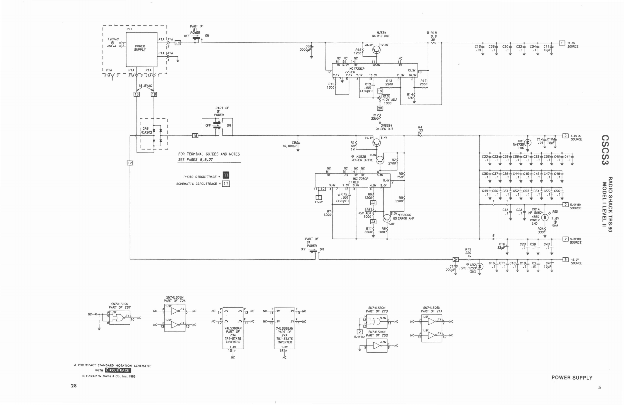
I
I
120VAC
I
@
400
I
I
I
I
I
PIA
JIAYS
PTI
00\
POIiER
5~lY
- - I
PIA
PIA
I
1"104
~
2
1
JIA
h
4
1
1
_
I
I
CR8
/()A202
17
+--.------118
....J
..
FOR
SEE
PART
51
POWER
a'F
-
...
"'"
TERMINAL
PAGES
a'
OH
L---------------------r--r-------r-:;;;~
PART
a'
51
POWER
.......--........
cs
10,OOOJJF
GUIDES
AND
NOTES
6,9,27
OS
ItJE34
RES
..
Q4
OUT
2N6S94
RES
OUT
2700
R2
R4
.33
211
e
R18
5.6
31/
11.9Y
SCUlCE
o
CJ)
o
CJ)
CN
He~HC
I
J,
A PHOTOPACT STANOARD
WITH
© Howard
28
W.
SH?4l502N
PART
a'
Z37
10
NOTATION
""·i'ini·f.iM'
Sama & Co., Inc.
1985
SCHEMATIC
He
He
SH?4lSOSH
PART
a'
PHOTO
5C1'£HATlC
Z2A
CIRCUITRACE
CIRCUITRACE
He
He
=m
=
OIl
P,-------,
14
.7Y
P P
7Y
l'
74lS368AH
PART
a'
Z3A
TRI-STATE
INVERTER
1.1lY
p
HC
.7Y
I He
HC
74LS368AH
PART
a'
Z4A
TRI-5TATE
INVERTER
1.1lY
1 p
He
OFF
R7
1200
R8
lOOK
PART
a'
51
POIiER
-
OH
L-----------------------;~4t--'W'~--T--....,...-_r_-t___;-__T-~r___;
Cl
220JJF
SH?4L532N
PARTa'173
1.'-
2 SH?4LS04H
5.OY
CAl
PARTa'Z52
He
---'
SH?4l5OSN
PARTa'ZIA
.:>0,:..;'
.IV L
'..:..Vf';-_
2
12
He
He
..
R19
220
III
~He
t---o---C>-1>----.,----r------1
CIA
.11
..
6
CRIA
,."
4850
POIiER
IN)
5082-
R2A
330
POWER SUPPLY
2
5.OYlBl
~
5.OYCc)
~
-5.OY
SCUlCE
s:>
O~
cO
mC/)
':I:
->
'0
m",
~~
,:D
=C/)
5
:D
Co
o

r--
'-----
CPU
DATA
ADDRESS
RAM
VIDEO
RAM
I
DATA
I
VIDEO
_
PROCESSOR
~TO
MONITOR
KEYBOARD
DAU
r-
DATA
I
r::-L
L--
TO
KEYBOARD,
CPU
BOARD
I-
~-1J
1-----
I
I
- - -- - -
TO
EXPANSION
INTERFACE
I
I I •
I
I
DATA
_I
EXPANSION
RAM
£MTA
_ LINE
I
ROH
I
ttl
I
o
(')
::,.;:
C
~
C)
::Il
~
~
POIIER
PACK
'-----
1----1
,..---
'-----
REG
I
~
I
I-
0IIER
I
PACK
I
ErL:J
I I
I
,..---
REG
~~S~~~~~
DATA
:!:
I,)
-0
II 13J\31 I
09·S~U
)t~VHS
1300W
OIOVH
-------------,
L-..-
DISK I - DISK DRIVE
CONTROLLER
PRINTER
CONTROlLER
TAPE
CONTROlLER
TO
~TO
r-----PRINTER
FLOPPY
LINE
r--
TAPE
Sill
TCH
TO
CASSETTE
TAPE
TO
CASSETTE
TAPE
RECORDER
RECORDER
I
I
I
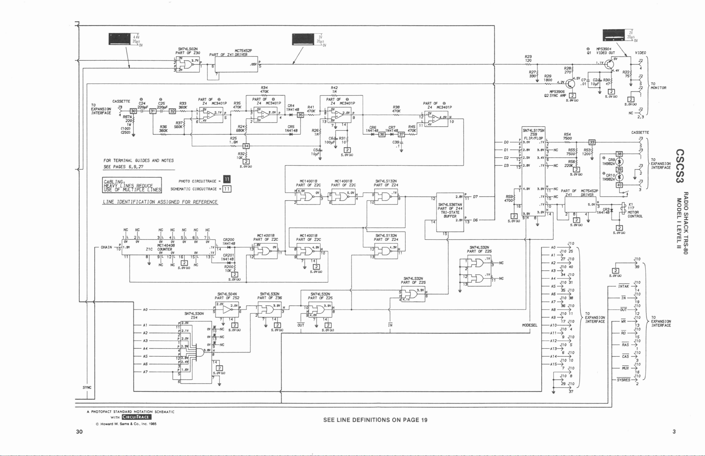
~
TO
EXPANSION
IHTERFACE
FOR
TERMINAL
SEE
PAGES
CABLING.
HEAVY
LINES
USEOFMULTIPLE
LINE
IDENTIFICATION
4V
20ILS
OV
GUIDES
6,9,27
REDUCE
e
AND
LINE
ASSIGNED
NOTES
sa£I1ATlC
SH74LS02N
PARTOF130
l .
PHOTO
CIRCUITRACE
FOR
~
CIRCUITRACE
REFERENCE
=
m
OJ]
R34
470K
~
CRS
IH<4H8
HCHOOIB
PARTOFZ2C
20llS
v
OV
R42
1M
HCHOO18
PART
OF
Z2C
SH74LSI32N
PART
OF
Z24
PART
Z4
OF
e
HC3401P
SH7<4LS367AH
PARTOFZ<4<4
TRI-STATE
SU'FER
"l.9V
..
~
5.r:NW
He-<
VIDEO
J2
J2
S
J2
2,3
TO
MONITOR
R23
120
R28
R27
330
R29
1800
DO
01
02
D3
07
p
D6
270
RS4
7500
7S00
4.5V
RSS
RS6
5.r:NW
C7
.01
2
SYNC
CMAIN
He
HC
He He
1.0
Al
1.2
A3
1.4
AS
1.6
1.7
He
He
SH7<4LS3ON
ZS4
He
.tN
HCHOOl8
CR200
L
IH4H8
<4
CR201
lH<4H8
R200
10K
2
5.r:NW
r:N
r:N
NC
,
r:N
He
H
8
PARTOFZ2C
l .
13
HCHOOl8
PART
OF
Z2C
SH7<4LSI32N
PART
OF
Z24
SH74lS32N
PART
OF
Z2S
SH7<4LS32N
PARTOFZ2S
He
HC
AO~
Jl02S
AI~
27
A2~
JIO
A3~
3<4
A<4~
JIO
AS~
3S
A6~
JIO
A7~
36
A8~
JIO
A9~
AIO~
JIO
AII~
A12~
JIO
A13~
AH~
JIO
AIS~
JIO
JIO
<40
JIO
31
JIO
38
JIO
II
17
JIO
<4
9
JIO
S
6
JIO
10
~O
~O
..
37
30
A
PHOTOPACT
@ Howard
STANDARD
WITH
li'·iYili'-f.'i.
W.
Sama & Co.•Inc.
NOTATION
SCHEMATIC
1985
SEE LINE DEFINITIONS ON PAGE 19
J

PART
no
a:
ItOOfSEl
--------'t-------M
CLOCK
--------'r---~
BIT
6
I--E:---
BIT
0
BIT
I
BIT
2
BIT
3 L83
BIT
4
BIT 5
BIT 6
BIT
7
BIT
BIT LBI
VCLR
~
BIT 6
-----------...,..,;,-j
20#s
LBO
L82
LB4
LBS
rN
.7'1 l
.7'1 P
5H?4LS04H
PART
a:
142
1110
~
5H?4LS04H
PART
a:
19
.:>o-&---NC
.:>o-F:-:;,-NC
::>O-F:-:;,-NC
FOR
TERti/NAL
SEE
PAGES
PHOTO
SCt£MA
11
CABLING.
HEAVY
USEOFMULTIPLE
LINE
IDENTIFICATION
GUIDES
6,9,71
CIRCUITRACE
C CI
RCU
ITRACE
LINES
REDUCE
HC
= m
=IT!]
LINE
~
AND
NOTES
ASSIGNED
~
5ms
FOR
REFERENCE
2V
2ms
OV
2V
OV
m;+----lf---------ll
fi.----+--------L2
h..---...L...t_------L4
m----....~:___-----~
5H?4LSIIH
PART
11'--
a:
166
--'
LB
1-E-+-A6
1-E-+-A7
I-+--i:-
'--+--i:-
AB
,1.9
~
2ms
----'-0
2V
L-~E---
e
e
1'tf74C04H
PARTOF157
He
1'tf74C04H
PARTa:157
~
~~sOV
BIT
VDRV
---?<t~
tflRV
---il-,J
LB
---------------,..,;...j
LATCH
--------------~
VCLR
--------,.
............
""';u-----,
..
He
R43
10K
VID
SYNC
LATCH
12
5H?..LS04H
PART
H
..
~.7'I
OF
5H?4LS02N
PART
a:
130
5H?4LSI32N
He
5N7..LSO..N
PART
OF
19
19
PARTOF124
@4NC
..
NC
31
A
fHOTOfACT
© Howard
STANDARD
WITH
lif·lailli-f.U'
W.
sams & Co..Inc.
NOTATION
SCHEMATIC
1985
SEE
LINE DEFINITIONS
ON
PAGE 19
32
33
RADIO SHACK
MODEL I LEVEL
TRS·BO
II
SMtS
__
C_O_M_P_U_"fJ_E_R_'FA_C_T._S_T1O
KEYBOARD, CPU BOARD
See Folder CSCS3
R_AM_D~_~_~_~~_~_
:V_~_~S_I~8_0
MONITOR
o
CJ)
o
CJ)
w
•
CD
SAFETY PRECAUTIONS
Disassembly
GridTrace Location Guide
Main Board 7
Video Board
Parts List
Monitor
Photos
Cabinet·Rear View
Chassis·Top View
Main Board 6,7,15
Video Board 13,14
Instructions
The listing of
constituteinany
HowardW.Sams & Co..
replocemen'
from information
monufocturers
any
coseQrecommendation.
port.
The
furnished
of
the
Howard
4300
available
Inc..asto,he
numbersofthese
particular
West
replocement
quality
to Howord W. Sams & Co.. Inc ..
typeof(&placement
8 thru
W.
62nd Street, P.O. Box 7092,
port
herein
warrontyorguaranty
and
suitabilityofsuch
ports
hove
See pages,4,5.
INDEX
Page
21
Placement Chart 3
Resistance Measurements 18
Schematic
14
12
21
20
Sams & CO., Inc.
does
been
compiled
by
port
listed.
Monitor
Notes
Terminal Guides 2
Safety Precautions 4,5
Servicing in the Field
Troubleshooting
Troubleshooting
not
ReproductionOfuse,
by
content.inany
respect
to
e
li85
4300
Printed
How...,
Wesl
in U.S. of Am
the
Aid
Indianapolis,
without
monner,isprohibited.Nopotent
the
useofthe
W.
62nd
Sir_I.
express
information
sam.
& Co
.•
In<:.
P.O.
80.7092.
...
ica. 85CC14942 DATE 2.85
Page
19
21
16,17
16
Indiana
46206 U.S.A.
permission.ofeditoriolorpictorial
contained
liabilityisassumed
herein.
Indianapolis. Indiana 46206 U.S.A.
2
with
::D
~»
2
0
0
0
m(f)
r"'"x
»
r"'"("')
m,..
<-4
~::D
_(f)
-cio
o

,...,
I - - - - - - - - - - - - - - -
I e 1I'S3904
I
Q2
HOISE
e
03
FILTER
R?
1500
306-B
SYNC
l.tvA
.033
100V
C33
ISO
RIO
R9
510
R28
2700 He He
13
R38
220/(
'~Ol
IA
• 5101
,...
C?O
+-~Io--"--------1~~---e~
•
1(17
10
P2
T
o
C
o
~--t'_{>-f
I Cl
II .
M
P2
.oo:n
500V
CR17
Tl031
CR18
031
1
39Ok'
I
I
I
I
R I
~~
J8
,...----~H
C34
R31
41
R6?
1~
7
R29
6800
2.211
1500
~
R30
R6.f
43
CS9
P
~
,...------'
I
I
I
I
I
I
I
R6S
S6<»(
R68
lOOk'
U
T
E
R
01
C10?
.001
SOOV
•
f1f'
nOI
.4
5
.5
C4B
E36
00
FBI
I
==
TO
J.K)
C28,CSO
C5?
TO
E30
J.K)
C61
,.,
•
I.S
ISOV
•
At
10
JB
J8
ps
He
~~~
C26
IJJF
JB
5
!
-----------,
PART
CR20
F046
C9
470JlF
Cl0
270JJF
OF
V
IDEO
ps
1
BOARD
5
".l\'lBl
__
ps
2~:
J8r1J8r
11.7V
c:n
IJJF
WA
A
SIGNAL.
ON
~
IIITH
VEFORtfSTAKEH
SIGNAL
VIDEO
5.0V
IIITH
A
APPlIED
BOARD
TO
CMQo/
APPlIEDTOPIN 1
TIE
10V
COf'f>OS
ITE VI
TOH£J1.fICTlONOFRl
POINT
OF
P2
DEO
SCHEMATIC
BAR
J.K)
Cl
PHOTO
CIRCUITRACE
CIRCUITRACE
=
=
III
UCO
l~
- - - - -
IOMS
C-4
.01
~flT
_of.
12r_---------------------\-------=----'
CR6
F031
R?4
47
r:::~:::::01-
IIIIIIIIII.II~S
12.IY
.'{I.QEJ)
J3Q.A!3.D
R73
390
11.IY
---
e 1f'S3904 e If'S3904
01
VIDeO
RS
180
100:47-
~S
»If>
5Y
12.IY
R13
6800
--------------
QS
R15
RH
:noo
3300
1I.8VlBl
~s
:"~
__
~!-4_
JB~4J8~
R75
330
~l9
9
CR8
031
500V
_
R46
lSOK
IS.
IV
f;fl
e
RSI
8200
CS6O)
666-1
~
I
lIE
.
7V
Ill.At«ER
e 303-1
09
.-Girv
r----------f-E------~----=----1E_-I22r_-----------...J
~s
R78
R?9
330 330
VIDeO
PS 8
JB
VERT
B
MPlJT
»If> I
R17
470
-----
R48
4700
-:
!!::::::!!!M]s
I 362--3
10 10
I
I
I
I
I
I
IlqlF
500V
f
~~::'''"'"
11
11
RS3
1
~
15V
~s
e K366-1
0101
Q2
VIDeO
l....-_-:---llf---+'
L..-.:lf--~
RSS
220
HORIZ
MPlJT
.2V
•
Clot
laGpF
TH881
C24
20bv
MPlJT
53
RS9
.f7OO
~~
RH
7SOO
3W
C1
Ok'.
III>
CS6OO.2lO
•
CI03
\ Cl01
"1
\'''1
CLIP
AI:DE.D
......
_'~·_H----,
FOR
II
10TH
FB101
I
=---~~+-----
.5
3."
"'---
...
~----TO
.5
II
,,"'----_-0---.,045
E27
__
7
s
2
3
5
He
---o88.3V
LV
E30
6
E36
POWER
IN
~
TO
CRTHVAHOOE
10.5n'TO11.5n'
TO
C107 C CR10?
INLVPOWER
01
Sl.f'PtY
TO
E30
IN
LV
POWER
SUPPLY
SUPPL
E18
5ms
Y
E BC
G
Q3
THRU
Q11,
Q12
BOTTOM
VIEW
Q9
E BC
BEVEL
Q101
BOTTOM
Q2
FRONT
VIEW
r·-----·--·····--·---·,
E B C
1
30
• • 3 6
5 • 4
2
G
Q1
THRU
BOTTOM
VIEW
Q5
P2
FRONT
VIEW
L •
VIDEO
__
• •
BOARD
1 2 3 4 5 6 7 8 9
2 7
10
4 5
TOP
101112
~~
J8
TOP
VIEW
FRONT
T
VIEW
101
VIEW
Z1
VIEW
__
••
8
~
A
fHOTOfACT
WITH
© Howard W. Sams & Co
2
STANOAao
NOTATION
"'i-i'i1"".'i_
.•
Inc. 1985
SCHEMATIC
RADIO SHACK
TERMINAL GUIDES MODEL I LEVEL II
TRS·SO

Zl
ISOLATION
Q3
o
VIDEO
BOARD
D
o
Q4
AMP
VIDEO
PREAMP
o
Q2
NOISE
FILTER
VIDEO
CONTRAST
."
..
J>
o
m
~
m
Z
-4
o
::I:
J>
:tJ
-4
Co)
BRIGHTNESS
CRI
~
Ql
cJ!I~EO
......
AMP
......
......
o
QS
VIDEO
AMP
......
......
......
SYNC
,...
............
......
Q2
VERT
[]
OUTPUT
II
131\31
09'S~:U
......
......
......
......
CR14
...
I
1300W
)4~VHS
......
......
I
I
I
I
CR9
'Q3J
SYNC
D
Q7
KINE
BLANKER
CR
'.
o
D"
Q4
VERT
QS
OSC
PREAMP
VERT
SIZE
OIOVij
CR12..
-"o.L
.....
R1
CR10
0
A +
Q6
CRB
VERT
iCR6
VERT
CR20
CR17
CR19
3
C~lB
b
...
~
*0
QB
VERT
OUTPUT
DRIVER
HORIZ
DRIVER
Qll
HORIZ
OSC
0
Q12
D 0
...
CR7
D
Q9
VERT
OUTPUT
HORIZ
HOLD
9-£5050
i
TOP
VIEW
tE]~
POWER
FACTORY
ADJUST
CR10l
*
AC
FUSE
lA
~
CR106
I
/
I I
\
-
Ql0l
HORIZ
--t-,
'"
/
OUTPUT
i
I
I I
I
1101
CR107
I
....
~
AC
HOLD
FUSE
SA
G

SAFETY PRECAUTIONS
NOTE: Before servicing
precautions
Before
checkofthe
The service
device
become
ing.
1.
Comply
locatedonor
monitor
2.
WARNING:
video
Any
jacks,
etc
ment
the user. Any
the
3.
display
supply.
with
ween the
very
cant
4.
5.
and the
returning
built
into
defective
display
design
limited
switches,
may
and
manufacturer's
manufacturerofresponsibility
property
HOT CHASSIS WARNING: The
monitors
is
solidly
may be serviced
if
the
power
nected
to the
an AC
low
reading is obtained, reverse the
recheck
chassis
Some
tiontothe
groundisNON-ISOLATED
line. The
sulating
altered in any way.
potential
the
polarityofthe
chassis
transformer
receiver and the AC
sonnel and test equipment.
Observe the original
tion
should
following
area, (c)
that
wiresorcomponentsdonot
parts.
Inspect
wiring
in all areas.
Components
should
be replaced.
"Product
any
entire
technician
with
chassisorpicture
to,
alter
damage resulting therefrom.
"Hot"
for
should
high
instrumenttothe
Video Display
the
instrument
or inadvertently defeated
all
caution
inside
Alterations
monitor
alterationsoradditions
circuit
grounding,
the safety
potentially
design
are
chassis
connectedtoone sideofthe AC line cord
without
plug is
grounded
voltmeter
chassis
AC reading
material
from
and a
a zeroorlow
have a secondary
main
two
ground
chassistoearth ground, regardless
AC supply. Service on
only
inserted in the
be takentoassure proper lead
areas:
(a)
voltage area,
for pinched, out·of-place,ordamaged
that
this
chassis, read and
Safety
Notice".
Monitor
must
be sure that no
by the
and safety related
the receiver cabinet and on the
tube.
of the
designorcircuitryofthis
should
not
be made.
modifications,
activeorpassive
characteristicsofthis
create a hazardous
alterationsoradditions
warranty and
connectedtoone sideofthe AC
equipmentinwhich
usinganisolation
insertedsothat
sideofthe AC supply. Check
to see of a
known
should
chassis
systems
which
Other
be performed
supply
correct
near sharp edges,
indicate
will
for
chassisofsome
earth ground. A zero
be obtained.Ifa
meter
reading.
ground
ground. The secondary
in respecttothe
are separated by in-
must
not
chassis
power
for
protectionofboth
lead dress. Extra precau·
(d)
video
evidence of overheating
follow
customer
should
manufacturer
such
auxiliary
further
personal
the
potential
be defeated
have an 85V RMS
withanisolation
line between the
input
touch
Copyright
a safety
be made.
protective
during
servic·
as,
but
speaker
circuitry,
situation
will
relieve the
injury
the
chassis
transformer
chassisiscon·
exists
signifi·
power
plug and
system
in addi·
these
types
dress
(b)
AC
wiring.
thermally
Corporation.
instru·
supply
these
has
notes
not
for
void
or
video
bet·
or
power
per-
in the
Insure
hot
Radio Shack, a DivisionofTandy
or
of
of
Used
6.
WARNING: The
integral
the same type
remove,
ner
so equipped
are handled. Keep
while
deflection
and is
remove
because
servicer.
7.
Protective shields are provided on
protectionofboth
customer. Protective
convenience
MISSING SHIELDS MUST BE REPLACED.
OPERATE THIS INSTRUMENT WITHOUT THE PRO·
TECTIVE SHIELDS IN POSITION AND PROPERLY
SECURED.
8.
When replacing a
tain
place,
fish
shields,
9.
VIDEO INPUT COLD CHECK
With
place a
strumentACswitch
one leadtothe jumperedACplug and
leadtoeach exposed coaxial
sistance
megohms. Any resistance value below
dicatesanabnormality
tion. Repeat the
position.
10.
LEAKAGE CURRENT HOT CHECK
(ON COMPLETE ASSEMBLED INSTRUMENT)
Plug the AC line cord
not use an
Leakage Current Tester
complies
(ANSI C101.1 "Leakage Current for
Underwriters
for
AC
cabinet (plugs, jacks, handle bracket, metal cabinet,
screwheads, metal overlays,
known
ticularly
the chassis. Any
0.5
test. ANY MEASUREMENTS NOT WITHIN THE LIMITS
OUTLINED ABOVE ARE INDICATIVE OF A POTENTIAL
SHOCK HAZARD AND CORRECTIVE ACTION MUST
BE
TO
with
permission.
implosion
installorhandle the
unless
shatterproof
should
handling. On
yoke is an integral partofthe
permanently
"permanently
of
possible
that
all the
such
as:
papers,
isolation
theACplug removed from the 120VAC source,
jumper
measured
isolation
with
current
with
switch
"off"
earth ground (waterpipe,
any exposed metal part having a return path to
milliamp.
TAKEN BEFORE RETURNING THE INSTRUMENT
THE CUSTOMER.
picture
number
mustbecorrectly
non-metallic
adjustment
across the
American National Standards
Laboratories (UL) 1410, (50.7). Measure
theACswitch
Reverse plug in the AC
tube
in thiS
monitor
protection.
be kept away
picture
"In·Line"
attached. Do
tube breakage and hazardtothe
the service
shields
chassis
protective
resistor
on. Using an ohmmeter,
should
test.
with
directly
transformer
from all exposed metal partsofthe
current
Replace
for
continued
picture
goggles
tube away from the body
attached"
in the cabinet, always be cer-
devices are
control
and
capacitor
two
which
the AC
orametering
measured
tube
are worn. People
while
type
picture
yoke from CRT
this
technician
removed
re·installed and ANY
knobs,
compartment
networks,
plug prongs. Turn the in·
connector.
not be less than
requires
switch
into
a 120 VAC
for
this
Appliances")
"on"
and repeat
control
shafts,
conduit,
must
outlet
employs
withatube
safety. Do
in any man·
picture
tubes, the
picture
not
attempt
chassis
touch
for
and the
for
servicing
DO
put
back in
insulating
covers/~
etc.
connect
the
The
this
range in·
corrective
in the OFF
outlet
check). Use a
system
Institute
with
etc.)toa
etc); par-
not exceed
and repeat
not
not
tubes
tube
the
NOT
other
ac-
(do
which
and
the
of
to
re-
20
4

SAFETY PRECAUTIONS (Continued)
DEVICE
UNDER
TEST
2·WIRE CORD
PLUG AS REQUIRED) GROUND
11.
X·RADIATION
The primary
state
video
picture
x-radiation
tection,
as the original. The
picture
and
must
High
voltage
required
high
voltage. Where used, x-radiation
cuits
(may
(READING SHOULD
NOT BE ABOVE
a.5mA)
ALL
TEST
EXPOSED METAL
SURFACES
ALSO TEST WITH
PLUG REVERSED
(USING ADAPTER EARTH
AC LEAKAGE TEST
AND
HIGH VOLTAGE LIMITS
sourceofpotential
display
monitorsisthe
tube
is
specially
emissions.
the replacement
tubes
have an x-radiation
be properly in place.
must
that
involves B +, horizontal
also
For
tube
shields
be checked each
be referredtoas horizontal
\-
x-radiation in
constructed
continued
must
and
mounting
protection
©
-\0
_.~
picture
x-radiation pro-
be the same type
time
Protection
Copyright
LEAKAGE
CURRENT
TESTER
solid
tube. The
to
prohibit
hardware
any service is
deflection
Corporation.
for
function
Cir-
disable
Radio Shack, a DivisionofTandy
or
or
hold-down)
time
fertothe Technician x-radiation
Chassis
strument
chassis
cuits
High voltage is maintained
the use
and
voltage exceeds
nent
take necessary
12. PRODUCT SAFETY NOTICE
Many
have special safety-related
characteristics
spection
necessarily be
ponents
placement
characteristics
plements
such
schematics
its
Supplements
replacement
characteristics
shown
plements
hazards.
Used
with
permission.
must
the x-radiation
Schematic
Labels
and, where used, x-radiation
specifications.
of
close
adjustments
specified
electrical
nor
can the
rated
parts
and
Bulletins.
features are
and by # on the Parts
which
in the Parts
and
Bulletins,
be checked
Protection
in the Basic Service Data and In·
for
specific
tolerance safety related
in the
specified
on the
corrective
and mechanical
are
often
obtainedbyusing
for
higher
which
are
identifiedinthis
and
Bulletins.
does
as the recommended replacement part
for
proper
operation
Circuitisserviced.
warning
high
voltage
within
high
voltage
limits,
check
chassis
identified
Listinthis
schematic
action.
parts
characteristics.
not
evident from visual in-
protection
voltage, wattage, etc.
have these special safety
Electrical
not
may create shock, fire,orother
components
by
Listinthis
The use of a
have
note
limits
of each
Protection
specified
afforded by
replacement
Data and
shading on the
the
Data and
limits
components
circuit.Ifhigh
each compo-
diagram and
in television
its
having
Data and
substitute
same safety
its
each
Re-
on the
Cir-
sets
These
them
com·
Re-
Sup-
Sup-
by
o
en
o
en
(,,)
•
tD
~>
0
cO
men
I:I:
->
10
m",
<
m-i
I::tI
_en
-eo
::tI
52
o
5
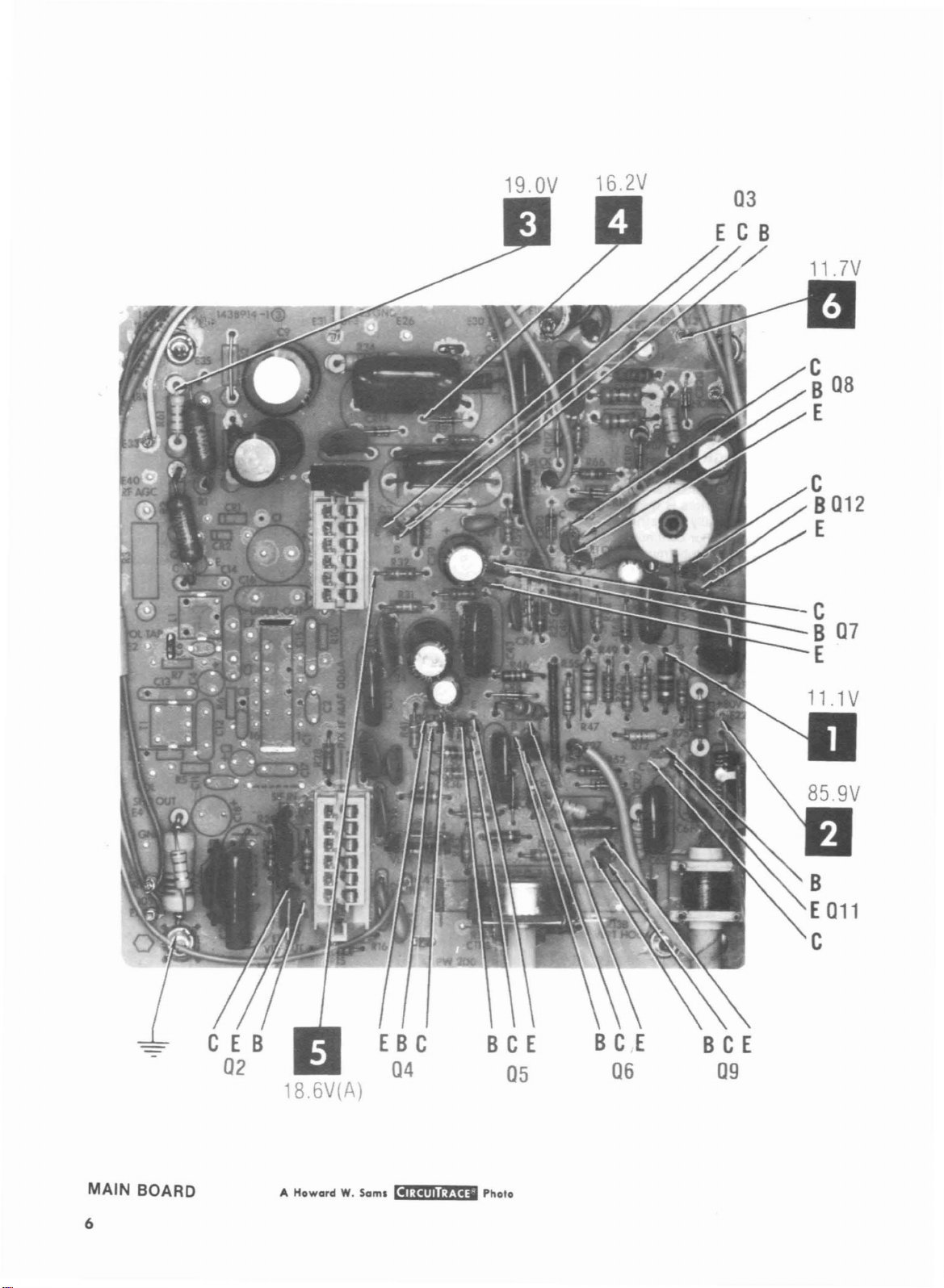
19.QV
16.2V
MAIN
6
BOARD
18.6V(A)
A HowardW.Saml
(li1·ii.iii".,3' Photo

MAIN
BOARD GridTrace LOCATION GUIDE
C9
Cl0
C22
C23
C24
C25
C26
C27
C28
C29
C33
B-3
0-3
K-5
L-5
K-3
F-7
1-11
6-10
D-6
F-8
H-5
1 2
C34
C35
C38
C39
C40
C41
C42
C43
C44
C45
C48
3
G-5
1-5
1-7
E-6
G-6
J-,9
H-6
G-7
B-5
F-8
B-7
4
C49
C50
C51
C56
C57
C59
C60
C61
C62
C63
C64
5
E-7
0-4
0-5
J-6
1-5
C-7
0-8
B-7
B-8
F-9
F-l0
6
7
C65
C66
C68
C69
C70
m4
CR6
m7
CR8
m9
ml0
8
9
J-l0
1-10
F-l1
E-l0
0-11
F-8
J-7
1-9
H-7
C-6
E-8
m12
m13
CR14
m17
m18
m19
m20
FBI
FB4
FB5
FB6
FB7
L2
10
A
B B
C
0
E E
F
G
H
J
K
L
1 2
3
4
5
6
A
HowordW.Soms
7
@jlieJI;tJiW
8
9
10
Photo
B-7
0-6
C-5
C-8
0-9
0-9
C-l0
B-7
E-l0
F-l0
0-9
C-9
K-2
11
A
C
0
F
G
H
J
K
L
11
MAIN BOARD
L3
L4
L5
Q2
Q3
Q4
Q5
Q6
Q7
Q8
Q9
Qll
Q12
Rl
R2
R9
RUB
R14
R15
R16
R18
R19
R20
R23
R24
R25
R28
R29
R30
R31
R32
R34
R35
R36
R37
R38
R39
R40
R41
R42
R43
R44
R45
R46
R47
R48
R49
R50
R51
R52
R53
R54
R55
R59
R60
R61
R64
R65
R66
R67
R68
R69
R70
R71
R72
R73
R74
R75
R76
R77
R78
R79
R80
R81
J-3
K-l1
E-l0
K-3
E-5
H-6
H-6
1-8
F-7
E-8
K-9
1-10
F-l0
C-2
E-2
C-2
K-7
K-l
L-4
L-4
K-4
K-2
K-3
H-l0
B-9
F-8
1-4
G-5
E-6
F-5
F-5
B-5
J-7
1-6
J-8
J-6
1-8
G-6
H-6
J-7
J-6
J-6
H-7
G-7
H-9
F-9
H-9
1-6
F-6
1-9
J-8
J-9
H-8
E-7
0-7
C-2
C-6
C-8
0-9
C-8
G-9
F-l0
H-9
H-l0
H-9
H-l0
J-ll
H-l0
F-ll
0-10
C-9
C-9
C-l0
K-2
(")
en
(")
en
~
•
CD
:xJ
3:>
2
0
0
0
mC/)
'::I:
->
,n
m"
<-4
~:xJ
_C/)
-0,
0
7

00
PARTS LIST AND DESCRIPTION
When ordering parts, state Model, Part Number, and Description
SEMICONDUCTORS (Select replacement for best results)
ITEM
No.
ffi4
CR6
ffi7
CR8,9
CRIO
CR12
ffi13,14
CR17
ffi18
ffi19
ffi20
ffil0l
TYPE
No.
F084
F031
F060
031
F031
A-231
F084
TI031
031
A24015
F046
RC185-6
139706
119597
119597
119597
119597
138173
139706
119597
119597
119597
139706
141489
MFGR.
PART No.
GENERAL
ELECTRIC NTE ECG
PART No.
GE-300
GE
-300
GE-300
GE-300
GE-300
GE-511
GE-300
GE
-300
GE-300
GE-300
GE-300
GE-510 NTE125
NEW·TONE
PART No.
NTEl77
NTE
177
NTE177 ECGl77
NTE
177
NTEI77
NTE552
NTEI77
NTE
177 ECGI77
NTEI77
NTEI77 ECGI77
NTE177 ECG177
PHILIPS
PART No.
ECG177
ECGI77
ECGI77
ECGI77
ECG552
ECG177
ECG177
ECG125
REPLACEMENT DATA
RCA
PART No.
SKOO91/177
SK9091/177
SKOO91/177
SK9091/177
SKOO91
1177
SK3130
SKOO91/177
SK9091/177
SKOO91/177
SK9091/177
SKOO91
1177
SK5010/117A
WORKMAN
PART No.
WEP10621177
WEP1062/177
WEP10621177
WEP1062/177
WEP10621177
WEPl72/506
WEP1062/177
WEP1062/177
WEP1062/177
WEPI
062/
WEPI
WEP170/125
177
06211 7 7
ZENITH
PART No.
103-131
103-131
103-131
103-131
103-131
103-287
103-131
103-131
103-131
103-131
103-131
212-Z9000
ffil06
CR107 M132
CRl08
02
03
04,5
06
07
08
09
011
012
0101
T14881
A8293O-6(1)
362-3
7362-3
306-8
7306-1
112-8
1112-8
318-2
7318-2
666-1
3666-1
349-2
7349-2
303-1
7303-1
6143H827
3614-3
306-1
7303-1
M366-1
7366-1
(3)
140972
138173
(2
)
141295
141330
132830
139268
137155
141008
137340
137875
137340
140976
GE-511 NTE558
GE-511 NTE552
GE-27
GE-27
GE-123AP NTE123AP
GE-123AP
GE-82 NTE159
GE-82 NTE159
GE-220
GE-220
GE-82 NTE159
GE-82
GE-123AP
GE-123AP
GE-82 NTE159 ECG159
GE-82
GE-123AP
GE-123AP NTE123AP
GE-82 NTE159
GE-82 NTE159
GE-38
GE-38 NTE165
NTE171
NTE171
NTE123AP
NTE194
NTE
194
NTE
159
NTE123AP ECG123AP
NTE123AP
NTE
159
NTE123AP
NTE165
ECG558
ECG552
ECG171
ECG171
ECG123AP
ECG123AP
ECG159
ECG159
ECG194
ECGI94
ECG159
ECG159
ECG123AP
ECG159
ECG123AP
ECG123AP
ECG159
ECG159
ECG165
ECG165
SKOO00/552
5K3130
5K3201/171
SK3201/171
5K3854/123AP
5K3854/123AP
5K3466/159
5K3466/159
SK3479
5K3479
5K3466/159
SK3466/159
5K3854/123AP
5K3854/123AP
5K3466/159
SK3466/159
5K3854/123AP
SK3854/123AP
5K3466/159
5K3466/159
5K3115/165
5K3115/165
WEPI72/506
WEPI72/506
WEP702/171
WEP702/171
WEP736/1 23A
WEP736/123A
WEP621159
WEP62/159
WEP64/194
WEP64/194
WEP62/159
WEP62/159
WEP736/1 23A
WEP736/123A
WEP621159
WEP621159
WEP736/123A
WEP
736/1 23A
WEP621159
WEP62/159
WEP74OB/165
WEP740B/165
103-287
103-287
121-822
121-822
121-Z9000A
121-Z9000A
121-Z9003
121-Z9003
121-881
121-881
121-ZOO03
121-Z9003
121-ZOO00A
121-Z9000A
121-ZOO03
121-Z9003
121-Z9000A
121-Z9000A
121-ZOO03
121-Z9003
121-1029
121-1029

PARTS LIST AND DESCRIPTION (Continued)
When
ordering parts, state
Model,
Part Number, and Description
SEMICONDUCTORS (Select replacement for best results) (cant)
CRI
01
03
Q4
05
Zl
ITEM
No.
thru
Numberonun
(1)
(2)
Part
Maybepart
(3)
TYPE
No.
VIOCO
BOARD
1
N5242B
lN4742
MPS3904
2N3904
MPS3906
2N3906
MPS3904
2N3904
6N135
/-P5082-4351
5082-4350
of
It.
Horlz Output
of
Ql01
PART
4800037
4822001
4822003
4822001
3106001
Transformer
In
some
versIons.
MFGR.
No.
Tl01
Part
GENERAL
ELECTRIC
PART
GEZD-12
GEZD-12
GE-123AP
GE-123AP
GE-82
GE-82
GE-123AP
GE-123AP
No.
140995.
No.
NEW·TONE
NTE
PART
No.
NTE5021A
NTE142A
NTE123AP
NTE123AP
NTE159
NTE159
NTE123AP
NTE123AP
REPLACEMENT
PHILIPS
ECG
PART
No.
ECG5021
ECG142A
ECG123AP
ECG123AP
ECG159
ECG159
ECG123AP
ECG123AP
A
DATA
RCA
PART
No.
SK12A15021A
SK12V/142A
SK3854/123AP
SK3854/123AP
SK3466/159
SK3466/159
SK3854/123AP
SK3854/123AP
WORKMAN
PART
No.
WEP1423/5021
WEP1112/142
WEP736/123A
WEP736/123A
WEP621159
WEP62/159
WEP736/1
WEP736/123A
23A
ZENITH
PART
No.
103-279-21
103-Z9003
121-Z9000A
121-Z9000A
121-Z9003
121-Z9003
121-Z9000A
121-Z9000A
WIRING DATA
High
Voltage
Shielded
General-use
-0
Lead
Hook-up Wire
Unshielded Hook-up Wire
••••••••••••••••••••••••
••••••••••••••••••••
••.•••
Use'BELDEN
Use
BELDEN
Use
BELDEN
No.
8869 (17
No.
8401
8208 (Two-Conductor)
No.
8529
8522
09'S~:U
KV)
or
8421
(Solid)
(Stranded)
II
131\31 I
(Single-Conductor)
Available
Available
1300W
)f~'fHS
OIO'fl:j
In13Colors
In13Colors
S-ESOSO

PARTS LIST AND DESCRIPTION (Continued)
When ordering parts, state Model, Part Number, and Description
ELECTROLYTIC CAPACITORS
#
ITEM
No.
C113A
Items
#
For
B
SAFETY
RATING
200
250
numbers
CAPACITORS
ITEM
No.
Cl01
#
Cl02
#
Cl03
#
.18
36
.1
use
RATING
200V
N750
200V
175V
175V
not
only
10%
5%
10%
lIsted
equIvalent
PAIIT
140969
are
normally
139318
142023
242290
MFGIl.
No.
replacement
MFGR.
PART
No.
avaIlable
part.
ITEM
No.
at
local
ITEM
No.
Cl05
#
Cl08
I
ClIO
I
RATING
dIstrIbutors.
.0015 1.2KV
180
125VAC
.1
RATING
MFGIl.
PAIIT
141496
143029
133343
No.
MFGR.
PART
No.
Items
For
numbers
SAFETY
#
use
not
only
listed
equIvalent
CONTROLS (All wattages
#
#
#
ITEM
NO.
Rl38
R44
Rl02
Rl03
#
For
(1)
SAFETY
Number on
FUNCTION
Vert
Hold
Vert
SIze
Contrast
BrIghtness
use
unIt.
only
equIvalent
are
normally
1/2
RESISTANCE
200<
500<
500
200<
replacement
avaIlable
part.
at
local
distrIbutors.
watt, or less, unless listed)
MFGR.
PART
NO.
141022
replacement
1473351-2(1
138145
1473359-27<1)
140980
1472242-43<1 )
140711
part.
)
NOTES
10

PARTS LIST
When ordering parts,
AND
state
DESCRIPTION
Model, Part Number, and
(Continued)
Description
RESISTORS (Power
ITEM
No.
Rl 75
#
R2
I
R9
#
R14
R23 470
#
R24
#
R34
I
R40
R47
R49
R52
R54
#
R61
#
R77
#
R80
#
Rl08
#
Rl09
#
R112
#
Rl14
#
R118
#
R121
#
R12 200
#
For
SAFETY
(1)
Number
5%2WMetal
755%2W
10
5%
75005%3W
10K
lW
56005%2W
5%
4.7
5%
56
5%
W(
2%
12K
2%
12K5%112W
1202%
1502%
5.6
5%
3.3
5%
10
5%
4.7
5%
6800
68005%
22
5%
130
5%
2200
2000 1
1305%7W
VI~O
10%5WWW
use
only
on
unIt.
5%
5%
and
Metal
1/2W
Metal
Metal
1/2W
Metal
1/2W
Metal
1/2W
Carbon
1/4W Carbon
1/2W
Carbon
Carbon
1/4W
Carbon
1/4W Carbon
1/2W
Carbon
1/2W
Carbon
1/2W
Metal
1/2W
Carbon
1/2W
Carbon
1/2W
WW
7ti
WW
lOW
WW
equIvalent
Carbon
WW
lOW
(Jti
BOARD
Special)
RATING
OxIde
OxIde
OxIde
OxIde
OxIde
OxIde
FIlm
FIlm
FIlm
FIlm
FIlm
FIlm
FIlm
FIlm
OxIde
FIlm
FIlm
FIlm
replacement
part.
MFGR.
PART No.
832075
832075
830010
832256
830147
140986
830056
132855
143031
139324
830010
140986
993151-249
993151-249
143030
94
5312-1
209895
945311-128<l
249398
945312-157<l
209895
945311-128(1
4717002
09<l
REPLACEMENT DATA
NEW·TONE
PART No.
2W075
2W075
HW010
lW310
2W256
HW147
HW4D7
HW056
QW310
HW312
HW312
QW112
QW115
HW5D6
HW3D3
HW010
HW4D7
HW268
HW268
10W022
)
)
IOW222
)
)
WORKMAN
PART No.
22-2224
22-3120
22-4114
22-2237
22-2040
22-2066
22-2253
22-2122
22-2230
22-2231
22-2042
22-2036
22-2048
22-2040
22-2116
22-2116
24-4093
24-3070
:xJ
3:»
2
0
cO
mC/)
r-:J:
-»
r-O
m"
<
....
~:xJ
C/)
-eo
o
COILS (RF·IF)
MFGR.
PART
L2
ITEM
No.
FUNOION
RF
Choke 109946
COILS & TRANSFORMERS (Sweep
,
DYl
L4
L5
,
nOl
#
(1)Incl
For
ITEM
No.
SAFETY
udes
Yoke
90°
Horlz
Hor1z
Hor
use
CR108.
HorIz4.
Vert
Hold
DrIver
I z
Output
only
FUNOION
6Irti
51mH
equIvalent
replacement
No.
Circuits)
143045
141017
141021
(1)
140995(1)
MFGR.
PART
part.
No.
L3
ITEM
No.
FUNOION
Peak I
n9
REPLACEMENT
OTHER
IDENTIFICA
1463734-504
1463734-503
1465914-503
1465914-501
liON
DATA
MFGR.
PART
130131
THORDARSON
PART
No.
No.
11

PARTS LIST AND DESCRIPTION (Continued)
When ordering parts, state Model, Part Number, and Description
FUSE DEVICES
ITEM
NO.
,
F10l
,
Fl02
#
For
SAFETY
DESCRIPTION
1AII250V
Fast-ActIng
5AII250V
Fast-ActIng
Plgta
II
use
only
equIvalent
DEVICE
426973
99328
replacement
part.
MISCELLANEOUS
#
I
#
#
ITEM
No.
OSIOI
FBI
FB4
FB5
FB6
FB7
FB10l
L10l
P10l
SIOI
VIOl
PART
Neon
Lamp
FerrIte
FerrIte
FerrIte
FerrIte
FerrIte
FerrIte
F
errIte
Power Cord
SwItch
CRT
CRT
Bracket
CushIon
P.C.
Board
P.C.
Board
Socket
NAME
Bead
Bead
Bead
Bead
Bead
Bead
Bead
MFGR.
PART
No.
122608 NE-2H
119971
128456
128456
128456
128456
138013
143038
142453
142639
12VBYP4
12VBNP4
141006
132272
143035
1700065
143036
Main
MFGR.
PART NO.
AC,PoJarI zed
Power
AC
Power
CRT
VIdeo
CRT
Cord
MountIng
NOTES
HOLDER
NOTES
#
For
SAFETY
use
only
equIvalent
replacement
part.
CABINET & CABINET PARTS (When ordering specify model, chassis & color)
PART
CabI
net
CabInet
Button-Power
#
For
SAFETY
12
ITEM
Back 141856
Front
Mask 142312
use
only
equIvalent
140783
replacement
No.
part.
I
Knob-BrIghtness,
#
Knob-Hor1z
ITEM
Hold
Contrast
PART
136347
124313
No.

A HowordW.Sama
[iji.ijMihD
Photo
VIDEO BOARD
13

- <
~
-
c
m
0
OJ
0
»
::J:J
C
}-
I
0
~
a.
:E
0
'"
3
'"
. 1 ..
A
'ElJJl!JUULJ;
B
l--:J
C .
[
~
••
]~~~61"~~·[j]IIII[lI!E!j~
3
--~J
5 6 7 8 9
Ifiiiii]Onn
..
; .
(~.J.;~?",.~
."
~,4
,,~~_,~,
-.
~~.
••
'f'
.r.-:
I
_10
lliJnn~1
-
•...
,.
..
j~
:
....
bJ~L'
. . C
' " .
12
13
A
B
DD~lIl1li1lilllllililllt:JDD
1~111J1I~~II~.flj-[]~
,
0
[E]1I1I1I[jDIIEJ[]~~_IJ~
G
r41r-1
H ]tt:lLJ1
••
______
rIi1nll~fjr-;ltn~rr-]
Ii8II;
__
l
.j~~'<'1
G
H
VIDEO BOARD
GrldTrace
LOCATION GUIDE
B-3
B-9
E-3
0-5
E-8
E-l1
1-8
C-ll
E-9
F-2
F-40
H-7
H-l1
C-5
C-9
C-9
B-5
0-9
E-2
E-2
E-4
E-5
F-l0
1-3
H-8
G-8
G-9
H-l0
H-12
F-ll
E-7
I
Cl
C2
C3
C4
C5
C6
C7
CRI
Ql
Q2
Q3
Q4
Q5
Rl
R2
R4
R5
R6
R7
;\8
R9
RIO
Rl1
R12
R13
R14
R15
R16
R17
R18
ZI
J
1I 2
J
43
5
6
7
8
9
10
I
11I12r13

::D
~>
2
0
0°
mC/)
r-:I:
->
r-o
m",
<-4
~::D
_C/)
o
-=
A Howard W.
Sam.
[tIl
A""''''3i
i
Photo
MAIN BOARD
15
TROUBLESHOOTING AID
Note: Waveforms taken
Controls
PICTURE
NO PIC, NO RASTER: Check for AC power supply and sources generated from Horizontal
"Troubleshooting"
NO PIC, HAS RASTER: Referto"Troubleshooting"
LOWOREXCESSIVE BRIGHTNESS: Check Video and Luminance
SWEEP
NO RASTER: Check HV rectifier, Part
NO VERT DEFLECTION: Referto"Troubleshooting"
POOR
VERT LINORFOLDOVER: Referto"Troubleshooting"
POOR
HORIZ LINORFOLDOVER: Referto"Troubleshooting"
NARROW PICTURE: Referto"Troubleshooting"
VERT OFF FREOUENCY: Referto"Troubleshooting"
HORIZ OFF FREOUENCY: Referto"Troubleshooting"
SYNC
adjusted for normal operation.
with
trigged scope, Bar-Sweep generator. Schematic voltages measured
Power Supply and Horizontal
of
Horizontal
circuits.
Video
Output
Vertical
Horizontal
Vertical
Horizontal
circuit.
circuits.
Trnasformer(T101). Referto"Troubleshooting"
circuit.
Vertical
Horizontal
circuit.
circuit.
circuit.
Referto"Troubleshooting"
circuit.
circuit.
Output
with
digital
Transformer
Video
Horizontal
meter,nosignal.
(T101).
Refer
circuit.
circuit.
to
to
NO VERT/HORIZ SYNC: Refer
Note: Make sure
lose raster,orsync, or both, accordingtowhichever signal is
that
the problem is in the
"Troubleshooting"
Monitor
and
TROUBLESHOOTING
POWER SUPPLY
Check AC Fuses
CR101, and Capacitor C110.
good, check for 133V at cathode of Diode CR101.
missing,
for
Check
if
(T101),
the voltages developed
19.0V at
of
ResistorsR9and
any
sociated
HORIZONTAL
Check the Horizontal
check the waveform at base
sistor
forms and
Check waveform at base of Transistor 0101 and
check the voltages, waveforms and
with
sistor
junctionofResistorsR9and
Capacitor
of
the voltages are incorrect, check
(011). If waveform is missing, check voltages, wave-
Horizontal Driver
012
(F101
and F102) andifopen, check Diode
If
Fuses
F101
and F102 are
If
133V is
check Resistor R112 and Power
88.3V at pin 2ofHorizontal
missing,
with
check Resistors
from
C44
and
Electrolytic
R32,
11.7V at pin 5ofTransformer
that
voltage.
Output
components
are good, check Diodes CR106 and CR108 and
associated
Transistor
R121
Transformer T101. Check
C39, 18.6V at
Transistor
of
Horizontal
components
(012). If readings at Tran-
Switch
Output
Transformer
and
R114.
R61,
16.2V at
components
(0101). If good,
Oscillator
with
Transistor
(S101).
Check
junction
junction
n01.
if
missing,
associated
Sync
notinthe
for
of
If
as-
Tran-
011.
circuit.
Computer. If the
missing
Horizontal
developed by Transformer
down
the horizontal circuit.
For horizontal linearity or foldover problems, check
Capacitors C108, C105, C101, C102 and C103 and
Deflection
VERTICAL
Inject a vertical signal at base
sistor
(04) and check
no vertical
the baseofVertical Driver Transistor (06). If vertical deflection
returns, check voltages and
with
Transistor04and Preamp
deflection
Blanker
09),
For
Diodes CR6 thru
Capacitors
ments
and bias
Transistor
Deflection
poor
Chart"
Monochrome
from the
Output
Yoke (DY1).
deflection
does
vertical linearity or foldover problems, check
C41
circuitry
Computer
Transformer (T101). Check the voltages
for
not
(07), Vertical
Yoke (DY1) and associated components.
CR1O,
and C45. Refertothe"
and check
resistances.
Adapter fails,
to Monitor.
n01,
which
may be loading
of
vertical
is noted,
return, check
Electrolytics
for
Vertical
deflection
inject
the
vertical signal
components
Transistor
Transistor
Output
Transistors
C39,
C40
Resistance Measure-
possible changes in feedback
the
Oscillator
Monitor
on the CRT. If
05.Ifvertical
and C42 and
will
the
Tran-
associated
06,
Kine
(08
and
to
16
TROUBLESHOOTING (Continued)
VIDEO
Inject
a video signaltobaseofVideo Amp
on the Video Board. Check waveform at base
put
Transistor
ing,
check
with
ated
8 of
IsolationIC(Z1)
present at base
sistor
02,
cathodeofthe CRT.
No
video
Check
the
Computer
Video Board by
sistor
(02), Video Preamp
associated
(02) on the Main Board. If waveformismiss-
voltages, waveforms and
Video
Amp
Transistors
on the Video Board.Ifthe waveform is
of
Transistor02on Main Board,
the CRT and
with
for
Computer
5.0V at pin 2 of IC Z1.
andifmissing,
substitutionorcheck
components
components
on the Video Board.
connectedtoConnector
check
Transistor
components
(01 and04and
associated
This
voltage is
Computer. Check the
Noise
(03) and ICZ1and
Transistor
of
Video Out-
associ-
pins
check
with
supplied
Filter
(04)
5 thru
Tran-
the
P2.
by
Tran-
SYNC
No
verticalorhorizontal sync. Check voltages and wave-
forms
at base and
(03).
No
vertical sync.
Oscillator
associated
No
CR18.
circuitry.
(04).
components.
horizontal sync. Check waveformsatDiodes CR17 and
Check
collector
Check
Check
the Horizontal Hold Coil (L4) and
of Sync Separator
waveformatbaseofVertical
Vertical Hold
Control
(R13B) and
associated
Transistor
::0
3:>
O~
cO
mCJ)
r~
->
ro
m",
<0004
pJ::o
_CJ)
-!Xl
o
17

....
Q)
ITEM
VIOl
VIDEOBeARD
PIN
INF
RESISTANCE MEASUREMENTS
MEASUREMENTS TAKEN WITH LOW POWER OHMS METER
PIN
PIN
5
PIN
INF
6
PIN
7
PIN
8
PIN
0
1
PIN
2
PIN
3
PIN
4
730K
FIL
FIL
INF
PIN
9
10
PIN
11
PIN
12
PIN
13
14
Zl
ITEM
Q2
Q3
Q4
Q5
Q6
Q7
(1)
Reading
INF INF
E B
200
0
6000
55()(
8285
8285
may
516
33()(
870K
1M
114K
0
vary according to the condition of the
500K
C
1.
5M
3959
1M
1141<
355K
INF
INF
0
ITEM
Q8
Q9
Qll
Q12
Q101
electrolytic
47K
E
1.6M
1.6M
57
INF
0 6
in the
12K
B C
325K
316K
INF
3021
circuit.
630
INF
5
5501<
7
INF
(1)
ITEM
VIDEO
BC
Q1
Q2
Q3
Q4
Q5
E B C
II,RD
182
INF
800K(1)
1327
469
47K
INF
INF
6170
1326
2109
INF
580K
0
2290

SCHEMATIC NOTES
#
For
SAFETY
parts list.
Circuitry
Circuitry
9
See parts
? Ground
Chassis
Waveforms and voltages are taken from ground, unless
noted otherwise.
Item numbers in rectangles appear in the alignment/ad·
justment
Supply voltages maintained as shown at input.
Voltages measured
Controls
Terminal
Capacitors are
Electrolytic
noted.
Resistors are
Value in ( ) used in some versions.
Measurements
use
only equivalent replacement part, see
not used in some versions
used in some versions
list
instructions.
with
digital
meter, no signal.
adjusted for normal operation.
identification
50
capacitors are50volts or less, 20% unless
V2W
may
notbefound on unit.
voltsorless,5%unless noted.
or less, 5% unless noted.
with
switching
as shown, unless noted.
19
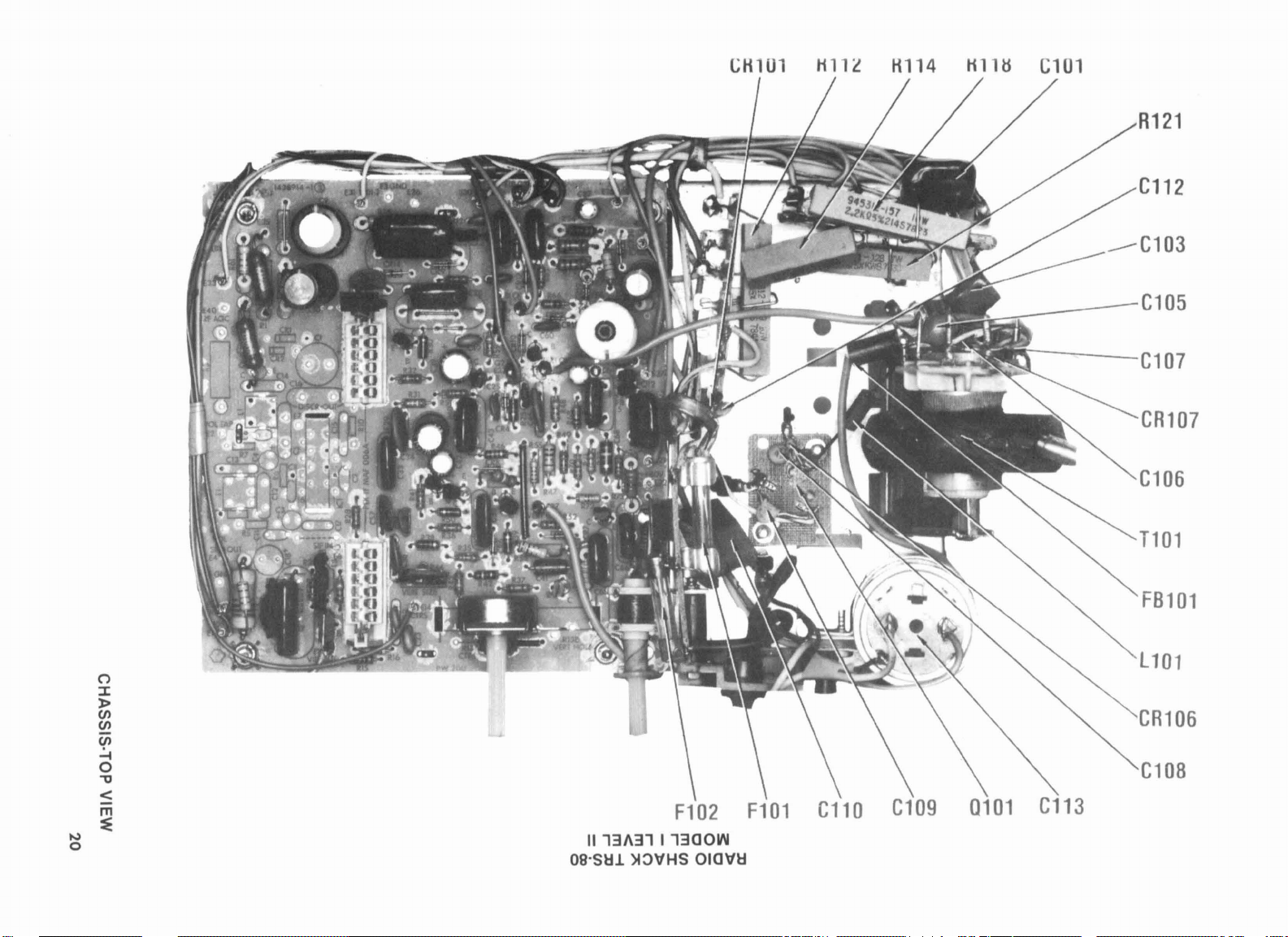
CH1Ul
Hlll
Hl14
H1HS
_----Cl05
Cl01
R121
Cl12
Cl07
CR107
Cl06
T101
FB101
l101
o
~
l>
C/)
C/)
C/)
~
o
."
<
m
:E
l',)
o
II
131\31
09·S~U
Fl02
I 13QOW
:>40VHS
OIQV~
Fl01
Cll0
ClOg
0101
C113
CR106
C10B
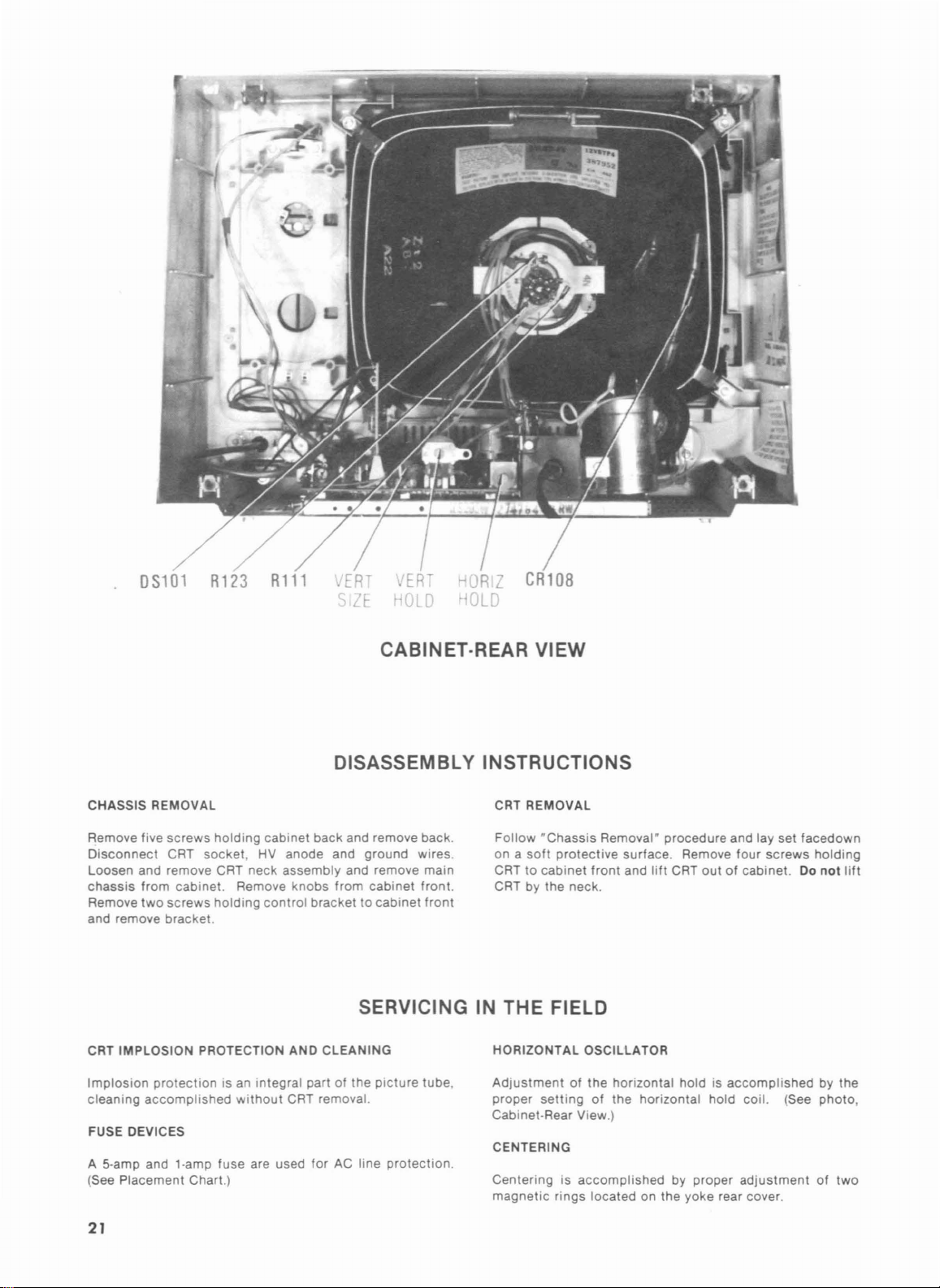
DS101
R123
CABINET·REAR VIEW
DISASSEMBLY INSTRUCTIONS
CHASSIS REMOVAL
screws
Remove five
Disconnect
Loosen and remove CRT neck
chassis
Remove
and remove bracket.
from cabinet. Remove
two
holding
CRT socket, HV anode and
screws
holding
cabinet back and remove back.
assembly
knobs
control
brackettocabinet
ground
and remove main
from
cabinet
SERVICING IN THE FIELD
CRT IMPLOSION PROTECTION AND CLEANING
Implosion
cleaning
FUSE DEVICES
A 5-amp and 1-amp fuse are used for
(See Placement Chart.)
21
protection
accomplished
is an integral partofthe
without
CRT removal.
AC
picture
line
wires.
front.
front
tube,
protection.
CRT REMOVAL
Follow
"Chassis
soft
on a
CRT to cabinet
CRT by the neck.
HORIZONTAL OSCILLATOR
Adjustmentofthe
proper
Cabinet·Rear View.)
CENTERING
Centeringisaccomplished
magnetic
setting
Removal" procedure and lay set facedown
protective
rings
surface. Remove four
front
and
lift
horizontal
of the horizontal hold coil. (See photo,
located on the yoke rear cover.
CRT
outofcabinet. Do
holdisaccomplished
by proper
screws
adjustmentoftwo
holding
not
lift
by the

~
~.
o
~
cn-
a::..J
~w
~>
O~
<-
J:..J
cnw
0
0
-0
o~
<
a::
<
C")
en
(J
en
(J
....
•
~
COMPUTCRCACTsn.
'_
IL_ln_/""\__,_
'
KEYBOARD, CPU BOARD
See Folder CSCS3
RADIO SHACK TRS·80
Miii,,;,0~D_E
..L..1.,LE..V.E;,;L;,.;I..I _
EXPANSION INTERFACE
(")
en
(")
en
w
•
»
PRELIMINARY SERVICE CHECKS
ENCLOSED
INDEX
Page
Disassembly
GridTrace Location Guide
Expansion Interface Board 8,13
IC Pinouts & Terminal Guides 5,16
Line
Definitions
Logic Chart
Miscellaneous
Parts
Instructions
Adjustments
List
I
~
Howard
....
1.
Th.
listing of any
constitut.inony
Howord W. Soms & Co. Inc..as'a
replacement
Inlormotion
Irom
manufacture..01
case0(-.commendation,
port.
4300 West 62nd Street, P.O. Box 7092,
available
The
numbers
furnished'aHoword W. Soms & Co.. Inc ..bythe
the
ponlcular
W.
r.plocement
of t
type01replac.....,,'
pan
worrantyorguaranty
the
quality and suitabHity of such
.....
pons
hove
10,11,12
Sams
Mr.in
been
pon
7
15
6,7
6
does
compiled
listed.
SAFETY PRECAUTIONS
See page
Photos
Expansion Interface Board 4,8,13,17
Safety Precautions 9
Schematics
Expansion Interface Board 2,19,20,21
Power Supply 3,18
Schematic Notes 15
Troubleshooting 14,15
& Co., Inc•
no1 Reproduction
by
COf'lt."t.
r"p«!tathe
e
li85
4300 W
Printed
Indianapolis,
or
UN.
In
any
mon~.
.,..
of
How"",
W.
,62nd
SAm. & Co.. Inc.
Street.
..
In U.S.ofAmetka.
without
I,
proftlbited.
the Infonnc>llon
P.O.
10.7092.
9.
Indiana
.-.prea.
8SCC14942 DATE 2-aS
46206 U.S.A.
permlulon.ofeditorialotpictorial
No
pot
...... liabilityIIouumed
contained
t>er.ln.
Indianapolis. Indiono _ U.S.A.
Page
with

FROH
OO'f'UTER
2
J>>-O
30
Jl0
J2
>--«
JI)O
22
>-.
------e«-
32
J>>-O_26
IB
JX
JX
JIO
)
..0
Jl0
)
31
JIO
)
38
~
II
Jl)O
4
Jl0
)>-----
5
JIO
)
10
J>O
B
J$
JIO
)>------«f-ltlT------,
21
Jl0
)
19
J>O
15
JIO
)------«f-
33
JI'J
)
2
JIO
22
Jl0
J2
>--«
__
26---e~D4_
JIO
J2
>--«
J7
;
0
J70
:
~AI-
Jl0
J2
>--«
3..
34~
J>O
~
~
3S 3S
Jl0
J2
~
~
~~M
J>O
~A9_r--AI2-r3'7V
17
17
Jl0
J2
K
H
9
J>O
~
6
Jl0
J2
;---)<
J>o
'f~
29 29
JZ
~
...
K----fh....,~
0
J1
J~
T--<.(;--
I I
JIO
J2
>--«~-/NTAI(-
14
I"
J>O
~~
12
12
JIO
J2
>--«f----I/R
13 13
J10
J~33_:~
~~TEST~
23 23
Jl0
J2
>--«
16 16
§
A
~HOTO'ACT
Cl
STANDARD NOTATION SCHEMATIC
WITH
""·"i1I1·,.,a.
HowardW.Sama
-(~
DO
_ -
30
01
J2
32
IB
~D6:=
~
(f-
40
<f-
J2
(f-
38
J2
Sf-
~
.....
);~AI2
J2
(f-AI"
10 I I
~
~
J2
21
J2
(f-/H---l
19
~
15
J2
J2
(f-
2
J2
t-
- ' ( I
02
_ ' ,
03
- p p p
OS
-
1.0
----I
1.2
1.3-
1.4
.~
__
,.., - p p p P I
1.6
---I
1.7
- I
AIO
1.11-
1.13-
1.15-.
....
~
""'"
------E-------------1E----------.s-t
_ ..
_
OOT-
RO
__
-
-'J;L
WAIT
~
__
SYSRES-
He
He
& Co
.•
Inc.
11185
1.0
--;
2.rN 2.rN
-AI
----..:
2.rN
-1.2--'-:
- A3
---A"~2.!V
r--
AS
:::~
r--AB____s
r__
1.9
r--AIO-,-};
r--AII~.7V
r--AI3-,i
r--AI4--:'
r--AIS----rf
~
2.1V
-,i
2.rN
---;.
2.IV 2.IV
t>
~"L~~;~
IT
TRatJ
191 101
p p p I I 1.
2.rN
--;,
1,7V
"
.IV
~ I~
.7V
.TV
-
'"
.IV
SN74L52....
IT
TR/~~:ATE
191 101
f-
BAS
f-BA6
f-
BA7
f-
BA8
f-
BA9
~BA10
f-
BAI2 p
BAI3---';;l£r~::._..-T-'--rT1OV-Jl~He
rTe-
BAO
--+---------------
2.rNr':.--
loW~
rN
2.
2.4V~BA"
E
BAI
~
BA2
I"
r
BA3
~
BA5 BA2
1'1
:::
_+-
f[h~
5.0V
~
'if
1---------------
2.IVrr.r-
2.IV~
.IVt!;...-BAI0-+---------------BAI2-+----;.-l7V
.7V~BAII
7V
·
.7VrBAI3-
.TVt-':-..--BAI4 _
.IV~BAIS-
HI"
BAB
--+---------------BAII-+-----,3
BA9
I'
'" p I
BAI2
r
I'"
~
IlU'FER I
[l]
5.OV
IT . 1
W;-;783S
,frn
SN7..LS3ON
Z
..
_
.;.F.~IIV.,
_
~2.4V
6jlk
I~
p
1:<
..
L
;
3 4
-
TV2IV
1.
~
p
r;=:
1;1{:
.IV
I 1
.7V
.7V
-I..
;;
~
r----...
1
::;--,
2.IV
-
'---
"\'IF"",.We..t,:iH:....-
II.!
rN
~He
rN
I"-He
1~
w
S.OV
BAO
--~i.-l2.rN
BA7
BAI
BAB
BA9
---;5
~
1,TV
P
o12.rN
p
6
2.1V
1~2.,V
11
loW I e
L P
::=====:113::;",,:~.-
11
BA4
BAS
BAI3~-~I~Op·7V
BA6
p:i"~~
II
p Z27 e
1.
IV
117.,
1.!V
~
-
P
6
1
5Vfio
..----...-i
~
:=1
F.
5.OV
..
p
,,1.4V
P 4.!V
BAI..--f.TV
BA
15
BAII--r!'7V
---.<'
--,rri
r-TO'
i ,;:)
~
14
L H
2.4V~
10
P I
S
loIV
1
SN7
..LS2..
3H
P
~4V
Z381.IVIiIS....---+------;;..+I
"'""'::I~
L_.
rN
12
He
4 6 5
1"~
3.!V~He
.IV ".!V
SN7
..LSI39N p
2.
Z"O P
I1lJX
4.7V
".4V
2.IV~He
4.!V~
B
..
I
1~'
~
W
/ov
2
5.OV
M~r-----+
::
I'o?.-------+---+
rN
",,~,.------.
He
rs-
kHe
I'V
I"
"ST~
J
p p p
-+-----,2rl2.4V
rl
7V
.
2.IV
-5
~
• p I
1~
2.4V
He---ri
2.rN
NC~
1 W
- 14
sW
..
LSIS7N
136
I1lJX
111
TI
~
~
~
;
He
NC-3-
He
-i
-----i
r 2.!V
II",--.-,-
RO
1 9
---,
Ie
R26 I I
33
I
loTV
~
10"
2 :1
/'lAO
----------r----
I I p
P
t:"
r-_--,;..l.I_..,33........-_.,...,-_
2.rN 7 6
p,
2.rN
19
1
I
BI
~..5.~
33
33
--
/'lA
I
IS
-----------i----
I
17/'lA2----------j
I p
-"
."
----------+----::
,
9
I e R27 ,
I
33
" I
HC'
6
4'
--
10
33
33
33
.....
- - -.J
/'lA"
----------1
I - H loW
IS
/'lAS
-----------1
I
,
I
3
He
I -
--
- 1
RI9
33
I
I
'..-JY
",,01C
__
.l-,'7=--
HRAS
'I"
~
--
.........
---1:--~:.........,
p
-
~
_2_5.....
L..----<~____4>__-+
~
rN
He
~
He
,
h
nr-
0---+
...J 14 -
2
5.OV
BI/R
2133
..
;+:-..,33........--+::3-- H..8 -
I I
1
..
700 I
I
_ ...J
1
2
5.0V
; I
33
,
r---SN7-..-L-SO-..-H----------------------------------711+--i
PART
I
~---l
I I
lorN~
..
,.-----""2+--'II'\IV--'-:I.---
lorN
17
,.rN~19r--~B~I--~1~7-~--------~~
H
He
3,Wrir"
--
~
~
2
1 5.0V
I
..
SN7..LS32N
SW)-l_.
....,
TV-IP~B-------+--:8,.1--
4.W
}-5_.rN....,~F._I,....1
4.TV
)--!!6rlt---+---f--f---,..+-----JY~---lf.,,-
7~'rn
rN
1.IV
1.!V
P p
3.5lV
P p 1.
re..i
5.OV
, RIB
,"700..700..700
I
0"
,------
SN74LS243H
130
TRAHSCE
/VER
3,WrIT-He
3.W
3.W
2.~vhI9.-----f------+---*
.......
I
1"1
I/R
/f32
r:£
l32
IV
_
-
-
L-
.1
IP
6 I
1----
1----
L-
8RO
/'lAO
----;
/'lA
I
--s
/'lA2
/'lA3~.!VZI6
p
--t
=:;
/'lA6
-IT
r--
I/R
-----;.4.TV
I--
ItRAS
~
I--
/f32
---rS'
/'lAO
---f
/'lA1
---s
/'lA2
--:
(
I1A3
-----r:
'v
/fA
..
-TI
/'lAS
-U
/'lA6
-r3
-
IJR
---;.
-
HRAS
----fI.IV
- H
......L_
H"B
~
I
BOO
21p
1,-,VJ.w
2.rN
2.rN
BO..1016
IWf
:::
lorN
I.IV
IV
4.W2.
14T
~
I
2•W
1.TV
2.rN
2.rN
8041016
ZB
.
IV
elWf
I.rN
I.rN
1.OV
4.TV
4.W
•
ly
2
14IP
1«)0
I
2.TV
B041016
ZIS
elWf
1"111~
1«)1
~I__~I~
2.TV
1.5lV
I
S02
J
2.4V
!V
l"r
1«)2
I
BD2
J
2.4V
8041016
Z6
elWf
1.
!V
I
B03
2 p
2.TV
80..1016
ZI3
eRA/t
1.
IV
If)3
~I ~I__~I
J
B03
2 p
2.TV
1.
IV
14 P
If)3
I
2 p
2.5V
80~1016
ZI2
eRA/t
1.4V
If)4
I
80
..
2 P
2.5V
1.4V
Hp
If)4
1
I
805
2 p
2.TV
8041016
ZII
elWf
1.5V
11)5
I
80S
2 P
2.TV
8041016
Z3
e
IWf
1.5V
14 P
11)5
1
32K
~
~"8K~
I
B06
2 p
2.TV
BO..1016
ZIO
elWf
If)6
~I ~I
I
B06
2 P
2.TV
80..1016
12
e
RA/t
1.
!V
14p
If)6
I
SN7..LS04H
PART
r:£
J2.4V
SN7..LSOOH
PART
r:£ 12B
I
B07
2 p
2.TV
1«)7
I
807
2 P
2.TV
80..1016
ZI
e
IWf
ItJ7
1
l32
loIV~
PART
~.3'i~
1
-rJ-rL'P--f
2
~~
SN74LSOOH
r:£
l28
71'&42
5.OV
-
~
f-
f-
f-1f)4
t-
t-
f-
,;,------"
6
If)O
--IT2.IV
1«)1
----TI
1«)2 ----,-f
1«)3
--rr1.IV
~
5.OV
~~
11)5
.....
~
If)6
-<~
If)7
~r-r7
3.rN
P--
I.W
2'!V~01-
1.3'1
2'5V~
2'!V~
SN7
..lS244H P
2.3'i~
Z31
I''''
2.TVrT.r-
TR/-STATE
2.4Vn-,.--
IlU'FER
I'D
2.TVt1a-
DO
02-
03-
800
801
p
802
803
10~
..
1.4V
2.IV~0
1.5V
2'!VP--
1.!V
2'W~
1.5V
2'rv~
SN7
..LS244H P
2.5V~
Z29
I''''
2.TV~
TR/-STATE
2.TV~
IlU'FER
I'D
2.TV~B07-
'-,,'"
OO~"--In-'
fHJ
..
14
OS-
06-
07-
SO"-
805-
S06-
5.OV
.. -
-
~
~
~
~
PART
L .!V
9
L .!V
L
3
L
R30
2
5.OV
He
RADIO
OKNISH
.7V
.7V
7~
10K
S.OV
r:£
13
..
'&
.
..:.OV~-
R31
150
2
5.OV
2
SHACK
I/R
/NTRQ
PROT-
-
TRS·80
.IV
8
If_
6
If_
10
w_
12
w_
..
---J
e
SN7..LS2ON
PART
DSO
OSI
DS2 _
DS3
MOTOR
HCI..04.9U8
PART
r:£
S~m
5.OV
CLR
J
r:£
Z..6
-
_
_
_
ZI9
2.4V~
15
___
RO
-
f-
f-
>--
r-~
f-
ff-D6-h
>--
11-\5
/I«>EX
~TA
I
- 81.0
-
DO
--r-13.OV
'""6
SN7
..LS2..
ON
~
01
--r--;
2.!V
'""--j
ZSO
~
02
-t:j
2.5V
03
-n
2.IV
---s'
TR/-STATE
F IlU'FER
"_--,-,IS~
0..
--r--;
2.
IV
'""--j
SN7
OS
07
5V
p
--r--i
2.
IV
9 ZSI 1
2.W
~
TR/-STATE
p
~
2.IV
F
S I 1J 5.0V H
BlFFER
..LS2..
~
~
~
1
I'
ON
HtJ
LllJ
~
~
Fib
o
TRKoo
I
~
12
BAI
------i
2.OV
---i
2.OV
3«
SrN
3«
10
ov
FOlnlB-OI
CONTROLLER
W
11
rN
W
13
rN
3«
rN
H
4.4V
~"V
131
130
15
16
5.rNl-ir~;""""------1",5
Z42
0/9C
H
4.!VI-i
O"'--------
I39
OV
lrNC
.IV~He
.IVyNC
L
IY
•
1il
>--
-
-
-03--.-;..
PART
r:£
r--
BA2
---""'113;,.i1.W
~
BA3
----,3OM
- P H
r--
8IJR
~
I--
BRO
-----:.
ra
~
f-
STROBE
----+---
FOR
TERMINAL
SEE
PAGE
PHOTO
SCHEMA
CABLING.
HEAVY
USEOFMULTIPLE
I
LINE
ASSIGNED
SN74LSI23H
133
FLlPIFLa>
PH'
P H H
,
4.!Vf.4i-+--------------------~;-f--+-~-------..-.-_t_l--=:..:..::..:---4i14.!V
2.rN
".4V
112 L
3.9V
4.4Vrg---
I.IV
4.4V
SN7
".!V
2IH
T/C CI
LINES
~
..LSISSH
139
".4V
~
I1lJX
...
!V~
".4V
rr-He
H
4.4Vr;---
14
J
....
GUIDES
5,15,16
C/RCUITRACE
RCU
ITRACE
REDUCE
AND
c m
c [Ii]
LINE
IDENTIFICATION
FOR
REFERENCE
P H
DO
--i
p H
01
----s-
p H
02
----ri
P 7.. LSI7SPC H
I"
37E..WR-
37E6
I/R
37E8
RO-
~
RO-
NOTES
3.rN
2.!V 4.
2.5V
2.!V 4.!V
Z..7
FLlPIFLa>
-
e
C"3
ti,~
4.!V
h;13,.-----...,.1~
4V
1-i
r--------,l..-.
16
4.4VI-i,;..,.,----"j-lS
1-i,;...,4,-----d2~
rctJ
5.OV
17
10
e
HCI4049UB
PART
~2.IV~
~>O-1r,,12..--+---.-,4.,j--1
...
+---1D
I
L-
__
OH741SH
PART
r:£
L
.7V
:>o..:.rN"'"i1i!"-lf_
9
L
.7V
:>o..:.rN"'"i1i!"-
L .71
:>o..:.rN"'"il~
II
L .71
x>..:.rN"'"il~
13
x>..:rN~l~
3
7~
RI
10M
r:£
ZI9
YI 1000
~
C44
7SpF
Z.. I
'&
5.OV
R2
,.,
25
I
CLK
J
MODEL I LEVEL II

r
I
I
I20VAC
I @
I '00""
I
I
I
,-
-----,
PTl
POWER
SlPPlY
,9
,
17
CR2
IlR-B:1O
pgl
PART
OF
51
I
J9
OFF
POWER
-ON
CS5
22001JF
9 E1600
01
REG
OOT
9R35
5.6
311
11.9Y
SOlflCE
•
PART
OF
51
POWER
OFF
-ON
o
PART
OF
51
POWER
OFF
-ON
L..-_~
CS7
...J
10.OOOIJF
~--:-:-=
EI600
Q2REG
OOT
RI2
.33
211
S.OY
SOlRCE
(")
C/)
(")
C/)
W
•
>
FOR
SEE
PHOTO
SCHEIlA
9 ItCl
~0~9U6
PART
OF
ZI9
He
3 2
~
9
He
7 6
S'OY
OY
1
He
ItCHO~9U6
PART
OF
He
ZI9
He
-t-r>:+
TERMINAL
PAGE
5.15.16
CIRCUITRACE
TIC CI
RCU
9
PART
9
PART
He
-tf4o
GUIDES
AND
..
m
/TRACE
..
[D]
ItCHO~9U8
OF
ZI9
ItCl~O~9U6
OF
ZI9
NOTES
10
::c
3:>
O~
cO
men
f"'"::I:
->
f"'"O
m"
<-4
~::c
_en
-cio
o
PART
OF
51
POWER
OFF
-ON
o
He
He
SH7~lSO~N
PART
OF
Z32
NC
He
~
I 12
NC
He
He
He
-S.OY
SOlRCE
~
A
~HOTorACT
IS>
HOWlTd W.
18
STANDARD NOTATION SCHEMATIC
WITH
li'·liih.".'"
sam.
& Co.•Inc.
1985
POWER
SUPPLY
POWER
SUPPLY
3

D'.,
1
PI' 1
-==-_------Z47
PI' 1
~.=L------Z48
11
9V~-----1
~F==j------~D''.
Z36
1
JJ
s::~
2
0
cO
m(J)
r-:::t
-~
r-n
m"
<~
~JJ
_(J)
-Co
o
EXPANSION INTERFACE BOARD
4
A
Howard
~
OV
W.
Sam.
lIIt·'III,II·t.!3;
Photo EXPANSION INTERFACE BOARD
17

Ie
PINOUTS & TERMINAL GUIDES
S1114LS9Oll
NC
Real
4
NC
~
Yet
6
R9ill
R9(11
7
122
COU
1IR
TOP
lEW
1 4 6 8
10 121416 18
::::::::::::::::::::
I 3~7 9II13I~1719
I 3~7 9 II
::::::::::::::::::::
2 4 6 8
403836343230182624222018161412108642
::::::::::::::::::::
39
37~33
2 4 6 8
I:::::::::::::::::.
I 3~7 9 II13IS17192123 25
I
CLEAR
131~
101214161820
EDGE
31
19
21Z~232119171~
EDGE
10 121416 18
EDGE
13
Q.\
11
QO
11
GNO
10
QS
QC
202224
26 2830323436 38
Zl23
2~
Jl
EDGE
17
J2
J3
14
Z7
VIEW
1921
13
2~17
12242618303234363840
VIEW
13
VIEW
201224
IS
EW
74LSI1SPC
W
FliPIFLOP
TOP
VIEW
8
19
19
II 9 7
r--------''''j12
QO
Ql1AI
Q21AI
Q31AI
RIAl
GNO
3133
31
1628
171931
IAI
3H7J9
333~3739
~
3 I
303234
33
IS
14
13
11
11
10
Q2
I
VBB
11wr
3
CS
4
RE
5
AD
6
AI
7
DAlO
8
OAll
9
OAl2
10
om
II
OAt.
12
OALS
13
OAl6
14
OAl7
IS
PHIISTEP
16
PH2lOIRC
17
PH3
18
3PII
19
liR
20
GND
OUTPUTS
FOlnlB-G1
241
CO
01
TOP
E B C
o
03
BonOM
S"74lS123"
VDO
40
INTRQ
39
DRQ
38
OINT
37
WPRT
36
IP
3~
TROD
34
if
33
READY
31
we
31
WG30
VIEW
6lCEXT
71REXT
lC
EXT
8
GNO
J6THRU
J9
FRONT
VIEW
S1174LSI3911
vee
2G
ENABLE
G
A
1A
B
YO
VI
Y2
Y3
240
TIPLEXER
VIEW
1B
2YO
2Yl
2Y2
m
YO
YI
Y2
Y3
IIUL
TOP
I I I I I
I 2 3 4 5 6 7 8
R
19.
R26.
SIDE
lEW
f?
111111111111111111111
I
~
R27
10
233
FliPIFLOP
TOP
VIEW
16
I~
14}
SELECT
13
12
11
DATA
10
OUTPUTS
I~
TOP
120
20
VIEW
TG43
19
28
HLD
FOOATA
27
FOClK
26
XTDS
25
CLK
24
HLT
23
TEST
22
Yet
21
TROLLER
VIEW
IG
ENABLE
riA
SELECT
3
IB
4
IYO
SIYl
DATA
OUTPUTS
6
IY2
1Y3
7
8
GNO
d''"I~;,
I 1 3 4 5
VIEW
SIDE
RJI
Yet
16
:~:::
I~
lC
EXT
14
10
13
II
10
GND
10ENT
1111I1111111111111111
25
30 35
3A
8
GNO
S1174lS273"
ro]
4041
zu
FlIPIfLOP
TOP
VIEW
S1174lS367AJ1
m
TRI
STATE
BUFFER
TOP
VIEW
Yet
Yet
16
G2
IS
14
11
(')
4Y
9
en
(')
en
(,.)
•
~
20
::::c
~»
2
0
cO
men
'::I:
-»
'0
m"
<~
~::::c
_en
-0,
o
IIC14S11B
vee
16
R
lSI
3
IS
4
Q3
lSI
14
5
6
02
lSI
13
7
QIIBI
QO
m.m
COUNTER
40
TOP
lEW
V-
m
10
IICl123CP
FREQUENCY
COIIPENSA
Z20
221
REGUlATOR
TOP
VIEW
Yet
16
11
7
GND
12
IBI
II
S1174lS24Oll
L--------<f----:.:..:..j12
TRI
C
14
TlON
13
V+
12
VC
11
VOUT
10
V2
NC
IClR
10
IPR
IQ
10
250.
STATE
TOP
CLR
CLK
PR
0
Q
lSI
BUFFER
VIEW
S1174LS74AJ1
ill.
126
FliPIFLOP
TOP
VIEW
IIMIOl6
I
VBS
1
DIN
3
Vi
4m
~
AD
6
A2
7
AI
8
VOO
Z1
TOP
Yet
THRU
RAil
VIEW
216
20
19
13
II
Yet
lCLR
OOUT
.NPU
.
VSS
00
Ai>
AJ
A4
A~
Yet
14
SELECT
S {
OUTPUT
PUTS
{
OUTPUT
16
IS
14
13
12
11
10
9
1
4
7
8
S"74LS20"
DO.
238
TRANSCEIVER
TOP
VIEW
SN74lS1S7"
SELECT
lA
18
4A
IY
4B
4Y
2A
]A
2B
2Y
3Y
3B
GNO
ZJS
236
IIULTIPlEXER
'OP
VIEW
1
241
11
II
I
I
• U
,
•
1
a ,
I U
I
1[]1'
•
, 1,
. '
7
217.227.221.
n2,
234.
m.246
TOP
lEW
vee
16
IS
STROBE
14)
13
12
11}
10
9
OUTPUT
0
219
TOP
EW
11
II
INPUTS
OUTPUT
INPUTS
1
1\
l'
•
12
II
10
OUTPUTS
IIC7S4S2P
218
DRIVER
TOP
5
6
7
8
VIEW
III
IYl
lYO
GND
S1174lS244"
4----=..:.~18
L--------<f----:.:..:..j12
m.
231.
2«.
245
STATE
BUffER
TOP
EW
S"74LSlSS"
B
8 B
A
A
ZJ9
IIULTIPLEXER
TOP
VIEW
OIOENT
I
1YI
lYO
TRI
Y2
SIDE
B
A
A
CR2
Yet
VIEW
20
19
13
II
vee
BCE
01.
FROTVIEW
16
5

MISCELLANEOUS ADJUSTMENTS
PIN
NO.
1
3
4 P
5
6
8
9
IC
Zl
L L L
2 P
P P
P
P
P
7
H H H
H H
P P
10
P
11
12 P
13 P P
14 P
H
15
L L
16
12V AND
NOTE:
Connect
(Z20).
Connect
(Z21).
IC IC
12
Z3
P P P
P
P P P
P P P
P P
P
P P P P
P
P
P
H H
P
P P P P
P
P P
P
P P P
P
H H
H
L L
SV
ADJUSTMENT
Perform
Adjust
Adjust
12V
the
inputofa DC
the
the
inputofa DC
the5VAdjust
adjustment
12V
Adjust
before5Vadjustment.
voltmetertopin3of
Control
voltmetertopin3of
Control
(R7)
(R8)
for
LOGIC CHART
IC IC IC IC
IC
Z4 Z5 Z6
L L L L L L
P P P P
P P
P P P P
P
H H
H
H H H
P P P
P P
P P
H H
L L L L
Z7 Z8
P P P P
P P P P P
P P
P P
H H H
H H
P P
P P
P P P P
P P P P
P P P
H H H
Regulator
for
11.9V.
Regulator
5.0V.
IC IC
Z10
Z9
L
P
P P
P
P
P P P
P
P
H H
H
P P
P P
P
P
P P
P
H
L L
L
IC
IC
IC
Z11
L
P
P
P
P
P P
H
P P
P
P P
P
H H
IC
Z12
L
P
P P
P P
P
P
H
H H
P
P P
P P
L
IC
IC
Z13 Z14
L L
P P
P
P
P
P
P P
P
P
H
H
H
P
P
P
P
P
P
P
P
H
H
L L
PIN
IC
NO.
Z15
L L
1
P
2
P P
3
4 P P
P P L
5
P
6
7 P
H H
8
H
9
P P
10
P P
11
12
P
P P L
13
14 P
H H
15
16 L L
NOTE:
Logic
On,nokeys
Logic
Probe
L=Low
H =
High
P=
Pulse
*=
Open
Logic
(No
readings
(1)
Z16 Z17
P
P L
probe
Display
light
IC
P
H H
P
P
readings
pressed,
On)
not
taken.
IC
IC IC
Z18 Z19 Z20
H H
P
H
L
H L
H L
L
H P
P
H L
L
H
H
H
H
taken
unless
IC IC
121
(1 ) (1 )
H
*
H
*
H L
*
*
H
P
P
*
P
P L L
IC IC
Z22 Z23
P L
L
P
L
*
H P
L L
P L
P L L
L
P P P
P
*
P P P
*
with
computer
otherwise
turned
noted.
IC
Z24 Z25
L
P
P
P
P
P
P
P P H
P
L L
L H L
P
P L
P P P
p
P
H H
IC
H H
P L
P
H
P L
H
P
L
H
IC
Z26
P H
H
L
H P
L
H
L
H H
H
IC
Z27
P H
H
P L
P P
P
L
P
P
H
P
H H
IC
Z28
H
L
H
L
P
P
P
P
P
P
6

LOGIC CHART (Continued)
PIN
NO.
IC
·Z29
IC IC IC
Z30
1 L L
2
P
*
P
3
4 P
5
6 P
7
P
'P
P
P P
P P
P P P
L P L
8 P H P
9 P P
10
L P
11
P H
12
P
*
13
P
14
15
16
17
18
19
20
PIN
NO.
1
2
3
4
L P P
P H
P
P
P
P P
H
H H
PIN
IC
Z42
NO.
21
L
H
22
L 23
H
24
Z31
Z32 Z33
P
L
P
P H
H
L H
P
P
L
H
P
L
P H
P P
P L H
P
H L H
P P
P H
P
H
IC
PIN
Z42
NO.
H 1
H
2 P P P
L
3 P L P
P 4
IC IC
Z34
L
L P
*
H L P
*
L
L
L
*
P
L P
L
*
H
L P
L P P
H H
L P H
L H
IC
Z43
L
P P
IC
Z44
L
IC IC
IC
l35
Z36 Z37
P
P P
P
P
P P
P
P
P P
P
L
L
P
P
P
L P
P P
L L
H H
IC IC IC
Z45
Z46
H
L
H
*
P
H
IC IC IC
Z38
(1)
L
*
P
P H
P H
L H H L
P
P
H H H
P
*
L P P
H H
Z47
L
L L
H P
P
IC IC IC
Z48
H
P
Z39
Z40
P P
H P P
P L
H P
P L
H
L L
H P L
H P L
H H
H H
P P
H H
Z49
Z50
H
H H
P P
P P P
P P P
IC
Z41
P
L
*
*
*
*
*
L
IC
Z51
P
(')
en
(')
en
CN
•
:t>
5 P
P
6
7
8
9
10
11
12
13
14
*
15
16
L
17
18
H
19
20
L
NOTE:
Logic
On, no keys pressed,
Logic
Probe Display
L
= Low * =Open (No
= High
H
P
=Pulse
25
26
27
*
28
*
29
*
30
*
31
*
32 L
*
33 H
*
34
L
35
36
L
37
38
H
39
40
probe readings taken
(1)
H
H
L 7
L 8 H
L 9
L
L
H
H
H
H
L
H
H
Logic
DISASSEMBLY INSTRUCTIONS
5 P
6 P P
L
*
10
*
11
P L P
12
P P
13
*
14
H
15
16
17
18
19
20
with
unless
otherwise
light
readings
On)
not
P
P
P P
L P
L
P
P
P
P
L
P
L
H H
computer
noted.
taken.
P H
P
P
L P
P
P P
P
P
P
P
P
L
turned
P
L
H
L
L P
P
L P
P
H L P P
L
H
*
P P
P
H H
L
H H
L P P
L P P
P
L P
L P
H
P
H H
P
P
p.
H
L H
H
P
P
H
H H
P
L
*
•
* *
* *
* *
*
* *
*
H H
P
P
P
P
P
L
*
•
*
*
H
CABINET REMOVAL
Remove six
bottom
service.
screws
from unit. All
from
cabinet
components
bottom.
are
Remove cabinet
now
accessible
for
7

EXPANSION
INTERFACE
BOARD GridTrace
LOCATION GUIDE
Cl
C2
C3
C4
C5
C6
C7
C8
C9
Cl0
Cll
C12
C13
C14
C15
C16
C17
C18
C19
C20
C21
C22
C23
C24
C25
C26
C27
C28
C29
C30
C31
C32
C33
C34
C35
C36
C37
C38
C39
C40
C41
C42
C43
C44
C45
C46
C47
C48
C49
C50
C51
C52
C53
C54
C55
C56
C57
C58
C59
C60
C61
C62
C63
C64
C65
C66
C67
C68
C69
C70
C71
cn
cn
C-8
C-9
C-ll
C-12
C-13
C-14
C-15
C-17
F-8
E-9
F-l0
F-ll
E-ll
F-12
F-13
F-14
E-15
F-15
F-16
F-17
F-8
F-9
F-ll
F-12
F-13
F-14
F-15
F-17
H-8
H-9
H-l0
H-l1
H-ll
H-12
H-13
H-14
H-14
H-15
H-16
H-17
A-I
B-3
C-2
0-1
0-5
C-7
0-7
E-7
G-6
J-2
K-6
L-5
0-3
K-9
N-8
P-5
P-8
K-ll
K-15
N-15
B-17
C-17
K-17
M-18
0-18
Q-18
B-19
0-19
C-21
0-22
0-23
1-22
L-20
EXPANSION
C74
C75
C76
cn
C78
C79
CRI
CR2
CR3
CR4
J6
J7
1
A
B
c
D
G
H
K
L
M
N
o
p
Q
R
1
INTERFACE
M-21
N-22
C-25 Kl
G-25
1-25
L
-24
B-5
Q-3
K-16
K-8
A-16
A-13
J8
J9
Ql
Q2
Q3
Rl
R2
R3
R4
R5
R6
2
3
BOARD
4
A
HowordWSoms
A-II
Q-l
B-7
G-4 RIO
N-4
N-5
C-4
0-3
E-6
H-5 R
1-2
I
-4
R7
R8
R9
R11
R12
R13
R14
R15
R17
R
16
18
(§jli1Ji¥i'W
J-l
K-1
K-2
K-2
K-2
M-3
0-3
P-3
Q-4
K-5
0-5
I
-9
R19
R20
R21
R22
R23
R24
R25
R26
R27
R2B
R29
R30
Photo
1-9
K-10
L-14
A-18
C-18
A-18
C-18
E-19
H-19
K-20
0-24
E-24
R31
R32
R33
R34
R35
Yl
ZI
Z2
Z3
Z4
Z5
Z6
E-24
E-24
F-24
G-23
K-4
C-l
0-9
0-10
0-11
0-12
0-13
0-14
Z7
Z8
Z9
Z10
ZII
Z12
Z13
Z14
Z15
Z16
Z17
Z18
18
0-16
0-17
G-8
G-l0
G-l1
G-12
G-13
G-14
G-15
G-17
A-2
B-4
19
Z19
Z20
Z21
Z22
Z23
Z24
Z25
Z26
Z27
Z28
Z29
Z30
221
221
0-4
J-3
Q-4 Z33
O-{i Z34
F-6
H-{i Z36
J-6
L-{i
J-9
L-9
J-12
L-12
Z31
Z32
Z35
Z37
Z38
Z39
Z40
Z41
23
1
24
25
J
1
26 27
I
23124-125126127
J-16
L-16
A-19
C-19
E-19
G-19
L-19
N-19
P-19
R-18
C-22
Z42
Z43 L-21
Z44
Z45
Z46 B-25
Z47
Z48
Z49
Z50
Z51
EXPANSION
28
A
B
c
D
E
F
G
H
J
M
N
o
p
Q
R
28
F-22
0-21
0-23
0-25
F-25
H-25
J-25
L-25
INTERFACE
BOARD
::D
3::1>
2
0
0
0
m0
,...~
-:I>
""0
m"
<-4
~::D
_0
-0,
o
8
13

SAFETY PRECAUTIONS
1.
Useanisolation transformer for servicing.
2.
MaintainACline voltage at rated input.
3.
RemoveACpower from the
of
typicalESdevices are integrated
4.
Use extreme caution when handling the printed
static
electricity. Drain
Iy available discharging
5.
Use a grounded·tip, low voltage soldering iron.
6.
Useanisolation (times
7.
Do
not remove or install boards, floppy disk drives, printers, or other peripherals
8.
Do
not use freon·propelled sprays. These can generate electrical charges
9.
Periodically examine theACpower cord for damaged or cracked insulation.
10.
The
computer
vents.
11.
Instructions
cabinet. This could cause shockorequipment damage.
12.
Never expose the
near possible water sources.
system cabinet is equipped
should be given, especially to children, that
computer
computer
off
any
wrist
10)
probe on scope.
system to water. If exposedtowater turn the
system before servicingorinstalling
circuits
electrostatic
strap device. This should be removed prior to applying power to the
and
semiconductor
circuit
boards. Some
charge on
with
your
body by
ventstoprevent heat build·up. Never block, cover, or
objects
electrostatically
'chip'
components.
semiconductor
touching
should not be dropped or pushed
a known earth ground. Weara commercial·
with
sufficienttodamage
unit
Off.Donot place the computer system .:....
sensitive devices. Examples
devices can be damaged easily by
computer system AC power On.
unit
under test.
semiconductor
obstruct
into
the ventsofthe
devices.
these
(")
en
(")
en
W
""
13.
Never leave the
from AC
14.
Do
not allow anything to rest onACpower cord.
15.
UnplugACpower cord from outlet before cleaning
16.
Never use liquids or aerosols directly on the
cabinet. Make sure the computer system is disconnected from the AC power line.
outlet
computer
during
system unattended or plugged
lightning
storms.
computer
into
the AC
computer
system.
system. Spray on
outlet
for
long periodsoftime. Remove AC plug
cloth
and then applytothe computer system
::Il
3:>
2
0
0
0
men
r-:I:
->
r-O
m",
<-4
~::Il
_en
-cio
o
9

~
PARTS LIST AND DESCRIPTION
When ordering parts, state Model, Part Number, and Description
SEMICONDUCTORS (Select replacement transistor for best results)
ITEM
No.
m1
CR2
CR3
CR4
Ql,2
Q3
Zl
thru
Z16
Z17
Z18
Z19
Z20,21
Z22 SN74LS90N
Z23,24
Z25,26
Z27 SN74LS32N
Z28
Z19
Z30
Z31
Z32
Z33
Z34
Z35,36
Z38
Z39
TYPE
No.
lN4148
BR-82D
MDA202
.5M5.1
ZS3
lN5231
T4446
lN4735
E1600
MJE2955
MPS3904
2N3904
8041016
MK4116
SN74LSOON
MC75452P
MC14049UB
4049B
MCl723CP 3100001
MC14518B GE-4518
SN74LS74AN
SN74LSOON
SN74LS244N 74LS244
SN74LS243N
SN74LS244N
SN74LS04N
SN74LS123N 74LS123
DM7416N
SN74LS157N
SN74LS243N
SN74LS155N NTE74LS 155 ECG74LS 155
4800002
4800023
4800022
4800021
4822001
3102006
3106002
3102015
3102014
3102006
3102008
3102020
MFGR.
PART
No.
GENERAL
ELECTRIC NTE
PART No.
GE-514
GE-167 NTE167
GE-167
GElD-5.1
GEZD-5.1 NTE5010A
GEZD-6.2
GE-56
GE-123AP NTE123AP
GE-123AP
74LSOO
GE-4049
GE-4049
GEIC-260
74LS90
74LS74A
74LS32
74LSOO
74LS244
74LS04
GE-7416
74LS157 NTE74LS 157
NEW·TONE PHILIPS
PART No. PART No.
NTE519
NTE167
NTE5010A
NTE137A
NTE183
NTE123AP
NTE2117
NTE74LSOO
NTE75452B ECG75452B
NTE4049
NTE4049
NTE923D
NTE74LS90
NTE4518B
NTE74LS74A
NTE74LS32
NTE74LSOO
NTE74LS244
NTE74LS243
NTE74LS244
NTE74LS04
NTE74LS123
NTE7416
NTE74LS243
REPLACEMENT
ECG
ECG519
ECG167
ECG167
ECG5010A
ECG5010A
ECG137A
ECG183
ECG123AP
ECG123AP
ECG2117
ECG74LSOO
ECG4049
ECG4049
ECG923D
ECG74LS90
ECG4518B SK4518B
ECG74LS74A
ECG74LS32
ECG74LSOO
ECG74LS244
ECG74LS243
ECG74LS244
ECG74LS04
ECG74LS123
ECG7416
ECG74LS 157 SK74LS 157
ECG74LS243
DATA
RCA
PART No.
SK3100/519
SK36471167
SK36471167
SK5A1/5010A
SK5A1/5010A
SK6V2l137A
SK3189A1183
SK3854/123AP
SK3854/123AP
SK74LSOO
SK4049UB
SK4049UB
SK3165/923D
SK74LS90
SK74LS74A
SK74LS32
SK74LSOO
SK74LS244
SK74LS243
SK74LS244
SK74LS04
SK74LS123
SK7416
SK74LS243
SK74LS 155
WORKMAN
PART
No.
WEP925/519
WEP1052/167
WEPI
052/167
WEP1411/5010
WEP1411/5010
WEP1154/137
WEP748/183
WEP
736/1 23A
WEP736/123A
WEP2331
I
9230
ZENITH
PART
No.
103-131
212-Z9001
212-Z9001
103-279-10
103-279-10
103-Z9008
121-Z9000A
121-Z9000A
HE-443-904
HE-443-728
HE-443-74
221-Z9074
221-Z9074
221-Z9020
HE
-443-737
HE-443-730
HE-443-875
HE-443-728
HE
-443-791
HE-443-839
HE-443-791
HE-443-755
HE-443-942
HE-443-73
HE-443-799
HE-443-839
HE-443-782
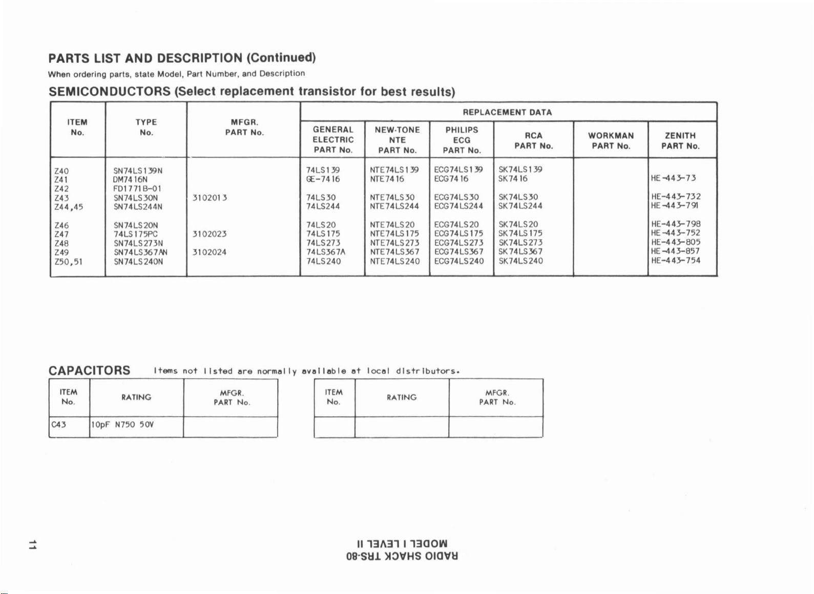
PARTS LIST AND DESCRIPTION (Continued)
When ordering parts, state Model, Part Number, and Description
SEMICONDUCTORS (Select replacement
ITEM TYPE MFGR.
No. No. PART No.
139N
Z40
Z41
Z42
Z43 SN74LS30N
Z44,45
Z46
Z47 74LS 175PC
Z48
Z49 SN74LS367N-4
Z50,51
CAPACITORS
ITEM
No.
SN74LS
DM7416N
FD17718-01
SN74LS244N
SN74LS20N
SN74LS273N
SN74LS240N
RATING
Items
3102013
3102023
3102024
not
lIsted
PART
MFGR.
ere
normelIyevelleble
No.
transistor
GENERAL
ELECTRIC
PART No.
74LS 139
~-7416
74LS30
74LS244
74LS20
74LS 175 NTE74LS 175
74LS273 NTE74LS273 ECG74LS273
74LS367A NTE74 LS367
74LS240
Iii
ITEM
No.
for
best results)
NEW·TONE
NTE
PART No. PART No.
NTE74LS 139 ECG74LS 139
NTE7416
NTE74LS30 ECG74LS30
NTE74LS244 ECG74LS244
NTE74LS20
NTE74LS240
et
locel
distrIbutors.
RATING
ECG7416 SK7416
ECG74LS20
ECG74LS175 SK74LS 175
ECG74LS367 SK74LS367
ECG74LS240
PHILIPS
ECG
REPLACEMENT DATA
RCA WORKMAN ZENITH
PART No.
SK74LS139
SK74LS30
SK74LS244
SK74LS20
SK74LS273
SK74LS240
MFGR.
PART
No.
PART No.
PART No.
HE-443-73
HE-443-732
HE-443-791
HE-443-798
HE
-443-752
HE-443-805
HE-443-857
HE-443-754
....
....
C43
10pF N750 50V
II
131\31
09·SHl
I
1300W
>t:)"HS OIO"H
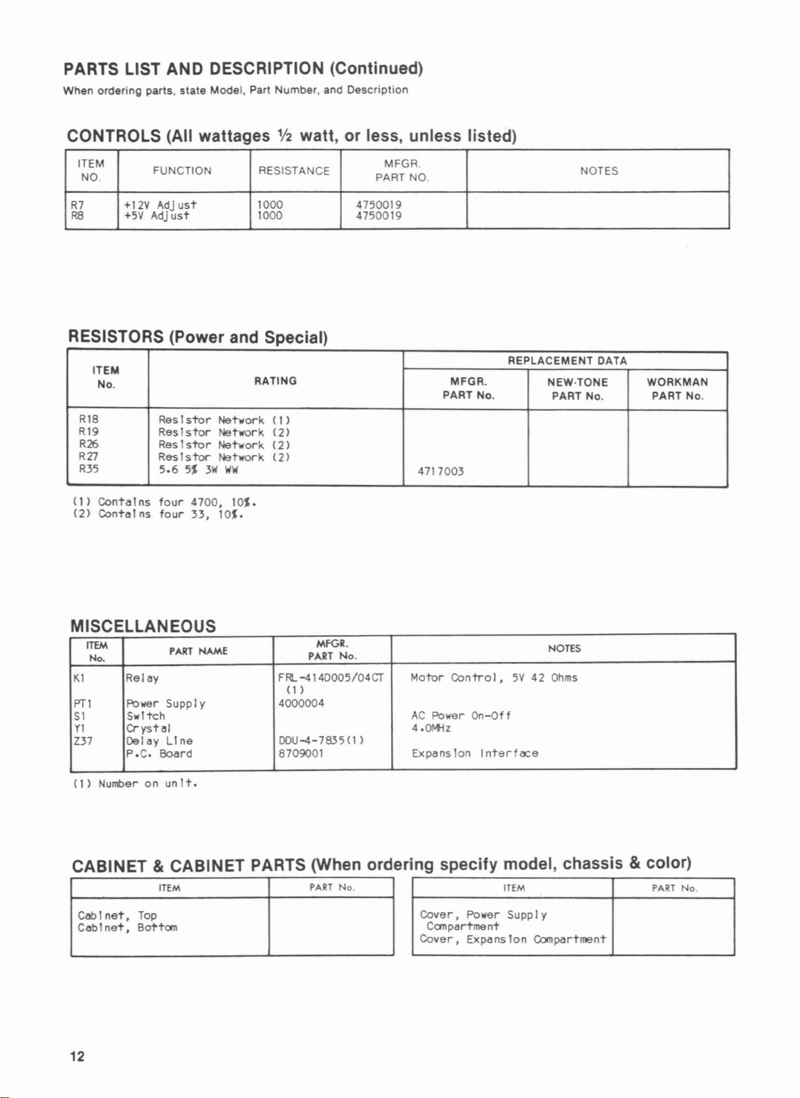
PARTS LIST AND DESCRIPTION (Continued)
When ordering parts, state Model, Part Number, and Description
CONTROLS (All wattages
R7
R8
ITEM
NO.
FUNCTION RESISTANCE
+12V Adj
+5V
Adj
ust
ust
Y2
watt,
1000 4750019
1000 4750019
RESISTORS (Power and Special)
R18
R19
R26
R27
R35
(1)
(2)
ITEM
No.
ContaIns
ContaIns
ResIstor
ResIstor
ResIstor
Res Is
5.6
5%
four
4700,
four
33,
tor
3'11
Network
Network
Network
Network
WW
10%.
10%.
RATING
(I)
(2)
(2)
(2)
or
less, unless listed)
MFGR.
PART NO.
MFGR.
PART No.
4717003
NOTES
REPLACEMENT DATA
NEW·TONE
PART No.
WORKMAN
PART No.
MISCELLANEOUS
ITEM
No.
Kl
Prl
SI
Yl
Z37
(I)
Relay
Power Suppl y
SwItch
Crystal
Del ayLIne
P.C.
NumberonunIt.
PART
Board
NAME
MFGR.
PART
No.
FRL
-414D005/04CT
(1)
4000004
DOU-4-7835<1 )
8709001
Motor
AC
4.0~z
Expans
CABINET & CABINET PARTS (When ordering
PART
No.
CabInet,
CabInet,
ITEM
Top
Bo1'tom
Control,
Power
On-Off
Ion
specify
Cover,
Cover,
Power
Compartment
ExpansIon
NOTES
5V42Ohms
Interface
model, chassis & color)
ITEM
Supply
Compartment
PART
No.
12

EXPANSION
INTERFACE
BOARD GridTrace
LOCATION GUIDE
Cl
C2
C3
C4
C5
C6
C7
C8
C9
Cl0
Cll
C12
C13
C14
C15
C16
C17
C18
C19
C20
C21
C22
C23
C24
C25
C26
C27
C28
C29
C30
C31
C32
C33
C34
C35
C36
C37
C38
C39
C40
C41
C42
C43
C44
C45
C46
C47
C48
C49
C50
C51
C52
C53
C54
C55
C56
C57
C58
C59
C60
C61
C62
C63
C64
C65
C66
C67
C68
C69
C70
C71
cn
cn
C-8
C-9
C-ll
C-12
C-13
C-14
C-15
C-17
F-8
E-9
F-l0
F-ll
E-ll
F-12
F-13
F-14
E-15
F-15
F-16
F-17
F-8
F-9
F-ll
F-12
F-13
F-14
F-15
F-17
H-8
H-9
H-l0
H-l1
H-ll
H-12
H-13
H-14
H-14
H-15
H-16
H-17
A-I
B-3
C-2
0-1
0-5
C-7
0-7
E-7
G-6
J-2
K-6
L-5
0-3
K-9
N-8
P-5
P-8
K-ll
K-15
N-15
B-17
C-17
K-17
M-18
0-18
Q-18
B-19
0-19
C-21
0-22
0-23
1-22
L-20
EXPANSION
C74
C75
C76
cn
C78
C79
CRI
CR2
CR3
CR4
J6
J7
1
A
B
c
D
G
H
K
L
M
N
o
p
Q
R
1
INTERFACE
M-21
N-22
C-25 Kl
G-25
1-25
L
-24
B-5
Q-3
K-16
K-8
A-16
A-13
J8
J9
Ql
Q2
Q3
Rl
R2
R3
R4
R5
R6
2
3
BOARD
4
A
HowordWSoms
A-II
Q-l
B-7
G-4 RIO
N-4
N-5
C-4
0-3
E-6
H-5 R
1-2
I
-4
R7
R8
R9
R11
R12
R13
R14
R15
R17
R
16
18
(§jli1Ji¥i'W
J-l
K-1
K-2
K-2
K-2
M-3
0-3
P-3
Q-4
K-5
0-5
I
-9
R19
R20
R21
R22
R23
R24
R25
R26
R27
R2B
R29
R30
Photo
1-9
K-10
L-14
A-18
C-18
A-18
C-18
E-19
H-19
K-20
0-24
E-24
R31
R32
R33
R34
R35
Yl
ZI
Z2
Z3
Z4
Z5
Z6
E-24
E-24
F-24
G-23
K-4
C-l
0-9
0-10
0-11
0-12
0-13
0-14
Z7
Z8
Z9
Z10
ZII
Z12
Z13
Z14
Z15
Z16
Z17
Z18
18
0-16
0-17
G-8
G-l0
G-l1
G-12
G-13
G-14
G-15
G-17
A-2
B-4
19
Z19
Z20
Z21
Z22
Z23
Z24
Z25
Z26
Z27
Z28
Z29
Z30
221
221
0-4
J-3
Q-4 Z33
O-{i Z34
F-6
H-{i Z36
J-6
L-{i
J-9
L-9
J-12
L-12
Z31
Z32
Z35
Z37
Z38
Z39
Z40
Z41
23
1
24
25
J
1
26 27
I
23124-125126127
J-16
L-16
A-19
C-19
E-19
G-19
L-19
N-19
P-19
R-18
C-22
Z42
Z43 L-21
Z44
Z45
Z46 B-25
Z47
Z48
Z49
Z50
Z51
EXPANSION
28
A
B
c
D
E
F
G
H
J
M
N
o
p
Q
R
28
F-22
0-21
0-23
0-25
F-25
H-25
J-25
L-25
INTERFACE
BOARD
::D
3::1>
2
0
0
0
m0
,...~
-:I>
""0
m"
<-4
~::D
_0
-0,
o
8
13
POWER SUPPLY
TROUBLESHOOTING
Disconnect the Power Supply
terface Board and check for 19.7VAC between pin 1 and pin
3ofConnector J9 and 23.6V between pin 2and pin 4ofConnector
J9. If the voltages are missing, check the cable and
connections at the Connector J9 and check for open AC
power cord. If the voltages are present, reconnect the
Power Supply to the Expansion Interface Board and turn
the Expansion Interface Board. Check
RegulatorIC(Z21),
-
5.OV
at the anodeofZener Diode
missing, check the Power Switch (Sl).
If
5.OV
is missing, check
associated
Regulator Drive Transistor (03) and pins 2 thru
13ofIC
justmentofthe5VAdjust
If the 11.9V is missing, check the voltages and
associated
thru7,10,11and 13ofIC Z20. If the 11.9V source is incorrect, check the adjustmentofthe
If
and check for a possible short to ground.
LINE PRINTER
If the Line Printer Connector (J4) is
run the following Basic program and use the
ceduretocheck the printer interface circuits. NOTE:Donot
connect a printertoConnector J4.
10
20
30
40
SO
60
70
Check for pulses at pin 1ofthe Tri-State
pulses are missing, check MUX (Multiplexer) IC
substitution.
one at a time, pins2,4,
that appears on the
to determine the correct number
X should equal
Pin 2ofZ49
Pin 4ofZ49
Pin 6ofZ49X=191
Pin 10ofZ49 X = 127
If any number is incorrect, check IC
Check
check
12,15,16
Z48, check IC Z48 by
pin11of
pulses at pin 4ofFlip/FlopIC(Z33).
a width
correct, check Capacitor C61, Resistors
check Flip/FlopICZ33 by
Z21. If the
the
5.OV
is missing, check Resistor
FOR Y = 1 TO
POKE 14312,0
POKE 14312,255
X = PEEK(14312)
NEXT Y
PRINT"X= "; X
GOTO
10
for
for
the waveform shown in Figure 2 at pins2,5,6,9,
and19of IC Z48. If any waveform is
IC Z48, check IC Z39 by
of
2!J.s.
11.9V at pin 3ofRegulator IC (Z20) and
with
Regulator Output Transistor (02) and
5.OV
with
Regulator Output Transistor (01) and pins 2
SO
Check the operationofIC Z49 by grounding,
Monitor
255
when none of the pins are grounded.
X=239
X=223
pulses at pin11of
substitution.Ifpulses are missing at
If the pulses are missingorthe
(PT1)
from the Expansion In-
On
for
5.OV
at pin 3
CR3.Ifall voltages are
the
voltages and components
7,10,11
source is incorrect, check the ad-
Control
6 and 10 and observe the number X
substitution.
(R8).
components
12V
Adjust Control (R7j).
R21,
Zener Diode CR3
not
operating, type and
following
BufferIC(Z49).
screen. Use the following chart
for
each pin. The number
Z49bysubstitution.
the Flip/FlopIC(Z48) and
missing
substitution.
The pulses should have
R23
and
(Z39)
at IC
Check for
width
is in-
R24
and
pro-
and
of
by
Figure 2
DISK DRIVE
If the Disk Drive Port (J5) is
clock
signal at pin24of
clockisoff
Capacitors C43 and C44 and ResistorsRland
clock
3ofFlip/Flop IC
check IC Z25 by
pin3,check the waveform at pin14of
the waveform is present at pin
tion.Ifthe waveform is missing at pin
substitution.
and ResistorsR1and
24ofIC Z42, type and run the following Basic program and
check
IC
(Z39).
10
FORX=14304TO14316 STEP 4
20
Y +
30
NEXT X
40
GOTO
If pulses are missing at anyofthe pins specified onICZ39,
check IC Z39 by
The Disk Drive
Drive should be On when the above program is running. If
the Disk Drive
at pin 5ofFlip/Flop IC
running). If the
by
If
substitution.Ifthe
for
pulses at pin 9ofIC Z41.Ifpulses are missing at pin
check IC Z39 by
check Capacitor C62, Resistors
Z33 by substituion.ICZ33 is a
Drive running for about 3 seconds
at pin 9ofIC Z33.
If the LED on the Disk Drive is not On when the program is
running, check for a High
IC
(Z47)
Z47 for Drive 2orpin15ofICZ47 for Drive3.If the reading
is correct, checkICZ41bysubstitution.
correct, check IC
If the Disk Drive is not reading, writing or the Head Stepping
Motor
check ICs
Z51) by
The operationofpins
by running the following Basic program and
valueofthe number X that appears on the
when a jumper is connected from groundtooneofthe pins.
frequency, check the 4.0MHz Crystal (Yl),
signal is missing at pin
(Z25).
substitution.
Check Crystal
for
pulses at pins4,5,7,9 and11of
PEEK(X):
is not running and the above
POKE X,255
10
substitution.
Motor
Motor
logic
substitution.
for
Drive0,pin 7 of IC
Z47bysubstitution.
Z32,
Z34,
substitution.
not
operating, check
the Disk Controller IC
24,
check the waveform at pin
If the waveform is present at pin
If the waveform is missing at
Counter IC
14,
check IC Z22 by substitu-
Yl,
R2.Ifthe
and the LED on the frontofthe Disk
is not running, check the
(Z33)
for
reading at pin 5 is High, check IC
logic
Z42
34,35and36ofICZ42
a High (while the program is
reading at pin 5 is Low, check
If pulses are present at pin
logic
reading at pin 2ofFlip/Flop
Z47
and Tri-State
14,
Capacitors C43 and C44
clock
signal is good at pin
Mux (Multiplexer)
R24
and
R25
timer
that keeps the Disk
after
a pulse is received
for Drive1,pin10of
If the reading is in-
circuit
Buffer
5V
5ms
OV
for
a 1MHz
(Z42).
If the
R2.
If the
3,
(Z22).
checkICZ19 by
logic
reading
Z41
and check IC
IC
checks are good,
ICs
(ZSO
and
can be checked
noting
the
Monitor
screen
If
9,
9,
14
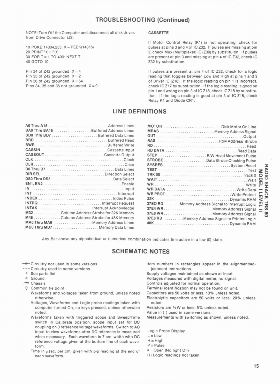
TROUBLESHOOTING (Continued)
NOTE: Turn
from Drive Connector (J3).
10
POKE 14304,255: X - PEEK(14316)
20
PRINT"X = ";X
30
FOR T = 1TO 400: NEXT T
40
GOTO
Pin34of
Pin35of
Pin36of
Pins
Off
the Computer and disconnect all
10
Z42 grounded X= 4
Z42
grounded X = 2
Z42
34,35and36not grounded X= 0
grounded X =
64
disk
drives
LINE DEFINITIONS
AO
Thru A15 Address Lines
BAO
Thru BA
BOO
Thru BD7 Buffered Data Lines
BRD
BWR Buffered Write
CASSIN Cassette Input
CASSOUT _ Cassette Output
CLK Clock
CLR Clear
DO
Thru07'"
DIR SEL Direction Select
DSO
Thru
EN1, EN2 Enable
IN
INT Interrupt
INDEX Index Pulse
INTRa
INTAK Interrupt Acknowledge
M32 Column Address Strobe
M48 Column Address Strobe for 48K Memory
MAO
MOO
15
DS3
Thru MA6 MemoryAddress Lines
Thru MD7 MemoryData Lines
Buffered Address Lines
Buffered
Interrupt Request
for
Read
Data Lines
Data Select
Input
32K Memory
CASSETIE
If
Motor
pulses at pins 3 and 4ofIC Z32. If pulses are
3,
are present at pin 3 and missing at pin 4ofIC Z32, checkIC
Z32 by
If pulses are present at pin 4ofIC Z32, check
reading that toggles between Low and High at pins 1and 3
of
check IC
pin 1and wrong on pin 3ofIC
tion. If the
RelayK1and Diode
MOTOR Disk
MRAS Memory Addess Signal
OUT
RAS
RD
RD
STEP
STROBE DataStrobe
SYSRES System Reset
TEST
TRK
WAIT , Wait
WR
WR
WR
32K Dynamic RAM
37EO
37E4
37E6
37E8
48K , Dynamic RAM
Control Relay
check Mux (Multiplexer) IC
substitution.
Driver IC
DATA Read Data
00
DATA Write Data
PROT Write Protect
(Z18).
Z17bysubstitution.
logic
............................•.............
RD
WR
WR
RD
Memory Address Signal to Interrupt Logic
(K1)
is not operating, check for
(Z39)
by substituion.Ifpulses
If the
logic
reading on pin 1 is incorrect,
If the
logic
reading is good at pin 3ofIC Z18, check
CR1.
Memory Address SignaltoPrinter Logic
Z18, checkICZ18 by substitu-
"
RIW
Head Movement Pulse
Memory Address Signal
Memory Address Signal
missing
reading is good on
MotorOnLine
Row Address Strobe
Clocking
at pin
foralogic
Output
Read
Pulse
Test
Track 0
Write
Any Bar above any alphabetical or numerical
SCHEMATIC NOTES
--Circuitry
- - -
Circuitry
e See parts
~
Ground
nm
Chassis
'9 Common tie point
Waveforms and voltages taken from ground, unless noted
Voltages, Waveforms and Logic probe readings taken with
Waveforms taken
Time in p.sec. per cm, given with
not used in some versions
used in some versions
list
otherwise.
computer
noted.
switch
coupling on 0 reference voltage waveforms. SwitchtoAC
input to view waveforms
when necessary. Each waveform is 7 cm.
reference voltage given at the
form.
each waveform.
turned On, no keys pressed, unless otherwise
with
triggered scope and SweepfTime
in Calibrate position, scope input set for
afterDCreference is measured
bottom
pop
width
lineofeach wave·
reading at the end of
combination
DC
with
DC
indicates line active in a low
Item numbers in rectangles appear in the alignment/ad-
justment
Supply voltages maintained as shown at input.
Voltages measured with digital meter,nosignal.
Controls adjusted for normal operation.
Terminal
Capacitors are50voltsorless, 10% unless noted.
Electrolytic capacitors are50volts or less, 20% unless
noted.
Resistors are
Value in ( ) used in some versions.
Measurements
Logic Probe Display
L=Low
H = High
P= Pulse
*= Open (No
(1)
Logic readings not taken.
instructions.
identification
Y2Worless, 5% unless noted.
light
with
may
switching
On)
(0)
state.
not
be foundonunit.
as shown, unless noted.
15
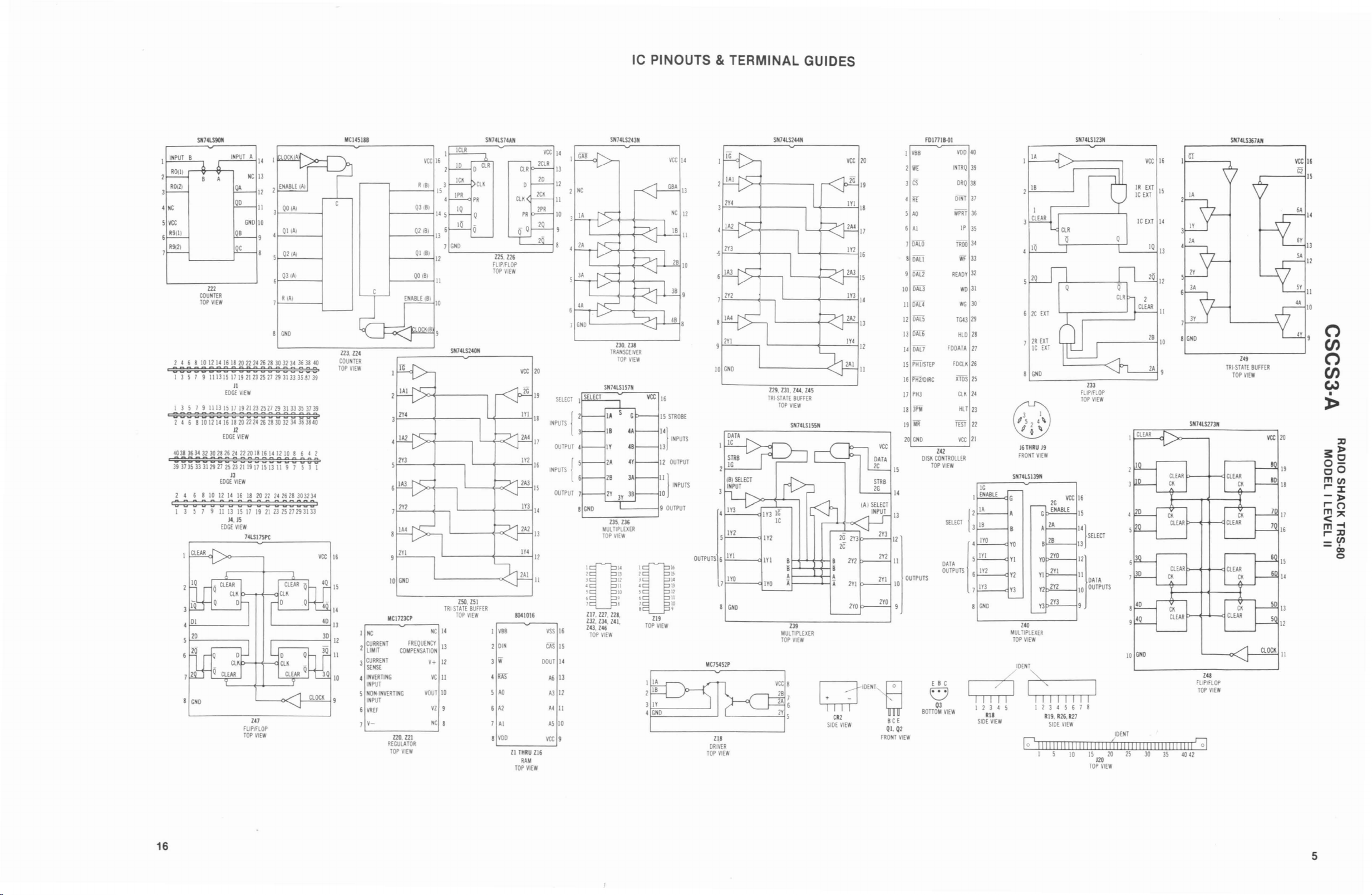
Ie
PINOUTS & TERMINAL GUIDES
S1114LS9Oll
NC
Real
4
NC
~
Yet
6
R9ill
R9(11
7
122
COU
1IR
TOP
lEW
1 4 6 8
10 121416 18
::::::::::::::::::::
I 3~7 9II13I~1719
I 3~7 9 II
::::::::::::::::::::
2 4 6 8
403836343230182624222018161412108642
::::::::::::::::::::
39
37~33
2 4 6 8
I:::::::::::::::::.
I 3~7 9 II13IS17192123 25
I
CLEAR
131~
101214161820
EDGE
31
19
21Z~232119171~
EDGE
10 121416 18
EDGE
13
Q.\
11
QO
11
GNO
10
QS
QC
202224
26 2830323436 38
Zl23
2~
Jl
EDGE
17
J2
J3
14
Z7
VIEW
1921
13
2~17
12242618303234363840
VIEW
13
VIEW
201224
IS
EW
74LSI1SPC
W
FliPIFLOP
TOP
VIEW
8
19
19
II 9 7
r--------''''j12
QO
Ql1AI
Q21AI
Q31AI
RIAl
GNO
3133
31
1628
171931
IAI
3H7J9
333~3739
~
3 I
303234
33
IS
14
13
11
11
10
Q2
I
VBB
11wr
3
CS
4
RE
5
AD
6
AI
7
DAlO
8
OAll
9
OAl2
10
om
II
OAt.
12
OALS
13
OAl6
14
OAl7
IS
PHIISTEP
16
PH2lOIRC
17
PH3
18
3PII
19
liR
20
GND
OUTPUTS
FOlnlB-G1
241
CO
01
TOP
E B C
o
03
BonOM
S"74lS123"
VDO
40
INTRQ
39
DRQ
38
OINT
37
WPRT
36
IP
3~
TROD
34
if
33
READY
31
we
31
WG30
VIEW
6lCEXT
71REXT
lC
EXT
8
GNO
J6THRU
J9
FRONT
VIEW
S1174LSI3911
vee
2G
ENABLE
G
A
1A
B
YO
VI
Y2
Y3
240
TIPLEXER
VIEW
1B
2YO
2Yl
2Y2
m
YO
YI
Y2
Y3
IIUL
TOP
I I I I I
I 2 3 4 5 6 7 8
R
19.
R26.
SIDE
lEW
f?
111111111111111111111
I
~
R27
10
233
FliPIFLOP
TOP
VIEW
16
I~
14}
SELECT
13
12
11
DATA
10
OUTPUTS
I~
TOP
120
20
VIEW
TG43
19
28
HLD
FOOATA
27
FOClK
26
XTDS
25
CLK
24
HLT
23
TEST
22
Yet
21
TROLLER
VIEW
IG
ENABLE
riA
SELECT
3
IB
4
IYO
SIYl
DATA
OUTPUTS
6
IY2
1Y3
7
8
GNO
d''"I~;,
I 1 3 4 5
VIEW
SIDE
RJI
Yet
16
:~:::
I~
lC
EXT
14
10
13
II
10
GND
10ENT
1111I1111111111111111
25
30 35
3A
8
GNO
S1174lS273"
ro]
4041
zu
FlIPIfLOP
TOP
VIEW
S1174lS367AJ1
m
TRI
STATE
BUFFER
TOP
VIEW
Yet
Yet
16
G2
IS
14
11
(')
4Y
9
en
(')
en
(,.)
•
~
20
::::c
~»
2
0
cO
men
'::I:
-»
'0
m"
<~
~::::c
_en
-0,
o
IIC14S11B
vee
16
R
lSI
3
IS
4
Q3
lSI
14
5
6
02
lSI
13
7
QIIBI
QO
m.m
COUNTER
40
TOP
lEW
V-
m
10
IICl123CP
FREQUENCY
COIIPENSA
Z20
221
REGUlATOR
TOP
VIEW
Yet
16
11
7
GND
12
IBI
II
S1174lS24Oll
L--------<f----:.:..:..j12
TRI
C
14
TlON
13
V+
12
VC
11
VOUT
10
V2
NC
IClR
10
IPR
IQ
10
250.
STATE
TOP
CLR
CLK
PR
0
Q
lSI
BUFFER
VIEW
S1174LS74AJ1
ill.
126
FliPIFLOP
TOP
VIEW
IIMIOl6
I
VBS
1
DIN
3
Vi
4m
~
AD
6
A2
7
AI
8
VOO
Z1
TOP
Yet
THRU
RAil
VIEW
216
20
19
13
II
Yet
lCLR
OOUT
.NPU
.
VSS
00
Ai>
AJ
A4
A~
Yet
14
SELECT
S {
OUTPUT
PUTS
{
OUTPUT
16
IS
14
13
12
11
10
9
1
4
7
8
S"74LS20"
DO.
238
TRANSCEIVER
TOP
VIEW
SN74lS1S7"
SELECT
lA
18
4A
IY
4B
4Y
2A
]A
2B
2Y
3Y
3B
GNO
ZJS
236
IIULTIPlEXER
'OP
VIEW
1
241
11
II
I
I
• U
,
•
1
a ,
I U
I
1[]1'
•
, 1,
. '
7
217.227.221.
n2,
234.
m.246
TOP
lEW
vee
16
IS
STROBE
14)
13
12
11}
10
9
OUTPUT
0
219
TOP
EW
11
II
INPUTS
OUTPUT
INPUTS
1
1\
l'
•
12
II
10
OUTPUTS
IIC7S4S2P
218
DRIVER
TOP
5
6
7
8
VIEW
III
IYl
lYO
GND
S1174lS244"
4----=..:.~18
L--------<f----:.:..:..j12
m.
231.
2«.
245
STATE
BUffER
TOP
EW
S"74LSlSS"
B
8 B
A
A
ZJ9
IIULTIPLEXER
TOP
VIEW
OIOENT
I
1YI
lYO
TRI
Y2
SIDE
B
A
A
CR2
Yet
VIEW
20
19
13
II
vee
BCE
01.
FROTVIEW
16
5

D'.,
1
PI' 1
-==-_------Z47
PI' 1
~.=L------Z48
11
9V~-----1
~F==j------~D''.
Z36
1
JJ
s::~
2
0
cO
m(J)
r-:::t
-~
r-n
m"
<~
~JJ
_(J)
-Co
o
EXPANSION INTERFACE BOARD
4
A
Howard
~
OV
W.
Sam.
lIIt·'III,II·t.!3;
Photo EXPANSION INTERFACE BOARD
17

r
I
I
I20VAC
I @
I '00""
I
I
I
,-
-----,
PTl
POWER
SlPPlY
,9
,
17
CR2
IlR-B:1O
pgl
PART
OF
51
I
J9
OFF
POWER
-ON
CS5
22001JF
9 E1600
01
REG
OOT
9R35
5.6
311
11.9Y
SOlflCE
•
PART
OF
51
POWER
OFF
-ON
o
PART
OF
51
POWER
OFF
-ON
L..-_~
CS7
...J
10.OOOIJF
~--:-:-=
EI600
Q2REG
OOT
RI2
.33
211
S.OY
SOlRCE
(")
C/)
(")
C/)
W
•
>
FOR
SEE
PHOTO
SCHEIlA
9 ItCl
~0~9U6
PART
OF
ZI9
He
3 2
~
9
He
7 6
S'OY
OY
1
He
ItCHO~9U6
PART
OF
He
ZI9
He
-t-r>:+
TERMINAL
PAGE
5.15.16
CIRCUITRACE
TIC CI
RCU
9
PART
9
PART
He
-tf4o
GUIDES
AND
..
m
/TRACE
..
[D]
ItCHO~9U8
OF
ZI9
ItCl~O~9U6
OF
ZI9
NOTES
10
::c
3:>
O~
cO
men
f"'"::I:
->
f"'"O
m"
<-4
~::c
_en
-cio
o
PART
OF
51
POWER
OFF
-ON
o
He
He
SH7~lSO~N
PART
OF
Z32
NC
He
~
I 12
NC
He
He
He
-S.OY
SOlRCE
~
A
~HOTorACT
IS>
HOWlTd W.
18
STANDARD NOTATION SCHEMATIC
WITH
li'·liih.".'"
sam.
& Co.•Inc.
1985
POWER
SUPPLY
POWER
SUPPLY
3

r-r+-
8.44
BA3
8A5
8.46
8.47
3?E~
I/R
PART
P
--+
I
'-------------------"""'T"-
PHOTO
CIRCUITRACE
SCt£HATlC
FOR
SEE
CABLINGl
HEAVY
USEOFMULTIPLE
LINE
ASSIGNED
A
~HOTO'ACT
© Howard
CIRCUITRACE
TERMINAL
PAGE
GUIDES
5,15,16
LINES
IDENTIFICATION
FOR
STANDARD
WITH
li'·"IIn·"'3'
W.
Sams & Co
c
,,[II]
AND
REDUCE
LINE
REFERENCE
NOTATION
..
Inc. 1985
oo--~
SN?4LSOON
OF
Z28
NOTES
SCHEMATIC
SN?4LSOON
PARTOF117
SN?4LSOON
PART
OF
r---"'-~-
R28
10K
2
5.O'i
Z28
SN?4LSOON
PART
OF
117
J20
00---<
01----«
02---<
03----«
05----«
07
8.40
8.41
8.42~
INT
__
SYRES---<
iN-----<.$..
_
OUT~
04---<
06---<
__
~
----«
-----(
NC----«
NC---<
NC----«
NC---<
NC----«
NC---<
28
J20
26
J20
32
J20
35_-<rr
J20
29
J20
22
J20
33
J20.c
21
J20
38
J20
18
J20
20
36·
J20
25
J20
27
J20
31
34
J20
30
J20
24
J20
..
J20
3?
J20
17
J20
19
EX?ANSIOH
BOARD
INTERNAL
EXPANSIOH
TO
Jl
~(---«
Jl
10
f-(---«
12
Jl
f-(---«
16
Jl
~(---«
20
Jl
~(----«9
24
Jl
f-(---«
28
Jl
f-(---«
32
Jl
~(---«
36
Jl
~(
40
J
~
3
1 5
J
7
J
~
1
1 13
J
5
1
J
9
J
.~
~
23
125
J
:-
~
27
129
J
:-
"
3
J
.~
35
1
J
19
J20 16
Jl
15
( (
14
J20
Jl
13
( (
18
J20 12
JI
II
( (
22 J20 10
Jl
f-(---«
26 J20 8
Jl
7
J 120
Jl
5
f-(---«
34 120 4
Jl
3
~
J20
---«
Jl
Jl
Jl
JI
Jl
21
Jl
Jl
Jl
I
1
9
J~
17
:-
:-
:-
:-
33
Jl
3?
CPU
IlOARO
CASSETTE
~
J20
J20
14
J20
J20
J20
EX?ANSIOH
J20
~
J20
J20
~
Jl
~NC
2
Jl
~NC
4
Jl
~NC
6
Jl
~NC
8
1----4~8
4 4
P3
5 5
f---7.~
P3
26
PART
J8
PART
J8
r~PART
8
PW
>-
2 2
INTERNAL
CASSIN
~
1::1
1::1
r:F
r:F
CASSIN
J?
5
1
TO
CASSETTE
2
CASSOUT~
~6
ENl~
OFdr-O+--'EN;~
I::l~
-13of1--
CLI(--_~oirt
ctR
__
NC
-+
J?
2
NC NC
NC
NC
NC
-+
NC
~--------J
NC NC NC
NC
J6
4
5
J6
1
-<J6
~
SN?4LS74AN
F
PIFL
TO
CASSETTE
1
v
5ms
OV
INTFlO
ctR
11
00416H
PART
tTo.---06
1'n---05
OF
134
___
I/R
_
I/R~
___
OIR
__
STEP~
___
I/R
RD
__
I/flEX
__
TRKOO
__
/'IOTM
_
050
_
051--7
_
DS2
_
053
--7)
1325
27
--7)
13
~
34
--~)
1331
35
--~)
1338
~
36
--7)
13
17
13
9
13
6
13
7
1330
2213
1332
13
2813
13
20
13~
13
2913
of
19
13
13
13
12
33
1323
1
13
16
13
13
~o
13
13
J3
11
)J3
~
J3
5
13
10
13
)
13
18
)
24
J3
8
)
21
S3
15
J3
I~
J3
2
~3
13
3
fIU'FERED
INTERFACE
IlJS
8.40
8.41~
B.42
8.43
8.4~
8A5~
8.46
8.47
8A8
8.49~
8.410--~
8.411~
8.412--~)
8.413~
8.4H--~)
8.415~
00
01---~)
.......
-------~
m.--------~
I?--------~
nr---------7
J4
DATA
DATA
DATA
DATA
DATA
DATA
DATA
DATA
1
2
3
4
5
6'
7
8
J4
3
5
J4
J4
7
9
J4
11
J4
13
J4
15
J4
17
02----7)
03---7~
J4~,..,....,==
DATASTflOIIE
TO
LINE
PRINTER
D~----7)
05---7)
06
rJ?---7)
J4
J4
16
J4
18
J4 J4
33
J4
8
12
J4
21
J~
25
04
:J4
22
J4
27
J4
31
J4
24
~
10
NC-7
NC~
NC-7
NC~
NC-7
NC~
J~
OUTOFPAPER
23
UNIT
J~
FAll.T
18
J4
25
J4
30
saECT
J4
19
J4
29
J4
32
05
06
rJ?
TRI-STATE
IJFFER
3?E6 I/R
~.JW
dJ
5.~
H:13
INT
IN
RD
1/R----7)
INTArC
----7)
OUT
-----'7)
5YSRfS )
-
~:!3
IIAIT~
- J7.:'l.
TE5T~
NC~
NC--~)
NC~
DATA
5EL-7
PROT
OATA-7
-7
-7
-7
--7
--7
--7
J5
-7
22
J5
2~
J5
18
J5
20
J5
-7
28
J5
30
J5
8
J5
25
J5
16
J5
10
J5
12
J5
1~
J5
32
J5
TO
DIS:
DRIVE
19
20
21
RADIO
SHACK
MODEL I LEVEL II
TRS·SO

CSCS3
If seal is broken, nonreturnable.
\ '
I
COMPUTERFACTSTM
put easy to use, informative technical
service information on the individual component,
The
features
• Preliminary Service Checks section is
experienced
following
contained
information
in this exclusive Soms COMPUTERFACTS
technician
or
is
just a
hobbyist,
sample
on
and
easy to use, step by step
even beginners.
of
the many
valuable
along
with some overall troubleshooting hints .
time saving
publication:
guide
data
for
the
right
at
•
Quick
and
your fingertips. Each edition includes specific
Comi>onent
component
Location
using the SAMS exclusive
photographs.
GRIOTRACE,
-
-
ORCUITRACE,
J
• SAMS
ORCUITRACE~,
famous
industry
GRIOTRACE
occeflted
~
11i
'.,
''''1
"*
I
waveforms,
Of
5111
...
SOl
•
standardized
voltages
on
..
Uti
._
I I
"
I I
notation
and
01
lolll"*"
T
""
ml
schematics
stage
containing
identification.
4
_.,.-,
5
6
• Stefl by Stefl Troubleshooting
procedures
to
quickly
,
MOCROO'ROCU"", e..
""'"
...
......
Ii'_
,
I .,..",
'''''
,""
\POft••"
'.
"Q.
1"0<.'_
,
__
".
"'-
""'.
_,_",_
.....h...
"""'
.....
locate
l.
lCl'\Il
'. """'_"'9 n, <_""'9 '''''
won'
'0
!IoIol"."'9
'
11 _ 13.."""
'n
'''''
.."....
''''O'''Ii'_1i'
'n
'_
...
oPlRA
"'"1....ICUIOOI
"0\1'"
,""
._.,
'n
.'9_'.
guides
the
problem.
TROUBLESHOOTING
'10"
_
0"'_
C ,
, 1
1
_
'Ii'
....
"'9'10'
I""
,
,ft
the technician
'''l~.''
,""
"",.
"._
<"'M'
-'
•••
Uo
_,,,
".
through
.....................
..
" .. "
..............
"
..
....................
.." " .
.1..-1.-'
..
.." . .
, . .
......
the necessary
~,
--~
.....
"
--'
....
-
....
,~
--
....
-
""
--'_
"",
,
..
•
Comfllete
shown when
gives you
Comflonents
possible.
many
replacements
Ports List in
SAMS
Distributor.
SEMICONDUCTORS (Select replacement
ITEM
No.
0102
010'
0201
~1
m"
(11!(ulh
fl..-
..
..n
TYPE
No
lSS~'
,--
IN(004<J>
ISS5> I
IS
0 reg'51ered
MFGR
PART
11(9-l"}16
I
U9-1S21
1201·'~
U9-lSlfi
lrodemork
NO
"G
PART
[cm19
[CGl09
ECG116
ECG~I9
of
Howofd
unique
to
tor
No
W
on
easy
semiconductor,
choose
best results)
GENERAL
ELECTRIC
PART
G[-SU
"."
OC·S04"
1X·~u
SOm$&Co,
No
10
use
from
MOTOROLA
PART
lN~9n
IN4(lQ.l
I
HI9S,
Inc
and
REPLACEMENT
No
format
is
"IE
PARI
NTn19
Nl[
109
NT[116
HTUl9
with
chip
and
available
DATA
RCA
NO
PARI
51(9091/1 n
"'''''
SIt»I]
51:9091/1//
.
field
replacements
IC cross-reference
at
".
No
your
WOf!KMAN
PART
l/(P'9?1/SI9
\1(1"
11(1'157
WEP9lS"19
No
""09
Electronic
ZENITH
PART
10'-l)l
IO}-Z9001
212-76-02
IOr!}l
No.
• Logic
Chart
components.
PIN
NO,
I
2 P
J
containing
IC
U'OO
P
P
PIN
NO,
21
22
2J
logic
IC
UIOO
P
P
P
probe
eo.
}<O.
I
2
J
L L L L L
P
readings
to
LOGIC
IC
UI02 UIO) UI04
" "
'IC
P P
IC IC IC
"
isolate
UIO~
P
"
defective
IC
UI06
P
Ul07
L L L
P
circuitry
Uloa
P P
" " "
IC
and
IC
UI09
"
(OMPUTERfA(TS
Rodio
To
$MIS
Howord
4300
Sho<:k
is 0 registered
order,
.•
W.
West
CSCS3
08933
ond
see
G.IOh4Cf
your Soms Representative,
Sam.
one
trodemork
&
Co.,
Trodemorks
62nd Street, PO.
of
Tandy
Inc.
Box
01
Howofd
Corporation,
W $oms &
CO,Inc
or
telephone 800-428-SAMS.
,
7092, Indianapolis, Indiana 46206 U.S.A.
ITT
 Loading...