

Page 1

RabbitCore RCM4100
C-Programmable Core Module
User’s Manual
019–0153 • 090508–G
Page 2

RabbitCore RCM4100
Digi International Inc.
www.rabbit.com
RabbitCore RCM4100 User’s Manual
Part Number 019-0153 • 090508–G • Printed in U .S.A.
©2006–2009 Digi International Inc. • All right s rese rved.
Digi International reserves the right to make changes and
improvements to its products without providing n otice.
T r ade mark s
Rabbit and Dynamic C are registered trademarks of Digi International Inc.
Rabbit 4000 and RabbitCore are trademarks of Digi International Inc.
No part of the contents of this manual may be reproduced or transmitted in any form or by any means
without the express written permission of Digi International.
Permission is granted to make one or more copies as long as the copyright page contained therein is
included. These copies of the manuals may not be let or sold for any reason without the express written
permission of Digi International.
The latest revision of this manual is available on the Rabbit Web s ite, www.rabb it.com,
for free, unregistered download.
Page 3

User’s Manual
TABLE OF CONTENTS
Chapter 1. Introduction 1
1.1 RCM4100 Features...............................................................................................................................2
1.2 Advantages of the RCM4100 ...............................................................................................................4
1.3 Development and Evaluation Tools......................................................................................................5
1.3.1 RCM4110 Development Kit.........................................................................................................5
1.3.2 RCM4100 Analog Development Kit............................................................................................6
1.3.3 Software........................................................................................................................................6
1.3.4 Online Documentation..................................................................................................................6
Chapter 2. Getting Started 7
2.1 Install Dynamic C.................................................................................................................................7
2.2 Hardware Connections..........................................................................................................................8
2.2.1 Step 1 — Prepare the Prototyping Board for Development..........................................................8
2.2.2 Step 2 — Attach Module to Prototyping Board............................................................................9
2.2.3 Step 3 — Connect Programming Cable......................................................................................10
2.2.4 Step 4 — Connect Power............................................................................................................11
2.3 Run a Sample Program.......................................................................................................................12
2.3.1 Troubleshooting..........................................................................................................................12
2.4 Where Do I Go From Here? ...............................................................................................................13
2.4.1 Technical Support.......................................................................................................................13
Chapter 3. Running Sample Programs 15
3.1 Introduction.........................................................................................................................................15
3.2 Sample Programs................................................................................................................................16
3.2.1 Serial Communication.................................................................................................................18
3.2.2 A/D Converter Inputs (RCM4100 only).....................................................................................21
3.2.2.1 Downloading and Uploading Calibration Constants.......................................................... 22
3.2.3 Real-Time Clock.........................................................................................................................24
Chapter 4. Hardware Reference 25
4.1 RCM4100 Digital Inputs and Outputs................................................................................................26
4.1.1 Memory I/O Interface.................................................................................................................32
4.1.2 Other Inputs and Outputs............................................................................................................32
4.2 Serial Communication ........................................................................................................................33
4.2.1 Serial Ports..................................................................................................................................33
4.2.1.1 Using the Serial Ports......................................................................................................... 34
4.2.2 Programming Port.......................................................................................................................35
4.3 Programming Cable............................................................................................................................36
4.3.1 Changing Between Program Mode and Run Mode....................................................................36
4.3.2 Standalone Operation of the RCM4100......................................................................................37
4.4 A/D Converter (RCM4100 only)........................................................................................................38
4.4.1 A/D Converter Power Supply.....................................................................................................40
Page 4

RabbitCore RCM4100
4.5 Other Hardware..................................................................................................................................41
4.5.1 Clock Doubler ............................................................................................................................41
4.5.2 Spectrum Spreader......................................................................................................................41
4.6 Memory..............................................................................................................................................42
4.6.1 SRAM.........................................................................................................................................42
4.6.2 Flash EPROM.............................................................................................................................42
Chapter 5. Software Reference 43
5.1 More About Dynamic C .....................................................................................................................43
5.2 Dynamic C Function Calls................................................................................................................45
5.2.1 Digital I/O...................................................................................................................................45
5.2.2 Serial Communication Drivers...................................................................................................45
5.2.3 SRAM Use..................................................................................................................................45
5.2.4 Prototyping Board Function Calls..............................................................................................47
5.2.4.1 Board Initialization............................................................................................................ 47
5.2.4.2 Alerts.................................................................................................................................. 48
5.2.5 Analog Inputs (RCM4100 only).................................................................................................49
5.3 Upgrading Dynamic C .......................................................................................................................66
5.3.1 Add-On Modules........................................................................................................................66
Appendix A. RCM4100 Specifications 67
A.1 Electrical and Mechanical Characteristics ........................................................................................68
A.1.1 A/D Converter...........................................................................................................................72
A.1.2 Headers......................................................................................................................................73
A.2 Rabbit 4000 DC Characteristics........................................................................................................74
A.3 I/O Buffer Sourcing and Sinking Limit.............................................................................................75
A.4 Bus Loading ......................................................................................................................................75
A.5 Jumper Configurations......................................................................................................................78
A.6 Conformal Coating............................................................................................................................80
Appendix B. Prototyping Board 81
B.1 Introduction .......................................................................................................................................82
B.1.1 Prototyping Board Features.......................................................................................................83
B.2 Mechanical Dimensions and Layout.................................................................................................85
B.3 Power Supply.....................................................................................................................................86
B.4 Using the Prototyping Board.............................................................................................................87
B.4.1 Adding Other Components........................................................................................................89
B.4.2 Measuring Current Draw...........................................................................................................89
B.4.3 Analog Features (RCM4100 only)............................................................................................90
B.4.3.1 A/D Converter Inputs........................................................................................................ 90
B.4.3.2 Thermistor Input............................................................................................................... 92
B.4.3.3 A/D Converter Calibration................................................................................................ 92
B.4.4 Serial Communication...............................................................................................................93
B.4.4.1 RS-232 .............................................................................................................................. 94
B.5 Prototyping Board Jumper Configurations........................................................................................95
Appendix C. Power Supply 99
C.1 Power Supplies..................................................................................................................................99
C.1.1 Battery Backup ..........................................................................................................................99
C.1.2 Battery-Backup Circuit............................................................................................................100
C.1.3 Reset Generator........................................................................................................................100
Index 103
Schematics 107
Page 5

User’s Manual 1
1. INTRODUCTION
The RCM4100 series is the first of the next-generation core
modules that take advantage of new Rabbit
®
4000 features such
as hardware DMA, clock speeds of up to 60 MHz, I/O lines
shared with up to six serial ports and four levels of alternate pin
functions that include variable-phase PWM, auxiliary I/O,
quadrature decoder, and input capture. Coupled with more than
500 new opcode instructions that help to reduce code size and
improve processing sp eed, this equates to a co re module that i s
fast, efficient, and the ideal solution for a wide range of embedded applications.
The Development Kit has the essentials that you need to design
your own microprocessor-based system, and includes a complete Dynamic C softw are development system. Th is Development Kit also contains a Prototyping Board that will al low you
to evaluate the RCM4100 series and to prototype circuits that
interface to the RCM4100 series of modules. You will also be
able to write and test software for these modules.
Throughout this manual, the term RCM4100 series refers to the complete series of
RCM4100 RabbitCore modules unless other production models are referred to specifically.
The RCM4100 has a Rabbit 4000 microprocessor operating at up to 58.98 MHz, static
RAM, flash memory, an 8-channel A/D converter, two clocks (main oscillator and timekeeping), and the circuitry necessary for reset and management of battery backup of the
Rabbit 4000’s internal real-time clock and the static RAM. One 50-pin header brings out
the Rabbit 4000 I/O bus lines, parallel ports, and serial ports.
The RCM4100 series receives its +3.3 V power from the customer-supplied motherboard
on which it is mounted. The RCM4100 series can interface with all kinds of CMOScompatible digital devices through the motherboard.
Page 6

2 RabbitCore RCM4100
1.1 RCM4100 Features
• Small size: 1.41" × 1.88" × 0.49"
(36 mm × 48 mm × 12 mm)
• Microprocessor: Rabbit 4000 running
at up to 58.98 MHz
• Up to 40 general-purpose I/O lines configurable with up to four alternate functions
• 3.3 V I/O lines with low-pow er mo des dow n to 2 kH z
•
Six CMOS-compatible serial ports — f
our ports are configurable as a clocked serial port
(SPI), and two ports are configurable as SDLC/HDLC serial ports.
• Alternate I/O bus can be configured for 8 data lines and 6 address lines (shared with
parallel I/O lines), I/O read/write
• 512K flash memory, 256K data SRAM
• Real-time clock
• Watchdog supervisor
Page 7
User’s Manual 3
There are three RCM4100 production models. Table 1 summarizes their main features.
The RCM4100 series is programmed ove r a stand ard PC US B port t hrough a p rogra mming
cable supplied with the Development Kit.
NOTE: The RabbitLink cannot be used to program RabbitCore modules based on the
Rabbit 4000 microprocessor.
Appendix A provides detailed specifications for the RCM4100 series.
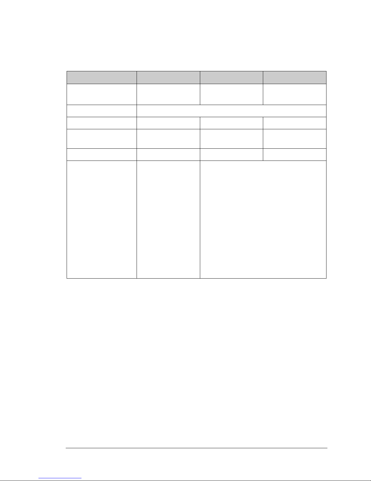
Table 1. RCM4100 Features
Feature RCM4100 RCM4110 RCM4120
Microprocessor
Rabbit
®
4000
at 58.98 MHz
Rabbit® 4000
at 29.49 MHz
Rabbit® 4000
at 58.98 MHz
Flash Memory 512K
Data SRAM 512K 256K 512K
Fast Program-Execution
SRAM
512K — 512K
A/D Converter 12 bits — —
Serial Ports
6 high-speed, CMOScompatible ports:
• all 6 configurable as
asynchronous (with
IrDA), 4 as clocked
serial (SPI), and 2 as
SDLC/HDLC
• 1 asynchronous
clocked serial port
shared with programming port
• 1 clocked serial port
shared with A/D converter
6 high-speed, CMOS-compatible ports:
• all 6 configurable as asynchronous (with IrDA),
4 as clocked serial (SPI), and 2 as SDLC/HDLC
• 1 asynchronous clocked serial port shar ed wit h
programming port
Page 8

4 RabbitCore RCM4100
1.2 Advantages of the RCM4100
• Fast time to market using a fully engineered, “ready-to-run/ready-to-program” microprocessor core.
• Competitive pricing when co mpare d with the alte rnati v e of purcha sing a nd asse mbli ng
individual components.
• Easy C-language program development and debugging
• Rabbit Field Utility to download compiled Dynamic C .bin files, and cloning board
options for rapid production loading of programs.
• Generous memory size allows large programs with tens of thousands of lines of code,
and substantial data storage.
Page 9
User’s Manual 5
1.3 Development and Evaluation Tools
1.3.1 RCM4110 Development Kit
The RCM4110 Development Kit contains the hardware essentials you will need to use
your RCM4110 module. The items in the Development Kit and their use are as follows.
• RCM4110 module.
• Prototyping Board.
• Universal AC adapter, 12 V DC, 1 A (includes Canada/Japan/U.S., Australia/N.Z.,
U.K., and European style plugs). Development Kits sold in North America ma y contain
an AC adapter with only a North American style plug.
• Programming cable with integrated level-matching circuitry.
•
10-pin header to DB9 serial cable.
• Dynamic C® CD-ROM, with complete product documentation on disk.
• Getting Started instructions.
• A bag of accessory parts for use on the Prototyping Board.
• Rabbit 4000 Processor Easy Reference poster.
• Registration card.
Figure 1. RCM4110 Development Kit
Rabbit and Dynamic C are registered trademarks of Rabbit Semiconductor Inc.
RabbitCore RCM4110
The RCM4110 RabbitCore module features 16-bit memory, allowing you to create a low-cost, low-power,
control solution for your embedded application. These Getting Started instructions included with the Development Kit will help you get your RCM4100 up and running so that you can run the sample programs to
explore its capabilities and develop your own applications.
Development Kit Contents
The RCM4110 Development Kit contains the following items:
• RCM4110 module.
• Prototyping Board.
• Universal AC adapter, 12 V DC, 1 A (includes Canada/Japan/U.S., Australia/N.Z., U.K., and European
style plugs). Development Kits sold in North America may contain an AC adapter with only a North
American style plug.
• Programming cable with integrated level-matching circuitry.
• 10-pin header to DB9 serial cable.
• Dynamic C
®
CD-ROM, with complete product documentation on disk.
• Getting Started instructions.
• Plastic and metal standoffs with 4-40 screws and washers.
• A bag of accessory parts for use on the Prototyping
Board.
• Rabbit 4000 Processor Easy Reference poster.
• Registration card.
Visit our online Rabbit store at www.rabbit.com/store/ for
the latest information on peripherals and accessories that
are available for all RCM4100 RabbitCore module models.
Installing Dynamic C
®
Insert the CD from the Development Kit in
your PC’s CD-ROM drive. If the installation
does not auto-start, run the setup.exe pro-
gram in the root directory of the Dynamic C
CD. Install any Dynamic C modules after you
install Dynamic C
.
Getting Started
Instructions
Prototyping Board
Accessory Parts for
Prototyping Board
Serial
Cable
Programming
Cable
D
1
R
1
PWR
DS1
GND
J1
U1
C1
GND
C2
J
P
1
C
3
D
2
J
P
2
C
4
+
3
.
3
V
J2
R
2
BT1
1
S1
RESET
R
X
D
T
X
D
T
X
C
R
X
C
G
N
D
J
4
U
X
2
9
RX81
R
X
8
7
C
X
4
1
RX83
RX11
C
X
3
9
UX30
UX10
UX12
UX14
UX16
RX79
C
X
2
9
C
X
1
7
RX67
U
X
4
5
R
X
8
5
GND
GND
GND
1
R24
R22
R21
R23
CX23
RX77
1
R
2
7
R
2
8
JP25
CX25
RX75
RX73
CX27
DS3
S3S2
DS2
J3
UX49
UX4
UX47
+5 V
GND
+3.3 V
RCM1
U
2
/RST_OUT
/IOWR
VBAT
EXT
PA1
PA3
PA5
PA7
PB1
PB3
PB5
PB7
PC1
PC3
PC5
PC7
PE1
PE3
PE5
PE7
PD1
LN1
PD3
LN3
PD5
LN5
PD7
LN7
VREF
GND
/IORD
/RST_IN
PA0
PA2
PA4
PA6
PB0
PB2
PB4
PB6
PC0
PC2
PC4
PC6
PE0
PE2
PE4
PE6
PD0
LN0
PD2
LN2
PD4
LN4
PD6
LN6
CVT
AGND
J
P
2
4
J
P
2
3
C
1
4
C
1
2
C
1
0
C8C7C
9
C
1
1
C
1
3
R10
R8R6R4R3R5R
7
R20
R
1
8
R
1
6
R
1
4
R
1
3
R
1
5
R
1
7
R29
J
P
1
1
J
P
1
5
J
P
1
9
J
P
2
1
J
P
2
2
J
P
2
0
J
P
1
7
J
P
1
3
R19
R9
RX57
RX55
RX97
RX49
U
X
3
3
U
X
3
1
R
X
8
9
UX3
U
X
3
7
U
X
4
2
U
X
4
1
R
X
6
3
R
X
6
5
R
X
6
1
RX59
R
2
6
R25
Q1
C15
C
1
9
C
2
0
U3
C18
C
1
7
JP16
JP6
JP5
JP12
JP4
JP3
JP14
JP8
JP7
JP18
JP9
JP10
C16
L1
C6
C5
A
G
N
D
C
V
T
L
N
6
I
N
L
N
4
I
N
L
N
2
I
N
L
N
0
I
N
V
R
E
F
L
N
7
I
N
L
N
5
I
N
L
N
3
I
N
L
N
1
I
N
A
G
N
D
A
G
N
D
R
1
1
R
1
2
R
X
4
7
RX43
Universal
AC Adapter
with Plugs
C20
L1
C21
R5
R6
R7
R8
R9
R10
R11
R12
R13
C9
C10
C11
C12
C13
C14
C15
C16
RP1
JP6
JP5
R
20
JP4
C3
U4
TP2
J1
R38
R2
R1
U1
C8
C1
U2
C5
C4
R3
U3
R37
R21
U5
C17
C18
C52
C56
R23
R22
U6
JP3
R
41
C6C7R4
U9
C53
1
40
41
80
PROG
DIAG
Page 10

6 RabbitCore RCM4100
1.3.2 RCM4100 Analog Development Kit
The RCM4100 Analog Development Kit contains the hardware essentials you will need to
use the RCM4100 module. The RCM4100 Analog Development Kit contents are similar
to those of the RCM4110 Development Kit, except that the RCM4100 module is included
instead of the RCM4110 module.
1.3.3 Software
The RCM4100 series is programmed using version 10.01 or later of Dynamic C.
A compat-
ible version is included on the Developm ent Kit CD-RO M .
Starting with Dynamic C version 10.40, Dynamic C includes the popular µC/OS-II realtime operating system, point-to-point protocol (PPP), FAT file system, RabbitWeb, and
other select libraries. Rabbit also offers for purchase the Rabbit Embedded Security Pack
featuring the Secure Sockets Layer (SSL) and a specific Advanced Encryption Standard
(AES) library.
In addition to the Web-based technical support included at no extra charge, a one-year
telephone-based technical support module is also available for purchase. Visit our Web
site at www.rabbit.com or contact your Rabbit sales representative or authorized distribu-
tor for further information.
1.3.4 Online Documentation
The online documentation is installed along with Dynamic C, and an icon for the documentation menu is placed on the workstation’s desktop. Double-click this icon to reach the
menu. If the icon is missing, use your browser to find and load
default.htm in the docs
folder, found in the Dynamic C installation folder.
The latest versions of all documents are always available for free, unregistered download
from our Web sites as well.
Page 11

User’s Manual 7
2. GETTING S TARTED
This chapter de scribes the RC M4100 series in more detail, an d
explains how to set up and use the accompanying Prototyping Board.
NOTE: This chapter (and thi s manual) assume that you have t he RCM4100 Development
Kit. If you purchased an RCM4100 module by itself, you will have to adapt the information in this chapter and elsewhere to your test and development setup.
2.1 Install Dynamic C
To develop and debug programs for the RCM4100 series (and for all other Rabbit hardware), you must install and use Dynamic C.
If you have not yet installed Dynamic C version 10.01 (or a later version), do so now by
inserting the Dynamic C CD from the RCM4100 Development Kit in your PC’ s CD-ROM
drive. If autorun is enabled, the CD installation will begin automatically.
If autorun is disabled or the installation does not start, use the Windows Start | Run menu
or Windows Disk Explorer to launch setup.exe from the root folder of the CD-ROM.
The installation program will guide you through the installation process. Most steps of the
process are self-explanatory.
Dynamic C uses a COM (serial ) port to c ommunica te with the tar get developme nt syste m.
The installation allows you to choose the COM port that will be used. The default selection is COM1. You may select any available port for Dynamic C’s use. If you are not certain which port is available, select COM1. This selection can be changed later within
Dynamic C.
NOTE: The installation utility does not check the selected COM port in any way. Speci-
fying a port in u se by a nother device (mouse, modem, etc.) may lead to a message such
as "could not open serial port" when Dynamic C is started.
Once your installation is complete, you will have up to three new icons on your PC desktop. One icon is for Dynamic C, one opens the documentation menu, and the third is for
the Rabbit Field Utility, a tool used to download precompiled software to a target system.
If you have purchased any of the optional Dynamic C modules, install them after installing
Dynamic C. The modules may be installed in any order. You must install the modules in
the same directory where Dynamic C was installed.
Page 12
8 RabbitCore RCM4100
2.2 Hardware Connections
There are three steps to connecting the Prototyping Board for use with Dynamic C and the
sample programs:
1. Prepare the Prototyping Board for Development.
2. Attach the RCM4100 module to the Prototyping Board.
3. Connect the programming cable between the RCM4100 and the PC.
4. Connect the power supply to the Prototyping Board.
2.2.1 Step 1 — Prepare the Prototyping Board for Development
Snap in four of the plastic standoffs supplied in the bag of accessory parts from the Development Kit in the holes at the corners as shown.
Figure 2. Insert Standoffs
D
1
R
1
PWR
DS1
GND
J1
U1
C1
GND
C2
JP
1
C
3
D
2
JP
2
C
4
+
3.3 V
J2
R
2
BT1
1
S1
RESET
R
XD
TX
D
TX
C
R
XC
G
N
D
J4
UX
29
RX81
R
X
87
C
X41
RX83
RX11
C
X
39
UX30
UX10
UX12
UX14
UX16
RX79
C
X
29
C
X17
RX67
U
X45
RX
85
GND
GND
GND
1
R24
R22
R21
R23
CX23
RX77
1
R27R
28
JP25
CX25
RX75
RX73
CX27
DS3
S3S2
DS2
J3
UX49
UX4
UX47
+5 V
GND
+3.3 V
RCM1
U
2
/RST_OUT
/IOWR
VBAT
EXT
PA1
PA3
PA5
PA7
PB1
PB3
PB5
PB7
PC1
PC3
PC5
PC7
PE1
PE3
PE5
PE7
PD1
LN1
PD3
LN3
PD5
LN5
PD7
LN7
VREF
GND
/IORD
/RST_IN
PA0
PA2
PA4
PA6
PB0
PB2
PB4
PB6
PC0
PC2
PC4
PC6
PE0
PE2
PE4
PE6
PD0
LN0
PD2
LN2
PD4
LN4
PD6
LN6
CVT
AGND
JP24JP
23
C14C12C
10
C8C7C
9
C
11
C
13
R10
R8R6R4R3R5R
7
R20
R18R16R14R13R15R
17
R29
JP11JP15JP19JP21JP22
JP20
JP17
JP
13
R19
R9
RX57
RX55
RX97
RX49
U
X33U
X
31
R
X
89
UX3
U
X
37
U
X
42
U
X
41
R
X
63
R
X
65
R
X
61
RX59
R
26
R25
Q1
C15
C
19
C
20
U3
C18
C
17
JP16
JP6
JP5
JP12
JP4
JP3
JP14
JP8
JP7
JP18
JP9
JP10
C16
L1
C6
C5
AG
N
D
C
V
T
LN
6INLN4INLN2INLN0IN
V
R
E
F
LN
7INLN5INLN3INLN1IN
A
G
N
D
A
G
N
D
R
11
R
12
R
X
47
RX43
Page 13

User’s Manual 9
2.2.2 Step 2 — Attach Module to Prototyping Board
Turn the RCM4100 module so that the mounting holes line up with the corresponding
holes on the Prototyping Board. Insert the m et al st an d offs as shown, secure them from the
bottom using two screws and washers, then insert the module’s header J2 on the bottom
side into socket RCM1 on the Prototyping Board.
Figure 3. Install the Module on the Prototyping Board
NOTE: It is important that you line up the pins on header J2 of the module exactly with
socket RCM1 on the Pr ototyp ing Boa rd. The header pins may bec ome b ent or da maged
if the pin alignment is offset, and the module will not work. Permanent electrical damage to the module may also result if a misaligned module is powered up.
Press the module’s pins gently into the Prototyping Board socket—press down in the area
above the header pins. For additional integrity, you may secure the RCM4100 to the standoffs from the top using the remaining two screws and washers.
D1
R1
PWR
DS1
GND
J1
U1
C1
GND
C2
JP1
C3
D2
JP2
C4
+3.3 V
J2
R2
BT1
1
S1
RESET
RXD TXD
TXC RXC
GND
J4
UX29
RX81
RX87
CX41
RX83
RX11
CX39
UX30
UX10
UX12
UX14
UX16
RX79
CX29
CX17
RX67
UX45
RX85
GND
GND
GND
1
R24
R22
R21
R23
CX23
RX77
1
R27
R28
JP25
CX25
RX75
RX73
CX27
DS3
S3S2
DS2
J3
UX49
UX4
UX47
+5 V
GND
+3.3 V
RCM1
U2
/RST_OUT
/IOWR
VBAT
EXT
PA1
PA3
PA5
PA7
PB1
PB3
PB5
PB7
PC1
PC3
PC5
PC7
PE1
PE3
PE5
PE7
PD1
LN1
PD3
LN3
PD5
LN5
PD7
LN7
VREF
GND
/IORD
/RST_IN
PA0
PA2
PA4
PA6
PB0
PB2
PB4
PB6
PC0
PC2
PC4
PC6
PE0
PE2
PE4
PE6
PD0
LN0
PD2
LN2
PD4
LN4
PD6
LN6
CVT
AGND
JP24
JP23
C14
C12
C10
C8C7C9
C11
C13
R10
R8R6R4R3R5
R7
R20
R18
R16
R14
R13
R15
R17
R29
JP11
JP15
JP19
JP21
JP22
JP20
JP17
JP13
R19
R9
RX57
RX55
RX97
RX49
UX33UX31
RX89
UX3
UX37 UX42
UX41
RX63
RX65
RX61
RX59
R26
R25
Q1
C15
C19 C20
U3
C18
C17
JP16
JP6
JP5
JP12
JP4
JP3
JP14
JP8
JP7
JP18
JP9
JP10
C16
L1
C6
C5
AGND
CVT
LN6IN
LN4IN
LN2IN
LN0IN
VREF
LN7IN
LN5IN
LN3IN
LN1IN
AGND
AGND
R11
R12
RX47
RX43
RCM4100
RCM1
R1
J1
R2
R5
R4
R3
JP1
JP2
JP9
JP6
JP7
JP3
JP5
JP4
C4
C3
C2
L1
C1
R7
R8
R6
R10
R9
U1
U2
R11
C15
RP2
C16
C17
D1
R27
RP1
R15
C23
R17
R16
C21
C14
U6
R19
R18
R22
R23
Y2
C27
U7
C28
R21
JP8
JP10
JP11
JP12
C5
Y1
Q1
C6
C7
C8
C9
C10 C11
U5
C12
C13
R12
C24
R14
C25
C26
C19
C20
U4
U3
C18
R13
C30
C31
C34 C35
C32
C33
C29
C38
C39
C37
C36
Line up mounting
holes with holes
on Prototyping Board.
Insert standoffs
between
mounting holes and
Prototyping Board.
Page 14
10 RabbitCore RCM4100
2.2.3 Step 3 — Connect Programming Cable
The programming cable connects the module to the PC running Dynamic C to download
programs and to monitor the module during debugging.
Connect the 10-pin connector of the programming cable labeled
PROG to header J1 on
the RCM4100 as shown in Figure 4. Be sure to orient the marked (usually red) edge of the
cable towards pin 1 of the connector. (Do not use the DIAG connector , which is used for a
normal serial connection.)
Figure 4. Connect Programming Cable and Power Supply
NOTE: Never disconnect the programming cable by pulling on the ribbon cable.
Carefully pull on the connector to remove it from the header.
NOTE: Either a serial or a USB programmin g cab le was su pplie d with th is Developmen t
Kit. If you have a serial programming cable, an RS-232/USB converter (Rabbit Part
No. 20-151-0178) is available to allow you to use the serial programming cable with a
USB port.
Depending on the programming cable, connect the other end to a COM port or a USB port
on your PC.
D1
R1
PWR
DS1
GND
J1
U1
C1
GND
C2
JP1
C3
D2
JP2
C4
+3.3 V
J2
R2
BT1
1
S1
RESET
RXD TXD
TXC RXC
GND
J4
UX29
RX81
RX87
CX41
RX83
RX11
CX39
UX30
UX10
UX12
UX14
UX16
RX79
CX29
CX17
RX67
UX45
RX85
GND
GND
GND
1
R24
R22
R21
R23
CX23
RX77
1
R27
R28
JP25
CX25
RX75
RX73
CX27
DS3
S3S2
DS2
J3
UX49
UX4
UX47
+5 V
GND
+3.3 V
RCM1
U2
/RST_OUT
/IOWR
VBAT
EXT
PA1
PA3
PA5
PA7
PB1
PB3
PB5
PB7
PC1
PC3
PC5
PC7
PE1
PE3
PE5
PE7
PD1
LN1
PD3
LN3
PD5
LN5
PD7
LN7
VREF
GND
/IORD
/RST_IN
PA0
PA2
PA4
PA6
PB0
PB2
PB4
PB6
PC0
PC2
PC4
PC6
PE0
PE2
PE4
PE6
PD0
LN0
PD2
LN2
PD4
LN4
PD6
LN6
CVT
AGND
JP24
JP23
C14
C12
C10
C8C7C9
C11
C13
R10
R8R6R4R3R5
R7
R20
R18
R16
R14
R13
R15
R17
R29
JP11
JP15
JP19
JP21
JP22
JP20
JP17
JP13
R19
R9
RX57
RX55
RX97
RX49
UX33UX31
RX89
UX3
UX37 UX42
UX41
RX63
RX65
RX61
RX59
R26
R25
Q1
C15
C19 C20
U3
C18
C17
JP16
JP6
JP5
JP12
JP4
JP3
JP14
JP8
JP7
JP18
JP9
JP10
C16
L1
C6
C5
AGND
CVT
LN6IN
LN4IN
LN2IN
LN0IN
VREF
LN7IN
LN5IN
LN3IN
LN1IN
AGND
AGND
R11
R12
RX47
RX43
R1
J1
R2
R5
R4
R3
JP1
JP2
JP9
JP6
JP7
JP3
JP5
JP4
C4
C3
C2
L1
C1
R7
R8
R6
R10
R9
U1
U2
R11
C15
RP2
C16
C17
D1
R27
RP1
R15
C23
R17
R16
C21
C14
U6
R19
R18
R22
R23
Y2
C27
U7
C28
R21
JP8
JP10
JP11
JP12
C5
Y1
Q1
C6
C7
C8
C9
C10 C11
U5
C12
C13
R12
C24
R14
C25
C26
C19
C20
U4
U3
C18
R13
C30
C31
C34 C35
C32
C33
C29
C38
C39
C37
C36
RESET
AC Adapter
Remove slot cover,
insert tab into slot
Snap plug into place
2
1
Assemble
AC Adapter
3-pin
power connector
J1
Colored
edge
To
PC COM port
or USB port
PROG
DIAG
Programming
Cable
PROG
J1
Page 15

User’s Manual 11
If you are using a USB programming cable, your PC should recognize the new USB hardware, and the LEDs in the shrink-wrapped area of the programming cable will flash — if
you get an error message, you will have to install USB drivers. Drivers for Windows XP
are available in the Dynamic C Drivers\Rabbit USB Programming Cable\
WinXP_2K
folder — double-click DPInst.exe to install the USB drivers. Drivers for
other operating systems are available online at www.ftdichip.com/Drivers/VCP .htm.
2.2.4 Step 4 — Connect Power
Once all the other connections have been made, you can connect power to the Prototyping
Board.
If you have the universal AC adapter , prepare the AC adapter for the country where it will
be used by selecting the appropriate plug. Insert the top of the plug assembly into the slot at
the top of the AC adapter as shown in Figure 4, then press down on the plug until it clicks
into place.
Connect the AC adapter to 3-pin header J1 on the Prototyping Board as shown in Figure 4
above. The connector may be attached either way as long as it is not offset to one side—
the center pin of J1 is always connected to the positive terminal, and either edge pin is
ground.
Plug in the AC adapter. The PWR LED on the Prototyping Board next to the power connector at J1 should light up. The RCM4100 and the Prototyping Board are now ready to be
used.
NOTE: A RESET button is provided on the Pro totyping Boar d next to t he batter y holder
to allow a hardware reset without disconnecting power.
To power down the Prototyping Board, unplug the power connector from J1. You should
disconnect power before making any circuit adjustments in the prototyping area, changing
any connections to the board, or removing the RCM4100 from the Prototyping Board.
Page 16

12 RabbitCore RCM4100
2.3 Run a Sample Program
Once the RCM4100/RCM4110 is connected as described in the preceding pages, start
Dynamic C by double-clicking on the Dynamic C icon on your desktop or in your
Start
menu.
If you are using a USB port to connect your computer to the RCM4100/RCM4110, click
on the “Communications” tab and verify that
Use USB to Serial Converter is selected to
support the USB programming cable. Click
OK. You may have to determine which COM
port was assigned to the RS-232/USB converter. Open
Control Panel > System > Hard-
ware > Device Manager > Ports
and identify which COM port is used for the USB con-
nection. In Dynamic C, select
Options > Project Options, then select this COM port on
the
Communications tab, then click OK. You may type the COM port number followed by
Enter on your computer keyboard if the COM port number is outside the range on the drop-
down menu.
Now find the file PONG.C, which is in the Dynamic C SAMPLES folder. To run the pro-
gram, open it with the
File menu, compile it usin g the Compile menu, and then run it by
selecting
Run in the Run menu. The STDIO window will open on your PC and will dis-
play a small square bouncing around in a box.
2.3.1 Troubleshooting
If Dynamic C appears to compile the BIOS successfully, but you then receive a communication error message when you compile and load a sample program, it is possible that your
PC cannot handle the higher program-loading baud rate. Try changing the maximum
download rate to a slower baud rate as follows.
• Locate the Serial Options dialog in the Dynamic C Options > Project Options >
Communications
menu. Select a slower Max download baud rate.
If a program compiles and loads, but then loses target communication before you can
begin debugging, it is possible that your PC cannot handle the default debugging baud
rate. Try lowering the debugging baud rate as follows.
• Locate the
Serial Options dialog in the Dynamic C Options > Project Options >
Communications
menu. Choose a lower debug baud rate.
If you receive the message
No Rabbit Processor Detected, the programming cable
may be connected to the wrong COM port, a connection may be faulty, or the target system may not be powered up. First, check to see that the power LED on the Prototyping
Board is lit and that the jumper across pins 5–6 of header JP10 on the Prototyping B oard is
installed. If the LED is lit, check both ends of the programming cable to ensure that it is
firmly plugged into the PC and the programming header on the RCM4100 wi th the marked
(colored) edge of the programming cable tow ards pin 1 of the programming header . Ensure
that the module is firmly and correctly installed in its connectors on the Prototyping Board.
If there are no faults with the hardware, select a different COM port within Dynamic C as
explained for the USB port above. Press <Ctrl-Y> to force Dynamic C to r ecom pile the
BIOS. If Dy n a mic C still reports it is unable to locate the target sys tem, repeat the above
steps for another av ail able C OM po rt. You should receive a
Bios compiled success-
fully
message once this step is completed successfully.
Page 17

User’s Manual 13
2.4 Where Do I Go From Here?
If the sample program ran fine, you are now ready to go on to the sample programs in the
RCM4100 User’s Manual (click the documentation icon on your PC) and to develop your
own applications. The sa mple prog rams
can be easily modified for your own use. The user's
manual also provides complete hardware reference infor mation and software funct ion calls for
the RCM4100 and the Prototyping Board.
For advanced development topics, refer to the Dynamic C User’s Manual, also in the
online documentation set, which is on the Dynamic C CD in a docs folder..
2.4.1 Technical Support
NOTE: If you purchased your RCM4100 t hrough a di strib utor or thr ough a Rabbi t partn er,
contact the distrib utor or partner first for tec hnical support.
If there are any problems at this point:
• Use the Dynamic C
Help menu to get further assistance with Dynamic C.
• Check the Rabbit Technical Bulletin Board and forums at www.rabbit.com/support/bb/
and at www.rabbit.com/forums/.
• Use the Technical Support e-mail form at www.rabbit.com/support/.
Page 18

14 RabbitCore RCM4100
Page 19

User’s Manual 15
3. RUNNING SAMPLE PROGRAMS
To develop and debug programs for the RCM4100 series (and
for all other Rabbit hardware), you must install and use
Dynamic C. This chapter provides a tour of its major features
with respect to the RCM4100 series.
3.1 Introduction
T o help familiarize you with the RCM4100 series of modules, Dynamic C includes several
sample programs. Loading, executing and studying these programs will give you a solid
hands-on overview of the RCM4100 series’ capabilities, as well as a quick start with
Dynamic C as an application development tool.
NOTE:
The sample progr ams assum e that you ha ve at lea st an e lemen tary gr asp of A NSI C.
If you do not, see the introductory pages of the Dynamic C User’s Manual for a sug-
gested reading list.
In order to run the sample programs discussed in this chapter and elsewhere in this manual,
1. Your module must be plugged in to the Prototyping Board as described in Chapter 2,
“Getting Started.”
2. Dynamic C must be installed and running on your PC.
3. The programming cable must connect the programming header on the module to your
PC.
4. Power must be applied to the module through the Prototyping Board.
Refer to Chapter 2, “Getting Started,” if you need further information on these steps.
To run a sample program, open it with the
File menu (if it is not still open), then compile
and run it by pressing F9.
Each sample program has comments that describe the purpose and function of the pro-
gram. Follow the instructions at the beginning of the sample program.
More complete information on Dynamic C is provided in the Dynamic C User’s Manual.
Page 20
16 RabbitCore RCM4100
3.2 Sample Programs
Of the many sample programs included with Dynamic C, several are specific to the
RCM4100 series of modules. These programs will be found in the SAMPLES\RCM4100
folder.
• CONTROLLED.C—Demonstrates use of the digital outputs by having you turn LEDs
DS2 and DS3 on the Prototyping Board on or off from the STDIO window on your PC.
Parallel Port B bit 2 = LED DS2
Parallel Port B bit 3 = LED DS3
Once you compile and run CONTROLLED.C, the following display will appear in the
Dynamic C STDIO window.
Press “2” or “3” on your keyboard to select LED DS2 or DS3 on the Prototyping
Board. Then follow the prompt in the Dynamic C
STDIO window to turn the LED ON
or OFF. A logic low will light up the LED you selected.
• FLASHLED1.C—demonstrates the use of assembly language to flash LEDs DS2 and
DS3 on the Prototyping Board at different rates. Once you have compiled and run this
program, LEDs DS2 and DS3 will flash on/off at different rates.
•
FLASHLED2.C—demonstrates the use of cofunctions and costatements to flash LEDs
DS2 and DS3 on the Prototyping Board at different rates. Once you have compiled and
run this program, LEDs DS2 and DS3 will flash on/off at different rates.
Page 21

User’s Manual 17
• LOW_POWER.C—demonstrates how to implement a function in RAM to reduce power
consumption by the Rabbit microprocessor . There are four features that lead to the lowest possible power draw by the microprocessor.
1. Run the CPU from the 32 kHz crystal.
2. Turn off the high-frequency crystal oscillator.
3. Run from RAM.
4. Ensure that internal I/O instructions do not use CS0.
Once you are ready to compile and run this sample program, use <Alt-F9> instead of
just
F9. This will disable polling, which will allow Dynamic C to continue debugging
once the target starts running off the 32 kHz oscillator.
This sample program will toggle LEDs DS2 and DS3 on the Prototyping Board. You
may use an oscilloscope. DS2 will blink the fastest. After switching to low power , both
LEDs will blink together.
• TAMPERDETECTION.C—demonstrates how to detect an attempt to enter the bootstrap
mode. When an attempt is detected, the battery-backed onchip-encryption RAM on the
Rabbit 4000 is erased. This battery-backed onchip-encryption RAM can be useful to
store data such as an AES encryption key from a remote location.
This sample program shows how to load and read the battery-backed onchip-encryption
RAM and how to enable a visual indicator.
Once this sample is compiled running (you have pressed the
F9 key while the sample
program is open), remove the programming cable and press the reset button on the
Prototyping Board to reset the module. LEDs DS2 and DS3 will be flashing on and off.
Now press switch S2 to load the battery-backed RAM with the encryption key. The
LEDs are now on continuously. Notice that the LEDs will stay on even when you press
the reset button on the Prototyping Board.
Reconnect the programming cable briefly and unplug it again. The LEDs will be flashing because the battery-backed onchip-encryption RAM has been erased. Notice that
the LEDs will continue flashing even when you press the reset button on the Prototyping Board.
You may press switch S2 again and repeat the last steps to watch the LEDs.
•
TOGGLESWITCH.C—demonstrates the use of costatements to detect switch presses
using the press-and-release method of debouncing. LEDs DS2 and DS3 on the Prototyping Board are turned on and off when you press switches S2 and S3. S2 and S3 are
controlled by PB4 and PB5 respectively.
Once you have loaded and executed these five programs and have an understanding of
how Dynamic C and the RCM4100 series of modules interact, you can move on and try
the other sample programs, or begin building your own.
Page 22
18 RabbitCore RCM4100
3.2.1 Serial Communication
The following sample programs are found in the SAMPLES\RCM4100\SERIAL folder.
•
FLOWCONTROL.C—This program demonstrates how to configure Serial Port D for
CTS/RTS with serial data coming from Serial Port C (TxC) at 115,200 bps. The serial
data received are displayed in the
STDIO window.
To set up the Prototyping Board, you will need to tie TxD and RxD
together on the RS-232 header at J4, and you will also tie TxC and
RxC together using the jumpers supplied in the Development Kit as
shown in the diagram.
A repeating triangular pattern should print out in the STDIO window.
The program will periodically switch flow control on or of f to demonstrate the ef fec t of
no flow control.
If you have two Prototyping Boards with modules, run this sample program on the
sending board, then disconnect the programming cable and reset the sending board so
that the module is operating in the Run mode. Connect TxC, TxD, and GND on the
sending board to RxC, RxD, and GND on the other board, then, with the programming
cable attached to the other module, run the sample program.
•
PARITY.C—This program demonstrates the use of parity modes by
repeatedly sending byte values 0–127 from Serial Port C to Serial Port D.
The program will switch between generating parity or not on Serial
Port C. Serial Port D will always be checking parity, so parity errors
should occur during every other sequence.
To set up the Prototyping Board, you will need to tie TxC and RxD together on the
RS-232 header at J4 using one of the jumpers supplied in the Development Kit as
shown in the diagram.
The Dynamic C STDIO window will display the error sequence.
•
SERDMA.C—This program demonstrates using DMA to transfer data from the circular
buffer to the serial port and vice versa. The Dynamic C STDIO window is used to view
or clear the buffer.
Before you compile and run the sample program, you
will need to connect the RS-232 header at J4 to your
PC as shown in the diagram using the serial to DB9
cable supplied in the Development Kit.
Once you have compiled and run the sample program,
start Tera Term or another terminal emulation program to
connect to th e PC serial port using a baud rate of 115,200
bps. You can observe the output in the
Dynamic C STDIO
window as you type in Tera Term, and you can also
use the Dynamic C
STDIO window to clear the buffer.
The Tera Term serial utility can be downloaded from
hp.vector.co.jp/authors/VA002416/teraterm.html.
J4
RxC TxC
GND
TxD RxD
J4
RxC
RxD GND
TxD
TxC
J4
RxC
TxC
GND
TxD
RxD
Colored
edge
Page 23

User’s Manual 19
• SIMPLE3WIRE.C—This program demonstrates basic RS-232 serial
communication. Lower case characters are sent by TxC, and are
received by RxD. The characters are converted to upper case and are
sent out by TxD, are received by RxC, and are displayed in the
Dynamic C STDIO window.
To set up the Prototyping Board, you will need to tie TxD and RxC together on the
RS-232 header at J4, and you will also tie RxD and TxC together using the jumpers
supplied in the Development Kit as shown in the diagram.
•
SIMPLE5WIRE.C—This program demonstrates 5-wire RS-232 serial communication
with flow control on Serial Port D and data flow on Serial Port C.
To set up the Prototyping Board, you will need to tie TxD and RxD
together on the RS-232 header at J4, and you will also tie TxC and
RxC together using the jumpers supplied in the Development Kit as
shown in the diagram.
Once you have compiled and run this program, you can test flow control by disconnecting TxD from RxD while the program is running. Characters will no
longer appear in the
STDIO window, and will display again once TxD is connected
back to RxD.
If you have two Prototyping Boards with modules, run this sample program on the
sending board, then disconnect the programming cable and reset the sending board so
that the module is operating in the Run mode. Connect TxC, TxD, and GND on the
sending board to RxC, RxD, and GND on the other board, then, with the programming
cable attached to the other module, run the sample program. Once you have compiled
and run this program, you can test flow control by disconnecting TxD from RxD as
before while the program is running.
• SWITCHCHAR.C—This program demonstrates transmitting and then receiving an
ASCII string on Serial Ports C and D. It also displays the serial data received from both
ports in the
STDIO window.
To set up the Prototyping Board, you will need to tie TxD and RxC
together on the RS-232 header at J4, and you will also tie RxD and
TxC together using the jumpers supplied in the Development Kit as
shown in the diagram.
Once you have compiled and run this program, press and release
switches S2 and S3 on the Prototyping Board. The data sent between the serial ports
will be displayed in the
STDIO window.
J4
RxC TxC
GND
TxD RxD
J4
RxC TxC
GND
TxD RxD
J4
RxC TxC
GND
TxD RxD
Page 24
20 RabbitCore RCM4100
• IOCONFIG_SWITCHECHO.C—This program demonstrates how to set up Serial Ports E
and F, which then transmit and then receive an ASCII string when switch S2 or S3 is
pressed. The echoed serial data are displayed in the Dynamic C
STDIO window.
Note that the I/O lines that carry the Serial Port E and F signals are not the Rabbit 4000
defaults. The Serial Port E and F I/O lines are configured by calling the library function
serEFconfig() that was ge nerated by the Ra bbit 4000 IOCONFIG.EXE utility program.
Serial Port E is configured to use Parallel Port E bits PE6 and PE7. These signals are
available on the Prototyping Board's Module Extension Header (header J2).
Serial Port F is configured to use Parallel Port C bits PC2 and PC3. These signals are
available on the Prototyping Board's RS-232 connector (header J4).
Serial Port D is left in its default configuration, using Parallel Port C bits PC0 and PC1.
These signals are available on the Prototyping Board's RS-232 connector (header J4).
Serial Port D transmits and then receives an ASCII string with Serial Port F when
switch S3 is pressed.
Also note that there are two libraries generated by IOCONFIG.EXE in the Dynamic C
SAMPLES\RCM4100\SERIAL folder for the 29 MHz RCM4110 and the 58 MHz
RCM4100 and RCM4120.
T o set up the Prototypi ng Board, you will need to tie TxD
and RxC together on the RS-232 header at J4 using the
jumpers supplied in the Development Kit; you will also
tie TxE (PD6) and RxE (PD7) together with a soldered
wire or with a wire jumper if you have soldered in the
IDC header supplied with the accessory parts in the
Development Kit.
Once you have compiled and run this program, press and
release switches S2 or S3 on the Prototyping Board. The data echoed between the serial
ports will be displayed in the
STDIO window.
J4
TxC
GND
RxD
TxD
RxC
J2
+3.3 V
/RST_OUT
PE5
PE7
PD1/LN1
PD3/LN3
PD5/LN5
PD7/LN7
VREF
GND
/IORD
PE6
PD0/LN0
PD2/LN2
PD4/LN4
PD6/LN6
CVT
AGND
Page 25

User’s Manual 21
3.2.2 A/D Converter Inputs (RCM4100 only)
The following sample programs are found in the SAMPLES\RCM4100\ADC folder.
• AD_CAL_ALL.C—Demonstrates how to recalibrate all the single-ended analog input
channels with one gain using two known voltages to generate the calibration constants for
each channel. The constants will be written into the user block data area.
Connect a positive voltage from 0–20 V DC (for example, the power supply positive output) to analog input channels LN0IN–LN6IN on the Prototyping Board, and connect the
ground to GND. Use a voltmeter to measure the voltage, and follow the instructions in the
Dynamic C
STDIO window once you compile and run this sample program. Remember
that analog input LN7 on the Prototyping Board is used with the thermistor and is not be
used with this sample program.
NOTE: The above sample program will overwrite the existing calibration constants.
• AD_CAL_CHAN.C—Demonstrates how to recalibrate one single-ended analog input
channel with one gain using two known voltages to generate the calibration constants for
that channel. The constants will be rewritten into the user block data area.
Connect a positive voltage from 0–20 V DC (for example, the power supply positive output) to an analog input cha nne l on the Prot otyping Board, and connect th e ground to GND.
Use a voltmeter to measure the voltage , and follow the instruct ions in the Dynamic C
STDIO
window once you compile and run this sample program. Remember that analog input LN7
on the Prototyping Board is used with the thermistor and is not be used with this sample
program.
NOTE: The above sample program will overwrite the existing calibration constants for
the selected channel.
• AD_RDVOLT_ALL.C—Demonstrates how to read all single-ended A/D input channels
using previously defined calibration constants. The constants used to compute equivalent
voltages are read from the user bl ock data area, so the sample program cannot be run usi ng
the “Code and BIOS in RAM” compiler option.
Compile and run this sample program once you have connected a positive voltage from 0–
20 V DC (for example, the power supply positive output) to ana log input channels LN0IN–
LN6IN on the Prototyping Board, and ground to GND. Follow the prompts in the Dynamic C
STDIO window. Raw data and the computed equivalent voltages will be displayed.
Remember that analog input LN7 on the Prototyping Boar d is used with the the rmistor and
is not be used with this sample program.
• AD_SAMPLE.C—Demonstrates how to how to use a low level driver on single-ended
inputs. The program will continuously display the voltage (averaged over 10 samples) that
is present on an A/D converter channel (except LN7). The constants used to compute
equivalent voltages are read from the use r block data area, so the sample program canno t be
run using the “Code and BIOS in RAM” compiler option.
Compile and run this sample program once you have connected a positive voltage from 0–
20 V DC to an analog input (except LN7) on the Prototyping Board, and ground to GND.
Follow the prompts in the Dynamic C
STDIO window. Raw data and the computed equiv-
alent voltages will be displayed. If you attach a voltmeter between the analog input and
ground, you will be able to observe that the voltage in the Dynamic C
STDIO window
tracks the voltage applied to the analog input as you vary it.
Page 26
22 RabbitCore RCM4100
• THERMISTOR.C—Demonstrates how to use analog input LN7 to calculate temperature
for display to the Dynamic C STDIO window. This sample program assumes that the
thermistor is the one included in the Development Kit whose values for beta, series
resistance, and resistance at standard temperature are given in the part specification.
Install the thermistor at location JP25 on the Prototyping Board before running this
sample program. Observe the temperature changes shown in the Dynamic C
STDIO
window as you apply heat or cold air to the thermistor.
3.2.2.1 Downloading and Uploading Calibration Constan ts
The Tera Term utility called for in these sample programs can be downloaded from
hp.vector.co.jp/authors/VA002416/teraterm.html.
These sample programs must be compiled to flash memory. To do so, select Options >
Project Options
in Dynamic C, then select the “Compiler” tab, and select “Code and
BIOS in Flash” for the
BIOS Memory Setting.
Before you compile and run these sample programs, you
will also need to connect the RS-232 header at J4 to your
PC as shown in the diagram using the serial to DB9 cable
supplied in the Development Kit.
•
DNLOADCALIB.C—Demonstrates how to retrieve
analog calibration data to rewrite it back to the user
block using a terminal emulation utility such as Tera
Term.
Start T era Term or another terminal emulation program
on your PC, and configure the serial parameters as
follows.
Now compile and run this sample program. Verify that the message “Waiting, Please
Send Data file” message is being display in the Tera Term display window before
proceeding.
Within Tera Term, select
File-->Send File-->Path and filename, then select the
OPEN option within the dialog box. Once the data file has been downloaded, Tera
Term will indicate whether the calibration data were written successfully.
• UPLOADCALIB.C—Demonstrates how to read the analog calibration constants from
the user block using a terminal emulation utility such as Tera Term.
Start Tera Term or another terminal emulation program on your PC, and configure the
serial parameters as follows.
• Baud rate 19,200 bps, 8 bits, no parity, 1 stop bit
• Enable Local Echo opt io n
• Feed options — Receive = CR, Transmit = CR + LF
J4
RxC
TxC
GND
TxD
RxD
Colored
edge
Page 27

User’s Manual 23
Follow the remaining steps carefully in Tera Term to avoid overwriting previously
saved calibration data when using same the file name.
T era T erm is now ready to log all data received on the serial port to the file you specified.
Y ou are now ready to compile and run this sample program. A message will be displayed
in the Tera Term display window once the sample program is running.
Enter the serial number you assigned to your RabbitCore module in the Tera Term
display window, then press the ENTER key. The Tera Term display window will now
display the calibration data.
Now select
CLOSE from within the Tera Term LOG window, which will likely be a
separate pop-up window minimized at the bottom of your PC screen. This finishes the
logging and closes the file.
Open your data file and verify that the calibration data have been written properly. A
sample is shown below.
• Baud rate 19,200 bps, 8 bits, no parity, 1 stop bit
• Enable Local Echo opt io n
• Feed options — Receive = CR, Transmit = CR + LF
• Enable the File APPEND option at the bottom of the dialog box
• Select the OPEN option at the right-hand side of the dialog box
Serial port transmission
========================
Uploading calibration table . . .
Enter the serial number of your controller = 9MN234
SN9MN234
ADSE
0
float_gain,float_offset,float_gain,float_offset,float_gain,float_offset,float_gain,float_offset,
float_gain,float_offset,float_gain,float_offset,float_gain,float_offset,float_gain,float_offset,
1
float_gain,float_offset,float_gain,float_offset,float_gain,float_offset,float_gain,float_offset,
float_gain,float_offset,float_gain,float_offset,float_gain,float_offset,float_gain,float_offset,
|
|
ADDF
0
float_gain,float_offset,float_gain,float_offset,float_gain,float_offset,float_gain,float_offset,
float_gain,float_offset,float_gain,float_offset,float_gain,float_offset,float_gain,float_offset,
2
float_gain,float_offset,float_gain,float_offset,float_gain,float_offset,float_gain,float_offset,
float_gain,float_offset,float_gain,float_offset,float_gain,float_offset,float_gain,float_offset,
|
|
ADMA
3
float_gain,float_offset,
4
float_gain,float_offset,
|
|
END
Page 28

24 RabbitCore RCM4100
3.2.3 Real-Time Clock
If you plan to use the real-time clock functionality in your application, you will need to set
the real-time clock. Set the real-time clock using the SETRTCKB.C sample program from
the Dynamic C SAMPLES\RTCLOCK folder, using the onscreen prompts. The
RTC_TEST.C sample program in the Dynamic C SAMPLES\RTCLOCK folder provides
additional examples of how to read and set the real-time clock.
Page 29
User’s Manual 25
4. HARDWARE REFERENCE
Chapter 4 describes the hardware components and principal hardware
subsystems of the RCM4100 series. Appendix A, “RCM4100 Specifications,” provides complete physical and electrical specifications.
Figure 5 shows the Rabbit-based subsystems designed into the RCM4100.
Figure 5. RCM4100 Subsystems
SRAM
Flash
RabbitCore Module
RABBIT
®
4000
RS-232 and other
serial drivers
on motherboard
logic-level serial signal
Level
converter
32 kHz
osc
29.49 MHz
osc
A/D Converter
Page 30
26 RabbitCore RCM4100
4.1 RCM4100 Digital Inputs and Outputs
Figure 6 shows the RCM4100 series pinouts for header J2.
Figure 6. RCM4100 Series Pinout
Headers J2 is a standard 2 × 25 IDC header with a nominal 1.27 mm pitch.
Note:
These pinouts are as seen on
the Bottom Side of the module.
+3.3 V_IN
/RESET_OUT
/IOWR
VBAT_EXT
PA1
PA3
PA5
PA7
PB1
PB3
PB5
PB7
PC1
PC3
PC5
PC7
PE1
PE3
PE5/SMODE0
PE7/STATUS
PD1/LN1
PD3/LN3
PD5/LN5
PD7/LN7
n.c./VREF
GND
/IORD
/RESET_IN
PA0
PA2
PA4
PA6
PB0
PB2
PB4
PB6
PC0
PC2
PC4
PC6
PE0
PE2
PE4
PE6/SMODE1
PD0/LN0
PD2/LN2
PD4/LN4
PD6/LN6
n.c./CONVERT
GND
J2
n.c. = not connected
Page 31
User’s Manual 27
Figure 7 shows the use of the Rabbit 4000 microprocessor ports in the RCM4100 series of
modules.
Figure 7. Use of Rabbit 4000 Ports
The ports on the Rabbit 4000 microprocessor used in the RCM4100 series are configurable, and so the factory defaults can be reconfigured. Table 2 lists the Rabbit 4000
factory defaults and the alternate configurations.
R
ABBIT
®
4000
Port A
Port B
Port D
Port E
PA0PA7
PB2PB7
PE0PE7
PD0PD7
Watchdog
11 Timers
Clock Doubler
Slave Port
Real-Time Clock
RAM
Backup Battery
Support
Flash
Misc. I/O
PC4*
PC5*
Port C
(Serial Ports C & D)
Programming
Port
(Serial Port A)
A/D Converter
(Serial Port B)
PB1, PC6, STATUS
PC0, PC2
PC1, PC3
Serial Ports E & F
PC4 and PC5 are
not available on
RCM4100 module.
*
/RESET_OUT
/IORD
/IOWR
/RES_IN
PC7, /RES,
SMODE0, SMODE1
Page 32

28 RabbitCore RCM4100
Table 2. RCM4100 Series Pinout Config urations
Pin Pin Name Default Use Alternate Use Notes
1 +3.3 V_IN
2GND
3 /RES_OUT Reset output Reset input
Reset output from Reset
Generator
4 /IORD Output External read strobe
5 /IOWR Output External write strobe
6 /RESET_IN Input Input to Reset Generator
7 VBAT_EXT Battery input
8–15 PA[0:7] Input/Output
Slave port data bus
(SD0–SD7)
External I/O data bus
(ID0–ID7)
16 PB0 Input/Output
SCLKB
External I/O Address IA6
CLKB
17 PB1 Input/Output
SCLKA
External I/O Address IA7
Programming port CLKA
18 PB2 Input/Output
/SWR
External I/O Address IA0
19 PB3 Input/Output
/SRD
External I/O Address IA1
20 PB4 Input/Output
SA0
External I/O Address IA2
21 PB5 Input/Output
SA1
External I/O Address IA3
22 PB6 Input/Output
/SCS
External I/O Address IA4
23 PB7 Input/Output
/SLAVATN
External I/O Address IA5
Page 33

User’s Manual 29
24 PC0 Input/Output
TXD
I/O Strobe I0
Timer C0
TCLKF
Serial Port D
25 PC1 Input/Output
RXD/TXD
I/O Strobe I1
Timer C1
RCLKF
Input Capture
26 PC2 Input/Output
TXC/TXF
I/O Strobe I2
Timer C2
Serial Port C
27 PC3 Input/Output
RXC/TXC/RXF
I/O Strobe I3
Timer C3
SCLKD
Input Capture
28 PC4 Input/Output
TXB
I/O Strobe I4
PWM0
TCLKE
Serial Port B
29 PC5 Input/Output
RXB/TXB
I/O Strobe I5
PWM1
RCLKE
Input Capture
30 PC6 Input/Output
TXA/TXE
I/O Strobe I6
PWM2
Programming port
31 PC7 Input/Output
RXA/TXA/RXE
I/O Strobe I7
PWM3
SCLKC
Input Capture
32 PE0 Input/Output
I/O Strobe I0
A20
Timer C0
SCLKD/TCLKF
INT0
QRD1B
Table 2. RCM4100 Series Pinout Configurations (continued)
Pin Pin Name Default Use Alternate Use Notes
Page 34

30 RabbitCore RCM4100
33 PE1 Input/Output
I/O Strobe I1
Timer C1
RXD/RCLKF
INT1
QRD1A
Input Capture
34 PE2 Input/Output
I/O Strobe I2
Timer C2
TXF/SCLKC
DREQ0
QRD2B
35 PE3 Input/Output
I/O Strobe I3
Timer C3
RXC/RXF/SCLKD
DREQ1
QRD2A
Input Capture
36 PE4 Input/Output
I/O Strobe I4
INT0
PWM0
TCLKE
37 PE5/SMODE0 Input/Output
I/O Strobe I5
INT1
PWM1
RXB/RCLKE
Input Capture
PE5 is the default
configuration
38 PE6/SMODE1 Input/Output
I/O Strobe I6
PWM2
TXE
DREQ0
PE6 is the default
configuration
39 PE7/STATUS Input/Output
I/O Strobe I7
PWM3
RXA/RXE/SCLKC
DREQ1
Input Capture
PE7 is the default
configuration
Table 2. RCM4100 Series Pinout Configurat ions (continued)
Pin Pin Name Default Use Alternate Use Notes
Page 35

User’s Manual 31
40 PD0 Input/Output
I/O Strobe I0
Timer C0
INT0
SCLKD/TCLKF
QRD1B
RCM4110/RCM4120 only
41 PD1 Input/Output
IA6
I/O Strobe I1
Timer C1
INT1
RXD/RCLKF
QRD1A
Input Capture
42 PD2 Input/Output
I/O Strobe I2
Timer C2
DREQ0
TXF/SCLKC
QRD2B
43 PD3 Input/Output
IA7
I/O Strobe I3
Timer C3
DREQ1
RXC/RXF
QRD2A
Input Capture
44 PD4 Input/Output
I/O Strobe I4
PWM0
TXB/TCLKE
45 PD5 Input/Output
IA6
I/O Strobe I5
PWM1
RXB/RCLKE
Input Capture
46 PD6 Input/Output
I/O Strobe I6
PWM2
TXA/TXE
47 PD7 Input/Output
IA7
I/O Strobe I7
PWM3
RXA/RXE
Input Capture
Table 2. RCM4100 Series Pinout Configurations (continued)
Pin Pin Name Default Use Alternate Use Notes
Page 36

32 RabbitCore RCM4100
4.1.1 Memory I/O Interface
The Rabbit 4000 address lines (A0–A19) and all the data lines (D0–D7) are routed internally to the onboard flash memory and SRAM chips. I/0 write (/IOWR) and I/0 read
(/IORD) are available for interfacing to external devices.
Parallel Port A can also be used as an external I/O data bus to isolate external I/O from the
main data bus. Parallel Port B pins PB2–PB7 can also be used as an auxiliary address bus.
When using the auxiliary I/O bus for any reason, you must add the following line at the
beginning of your program.
#define PORTA_AUX_IO // required to enable auxiliary I/O bus
Selected pins on Parallel Ports D and E as specified in Table 2 may be used for input
capture, quadrature decoder, DMA, and pulse-width modulator purposes.
4.1.2 Other Inputs and Outputs
The status and the two SMODE pins, SMODE0 and SMODE1, can be brought out to
header J2 instead of PE5–PE7 as explained in Appendix A.5.
/RESET_IN is normally associated with the programming port, but may be used as an
external input to reset the Rabbit 4000 microprocessor and the module memory.
/RESET_OUT is an output from the reset circuitry that can be used to reset other
peripheral devices.
40–47 LN[0:7] Analog Input
A/D converter
(RCM4100 only)
48 CONVERT/n.c. Digital Input
49 VREF/n.c.
Analog reference
voltage
1.15 V/2.048 V/2.500 V
on-chip ref. voltage
(RCM4100 only)
50 GND Ground
Table 2. RCM4100 Series Pinout Configurat ions (continued)
Pin Pin Name Default Use Alternate Use Notes
Page 37

User’s Manual 33
4.2 Serial Communication
The RCM4100 series board does not have any serial driver or receiver chips directly on
the board. However, an Ethernet or other serial interface may be incorporated on the board
the RCM4100 is mounted on. For example, the Prototyping Board has an RS-232 transceiver chip.
4.2.1 Serial Ports
There are six serial ports designated as Serial Ports A, B, C, D, E, and F. All six serial
ports can operate in an asynchronous mode up to the baud rate of the system clock divided
by 8. An asynchronous port can handle 7 or 8 data bits. A 9th bit address scheme, where
an additional bit is sent to mark the first byte of a message, is also supported.
Serial Port A is normally used as a programming port, but may be used either as an asynchronous or as a clocked serial port once application development has been completed and
the RCM4100 is operating in the Run Mode.
Serial Port B is shared by the RCM4100 module’s A/D converter, and is set up as a
clocked serial port. Since this serial port is set up for synchronous serial communication
on the RCM4100 model, you will lose the A/D converter’s functionality if you try to use
the serial port in the asynchronous mode. Serial Port B is available without any restrictions
on the RCM4110 and the RCM4120.
Serial Ports C and D can also be operated in the clocked serial mode. In this mode, a clock
line synchronously clocks the data in or out. Either of the two communicating devices can
supply the clock. Note that PD2 and PD0 provide the SCLKC and SCLKD outputs automatically when Serial Ports C and D are set up as clocked serial ports.
Serial Ports E and F can also be configured as SDLC/HDLC serial ports. The IrDA protocol is also supported in SDLC format by these two ports. Serial Ports E and F must be configured before they can be used. The sample program
IOCONFIG_SWITCHECHO.C in the
Dynamic C SAMPLES\RCM4100\SERIAL folder shows how to configure Serial Ports E
and F.
Page 38

34 RabbitCore RCM4100
Table 3 summarizes the possible parallel port pins for the serial ports and their clocks.
4.2.1.1 Using the Serial Ports
The receive lines on the RCM4100 serial ports do not have pull-up resistors. If you are
using the serial ports without a receiver chip (for example, for RS-422, RS-232, or RS-485
serial communication), the absence of a pull-up resistor on the receive line will likely lead
to line breaks being generated since line breaks are normally generated whenever the
receive line is pulled low. If you are operating a serial port asynchronously , you can inhibit
character assembly during breaks by setting bit 1 in the corresponding Serial Port
Extended Register to 1. Should you need line breaks, you will have to either add a pull-up
resistor on your motherboard or use a receiver that incorporates the circuits to have the
output default to the nonbreak levels.
The Dynamic C
RS232.LIB library requires you to define the macro
RS232_NOCHARASSYINBRK to inhibit break-character assembly for all the serial ports.
#define RS232_NOCHARASSYINBRK
This macro is already defined so that it is the default behavior for the sample programs in
the Dynamic C SAMPLES\RCM4100\SERIAL folder.
Table 3. Rabbit 4000 Serial Port and Clock Pins
Serial Port A
TXA PC6, PC7, PD6
Serial Port E
TXE PD6, PE6, PC6
RXA PC7, PD7, PE7 RXE PD7, PE7, PC7
SCLKA PB1 RCLKE PD5, PE5, PC5
Serial Port B
TXB PC4, PC5, PD4 TCLKE PD4, PE4, PC4
RXB PC5, PD5, PE5
Serial Port F
TXF PD2, PE2, PC2
SCLKB P B0 RXF PD3, PE3, PC3
Serial Port C
TXC PC2, PC3 RCLKF PD1, PE1, PC1
RXC PC3, PD3, PE3 TCLKF PD0, PE0, PC0
SCLKC PD2, PE2, PE 7, PC7
RCLKE and RCLKF must be selected to be on the
same parallel port as TXE and TXF respectively.
Serial Port D
TXD PC0, PC1
RXD PC1, PD1 , PE1
SCLKD PD0, PE0, PE3, PC3
Page 39

User’s Manual 35
4.2.2 Programming Port
The RCM4100 series of modules is programmed via the 10-pin header labeled J1. The
programming port uses the Rabbit 4000’s Serial Port A for communication. Dynamic C
uses the programming port to download and debug programs.
Serial Port A is also used for the following operations.
• Cold-boot the Rabbit 4000 on the RCM4100 series after a reset.
• Fast copy designated portions of flash memory from one Rabbit-based board (the
master) to another (the slave) using the Rabbit Cloning Board.
Alternate Uses of the Programming Port
All three clocked Serial Port A signals are available as
• a synchronous serial port
• an asynchronous serial port, with the clock line usable as a general CMOS I/O pin
The programming port may also be used as a serial port via the DIAG connector on the
programming cable.
In addition to Serial Port A, the Rabbit 4000 startup-mode (SMODE0, SMODE1), status,
and reset pins are available on the programming port.
The two startup mode pins determine what happens after a reset—the Rabbit 4000 is
either cold-booted or the program begins executing at address 0x0000.
The status pin is used by Dynamic C to determine whether a Rabbit microprocessor is
present. The status output has three different programmable functions:
1. It can be driven low on the first op code fetch cycle.
2. It can be driven low during an interrupt acknowledge cycle.
3. It can also serve as a general-purpose output.
Since the status pin is not used by the system once a program has been downloaded and is
running, the status pin can then be used as a general-purpose CMOS output.
The reset pin is an external input that is used to reset the Rabbit 4000.
Refer to the
Rabbit 4000 Microprocessor User’s Manual for more information.
Page 40

36 RabbitCore RCM4100
4.3 Programming Cable
The programming cable is used to connect the programming port of the RCM4100 series
of modules to a PC serial COM port. The programming cable converts the RS-232 voltage
levels used by the PC serial port to the CMOS voltage levels used by the Rabbit 4000.
When the
PROG connector on the programming cable is connected to the programming
port on the RCM4100, programs can be downloaded and debugged over the serial interface.
The DIAG connector o f the progr amming cab le may be u s ed on header J1 o f t h e RCM4100
modules with the RCM4100 modules operating in the Run Mode. This allows the programming port to be used as a regular serial port.
4.3.1 Changing Between Program Mode and Run Mode
The RCM4100 modules are automatically in Program Mode when the
PROG connector
on the programming cable is attached, and is automatically in Run Mode when no programming cable is attached. When the Rabbit 4000 is reset, the operating mode is determined by the status of the SMODE pins. When the programming cable’ s
PROG connector
is attached, the SMODE pins are pulled high, placing the Rabbit 4000 in the Program
Mode. When the programming cable’s PROG connector is not attached, the SMODE pins
are pulled low, causing the Rabbit 4000 to operate in the Run Mode.
Figure 8. Switching Between Program Mode and Run Mode
D1
R1
PWR
DS1
GND
J1
U1
C1
GND
C2
JP1
C3
D2
JP2
C4
+3.3 V
J2
R2
BT1
1
S1
RESET
RXD TXD
TXC RXC
GND
J4
UX29
RX81
RX87
CX41
RX83
RX11
CX39
UX30
UX10
UX12
UX14
UX16
RX79
CX29
CX17
RX67
UX45
RX85
GND
GND
GND
1
R24
R22
R21
R23
CX23
RX77
1
R27
R28
JP25
CX25
RX75
RX73
CX27
DS3
S3S2
DS2
J3
UX49
UX4
UX47
+5 V
GND
+3.3 V
RCM1
U2
/RST_OUT
/IOWR
VBAT
EXT
PA1
PA3
PA5
PA7
PB1
PB3
PB5
PB7
PC1
PC3
PC5
PC7
PE1
PE3
PE5
PE7
PD1
LN1
PD3
LN3
PD5
LN5
PD7
LN7
VREF
GND
/IORD
/RST_IN
PA0
PA2
PA4
PA6
PB0
PB2
PB4
PB6
PC0
PC2
PC4
PC6
PE0
PE2
PE4
PE6
PD0
LN0
PD2
LN2
PD4
LN4
PD6
LN6
CVT
AGND
JP24
JP23
C14
C12
C10
C8C7C9
C11
C13
R10
R8R6R4R3R5
R7
R20
R18
R16
R14
R13
R15
R17
R29
JP11
JP15
JP19
JP21
JP22
JP20
JP17
JP13
R19
R9
RX57
RX55
RX97
RX49
UX33UX31
RX89
UX3
UX37 UX42
UX41
RX63
RX65
RX61
RX59
R26
R25
Q1
C15
C19 C20
U3
C18
C17
JP16
JP6
JP5
JP12
JP4
JP3
JP14
JP8
JP7
JP18
JP9
JP10
C16
L1
C6
C5
AGND
CVT
LN6IN
LN4IN
LN2IN
LN0IN
VREF
LN7IN
LN5IN
LN3IN
LN1IN
AGND
AGND
R11
R12
RX47
RX43
R1
J1
R2
R5
R4
R3
JP1
JP2
JP9
JP6
JP7
JP3
JP5
JP4
C4
C3
C2
L1
C1
R7
R8
R6
R10
R9
U1
U2
R11
C15
RP2
C16
C17
D1
R27
RP1
R15
C23
R17
R16
C21
C14
U6
R19
R18
R22
R23
Y2
C27
U7
C28
R21
JP8
JP10
JP11
JP12
C5
Y1
Q1
C6
C7
C8
C9
C10 C11
U5
C12
C13
R12
C24
R14
C25
C26
C19
C20
U4
U3
C18
R13
C30
C31
C34 C35
C32
C33
C29
C38
C39
C37
C36
RESET
3-pin
power connector
J1
Colored
edge
To
PC COM port
or USB port
PROG
DIAG
Programming
Cable
PROG
J1
RESET RCM4100 when changing mode:
Press RESET button (if using Prototyping Board),
OR
Cycle power off/on
after removing or attaching programming cable.
Page 41

User’s Manual 37
A program “runs” in either mode, but can only be downloaded and debugged when the
RCM4100 modules are in the Program Mode.
Refer to the
Rabbit 4000 Microprocessor User’s Manual for more information on the pro-
gramming port.
4.3.2 Standalone Operation of the RCM4100
Once an RCM4100 series module has been programmed successfully, remove the programming cable from the programming connector and reset the RCM4100 series module.
The module may be reset by cycling the power off/on or by pressing the
RESET button on
the Prototyping Board. The module may now be removed from the Prototyping Board for
end-use installation.
CAUTION: Power to the Prototyping Board or other boards should be disconnected
when removing or installing your RCM4100 series module to protect against inadvertent shorts across the pins or da ma ge to the RCM41 00 if the pins are not plugged in correctly. Do not reapply power until you have verified that the RCM4100 s eries module i s
plugged in correctly.
Page 42
38 RabbitCore RCM4100
4.4 A/D Converter (RCM4100 only)
The RCM4100 has an onboard ADS7870 A/D converter whose scaling and filtering are
done via the motherboard on which the RCM4100 module is mounted. The A/D converter
multiplexes converted signals from eight single-ended or four differential inputs to Serial
Port B on the Rabbit 4000.
The eight analog input pins, LN0–LN7, each have an input impedance of 6–7 MΩ,
depending on whether they are used as single-ended or differential inputs. The input signal
can range from -2 V to +2 V (differential mode) or from 0 V to +2 V (single-ended mode).
Use a resistor divider such as the one shown in Figure 9 to measure voltages above 2 V on
the analog inputs. See Appendix B.4.3 for information on how to measure negative voltages.
Figure 9. Resistor Divider Network for Analog Inputs
The R1 resistors are typically 20 kΩ to 100 kΩ, with a lower resistance leading to more
accuracy, but at the expense of a higher current draw. The R0 resistors would then be
180 kΩ to 900 kΩ for a 10:1 attenuator. The capacitor filters noise pulses on the A/D
converter input.
The actual voltage range for a signal going to the A/D converter input is also affected by
the 1, 2, 4, 5, 8, 10, 16, and 20 V/V software-programmable gains available on each channel
of the ADS7870 A/D converter . Thus, you mu st scale the analog signal with an attenuator
circuit and a software-programmable gain so that the actual input presented to the A/D
converter is within the range limits of the ADS7870 A/D converter chip (-2 V to + 2 V or
0 V to + 2 V).
The A/D converter chip can only accept positive voltages. Wit h the R1 resistors connected
to ground, your analog circuit is well-suited to perform positive A/D conversions. When
the R1 resistors are tied to ground for differential measurements, both differential inputs
must be referenced to analog ground, and both inputs must be positive with respect to
analog ground.
R0
LN0
AGND
LN1
ADC
BVREF
R0
C
R1
R1
C
ADC
(RCM4100)
1
3
Page 43
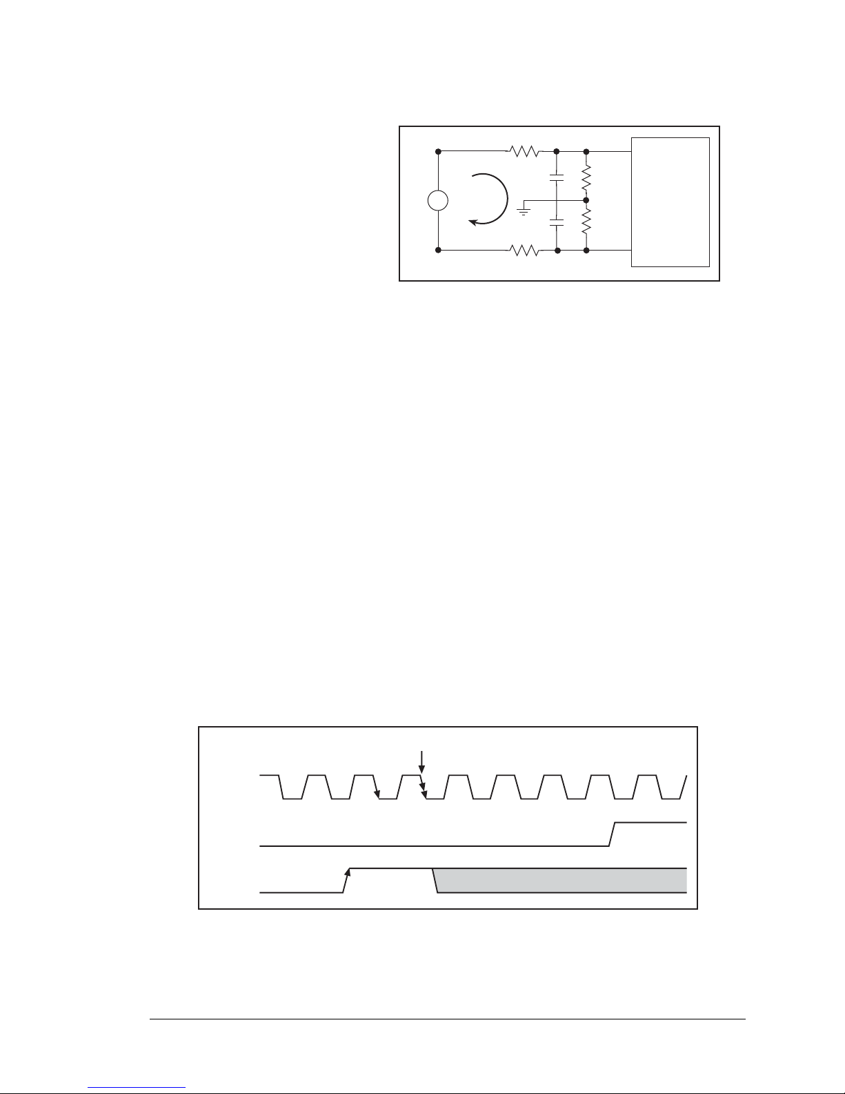
User’s Manual 39
If a device such as a battery is
connected across two channels
for a differential measurement,
and it is not referenced to
analog ground, then the current
from the device will flow
through both sets of attenuator
resistors without flowing back
to analog ground as shown in
Figure 10. This will generate a
negative voltage at one of the
inputs, LN1, which will almost
certainly lead to inaccurate A/D
conversions. T o make such diff erential measurements, connect the R1 resistors to the A/D
converter’s internal reference voltage, which is software-configurable for 1.15 V, 2.048 V,
or 2.5 V. This internal reference voltage is available on pin 49 of header J3 as VREF, and
allows you to convert analog input voltages that are negative with respect to analog ground.
NOTE: The amplifier inside the A/D converter’s internal voltage reference circuit has a
very limited output-current capability. The internal buffer can source up to 20 mA and
sink only up to 200 µA. Use a separate buffer amplifier if you need to supply any load
current.
The A/D converter’s CONVER T pin is available on pin 48 of header J3 and can be used as
a hardware means of forcing the A/D converter to start a conversion cycle at a specific time.
The CONVERT signal is an edge-triggered event and has a hold time of two CCLK periods
for debounce.
A conversion is started by an active (rising) edge on the CONVERT pin. The CONVERT
pin must stay low for at least two CCLK periods before going high for at least two CCLK
periods. Figure 11 shows the timing of a conversion start. The double falling arrow on
CCLK indicates the actual start of the conversion cycle.
Figure 11. Timing Diagram for Conversion Start Using CONVERT Pin
Appendix B.4.3 explains the implementation examples of these features on the Prototyping Board.
Figure 10. Current Flow from Ungrounded
or Floating Source
R5
R6
2.2 nF
R14
R13
2.2 nF
ADC
AIN0
AIN1
+
I
LN0
LN1
+
-
Device
CCLK
BUSY
CONV
Conversion starts
Page 44

40 RabbitCore RCM4100
4.4.1 A/D Converter Power Supply
The analog section is isolated from digital noise generated by other components by way of a
low-pass filter composed of L1, C1, and C2 on the RCM4100 as shown in Figure 12. The
+V analog power supply powers the A/D converter chip.
Figure 12. Analog Supply Circuit
+V
+3.3 V
C1
2.2 nF
C2
100 nF
L1
Page 45

User’s Manual 41
4.5 Other Hardware
4.5.1 Clock Doubler
The clock doubler on the RCM4100 is disabled by default.
4.5.2 Spectrum Spreader
The Rabbit 4000 features a spectrum spreader, which helps to mitigate EMI problems. By
default, the spectrum spreader is on automatically, but it may also be turned off or set to a
stronger setting. The means for doing so is through a simple global macro as shown below.
NOTE: Refer to the Rabbit 4000 Microprocessor User’s Manual for more infor mation
on the spectrum-spreading setting and the maximum clock speed.
1. Select the “Defines” tab from the Dynamic C Options > Project Options menu.
2. Normal spreading is the default, and usually no entry is needed. If you need to specify
normal spreading, add the line
ENABLE_SPREADER=1
For strong spreading, add the line
ENABLE_SPREADER=2
To disable the spectrum spreader, add the line
ENABLE_SPREADER=0
NOTE: The strong spectrum-spreading setting is not recommended since it may limit
the maximum clock speed or the maximum baud rate. It is unlikely that the strong setting will be used in a real application.
3. Click OK to save the macro. The spectrum spreader will now remain of f whenever you
use the project file where you defined the macro.
Page 46

42 RabbitCore RCM4100
4.6 Memory
4.6.1 SRAM
RCM4100 series modules have 256K–512K of data SRAM installed at U10. In addition,
the RCM4100 and RCM4120 have 512K of fast program-execution SRAM installed at U12.
4.6.2 Flash EPROM
All RCM4100 modules also have 512K of flash EPROM installed at U11.
NOTE: Rabbit recommends that any customer applicatio ns should not be constraine d by
the sector size of the flash EPROM since it may be necessary to change the sector size
in the future.
Writing to arbitrary flash memory addresses at run time is discouraged. Instead, define a
“user block” area to store persistent data. The functions writeUserBlock and
readUserBlock are provided for this. Refer to the
Rabbit 4000 Microprocessor
Designer’s Handbook
for additional information.
Page 47

User’s Manual 43
5. SOFTWARE REFERENCE
Dynamic C is an integrated development system for writing
embedded software. It runs on an IBM-compatible PC and is
designed for use with sing le-board computers and other devices
based on the Rabbit microprocessor. Chapter 5 describes the
libraries and function calls related to the RCM4100 series.
5.1 More About Dynamic C
Dynamic C has been in use worldwide since 1989. It is specially designed for programming embedded systems, and features quick compile and interactive debugging. A complete reference guide to Dynamic C is contained in the Dynamic C User’s Manual.
You have a choice of doing your software development in the flash memory or in the static
SRAM included on the RCM4100 series of modules. The flash memory and SRAM
options are selected with the Options > Program Option s > Compiler menu.
The advantage of working in RAM is to save wear on the flash memory, which is limited
to about 100,000 write cycles. The disadvantage is that the code and data might not both
fit in RAM.
NOTE: Do not depend on the flash memory sector size or type in your program logic.
The RCM4100 series of module s an d Dyna mi c C wer e d esi gne d to accommodate flash
devices with various sector sizes in response to the volatility of the flash-memory
market.
Developing software with Dynamic C is simple. Users can write, compile, and test C and
assembly code without leaving the Dynamic C development environment. Debugging
occurs while the application runs on the target. Alternatively, users can compile a program
to an image file for later loading. Dynamic C runs on PCs under Windows 95 and later.
Programs can be downloaded at baud rates of up to 460,800 bps after the program compiles.
Page 48

44 RabbitCore RCM4100
Dynamic C has a number of standard features.
• Full-feature source and/or assembly-level debugger, no in-circuit emulator required.
• Royalty-free TCP/IP stack with source code and most common protocols.
• Hundreds of functions in source-code libraries and sample programs:
X Exceptionally fast support for floating-point arithmetic and transcendental functions.
X RS-232 and RS-485 serial communication.
X Analog and digital I/O drivers.
X I
2
C, SPI, GPS, file system.
X LCD display and keypad drivers.
• Powerful language extensions for cooperative or preemptive multitasking
• Loader utility program to load binary images into Rabbit-based targets in the absence
of Dynamic C.
• Provision for customers to create their own source code libraries and augment on-line
help by creating “function description” block comments using a special format for
library functions.
• Standard debugging features:
X Breakpoints—Set breakpoints that can disable interrupts.
X Single-stepping—Step into or over functions at a source or machine code level, µC/OS-II aware.
X Code disassembly—The disassembly window displays addresses, opcodes, mnemonics, and
machine cycle times. Switch between debugging at machine-code level and source-code level by
simply opening or closing the disassembly window.
X Watch expressions—Watch expressions are compiled when defined, so complex expressions
including function calls may be placed into watch expressions. Watch expressions can be updated
with or without stopping program execution.
X Register window—All processor reg isters and f lags are disp layed. The con tents of gener al regist ers
may be modified in the window by the user.
X Stack window—shows the contents of the top of the stack.
X Hex memory dump—displays the contents of memory at any address.
X STDIO window—
printf outputs to this window and keyboard input on the host PC can be
detected for debugging purposes.
printf output may also be sent to a serial port or file.
Page 49

User’s Manual 45
5.2 Dynamic C Function Calls
5.2.1 Digital I/O
The RCM4100 series of modules was designed to interface with other systems, and so
there are no drivers written spec ifically for the I/O. The genera l Dynamic C re ad and write
functions allow you to customize the parallel I/O to meet your specific needs. For example, use
WrPortI(PEDDR, &PEDDRShadow, 0x00);
to set all the Port E bits as inputs, or use
WrPortI(PEDDR, &PEDDRShadow, 0xFF);
to set all the Port E bits as outputs.
When using the auxiliary I/O bus on the Rabbit 4000 chip, add the line
#define PORTA_AUX_IO // required to enable auxiliary I/O bus
to the beginning of any programs using the auxiliary I/O bus.
The sample programs in the Dynamic C
SAMPLES/RCM4100
folder provide further
examples.
5.2.2 Serial Co mmunication Drive rs
Library files included with Dynamic C provide a full range of serial communications support. The
RS232.LIB
library provides a set of circular-buffer-based serial functions. The
PACKET.LIB
library provides packet-based serial functions where packets can be delimited
by the 9th bit, by transmission gaps, or with user-defined special characters. Both libraries
provide blocking functions, which do not return until they are finished transmitting or
receiving, and nonblocking functions, which must be called repeatedly until they are finished, allowing other functions to be performed between calls. For more information, see
the Dynamic C Function Reference Manual and Technical Note TN213, Rabbit Serial
Port Software.
5.2.3 SRAM Use
The RCM4100 series of modules has a battery-backed data SRAM and a program-execution SRAM. Dynamic C provides the
protected
keyword to identify variables that are to
be placed into the battery-backed SRAM. The compiler generates code that maintains two
copies of each protected variable in the battery-backed SRAM. The comp iler also generate s
a flag to ind icat e whic h copy of the protected variable is valid at the current time. This flag
is also stored in the battery-backed SRAM. When a protected variable is updated, the
“inactive” copy is modified, and is made “active” only when the update is 100% complete.
This assures the integrity of the data in case a reset or a power failure occurs during the
update process. At power-on the application program uses the active copy of the variable
pointed to by its associated flag.
Page 50

46 RabbitCore RCM4100
The sample code below shows how a protected variable is defined and how its value can
be restored.
main() {
protected int state1, state2, state3;
...
_sysIsSoftReset(); // restore any protected variables
Additional information on
protected
variables is available in the Dynamic C User’s
Manual.
Page 51

User’s Manual 47
5.2.4 Prototyping Board Function Calls
The functions described in this section are for use with the Prototyping Board features.
The source code is in the Dynamic C
LIB\Rabbit4000\RCM4xxx\RCM41xx.LIB
library if you need to modify it for your own board design.
NOTE: The analog input fun ction c alls are supp orted o nly by the RCM4 100 model s ince
the RCM4110 and the RCM4120 do not have an A/D converter.
The sample programs in the Dynamic C
SAMPLES\RCM4100
folder illustrate the use of
the function calls.
Other generic functions applicable to all devices based on Rabbit microprocessors are
described in the Dynamic C Function Reference Manual.
5.2.4.1 Board Initialization
brdInit
void brdInit(void);
DESCRIPTION
Call this function at the beginning of your program. This function initializes Parallel
Ports A through E for use with the Prototyping Board, and on the RCM4100 model
loads the stored calibration constants for the A/D converter . This function call is intended
for demonstration purposes only, and can be modified for your applications.
Summary of Initialization
1. I/O port pins are configured for Prototyping Board operation.
2. Unused configurable I/O are set as tied outputs.
3. RS-232 is not enabled.
4. LEDs are off.
5. The slave port is disabled.
RETURN VALUE
None.
Page 52

48 RabbitCore RCM4100
5.2.4.2 Alerts
These function calls can be found in the Dynamic C LIB\Rabbit4000\RCM4xxx\
RCM4xxx.LIB
library.
timedAlert
void timedAlert(unsigned long timeout);
DESCRIPTION
Polls the real-time clock until a timeout occurs. The RCM4100 series of RabbitCore
modules will be in a low-power mode during this time. Once the timeout occurs, this
function call will enable the normal power source.
PARAMETER
timeout the duration of the timeout in seconds
RETURN VALUE
None.
digInAlert
void digInAlert(int dataport, int portbit, int value,
unsigned long timeout);
DESCRIPTION
Polls a digital input for a set value or until a timeout occurs. The RCM4400W will be
in a low-power mode during this time. Once a timeout occurs or the correct byte is
received, this function call will enable the normal po wer source and exit.
PARAMETERS
dataport the input port data register to poll (e.g., PADR)
portbit the input port bit (0–7) to poll
value the value of 0 or 1 to receive
timeout
the duration of the timeout in seconds (enter 0 for no timeout)
RETURN VALUE
None.
Page 53

User’s Manual 49
5.2.5 Analog Inputs (RCM4100 only)
The function calls used with the Prototyping Board features and the A/D converter on the
RCM4100 model are in the Dynamic C LIB\Rabbit4000\RCM4xxx\ADC_ADS7870.LIB
library. Dynamic C v. 10.07 or later is required to use the A/D converter function calls.
anaInConfig
unsigned int anaInConfig(unsigned int instructionbyte,
unsigned int cmd, long brate);
DESCRIPTION
Use this function to configure the A/D converter. This function will address the A/D
converter chip in Register Mode only, and will return an error if you try the Direct
Mode. Appendix B.4.3 provides additional addressing and command information.
ADS7870 Signal ADS7870 State RCM4100 Function/State
LN0 Input AIN0
LN1 Input AIN1
LN2 Input AIN2
LN3 Input AIN3
LN4 Input AIN4
LN5 Input AIN5
LN6 Input AIN6
LN7 Input AIN7
/RESET Input Board reset device
RISE/FALL Input Pulled up for SCLK active on rising edge
I/O0 Input Pulled down
I/O1 Input Pulled down
I/O2 Input Pulled down
I/O3 Input Pulled down
CONVERT Input Pulled down when not driven
BUSY Output PE0 pulled down; logic high state converter is busy
CCLKCNTRL Input Pulled down; 0 state sets CCLK as input
CCLK Input Pulled down; external conversion clock
SCLK Input PB0; serial data transfer clock
SDI Input PC4; 3-wire mode for serial data input
SDO Output PC5; serial data output /CS driven
/CS Input BUFEN pulled up; active-low enables serial interface
BUFIN Input Driven by VREF
VREF Output Connected to BUFIN and BUFOUT
BUFOUT Output Driven by VREF
Page 54

50 RabbitCore RCM4100
anaInConfig (continued)
PARAMETERS
instructionbyte
the instruction byte that will initiat e a read or write operation
at 8 or 16 bits on the designated register addres s. For example,
checkid = anaInConfig(0x5F, 0, 9600);
// read ID and set baud rate
cmd
the command data that configure the registers addressed by the instruction byte . Enter 0 i f you are p erfo rming a rea d oper ati on. For
example,
i = anaInConfig(0x07, 0x3b, 0);
// write ref/osc reg and enable
brate
the serial cl ock t rans fer rate of 9600 to 1 1 5,20 0 byt es p er s econd.
brate
must be set the first time this function is called. Enter 0 for
this parameter thereafter, for exampl e,
anaInConfig(0x00, 0x00, 9600);
// resets device and sets byte rate
RETURN VALUE
0 on write operations
data value on read operations
SEE ALSO
anaInDriver, anaIn, brdInit
Page 55

User’s Manual 51
anaInDriver
int anaInDriver(unsigned int cmd);
DESCRIPTION
Reads the voltage of an analog input channel by serial-clocking an 8-bit command to
the A/D converter by its Direct Mode method. This fun ction assumes that Mode1 (mos t
significant byte first) and the A/D convert er oscill ator have been en abled. See
anaIn-
Config()
for the setup.
The conversion begins immediately after the last data bit has been transferred. An exception error will occur if Direct Mode bit D7 is not set.
PARAMETERS
cmd contains a gain code and a channel code as follows.
D7—1; D6–D4—Gain Code; D3–D0—Channel Code
Use the following calculation and the tables below to determine cmd:
cmd = 0x80 | (gain_code*16) + channel_code
Gain Code
Gain
Multiplier
0×1
1×2
2×4
3×5
4×8
5×10
6×16
7×20
Page 56

52 RabbitCore RCM4100
anaInDriver (continued)
RETURN VALUE
A value corresponding to the voltage on the analog input channel:
0–2047 for 11-bit conversions
-2048–2047 for 12-bi t con versions
ADTIMEOUT
(-4095) if the conversion is incomplete or busy bit timeout
ADOVERFLOW
(-4096) for overflow or out of range
SEE ALSO
anaInConfig, anaIn, brdInit
Channel Code
Differential Input
Lines
Channel Code
Single-Ended
Input Lines
*
* Negative input is ground.
4–20 mA
Lines
0 +AIN0 -AIN1 8 AIN0 AIN0*
1 +AIN2 -AIN3 9 AIN1 AIN1*
2 +AIN4 -AIN5 10 AIN2 AIN2*
3
†
† Not accessible on Prototyping Board
+AIN6 -AIN7 11 AIN3 AIN3
4 -AIN0 +AIN1 12 AIN4 AIN4
5 -AIN2 +AIN3 13 AIN5 AIN5
6 -AIN4 +AIN5 14 AIN6 AIN6
7
‡
‡ Not accessible on Prototyping Board
-AIN6 +AIN7 15 AIN7 AIN7*
Page 57

User’s Manual 53
anaIn
int anaIn(unsigned int channel, int opmode, int gaincode);
DESCRIPTION
Reads the value of an analog i nput channel using the Direct Mode method of a ddressing
the A/D converter. Note that it takes about 1 second to ensure an internal capacitor on
the A/D conve rter is charged when the function is called th e first time.
PARAMETERS
channel
the channel number (0 to 7) corresponding to LN0 to LN7.
opmode
the mode of operation:
SINGLE
—single-ended input
DIFF
—differential input
mAMP
—4–20 mA input
gaincode the gain code of 0 to 7 (applies only to Prototyping Board):
channel SINGLE DIFF mAMP
0 +AIN0 +AIN0 -AIN1
+AIN0
*
* Not accessible on Prototyping Board.
1 +AIN1 +AIN1 -AIN0* +AIN1*
2 +AIN2 +AIN2 -AIN3 +AIN2*
3 +AIN3 +AIN3 -AIN2* +AIN3
4 +AIN4 +AIN4 -AIN5 +AIN4
5 +AIN5 +AIN5 -AIN4* +AIN5
6 +AIN6 +AIN6 -AIN7* +AIN6
7 +AIN7 +AIN7 -AIN6* +AIN7*
Gain Code
Gain
Multiplier
Voltage Range
*
(V)
* Applies to Prototyping Board.
0 ×1 0–22.5
1 ×2 0–11.25
2×40–5.6
3×50–4.5
4×80–2.8
5 ×10 0–2.25
6 ×16 0–1.41
7 ×20 0–1.126
Page 58

54 RabbitCore RCM4100
anaIn (continued)
RETURN VALUE
A value corresponding to the voltage on the analog input channel:
0–2047 for single-ended conversions
-2048–2047 for differential conversions
ADTIMEOUT
(-4095) if the conversion is incomplete or busy bit timeout
ADOVERFLOW
(-4096) for overflow or out of range
SEE ALSO
anaIn, anaInConfig, anaInDriver
Page 59

User’s Manual 55
anaInCalib
int anaInCalib(int channel, int opmode, int gaincode,
int value1, float volts1, int value2, float volts2);
DESCRIPTION
Calibrates the re spons e of the des ired A/D co nverter cha nnel as a l inear f unction using
the two conversion points provided. Four values are calculated and placed into global
tables
_adcCalibS, _adcCalibD
, and
adcCalibM
to be later st ored in to si mulat-
ed EEPROM using the funct i on
anaInEEWr()
. Each channel will have a li ne ar con-
stant and a voltage offset.
PARAMETERS
channel the channel number (0 to 7) corresponding to LN0 to LN7.
opmode
the mode of operation:
SINGLE
—single-ended input
DIFF
—differential input
mAMP
—4–20 mA input
channel SINGLE DIFF mAMP
0 +AIN0 +AIN0 -AIN1
+AIN0
*
* Not accessible on Prototyping Board.
1 +AIN1 +AIN1 -AIN0* +AIN1*
2 +AIN2 +AIN2 -AIN3 +AIN2*
3 +AIN3 +AIN3 -AIN2* +AIN3
4 +AIN4 +AIN4 -AIN5 +AIN4
5 +AIN5 +AIN5 -AIN4* +AIN5
6 +AIN6 +AIN6 -AIN7* +AIN6
7 +AIN7 +AIN7 -AIN6* +AIN7*
Page 60
56 RabbitCore RCM4100
anaInCalib (continued)
gaincode the gain code of 0 to 7 (applies only to Prototyping Board):
value1 the first A/D converter channel raw count value (0–2047)
volts1 the voltage or current corresponding to the first A/D converter
channel value (0 to +20 V or 4 to 20 mA)
value2 the second A/D converter channel raw count value (0–2047)
volts2 the voltage or current corresponding to the first A/D converter
channel value (0 to +20 V or 4 to 20 mA)
RETURN VALUE
0 if successful.
-1 if not able to make calibration constants.
SEE ALSO
anaIn, anaInVolts, anaInmAmps, anaInDiff, anaInCalib, brdInit
Gain Code
Gain
Multiplier
Voltage Range
*
(V)
* Applies to Prototyping Board.
0 ×1 0–22.5
1 ×2 0–11.25
2×40–5.6
3×50–4.5
4×80–2.8
5 ×10 0–2.25
6 ×16 0–1.41
7 ×20 0–1.126
Page 61
User’s Manual 57
anaInVolts
float anaInVolts(unsigned int channel, unsigned int gaincode);
DESCRIPTION
Reads the state of a single-ended analog input channel and uses the previously set
calibration constants to convert it to volts.
PARAMETERS
channel the channel number (0 to 7) corresponding to LN0 to LN7.
gaincode the gain code of 0 to 7 (applies only to Prototyping Board):
Channel Code
Single-Ended
Input Lines
*
* Negative input is ground.
Voltage Range
†
(V)
† Applies to Prototyping Board.
0 +AIN0 0–22.5
1 +AIN1 0–22.5
2 +AIN2 0–22.5
3 +AIN3 0–22.5
4 +AIN4 0–22.5
5 +AIN5 0–22.5
6 +AIN6 0–22.5
7+AIN7
0–2
‡
‡ Used for thermistor in sample program.
Gain Code
Gain
Multiplier
Voltage Range
*
(V)
* Applies to Prototyping Board.
0 ×1 0–22.5
1 ×2 0–11.25
2×40–5.6
3×50–4.5
4×80–2.8
5 ×10 0–2.25
6 ×16 0–1.41
7 ×20 0–1.126
Page 62

58 RabbitCore RCM4100
anaInVolts (continued)
RETURN VALUE
A voltage value corresponding to the voltage on the analog input channel.
ADTIMEOUT
(-4095) if the conversion is incomplete or busy bit timeout.
ADOVERFLOW
(-4096) for overflow or out of range.
SEE ALSO
anaInCalib, anaIn, anaInmAmps, brdInit
Page 63
User’s Manual 59
anaInDiff
float anaInDiff(unsigned int channel, unsigned int gaincode);
DESCRIPTION
Reads the state o f diff erential analog input channels an d uses the previousl y set calibr ation constants to convert it to vo lts.
PARAMETERS
channel the channel number (0 to 7) corresponding to LN0 to LN7.
gaincode the gain code of 0 to 7 (applies only to Prototyping Board):
channel DIFF
Voltage Range
(V)
0+AIN0 -AIN1
-22.5 to +22.5
*
* Accessible on Prototyping Board.
1+AIN1 -AIN1 —
2 +AIN2 -AIN3 -22.5 to +22.5*
3+AIN3 -AIN3 —
4 +AIN4 -AIN5 -22.5 to +22.5*
5+AIN5 -AIN5 —
6+AIN6 -AIN7 —
7+AIN7 -AIN7 —
Gain Code
Gain
Multiplier
Voltage Range
*
(V)
* Applies to Prototyping Board.
0 ×1 -22.5 – +22.5
1 ×2 -1 1. 25 – +11.25
2 ×4 -5.6 – +5.6
3 ×5 -4.5 – +4.5
4 ×8 -2.8 – +2.8
5 ×10 -2.25 – +2.25
6 ×16 -1.41 – +1.41
7 ×20 -1.126 – +1.126
Page 64

60 RabbitCore RCM4100
anaInDiff (continued)
RETURN VALUE
A voltage value corresponding to the voltage differential on the analog input channel.
ADTIMEOUT
(-4095) if the conversion is incomplete or busy bit timeout.
ADOVERFLOW
(-4096) for overflow or out of range.
SEE ALSO
anaInCalib, anaIn, anaInmAmps, brdInit
Page 65

User’s Manual 61
anaInmAmps
float anaInmAmps(unsigned int channel);
DESCRIPTION
Reads the state of an analog input channel and uses the previously set calibration constants to convert it to current.
PARAMETERS
channel the channel number (0 to 7) corresponding to LN0 to LN7.
RETURN VALUE
A current value between 4. 00 and 20.00 mA corresp onding to the curre nt on the a nalog
input channel.
ADTIMEOUT
(-4095) if the conversion is incomplete or busy bit timeout.
ADOVERFLOW
(-4096) for overflow or out of range.
SEE ALSO
anaInCalib, anaIn, anaInVolts
Channel Code
4–20 mA
Input Lines
*
* Negative input is ground.
0+AIN0
1+AIN1
2+AIN2
3
+AIN3
†
† Applies to Prototyping Board.
4 +AIN4*
5 +AIN5*
6 +AIN6*
7+AIN7
Page 66

62 RabbitCore RCM4100
anaInEERd
root int anaInEERd(unsigned int channel, unsigned int opmode,
unsigned int gaincode);
DESCRIPTION
Reads the cali br at ion constants, gai n, and offs et for an input ba se d on their desig na te d
position in the flash memory, and places them into global tables
_adcCalibS
,
_adcCalibD
, and
_adcCalibM
for analog inputs. Dependi ng on th e flas h siz e, the
following macros can be used to identify the starting address for these locations.
ADC_CALIB_ADDRS, address start of single-ended analog input channels
ADC_CALIB_ADDRD, address start of differential analog input channels
ADC_CALIB_ADDRM, address start of milliamp analog input channels
NOTE: This function cannot be run in RAM.
PARAMETER
channel the channel number (0 to 7) corresponding to LN0 to LN7.
opmode
the mode of operation:
SINGLE
—single-ended input
DIFF
—differential input
mAMP
—4–20 mA input
channel SINGLE DIFF mAMP
0 + AIN0 +AIN0 -AIN1
+AIN0
*
* Not accessible on Proto typing Board.
1 + AIN1 +AIN1 -AIN0* +AIN1*
2 + AIN2 +AIN2 -AIN3 +AIN2*
3 + AIN3 +AIN3 -AIN2* +AIN3
4 + AIN4 +AIN4 -AIN5 +AIN4
5 + AIN5 +AIN5 -AIN4* +AIN5
6 + AIN6 +AIN6 -AIN7* +AIN6
7 + AIN7 +AIN7 -AIN6* +AIN7*
ALLCHAN read all channels for selected opmode
Page 67

User’s Manual 63
anaInEERd (continued)
gaincode the gain code of 0 to 7. The gaincode parameter is ignored when
channel is ALLCHAN.
RETURN VALUE
0 if successful.
-1 if address is invalid or out of range.
SEE ALSO
anaInEEWr, anaInCalib
Gain Code
Gain
Multiplier
Voltage Range
*
(V)
* Applies to Prototyping Board.
0
×1 0–22.5
1
×2 0–11.25
2 ×4 0–5.6
3 ×5 0–4.5
4
×8 0–2.8
5
×10 0–2.25
6
×16 0–1.41
7
×20 0–1.126
Page 68

64 RabbitCore RCM4100
anaInEEWr
int anaInEEWr(unsigned int channel, int opmode,
unsigned int gaincode);
DESCRIPTION
Writes the calibration constants, ga in, and offset for an in put based from global tables
_adcCalibS, _adcCalibD
, and
_adcCalibM
to designated pos itions in the flash
memory . Depe nding on th e flash si ze, the fo llowing macros can be used to ide ntify the
starting address for these locations.
ADC_CALIB_ADDRS, address start of single-ended analog input channels
ADC_CALIB_ADDRD, address start of differential analog input channels
ADC_CALIB_ADDRM, address start of milliamp analog input channels
NOTE: This function cannot be run in RAM.
PARAMETER
channel the channel number (0 to 7) corresponding to LN0 to LN7.
opmode
the mode of operation:
SINGLE
—single-ended input
DIFF
—differential input
mAMP
—4–20 mA input
channel SINGLE DIFF mAMP
0 +AIN0 +AIN0 -AIN1
+AIN0
*
* Not accessible on Prototyping Board.
1 +AIN1 +AIN1 -AIN0* +AIN1*
2 +AIN2 +AIN2 -AIN3 +AIN2*
3 +AIN3 +AIN3 -AIN2* +AIN3
4 +AIN4 +AIN4 -AIN5 +AIN4
5 +AIN5 +AIN5 -AIN4* +AIN5
6 +AIN6 +AIN6 -AIN7* +AIN6
7 +AIN7 +AIN7 -AIN6* +AIN7*
ALLCHAN read all channels for selected opmode
Page 69

User’s Manual 65
anaInEEWr (continued)
gaincode the gain code of 0 to 7. The gaincode parameter is ignored when
channel is ALLCHAN.
RETURN VALUE
0 if successful
-1 if address is invalid or out of range.
SEE ALSO
anaInEEWr, anaInCalib
Gain Code
Gain
Multiplier
Voltage Range
*
(V)
* Applies to Prototyping Board.
0 ×1 0–22.5
1 ×2 0–11.25
2×40–5.6
3×50–4.5
4×80–2.8
5 ×10 0–2.25
6 ×16 0–1.41
7 ×20 0–1.126
Page 70

66 RabbitCore RCM4100
5.3 Upgrading Dynamic C
Dynamic C patches that focus on bug fixes are available from time to time. C heck the Web
site www.rabbit.com/support/ for the latest patches, workarounds, and bug fixes.
5.3.1 Add-On Modules
Starting with Dynamic C version 10.40, Dynamic C includes the popular µC/OS-II realtime operating system, point-to-point protocol (PPP), FAT file system, RabbitWeb, and
other select libraries. Rabbit also offers for purchase the Rabbit Embedded Security Pack
featuring the Secure Sockets Layer (SSL) and a specific Advanced Encryption Standard
(AES) library.
In addition to the Web-based technical support included at no extra charge, a one-year
telephone-based technical support subscription is also available for purchase.
V isit o ur Web site at www.rabbit.com for further information and complete docum entation.
Page 71

User’s Manual 67
APPENDIX A. RCM4100 SPECIFICATIONS
Appendix A provides the specifications for the RCM4100 series
of modules, and describes the conformal coating.
Page 72

68 RabbitCore RCM4100
A.1 Electrical and Mechanical Characteristics
Figure A-1 shows the mechanical dimensions for the RCM4100 series of modules.
Figure A-1. RCM4100 Dimensions
NOTE: All measurements are in inc hes fo llowed b y milli meters enclos ed in pa renthe ses.
All dimensions have a manufacturing tolerance of ±0.01" (0.25 mm).
Please refer to the RCM4100
footprint diagram later in this
appendix for precise header
locations.
× 2
0.125
dia
(3.2)
R1
J1
R2
R5
R4
R3
JP1
JP2
JP9
JP6
JP7
JP3
JP5
JP4
C4
C3
C2
L1
C1
R7
R8
R6
R10
R9
U1
U2
R11
C15
RP2
C16
C17
D1
R27
RP1
R15
C23
R17
R16
C21
C14
U6
R19
R18
R22
R23
Y2
C27
U7
C28
R21
JP8
JP10
JP11
JP12
C5
Y1
Q1
C6
C7
C8
C9
C10 C11
U5
C12
C13
R12
C24
R14
C25
C26
C19
C20
U4
U3
C18
R13
C30
C31
C34 C35
C32
C33
C29
C38
C39
C37
C36
J2
0.72
(18)
1.41
(36)
0.20
(5)
0.11
(2.8)
0.23
(5.8)
1.88
(48)
0.91
(23)
0.19
(5)
0.50
(13)
0.78
(20)
0.19
(5)
1.41
(36)
0.49
(12)
0.20
(5)
0.11
(2.8)
0.23
(5.8)
0.49
(12)
1.88
(48)
0.064
(1.6)
0.064
(1.6)
Page 73

User’s Manual 69
It is recommended that you allow for an “exclusion zone” of 0.04" (1 mm) around the
RCM4100 modules in all directions when the RCM4100 is incorporated into an assembly
that includes other printed circuit boards. An “exclusion zone” of 0.08" (2 mm) is recommended below the RCM4100 module when the RCM4100 is plugged into another assembly. Figure A-2 shows this “exclusion zone.”
Figure A-2. RCM4100 “Exclusion Zone”
J2
Exclusion
Zone
1.850
(47.0)
0.24
(6)
1.96
(50)
1.93
(49.0)
0.08
(2)
0.08
(2)
1.88
(48)
0.24
(6)
Page 74
70 RabbitCore RCM4100
T ableA-1 lists the electrical, mechanical, and environmental specifications for the RCM4100
series of modules.
Table A-1. RCM4100 Specifications
Parameter RCM4100 RCM4110 RCM4120
Microprocessor
Rabbit
®
4000
at 58.98 MHz
Rabbit® 4000
at 29.49 MHz
Rabbit® 4000
at 58.98 MHz
Flash Memory 512K
Data SRAM 512K 256K 512K
Fast Program-Execution
SRAM
512K — 512K
Backup Battery
Connection for user-supplied backup battery
(to support RTC and data SRAM)
General Purpose I/O
29 parallel digital I/0
lines:
• configurable with
four layers of
alternate functions
40 parallel digital I/0 lines:
• configurable with four layers of alternate
functions
Additional Inputs
Startup mode (2),
reset in, CONVERT
Startup mode (2), reset in
Additional Outputs
Status, reset out,
analog VREF
Status, rese t out
Analog Inputs
8 channels single-ended
or 4 channels dif ferential
Programm able gain
1, 2, 4, 5, 8, 10, 16, and
20 V/V
——
• A /D Converter
Resolution
12 bits (11 bits single-
ended)
• A /D Conversion Time
(including 120 µs raw
count and Dynamic C)
180 µs
Auxiliary I/O Bus
Can be configured for 8 data lines and
6 address lines (shared with parallel I/O lines), plus I/O read/write
Page 75
User’s Manual 71
Serial Ports
6 high-speed, CMOScompatible ports:
• all 6 configurable as
asynchronous (with
IrDA), 4 as clocked
serial (SPI), and 2 as
SDLC/HDLC
• 1 asynchronous
clocked serial port
shared with programming port
• 1 clocked serial port
shared with A/D converter
6 high-speed, CMOS-compatible ports:
• all 6 configurable as asynchronous (with IrDA),
4 as clocked serial (SPI), and 2 as SDLC/HDLC
• 1 asynchronous clocked serial port shar ed wit h
programming port
Serial Rate Maximum asynchronous baud rate = CLK/8
Slave Interface
Slave port allows the RCM4100 to be used as an intelligent peripheral device
slaved to a master processor
Real Time Clock Yes
Timers
Ten 8-bit timers (6 cascadable from the first),
one 10-bit timer with 2 match registers, and
one 16-bit timer with 4 ou tputs and 8 set /reset registers
W atchdog/Supervisor Yes
Pulse-Wi dth Modulators
4 channels synchronized PWM with 10-bit counter
4 channels variable-phase or synchronized PWM with 16-bit counter
Input Capture
2-channel input capture can be used to time input signals
from various port pins
Quadrature Decoder
2-channel quadrature decoder accepts inputs
from external incremental encoder modules
Power
(pins unloaded)
3.0– 3.6 V.DC
125 mA @ 3.3 V 65 mA @ 3.3 V 125 mA @ 3.3 V
Operating Temperature -40°C to +85°C 0°C to +70°C -40°C to +85°C
Humidity 5% to 95%, noncondensing
Connectors
One 2 × 25, 1.27 mm pitch IDC signal header
One 2 × 5, 1.27 mm pitch IDC programming header
Board Size
1.41" × 1.88" × 0.49"
(36 mm × 48 mm × 12 mm)
Table A-1. RCM4100 Specifications (continued)
Parameter RCM4100 RCM4110 RCM4120
Page 76

72 RabbitCore RCM4100
A.1.1 A/D Converter
Table A-2 shows some of the important A/D converter specifications. For more details,
refer to the ADC7870 data sheet.
Table A-2. A/D Converter Specifications
Parameter Test Conditions Typ Max
Analog Input Characteristics
Input Capa citance
Input Impedance
Common-Mode
Differential Mode
4 – 9.7 pF
6 MΩ
7 MΩ
Static Accuracy
Resolution
Single-Ended Mode
Differential Mode
Integral Linearity
Differential Linearity
11 bits
12 bits
±1 LSB
±0.5 LSB
±2.5 LSB
Dynamic Characteristics
Throughput Rate 52 ksamples/s
Voltage Reference
Accuracy
Buffer Amp Source Current
Buffer Amp Sink Current
Short-Circuit Current
V
ref
= 2.048 V and 2.5 V
±0.05%
20 mA
200 µA
20 mA
±0.25%
Page 77
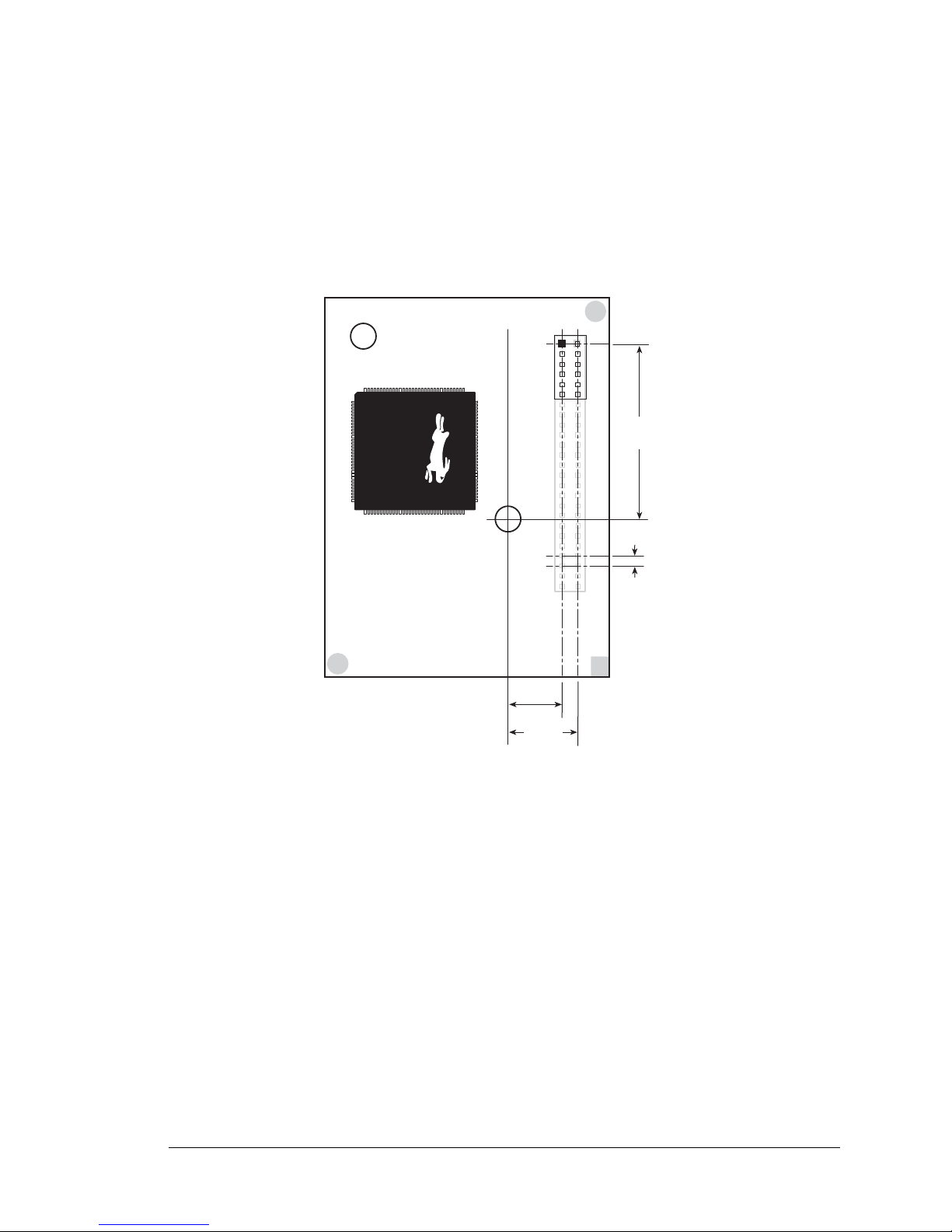
User’s Manual 73
A.1.2 Headers
The RCM4100 series uses a header at J2 for physical connection to other boards. J2 is a
2 × 25 SMT header with a 1.27 mm pin spacing. J1, the programming port, is a 2 × 5
header with a 1.27 mm pin spacing.
Figure A-3 shows the layout of another board for the RCM4100 to be plugged into. These
reference design values are relative to one of the mounting holes.
Figure A-3. User Board Footprint for RCM4100 Series
J2
RCM4100 Series
Footprint
J1
0.050
(1.27)
0.284
(7.2)
0.334
(8.5)
0.875
(22.2)
Page 78
74 RabbitCore RCM4100
A.2 Rabbit 4000 DC Characteristics
Stresses beyond those listed in Table A-3 may cause permanent damage. The ratings are
stress ratings only, and functional operation of the Rabbit 4000 chip at these or any other
conditions beyond those indicated in this section is not implied. Exposure to the absolute
maximum rating conditions for extended periods may affect the reliability of the Rabbit
4000 chip.
Table A-4 outlines the DC characteristics for the Rabbit 4000 at 3.3 V over the recommended operating temperature range from T
A
= –40°C to +85°C, VDDIO = 3.0 V to 3.6 V.
Table A-3. Rabbit 4000 Absolute Maximum Ratings
Symbol Parameter Maximum Rating
T
A
Operating Temperature -40° to +85°C
T
S
Storage Temperature -55° to +125°C
V
IH
Maximum Input Voltage
VDD
IO
+ 0.3 V
(max. 3.6 V)
VDD
IO
Maximum Operating Voltage 3.6 V
Table A-4. 3.3 Volt DC Characteristics
Symbol Parameter Min Typ Max
VDD
IO
I/O Ring Supply Voltage, 3.3 V 3 .0 V 3.3 V 3.6 V
I/O Ring Supply Voltage, 1.8 V 1.65 V 1.8 V 1.90 V
V
IH
High-Level Input Voltage
(VDD
IO
= 3.3 V)
2.0 V
V
IL
Low-Level Input Voltage
(VDD
IO
= 3.3 V)
0.8 V
V
OH
High-Level Output Voltage
(VDD
IO
= 3.3 V)
2.4 V
V
OL
Low-Level Output Voltage
(VDD
IO
= 3.3 V)
0.4 V
I
IO
I/O Ring Current @ 29.4912 MHz,
3.3 V, 25°C
12.2 mA
I
DRIVE
All other I/O
(except TXD+, TXDD+, TXD-, TXDD-)
8 mA
Page 79
User’s Manual 75
A.3 I/O Buffer Sourcing and Sinking Limit
Unless otherwise specified, the Rabbit I/O buffers are capable of sourcing and sinking
8 mA of current per pin at full AC switching speed. Full AC switching assumes a
29.4 MHz CPU clock with the clock doubler enabled and capacitive loading on address
and data lines of less than 70 pF per pin. The absolute maximum operating voltage on all
I/O is 3.6 V.
A.4 Bus Loading
You must pay careful attention to bus loading when designing an interface to the
RCM4100 series of modules. This section provides bus loading information for external
devices.
Table A-5 lists the capacitance for the various RCM4100 I/O ports.
Table A-6 lists the external capacitive bus loading for the various RCM4100 series output
ports. Be sure to add the loads for the devices you are using in your custom system and
verify that they do not exceed the values in Table A-6.
Table A-5. Capacitance of Rabbit 4000 I/O Ports
I/O Ports
Input
Capacitance
(pF)
Output
Capacitance
(pF)
Parallel Ports A to E 12 14
Table A-6. External Capacitive Bus Loading -40°C to +85°C
Output Port
Clock Speed
(MHz)
Maximum External
Capacitive Loading (pF)
All I/O lines with clock
doubler enabled
58.98 100
Page 80

76 RabbitCore RCM4100
Figure A-4 shows a typical timing diagram for the Rabbit 4000 microprocessor external
I/O read and write cycles.
Figure A-4. External I/O Read and Write Cycles—No Extra Wait States
NOTE: /IOCSx can be programmed to be active low (default) or active high.
T
adr
T
adr
External I/O Read (no extra wait states)
CLK
A[15:0]
External I/O Write (no extra wait states)
CLK
A[15:0]
/IORD
valid
T1
Tw
T1
Tw
T2
valid
T2
/BUFEN
/IOCSx
/IOWR
/BUFEN
D[7:0]
valid
T
setup
T
hold
/CSx
/IOCSx
T
CSx
T
IOCSx
T
IORD
T
BUFEN
T
CSx
T
IOCSx
T
IORD
T
BUFEN
valid
D[7:0]
/CSx
T
CSx
T
IOCSx
T
IOWR
T
CSx
T
IOCSx
T
IOWR
T
BUFEN
T
BUFEN
T
DHZV
T
DVHZ
Page 81

User’s Manual 77
Table A-7 lists the delays in gross memory access time for several values of VDDIO.
The measurements are taken at the 50% points under the following conditions.
• T = -40°C to 85°C, V = VDD
IO
±10%
• Internal clock to nonloaded CLK pin delay ≤ 1 ns @ 85°C/3.0 V
The clock to address output delays are similar, and apply to the following delays.
• T
adr
, the clock to address delay
• T
CSx
, the clock to memory chip select delay
• T
IOCSx
, the clock to I/O chip select delay
• T
IORD
, the clock to I/O read strobe delay
• T
IOWR
, the clock to I/O write strobe delay
• T
BUFEN
, the clock to I/O buffer enable delay
The data setup time delays are similar for both T
setup
and T
hold
.
When the spectrum spreader is enabled with the clock doubler, every other clock cycle is
shortened (sometimes lengthened) by a maximum amount given in the table above. The
shortening takes place by shortening the high part of the clock. If the doubler is not
enabled, then every clock is shortened during the low part of the clock period. The maximum shortening for a pair of clocks combined is shown in the table.
Technical Note TN227, Interfacing External I/O with Rabbit Microprocessor Designs,
contains suggestions for interfacing I/O devices to the Rabbit 4000 microprocessors.
Table A-7. Preliminary Data and Clock Delays
VDD
IO
(V)
Clock to Address
Output Delay
(ns)
Data Setup
Time Delay
(ns)
Worst-Case
Spectrum Spreader Delay
(ns)
30 pF 60 pF 90 pF
0.5 ns setting
no dbl / dbl
1 ns setting
no dbl / dbl
2 ns setting
no dbl / dbl
3.3 6 8 11 1 2.3 / 2.3 3 / 4.5 4.5 / 9
1.8 18 24 33 3 7 / 6.5 8 / 12 11 / 22
Page 82

78 RabbitCore RCM4100
A.5 Jumper Configurations
Figure A-5 shows the header locations used to configure the various RCM4100 options
via jumpers.
Figure A-5. Location of RCM4100 Configurable Positions
Table A-8 lists the configuration options.
Table A-8. RCM4100 Jumper Configurations
Header Description Pins Connected
Factory
Default
JP1 LN0 or PD0 on J2 pin 40
1–2 LN0 RCM4100
2–3 PD0 RCM4110
JP2 LN2 or PD2 on J2 pin 42
1–2 LN2 RCM4100
2–3 PD2 RCM4110
JP3 LN6 or PD6 on J2 pin 46
1–2 LN6 RCM4100
2–3 PD6 RCM4110
JP4 LN7 or PD7 on J2 pin 47
1–2 LN7 RCM4100
2–3 PD7 RCM4110
JP5 LN5 or PD5 on J2 pin 45
1–2 LN5 RCM4100
2–3 PD5 RCM4110
JP6 LN4 or PD4 on J2 pin 44
1–2 LN4 RCM4100
2–3 PD4 RCM4110
JP7 LN3 or PD3 on J2 pin 43
1–2 LN3 RCM4100
2–3 PD3 RCM4110
JP1
JP2
JP9
JP6
JP7
JP3
JP5
JP4
JP12
JP11
JP10
JP8
Top Side
RCM4100
Page 83

User’s Manual 79
NOTE: The jumper connections are made using 0 Ω surface-mounted resistors.
JP8 Data SRAM Size
1–2 512K
2–3 256K
×
JP9 LN1 or PD1 on J2 pin 41
1–2 LN1 RCM4100
2–3 PD1 RCM4110
JP10 PE5 or SMODE0 Output on J2
1–2 PE5
×
2–3 SMODE0
JP11 PE6 or SMODE1 Output on J2
1–2 PE6
×
2–3 SMODE1
JP12 PE7 or STATU S Output on J2
1–2 PE7
×
2–3 STATUS
Table A-8. RCM4100 Jumper Configurations
Header Description Pins Connected
Factory
Default
Page 84

80 RabbitCore RCM4100
A.6 Conformal Coating
The areas around the 32 kHz real-time clock crystal oscillator have had the Dow Corning
silicone-based 1-2620 conformal coating applied. The conformally coated area is shown
in Figure A-6. The conformal coating protects these high-impedance circuits from the
effects of moisture and contaminants over time.
Figure A-6. RCM4100 Areas Receiving Conformal Coating
Any components in the conformally coated area may be replaced using standard soldering
procedures for surface-mounted components. A new conformal coating should then be
applied to offer continuing protection against the effects of moisture and contaminants.
NOTE: For more information on conformal coatings, refer to Technical Note 303, Con-
formal Coatings.
Conformally coated
area
R1
J1
R2
R5
R4
R3
JP1
JP2
JP9
JP6
JP7
JP3
JP5
JP4
C4
C3
C2
L1
C1
R7
R8
R6
R10
R9
U1
U2
R11
C15
RP2
C16
C17
D1
R27
RP1
R15
C23
R17
R16
C21
C14
U6
R19
R18
R22
R23
Y2
C27
U7
C28
R21
JP8
JP10
JP11
JP12
C5
Y1
Q1
C6
C7
C8
C9
C10 C11
U5
C12
C13
R12
C24
R14
C25
C26
C19
C20
U4
U3
C18
R13
C30
C31
C34 C35
C32
C33
C29
C38
C39
C37
C36
Page 85

User’s Manual 81
APPENDIX B. PROTOTYPING BOARD
Appendix B describes the features and accessories of the Prototyping Board, and explains the use of the Prototyping Board to
demonstrate the RCM4100 series of modules and to build prototypes of your own circuits. The Prototyping Board has powersupply connections and also provides some basic I/O peripherals
(RS-232, LEDs, and switches), as well as a prototyping area for
more advanced hardware development.
Page 86

82 RabbitCore RCM4100
B.1 Introduction
The Prototyping Board included in the Development Kit makes it easy to connect an
RCM4100 series module to a power supply and a PC workstation for development. It also
provides some basic I/O peripherals (RS-232, LEDs, and switches), as well as a prototyping area for more advanced hardware development.
For the most basic level of evaluation and development, the Prototyping Board can be
used without modification.
As you progress to more sophisticated experimentation and hardware development,
modifications and additions can be made to the board without modifying the RCM4100
series module.
The Prototyping Board is shown below in Figure B-1, with its main features identified.
Figure B-1. Prototyping Board
D1
R1
PWR
DS1
GND
J1
U1
C1
GND
C2
JP1
C3
D2
JP2
C4
+3.3 V
J2
R2
BT1
1
S1
RESET
RXD TXD
TXC RXC
GND
J4
UX29
RX81
RX87
CX41
RX83
RX11
CX39
UX30
UX10
UX12
UX14
UX16
RX79
CX29
CX17
RX67
UX45
RX85
GND
GND
GND
1
R24
R22
R21
R23
CX23
RX77
1
R27
R28
JP25
CX25
RX75
RX73
CX27
DS3
S3S2
DS2
J3
UX49
UX4
UX47
+5 V
GND
+3.3 V
RCM1
U2
/RST_OUT
/IOWR
VBAT
EXT
PA1
PA3
PA5
PA7
PB1
PB3
PB5
PB7
PC1
PC3
PC5
PC7
PE1
PE3
PE5
PE7
PD1
LN1
PD3
LN3
PD5
LN5
PD7
LN7
VREF
GND
/IORD
/RST_IN
PA0
PA2
PA4
PA6
PB0
PB2
PB4
PB6
PC0
PC2
PC4
PC6
PE0
PE2
PE4
PE6
PD0
LN0
PD2
LN2
PD4
LN4
PD6
LN6
CVT
AGND
JP24
JP23
C14
C12
C10
C8C7C9
C11
C13
R10
R8R6R4R3R5
R7
R20
R18
R16
R14
R13
R15
R17
R29
JP11
JP15
JP19
JP21
JP22
JP20
JP17
JP13
R19
R9
RX57
RX55
RX97
RX49
UX33UX31
RX89
UX3
UX37 UX42 UX41
RX63
RX65
RX61
RX59
R26
R25
Q1
C15
C19 C20
U3
C18
C17
JP16
JP6
JP5
JP12
JP4
JP3
JP14
JP8
JP7
JP18
JP9
JP10
C16
L1
C6
C5
AGND
CVT
LN6IN
LN4IN
LN2IN
LN0IN
VREF
LN7IN
LN5IN
LN3IN
LN1IN
AGND
AGND
R11
R12
RX47
RX43
Power
LED
Reset
Switch
User
LEDs
+5 V, 3.3 V, and
GND Buses
RCM4100
Module
Extension Header
User
Switches
SMT Prototyping
Area
Current-
Measurement
Headers
Through-Hole
Prototyping Area
C53
Analog
I/O
Power
Input
Backup
Battery
RS-232
Header
RCM4100
Module
Connector
SMT Prototyping
Area
RCM4100
Standoff
Mounting
Page 87

User’s Manual 83
B.1.1 Prototyping Board Features
• Power Connection—A a 3-pin header is provided for connection to the power supply.
Note that the 3-pin header is symmetrical, with both outer pins connected to ground and
the center pin connected to the raw V+ input. The cable of the AC adapter provided
with the North American version of the Development Kit is terminated with a header
plug that connects to the 3-pin header in either orientation. The header plug leading to
bare leads provided for overseas customers can be connected to the 3-pin header in
either orientation.
Users providing their own power supply should ensure that it delivers 8–24 V DC at
8 W. The voltage regulators will get warm while in use.
• Regulated Power Supply—The raw DC voltage provided at the 3-pin header is
routed to a 5 V switching voltage regulator, then to a separate 3.3 V linear regulator.
The regulators provide stable power to the RCM4100 series module and the Prototyping Board.
•
Power LED—The power LED lights whenever power is connected to the Prototyping
Board.
•
Reset Switch—A momentary-contact, normally open switch is connected directly to the
RCM4100’s /RESET_IN pin. Pressing the switch forces a hardware reset of the system.
• I/O Switches and LEDs—Two momentary-contact, normally open switches are connected to the PB4 and PB5 pins of the RCM4100 series module and may be read as
inputs by sample applications.
T wo LEDs are connected to the PB2 and PB3 pins of the RCM4100 series module, and
may be driven as output indicators by sample applications.
• Prototyping Area—A generous prototyping area has been provided for the installation
of through-hole components. +3.3 V, +5 V, and Ground buses run around the edge of
this area. Several areas for surface-mount devices are also available. (Note that there
are SMT device pads on both top and bottom of the Prototyping Board.) Each SMT pad
is connected to a hole designed to accept a 30 AWG solid wire.
•
Module Extension Header—The complete non-analog pin set of the RCM4100 series
module is duplicated at header J2. Developers can solder wires directly into the appropriate holes, or, for more flexible development, a 2 × 25 header strip with a 0.1" pitch
can be soldered into place. See Figure B-4 for the header pinouts.
NOTE: The same Prototyping Board is used for several series of RabbitCore modules, and
so the signals at J2 depend on the signals available on the specific RabbitCore module.
• Analog Inputs Header—The complete analog pin set of the RCM4100 series module
is duplicated at header J3. Developers can solder wires directly into the appropriate
holes, or, for more flexible development, a 2 × 7 header strip with a 0.1" pitch can be
soldered into place. See Figure B-4 for the header pinouts.
•
RS-232—Two 3-wire or one 5-wire RS-232 serial ports are available on the Prototyp-
ing Board at header J4. A 10-pin 0.1" pitch header strip installed at J4 allows you to
connect a ribbon cable that leads to a standard DE-9 serial connector.
Page 88

84 RabbitCore RCM4100
• Current Measurement Option—You may cut the trace below header JP1 on the
bottom side of the Prototyping Board and install a 1 × 2 header strip from the Development Kit to allow you to use an ammeter across the pins to measure the current drawn
from the +5 V supply . Similarly, you may cut the trace below header JP2 on the bottom
side of the Prototyping Board and install a 1 × 2 header strip from the Development Kit
to allow you to use an ammeter across the pins to measure the current drawn from the
+3.3 V supply.
• Backup Battery—A 2032 lithium-ion battery rated at 3.0 V, 220 mA·h, provides
battery backup for the RCM4100 series SRAM and real-time clock.
Page 89

User’s Manual 85
B.2 Mechanical Dimensions and Layout
Figure B-2 shows the mechanical dimensions and layout for the Prototyping Board.
Figure B-2. Prototyping Board Dimensions
D1
R1
PWR
DS1
GND
J1
U1
C1
GND
C2
JP1
C3
D2
JP2
C4
+3.3 V
J2
R2
BT1
1
S1
RESET
RXD TXD
TXC RXC
GND
J4
UX29
RX81
RX87
CX41
RX83
RX11
CX39
UX30
UX10
UX12
UX14
UX16
RX79
CX29
CX17
RX67
UX45
RX85
GND
GND
GND
1
R24
R22
R21
R23
CX23
RX77
1
R27
R28
JP25
CX25
RX75
RX73
CX27
DS3
S3S2
DS2
J3
UX49
UX4
UX47
+5 V
GND
+3.3 V
RCM1
U2
/RST_OUT
/IOWR
VBAT
EXT
PA1
PA3
PA5
PA7
PB1
PB3
PB5
PB7
PC1
PC3
PC5
PC7
PE1
PE3
PE5
PE7
PD1
LN1
PD3
LN3
PD5
LN5
PD7
LN7
VREF
GND
/IORD
/RST_IN
PA0
PA2
PA4
PA6
PB0
PB2
PB4
PB6
PC0
PC2
PC4
PC6
PE0
PE2
PE4
PE6
PD0
LN0
PD2
LN2
PD4
LN4
PD6
LN6
CVT
AGND
JP24
JP23
C14
C12
C10
C8C7C9
C11
C13
R10
R8R6R4R3R5
R7
R20
R18
R16
R14
R13
R15
R17
R29
JP11
JP15
JP19
JP21
JP22
JP20
JP17
JP13
R19
R9
RX57
RX55
RX97
RX49
UX33UX31
RX89
UX3
UX37 UX42
UX41
RX63
RX65
RX61
RX59
R26
R25
Q1
C15
C19 C20
U3
C18
C17
JP16
JP6
JP5
JP12
JP4
JP3
JP14
JP8
JP7
JP18
JP9
JP10
C16
L1
C6
C5
AGND
CVT
LN6IN
LN4IN
LN2IN
LN0IN
VREF
LN7IN
LN5IN
LN3IN
LN1IN
AGND
AGND
R11
R12
RX47
RX43
0.24
(6)
3.80
(97)
0.15
(3.8)
0.15
(3.8)
3.485
(88.5)
0.165
(4.2)
0.15
(3.8)
0.15
(3.8)
3.80
(97)
0.19
(4.8)
0.36
(9.1)
3.10
(78.8)
2.735
(69.5)
1.935
(49.1)
Page 90
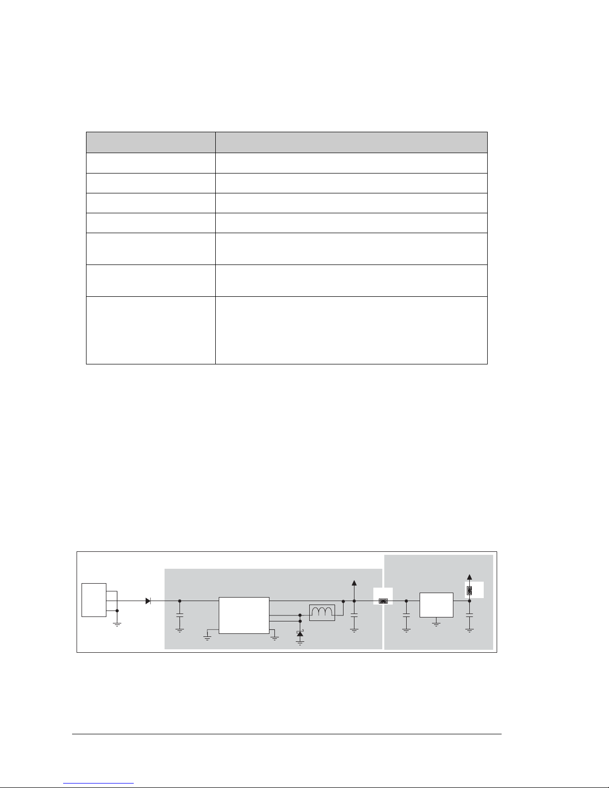
86 RabbitCore RCM4100
Table B-1 lists the electrical, mechanical, and environmental specifications for the Prototyping Board.
B.3 Power Supply
The RCM4100 series of modules requires a regulated 3.0 V – 3.6 V DC power source to
operate. Depending on the amount of current required by the application, different regulators can be used to supply this voltage.
The Prototyping Board has an onboard +5 V switching power regulator from which a
+3.3 V linear regulator draws its supply. Thus both +5 V and +3.3 V are available on the
Prototyping Board.
The Prototyping Board itself is protected against reverse polarity by a Shottky diode at D2
as shown in Figure B-3.
Figure B-3. Prototyping Board Power Supply
Table B-1. Prototyping Board Specifications
Parameter Specification
Board Size 3.80" × 3.80" × 0.48" (97 mm × 97 mm × 12 mm)
Operating T emperatu re 0°C to +70°C
Humidity 5% to 95%, noncondensing
Input Voltage 8 V to 24 V DC
Maximum Current Draw
(includi ng user-added circuits)
800 mA max. for +3.3 V supply,
1 A total +3.3 V and +5 V combined
Prototyping Area
1.3" × 2.0" (33 mm × 50 mm) throughhole, 0.1" spacing,
additional space for SMT components
Connectors
One 2 × 25 header socket, 1.27 mm pitch, to accept RCM4100
One 1 × 3 IDC header for power-supply connection
One 2 × 5 IDC RS-232 header, 0.1" pitch
Two unstuffed header locations for analog and RCM4100 signals
25 unstuffed 2-pin header locations for optional configurations
LINEAR POWER
REGULATOR
POWER
IN
J1
10 µF
LM 1117
U1
+3.3 V
3
1
2
1
2
3
DL4003
D2
47 µF
330 µF
+5 V
L1
C5
330 µH
D1
B140
SWITCHING POWER REGULATOR
DCIN
U2
LM2575
C6
C2
10 µF
C4
JP1
JP2
Page 91
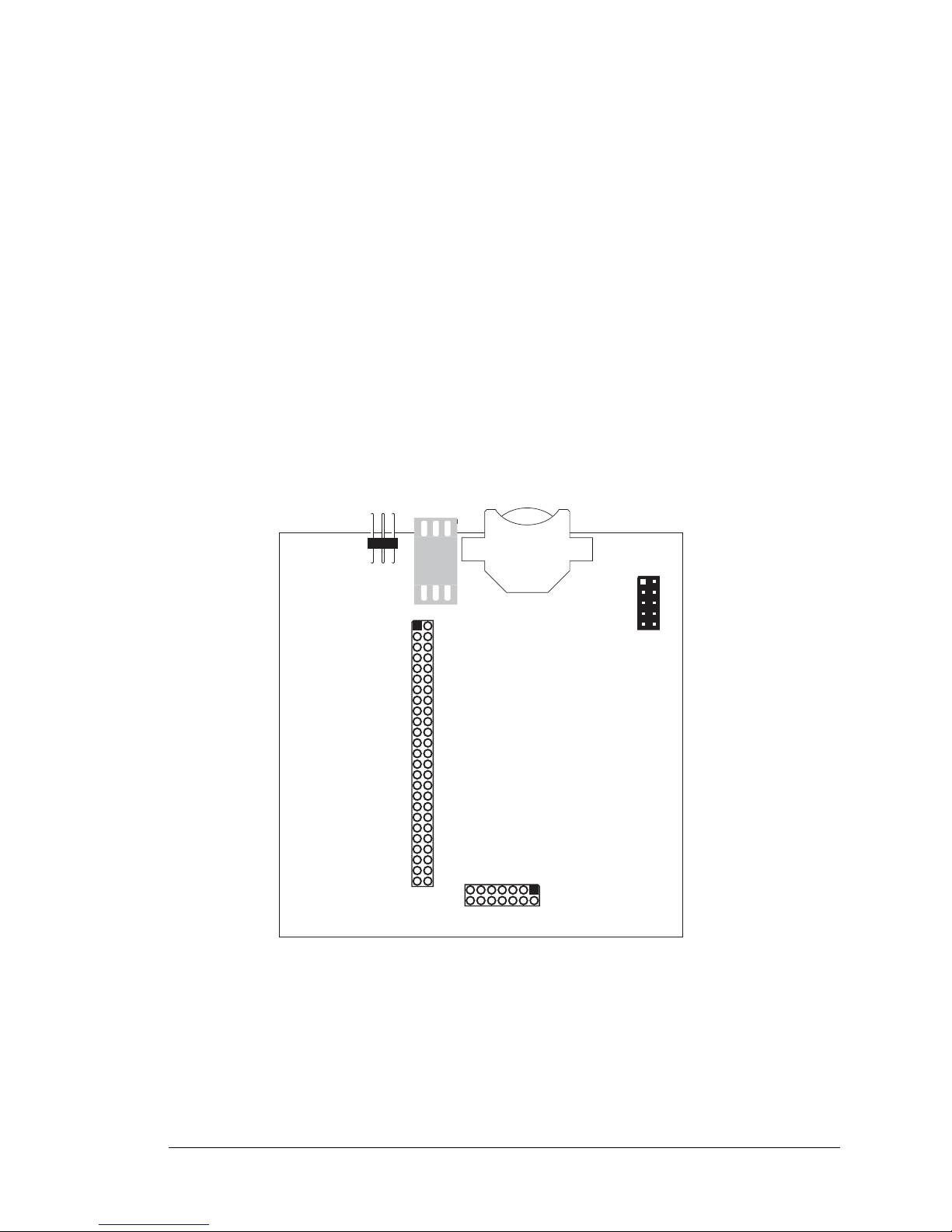
User’s Manual 87
B.4 Using the Prototyping Board
The Prototyping Board is actually both a demonstration board and a prototyping board. As
a demonstration board, it can be used to demonstrate the functionality of the
RCM4100
series of modules
right out of the box without any modifications to either board.
The Prototyping Board comes with the basic components necessary to demonstrate the
operation of the RCM4100. Two LEDs (DS2 and DS3) are connected to PB2 and PB3,
and two switches (S2 and S3) are connected to PB4 and PB5 to demonstrate the interface
to the Rabbit 4000 microprocessor . Reset switch S1 is the hardware reset for the RCM4100.
The
Prototyping Board provides the user with RCM4100 connection points brought out conveniently to labeled points at header J2 on the Prototyping Board. Although header J2 is
unstuffed, a 2 × 25 header is included in the bag of parts. RS-232 signals (Serial Ports C
and D)
are available on header J4. A header strip at J4 allows you to connect a ribbon cable,
and a ribbon cable to DB9 connector is included with the Development Kit.
The pinouts for
these locations are shown in Figure B-4.
Figure B-4. Prototyping Board Pinout
The analog signals are brought out to labeled points at header location J3 on the Prototyping
Board. Although header J3 is unstuffed, a 2 × 7 header can be added. Note that analog
signals are only available from the RCM4100 — the RCM4110 and RCM4120 models do
not have an A/D converter.
J4
J2
J3
+3.3 V
/RST_OUT
/IOWR
VBAT_EXT
PA1
PA3
PA5
PA7
PB1
PB3
PB5
PB7
PC1
PC3
PC5
PC7
PE1
PE3
PE5
PE7
PD1/LN1
PD3/LN3
PD5/LN5
PD7/LN7
VREF
GND
/IORD
/RST_IN
PA0
PA2
PA4
PA6
PB0
PB2
PB4
PB6
PC0
PC2
PC4
PC6
PE0
PE2
PE4
PE6
PD0/LN0
PD2/LN2
PD4/LN4
PD6/LN6
CVT
AGND
AGND
CVT
LN6IN
LN4IN
LN2IN
LN0IN
VREF
LN7IN
LN5IN
LN3IN
LN1IN
AGND
RCM4100
Signals
RS-232
Analog
Inputs
TxD
RxD
GND
RxC
TxC
J1
GND+GND
Page 92

88 RabbitCore RCM4100
Selected signals from the Rabbit 4000 microprocessor are available on header J2 of the
Prototyping Board. The remaining ports on the Rabbit 4000 microprocessor are used for
RS-232 serial communication. Table B-2 lists the signals on header J2 and explains how
they are used on the Prototyping Board.
There is a 1.3" × 2" through-hole prototyping space available on the Prototyping Board.
The holes in the prototyping area are spaced at 0.1" (2.5 mm).
+3.3 V, +5 V, and GND traces
run along the top edge of the prototyping area for easy access.
Small to medium circuits
can be prototyped using point-
to-point wiring with 20 to 30 AWG wire between the proto-
typing area, the
+3.3 V, +5 V, and GND traces,
and the surrounding area where surface-
mount components may be installed.
Small holes are provided around the surface-mounted
components that may be installed around the prototyping area.
Table B-2. Use of Rabbit 4000 Signals on the Prototypi ng Board
Pin Pin Name Prototyping Board Use
1 +3.3 V +3.3 V power supply
2 GND
3 /RST_OUT Reset output from reset generator
4 /IORD External read strobe
5 /IOWR External write strobe
6 /RESET_IN Input to reset generator
8–15 PA0–PA7 Output, pulled high
16 PB0 CLKB
17 PB1 Programming port CLKA
18 PB2 LED DS2 (normally high/off)
19 PB3 LED DS3 (normally high/off)
20 PB4 Switch S2 (normally open/pulled up)
21 PB5 Switch S3 (normally open/pulled up)
22–23 PB6–PB7 Output, pulled high
24–25 PC0–PC1 Serial Port D (RS-232, header J4) (high)
26–27 PC2–PC3 Serial Port C (RS-232, header J4) (high)
28–29 PC4–PC5 Serial Port B
30–31 PC6–PC7 Serial Port A (programming port) (high)
32–39 PE0–PE7 Parallel I/O, Output, I0–I7
40–47
LN0–LN7 A/D converter inputs (not available on RCM4110)
PD0–PD7 Output, pulled high
48 CONVERT A/D converter CONVERT input (not available on RCM4110)
49 VREF A/D converter reference voltage (not available on RCM4110)
50 AGND A/D converter ground (not available on RCM4110)
Page 93
User’s Manual 89
B.4.1 Adding Other Components
There are pads for 28-pin TSSOP devices, 16-pin SOIC devices, and 6-pin SOT devices
that can be used for surface-mount prototyping with these devices. There are also pads that
can be used for SMT resistors and capacitors in an 0805 SMT package. Each component
has every one of its pin pads connected to a hole in which a 30 A W G wire can be soldered
(standard wire wrap wire can be soldered in for point-to-point wiring on the Prototyping
Board). Because the traces are very thin, carefully determine which set of holes is connected to which surface-mount pad.
B.4.2 Measuring Current Draw
The Prototyping Board has a current-measurement feature available at header locations
JP1 and JP2 for the +5 V and +3.3 V supplies respectively. To measure current, you will
have to cut the trace on the bottom side of the Prototyping Board corresponding to the
power supply or power supplies whose current draw you will be measuring. Header locations JP1 and JP2 are shown in Figure B-5. Then install a 1 × 2 header strip from the
Development Kit on the top side of the Prototyping Board at the header location(s) whose
trace(s) you cut. The header strip(s) will allow you to use an ammeter across their pins to
measure the current drawn from that supply. Once you are done measuring the current,
place a jumper across the header pins to resume normal operation.
Figure B-5. Prototyping Board Current-Measur ement Option
NOTE: Once you have cut the trace below header location J P1 or JP2, you must e ither be
using the ammeter or have a jumper in place in order for power to be delivered to the
Prototyping Board.
A
0
Cut traces
Bottom Side
JP1
JP2
JP1 (+5 V)
or
JP2 (+3.3 V)
CURRENT
MEASUREMENT
D1
R1
PWR
DS1
GND
J1
U1
C1
GND
C2
JP1
C3
D2
JP2
L1
C6
C5
JP1
JP2
Page 94
90 RabbitCore RCM4100
B.4.3 Analog Features (RCM4100 only)
The Prototyping Board has typical support circuitry installed to complement the ADS7870
A/D converter on the RCM4100 model (the A/D converter is not available on the
RCM4110 and the RCM4120).
B.4.3.1 A/D Converter Inputs
Figure B-6 shows a pair of A/D converter input circuits. The resistors form an approx . 11 :1
attenuator, and the capacitor filters noise pulses from the A/D converter input. The 470 Ω
inline jumpers allow other configurations (see Table B-6) and provide digital isolation when
you are not using an A/D converter (Parallel Port D is available). These jumpers optimize
using RabbitCore modules w ith or without A/D co nverters—if you are designi ng your own
circuit, the best performance for the A/D converter would be realized with 0 Ω resistors.
Figure B-6. A/D Converter Inputs
The A/D converter chip can make either single-ended or differential measurements
depending on the value of the opmode parameter in the software function call. Adjacent
A/D converter inputs are paired to make differential measurements. The default setup on
the Prototyping Board is to measure only positive voltages for the ranges listed in Table B-3.
Table B-3. Positive A/D Converter Input Voltage Ranges
Min. Voltage
(V)
Max. Voltage
(with prescaler)
(V)
Gain
Multiplier
A/D Converter
Actual Gain
Resolution
(mV)
0.0 +22.528 ×1 1 11
0.0 +11.264 ×2 1.8 5.5
0.0 +5.632 ×4 3.6 2.75
0.0 +4.506 ×5 4.5 2.20
0.0 +2.816 ×8 7.2 1.375
0.0 +2.253 ×10 9.0 1.100
0.0 +1.408 ×16 14.4 0.688
0.0 +1.126 ×20 18 0.550
100 kW
LN0_IN
AGND
LN1_IN
ADC
BVREF =
2.048 V
100 kW
2.2 nF
10 kW
10 kW
2.2 nF
ADC
(RCM4100)
JP23/JP24
1
3
Inline jumpers are
470 W resistors
Page 95
User’s Manual 91
Many other possible ranges are possible by physically changing the resistor values that
make up the attenuator circuit.
NOTE: Analog input LN7_IN does not have the 10 kΩ resistor installed, and so no
resistor attenuator is ava il abl e, li mit in g its maximum inpu t vol ta ge to 2 V. This input is
intended to be used for a thermistor that you may install at header location JP25.
It is also possible to read a negative voltage on LN0_IN–LN5_IN by moving the 0 Ω
jumper (see Figure B-6) on header JP23 or JP24 associated with the A/D converter input
from analog ground to the reference voltage generated and buffered by the A/D converter.
Adjacent input channels are paired; moving the jumper on JP 23 changes both of the
paired channels (LN4_IN–LN5_IN), and moving the jumper on JP24 changes LN0_IN–
LN1_IN and LN2_IN–LN3_IN. At the present time Rabbit does not offer the software
drivers to work with single-ended negative voltages, but the differential mode described
below may be used to measure negative voltages.
Differential measurements require two channels. As the name differential implies, the dif-
ference in voltage between the two adjacent channels is measured rather than the difference between the input and analog ground. Voltage measurements taken in differential
mode have a resolution of 12 bits, with the 12th bit indicating whether the difference is
positive or negative.
The A/D converter chip can only a ccept positiv e voltages, as ex plained in Section 4.4. Both
different i al in pu t s mu st b e r e ferenced to analog ground, and both inpu t s mu s t be po siti ve
with respect to analog ground. Table B-4 provides the differential voltage ranges for this
setup.
Table B-4. Differential Voltage Ranges
Min. Differential
Voltage
(V)
Max. Differential
Voltage (with
prescaler)
(V)
Gain
Multiplier
A/D Converter
Actual Gain
Resolution
(mV)
0 ±22.528 ×1 1 11
0±11.264×21.8 5.5
0 ±5.632 ×4 3.6 2.75
0 ±4.506 ×5 4.5 2.20
0 ±2.816 ×8 7.2 1.375
0 ±2.253 ×10 9.0 1.100
0 ±1.408 ×16 14.4 0.688
0 ±1.126 ×20 18 0.550
Page 96

92 RabbitCore RCM4100
B.4.3.2 Thermistor Input
Analog input LN7_IN on the Prototyping Board was designed specifically for use with a
thermistor at JP25 in conjunction with the
THERMISTOR.C sample program, which demon-
strates how to use the analog input to measure temperature, which will be displayed in the
Dynamic C
STDIO window . The sample program is targeted specifically for the thermistor
included with the Development Kit with R
0
@ 25°C = 3 kΩ and β 25/85 = 3965. Be sure
to use the applicable R
0
and β values for your thermistor if you use another thermistor.
Figure B-7. Prototyping Board Thermistor Input
B.4.3.3 A/D Converter Calibration
T o get the best results form the A/D converter, it is necessary to calibrate each mode (singleended or differential) for each of its gains. It is imperative that you calibrate each of the
A/D converter inputs in the same manner as they are to be used in the application. For
example, if you will be performing floating differential measurements or differential measurements using a common analog ground, then calibrate the A/D converter in the corresponding manner. The calibration must be done with the JP23/JP24 selection jumpers in
the desired position (see Figure B-6). If a calibration is performed and a jumper is subsequently moved, the corresponding input(s) must be recalibrated. The calibration table in
software only holds calibration constants based on mode, channel, and gain. Ot her factors
affecting the calibration must be taken into account by calibrating using the same mode
and gain setup as in the intended use.
Sample programs are available to illustrate how to read and calibrate the various A/D
inputs for the single-ended operating mode.
Mode Read Calibrate
Single-Ended, one channel — AD_CAL_CHAN.C
Single-Ended, all channels AD_RDVOLT_ALL.C AD_CAL_ALL.C
9
1 kW
LN7_IN
BVREF
Thermistor
JP25
J3
2.2 nF
AGND
ADC
(RCM4100)
Inline jumper is
470 W resistor
Page 97

User’s Manual 93
B.4.4 Serial Communication
The Prototyping Board allows you to access five of the serial ports from the RCM4100
series of modules. T a ble B-5 summarizes the configuration options. Note that Serial Ports
E and F can be used only with the Prototyping Board.
Serial Ports E and F may be used as serial ports, or the corresponding pins at header location J2 may be used as parallel ports.
Table B-5. Prototyping Board Serial Port Configurations
Serial Port Header Default Use Alternate Use
A J2 Programming Port RS-232
BJ2
A/D Converter
(RCM4100 only)
—
C J2, J4 RS-232 —
D J2, J4 RS-232 —
EJ2 — —
FJ2 — —
Page 98

94 RabbitCore RCM4100
B.4.4.1 RS-232
RS-232 serial communication on header J4 on both Prototyping Boards is supported by an
RS-232 transceiver installed at U3. This transceiver provides the voltage output, slew rate,
and input voltage immunity required to meet the RS-232 serial communication protocol.
Basically, the chip translates the Rabbit 4000’s signals to RS-232 signal levels. Note that
the polarity is reversed in an RS-232 circuit so that a +3.3 V output becomes approximately -10 V and 0 V is output as +10 V. The RS-232 transceiver also provides the proper
line loading for reliable communication.
RS-232 can be us ed effectively at th e ma xim u m ba ud rat e for di s tan ce s of up to 15 m.
RS-232 flow control on an RS-232 port is initiated in software using the serXflowcon-
trolOn
function call from RS232.LIB, where X is the serial port (C or D). The locations
of the flow control lines are specified using a set of five macros.
SERX_RTS_PORT—Data register for the parallel port that the RTS line is on (e.g., PCDR).
SERA_RTS_SHADOW—Shadow register for the RTS line's parallel port (e.g., PCDRShadow).
SERA_RTS_BIT—The bit number for the RTS line.
SERA_CTS_PORT—Data register for the parallel port that the CTS line is on (e.g., PCDRShadow).
SERA_CTS_BIT—The bit number for the CTS line.
Standard 3-wire RS-232 communication using Serial Ports C and D is illustrated in the
following sample code.
#define CINBUFSIZE 15 // set size of circular buffers in bytes
#define COUTBUFSIZE 15
#define DINBUFSIZE 15
#define DOUTBUFSIZE 15
#define MYBAUD 115200 // set baud rate
#endif
main(){
serCopen(_MYBAUD); // open Serial Ports C and D
serDopen(_MYBAUD);
serCwrFlush(); // flush their input and transmit buffers
serCrdFlush();
serDwrFlush();
serDrdFlush();
serCclose(_MYBAUD); // close Serial Ports C and D
serDclose(_MYBAUD);
}
Page 99

User’s Manual 95
B.5 Prototyping Board Jumper Configurations
Figure B-8 shows the header locations used to configure the various Prototyping Board
options via jumpers.
Figure B-8. Location of Configurable Jumpers on Prototyping Board
T able B-6 lists the configuration options using either jumpers or 0 Ω surface-mount resistors.
Table B-6. Prototyping Board Jumper Confi gurations
Header Description Pins Connected
Factory
Default
JP1 +5 V Current Measurement 1–2 Via trace or jumper Connected
JP2 +3.3 V Current Measurement 1–2 Via trace or jumper Connected
JP3
JP4
PC0/TxD/LED DS2
JP3
1–2
TxD on header J4
×
JP4
1–2
PC0 to LED DS2
n.c. PC0 available on header J2
JP1
JP2
JP25
UX49
JP23
JP11
JP15
JP19
JP21
JP22
JP20
JP17
JP13
JP16
JP6
JP5
JP12
JP4
JP3
JP14
JP8
JP7
JP18
JP9
JP10
JP24
Page 100

96 RabbitCore RCM4100
JP5
JP6
PC1/RxD/Switch S2
JP5
1–2
RxD on header J4
×
JP6
1–2
PC1 to Switch S2
n.c. PC1 available on header J2
JP7
JP8
PC2/TxC/LED DS3
JP7
1–2
TxC on header J4
×
JP6
1–2
PC2 to LED DS3
n.c. PC2 available on header J2
JP9
JP10
PC3/RxC/Switch S3
JP9
1–2
PC3 to Switch S3
JP10
1–2
RxC on header J4
×
n.c. PC3 available on header J2
JP11 LN0 buffer/filter to RCM4100 1–2 Connected
JP12 PB2/LED DS2
1–2 Connected: PB2 to LED DS2
×
n.c. PB2 available on header J2
JP13 LN1 buffer/filter to RCM4100 1–2 Connected
JP14 PB3/LED DS3
1–2 Connected: PB3 to LED DS3
×
n.c. PB3 available on header J2
JP15 LN2 buffer/filter to RCM4100 1–2 Connected
JP16 PB4/Switch S2
1–2 Connected: PB4 to Switch S2
×
n.c. PB4 available on header J2
JP17 LN3 buffer/filter to RCM4100 1–2 Connected
JP18 PB5/Switch S3
1–2 Connected: PB5 to Switch S3
×
n.c. PB5 available on header J2
JP19 LN4 buffer/filter to RCM4100 1–2 Connected
JP20 LN5 buffer/filter to RCM4100 1–2 Connected
JP21 LN6 buffer/filter to RCM4100 1–2 Connected
JP22 LN7 buffer/filter to RCM4100 1–2 Connected
Table B-6. Prototyping Board Jumpe r Confi gurations (continued)
Header Description Pins Connected
Factory
Default
 Loading...