

Page 1

BL4S200
C-Programmable Single-Board Computer with Networking
User’s Manual
019–0171_E
Page 2

BL4S200 User’s Manual
Part Number 019-0171_D • Printed in U.S.A.
©2008–2010 Digi International Inc. • All rights reserved.
Digi International reserves the right to make changes and
improvements to its products without providing notice.
Trademarks
Rabbit, RabbitCore, and Dynamic C are registered trademarks of Digi International Inc.
RabbitNet is a trademark of Digi International Inc.
The latest revision of this manual is available on the Rabbit Web site, www.rabbit.com,
for free, unregistered download.
Digi International Inc.
www.rabbit.com
Page 3

TABLE OF CONTENTS
Chapter 1. Introduction 6
1.1 BL4S200 Description ...........................................................................................................................6
1.2 BL4S200 Features.................................................................................................................................6
1.3 Development and Evaluation Tools......................................................................................................8
1.3.1 Tool Kit .........................................................................................................................................8
1.3.2 Software ........................................................................................................................................9
1.3.3 Optional Add-Ons .........................................................................................................................9
1.4 RabbitNet Peripheral Cards ................................................................................................................10
1.5 CE Compliance ...................................................................................................................................11
1.5.1 Design Guidelines .......................................................................................................................12
1.5.2 Interfacing the BL4S200 to Other Devices.................................................................................12
1.6 Wi-Fi Certifications (BL5S220 Model only)......................................................................................13
1.6.1 FCC Part 15 Class B ...................................................................................................................13
1.6.2 Industry Canada Labeling ...........................................................................................................14
1.6.3 Europe .........................................................................................................................................15
Chapter 2. Getting Started 16
2.1 Preparing the BL4S200 for Development ..........................................................................................16
2.2 BL4S200 Connections ........................................................................................................................17
2.2.1 Hardware Reset ...........................................................................................................................18
2.3 Installing Dynamic C ..........................................................................................................................19
2.4 Starting Dynamic C ............................................................................................................................20
2.5 Run a Sample Program .......................................................................................................................20
2.5.1 Troubleshooting ..........................................................................................................................20
2.6 Run a Wi-Fi Sample Program (BL5S220 only)..................................................................................21
2.7 Run a ZigBee Sample Program (BL4S230 only) ...............................................................................22
2.8 Where Do I Go From Here? ...............................................................................................................23
Chapter 3. Subsystems 24
3.1 BL4S200 Pinouts ................................................................................................................................25
3.1.1 Connectors ..................................................................................................................................26
3.2 Digital I/O ...........................................................................................................................................27
3.2.1 Configurable I/O .........................................................................................................................27
3.2.2 High-Current Digital Outputs .....................................................................................................34
3.3 Serial Communication ........................................................................................................................36
3.3.1 RS-232 ........................................................................................................................................36
3.3.2 RS-485 ........................................................................................................................................36
3.3.3 Programming Port .......................................................................................................................38
3.3.4 Ethernet Port ...............................................................................................................................39
3.4 A/D Converter Inputs..........................................................................................................................40
3.4.1 A/D Converter Calibration..........................................................................................................42
3.5 D/A Converter Outputs.......................................................................................................................43
3.5.1 D/A Converter Calibration..........................................................................................................44
3.6 Analog Reference Voltages Circuit ....................................................................................................45
3.7 USB Programming Cable ...................................................................................................................46
3.7.1 Changing Between Program Mode and Run Mode ....................................................................46
BL4S200 User’s Manual 3
Page 4

3.8 Other Hardware...................................................................................................................................47
3.8.1 Clock Doubler .............................................................................................................................47
3.8.2 Spectrum Spreader ......................................................................................................................48
3.9 Memory...............................................................................................................................................49
3.9.1 SRAM .........................................................................................................................................49
3.9.2 Flash Memory .............................................................................................................................49
3.9.3 VBAT RAM Memory.................................................................................................................49
3.9.4 microSD™ Cards ........................................................................................................................49
Chapter 4. Software 51
4.1 Running Dynamic C ...........................................................................................................................51
4.1.1 Upgrading Dynamic C ................................................................................................................53
4.1.2 Add-On Modules.........................................................................................................................53
4.2 Sample Programs ................................................................................................................................54
4.2.1 Digital I/O ...................................................................................................................................55
4.2.2 Serial Communication.................................................................................................................60
4.2.3 A/D Converter Inputs..................................................................................................................62
4.2.4 D/A Converter Outputs ...............................................................................................................64
4.2.5 Use of microSD™ Cards with BL4S200 Model.........................................................................66
4.2.6 Real-Time Clock .........................................................................................................................66
4.2.7 TCP/IP Sample Programs ...........................................................................................................66
4.3 BL4S200 Libraries..............................................................................................................................67
4.4 BL4S200 Function Calls.....................................................................................................................68
4.4.1 Board Initialization .....................................................................................................................68
4.4.2 Digital I/O ...................................................................................................................................69
4.4.3 High-Current Outputs .................................................................................................................92
4.4.4 Rabbit RIO Interrupt Handlers..................................................................................................104
4.4.5 Serial Communication...............................................................................................................108
4.4.6 A/D Converter Inputs................................................................................................................110
4.4.7 D/A Converter Outputs .............................................................................................................123
4.4.8 SRAM Use ................................................................................................................................131
Chapter 5. Using the Ethernet TCP/IP Features 132
5.1 TCP/IP Connections .........................................................................................................................132
5.2 TCP/IP Sample Programs .................................................................................................................134
5.2.1 How to Set IP Addresses in the Sample Programs ...................................................................134
5.2.2 How to Set Up your Computer for Direct Connect ..................................................................135
5.2.3 Run the
5.2.4 Running More Demo Programs With a Direct Connection......................................................137
5.3 Where Do I Go From Here? .............................................................................................................137
PINGME.C Demo ....................................................................................................136
Chapter 6. Using the Wi-Fi Features 138
6.1 Introduction to Wi-Fi ........................................................................................................................138
6.1.1 Infrastructure Mode...................................................................................................................138
6.1.2 Ad-Hoc Mode ...........................................................................................................................139
6.1.3 Additional Information .............................................................................................................139
6.2 Running Wi-Fi Sample Programs.....................................................................................................140
6.2.1 Wi-Fi Setup...............................................................................................................................141
6.2.2 What Else You Will Need.........................................................................................................142
6.2.3 Configuration Information ........................................................................................................143
6.2.4 Wi-Fi Sample Programs............................................................................................................146
6.2.5 RCM5400W Sample Programs.................................................................................................151
6.3 Dynamic C Wi-Fi Configurations.....................................................................................................154
6.3.1 Configuring TCP/IP at Compile Time ......................................................................................154
6.3.2 Configuring TCP/IP at Run Time .............................................................................................158
6.3.3 Other Key Function Calls .........................................................................................................158
6.4 Where Do I Go From Here? .............................................................................................................159
BL4S200 User’s Manual 4
Page 5

Chapter 7. Using the ZigBee Features 160
7.1 Introduction to the ZigBee Protocol .................................................................................................160
7.2 ZigBee Sample Programs .................................................................................................................161
7.2.1 Setting Up the Digi XBee USB Coordinator ............................................................................162
7.2.2 Setting up Sample Programs .....................................................................................................164
7.3 Dynamic C Function Calls................................................................................................................167
7.4 Where Do I Go From Here? .............................................................................................................167
Appendix A. Specifications 168
A.1 Electrical and Mechanical Specifications ........................................................................................169
A.1.1 Exclusion Zone.........................................................................................................................173
A.1.2 Headers.....................................................................................................................................173
A.2 Conformal Coating...........................................................................................................................174
A.3 Jumper Configurations.....................................................................................................................175
A.4 Use of Rabbit Microprocessor Parallel Ports ...................................................................................177
Appendix B. Power Supply 178
B.1 Power Supplies.................................................................................................................................178
B.1.1 Power for Analog Circuits........................................................................................................179
B.2 Batteries and External Battery Connections ....................................................................................179
B.2.1 Replacing the Backup Battery..................................................................................................180
B.3 Power to Peripheral Cards................................................................................................................181
Appendix C. Demonstration Board 182
C.1 Connecting Demonstration Board....................................................................................................183
C.2 Demonstration Board Features.........................................................................................................184
C.2.1 Pinout........................................................................................................................................184
C.2.2 Configuration............................................................................................................................184
Appendix D. Rabbit RIO Resource Allocation 186
D.1 Configurable I/O Pin Associations ..................................................................................................187
D.2 High-Current Output Pin Associations ............................................................................................188
D.3 Interpreting Error Codes ..................................................................................................................188
Appendix E. RabbitNet 190
E.1 General RabbitNet Description ........................................................................................................190
E.1.1 RabbitNet Connections.............................................................................................................190
E.1.2 RabbitNet Peripheral Cards ......................................................................................................191
E.2 Physical Implementation ..................................................................................................................192
E.2.1 Control and Routing .................................................................................................................192
E.3 Function Calls...................................................................................................................................193
E.3.1 Status Byte................................................................................................................................203
Appendix F. Additional Configuration Instructions 204
F.1 XBee Module Firmware Downloads................................................................................................204
F.1.1 Dynamic C v. 10.44 and Later..................................................................................................204
F.2 Digi
®
XBee USB Configuration ......................................................................................................205
F.2.1 Additional Reference Information ............................................................................................206
F.2.2 Update Digi
®
XBee USB Firmware.........................................................................................208
Index 209
Schematics 213
BL4S200 User’s Manual 5
Page 6

1. INTRODUCTION
The BL4S200 series of high-performance, C-programmable singleboard computers offers built-in digital and analog I/O combined
with Ethernet, Wi-Fi, or ZigBee network connectivity in a compact form factor. The BL4S200 single-board computers are ideal
for both discrete manufacturing and process-control applications.
®
A Rabbit
data processing. A removable flash memory option supports a
full directory file structures to maximize remote access control
and programmability. The I/O can be expanded with RabbitNet
peripheral cards.
1.1 BL4S200 Description
Throughout this manual, the term BL4S200 refers to the complete series of BL4S200 singleboard computers unless other production models are referred to specifically.
4000 or Rabbit® 5000 microprocessor provides fast
The BL4S200 is an advanced single-board computer that incorporates the powerful Rabbit
4000 or Rabbit 5000 microprocessor, flash memory options, static RAM, digital I/O ports,
A/D converter inputs, D/A converter outputs, RS-232/RS-485 serial ports, and Ethernet,
Wi-Fi, or ZigBee network connectivity.
1.2 BL4S200 Features
• Rabbit® 4000 or Rabbit® 5000 microprocessor operating at up to 73.73 MHz.
• Industry-standard Micro-Fit® polarized positive-locking connectors.
• 512KB SRAM and 512KB/1MB flash memory options.
• 40 digital I/O: 32 protected digital I/O individually software-configurable as inputs or
sinking outputs, and 8 high-current digital outputs software-configurable as sinking or
sourcing.
• Advanced input capabilities including event counting, event capture, and quadrature
decoders that may be set up on most I/O pins.
• Independent PWM and PPM capability on most I/O pins and all high-current outputs.
• 10 analog channels: eight 11-bit A/D converter inputs, two 12-bit D/A converter 0–10 V
or ±10 V buffered outputs.
BL4S200 User’s Manual 6
Page 7

• Ethernet, Wi-Fi, or ZigBee network connectivity.
• Up to 5 serial ports:
Up to three serial ports (one 5-wire RS-232 or two 3-wire RS-232, one RS-485).
Two RabbitNet™ expansion ports multiplexed from one serial port.
One serial port dedicated to programming/debugging.
• Battery-backed real-time clock.
• Watchdog supervisor.
Four BL4S200 models are available. Their standard features are summarized in Table 1.
Table 1. BL4S200 Models
Feature
Microprocessor
Program Execution
SRAM
Data SRAM 512KB 512KB 512KB 512KB
Flash Memory (program)
Flash Memory
(data storage)
Network Interface
RabbitCore Module Used RCM4310 RCM4010 RCM5400W RCM4510W (ZB)
BL4S200 BL4S210 BL5S220 BL4S230
®
Rabbit
512KB — 512KB —
1MB
(serial flash)
supports
microSD™
Card
128MB–1GB
10/100Base-T,
3 LEDs
4000 running
at 58.98 MHz
512KB
(parallel flash)
—
10Base-T,
2 LEDs
Rabbit® 5000 running
at 73.73 MHz
512KB
(parallel flash)
1MB
(serial flash)
Wi-Fi (802.11b/g)
Rabbit® 4000 running
at 29.49 MHz
512KB
(parallel flash)
ZigBee 2007
(802.15.4)
Note that the BL5S220 model is named as such to reflect that it uses a Rabbit 5000 microprocessor.
BL4S200 single-board computers consist of a main board with a RabbitCore module.
Refer to the RabbitCore module manuals, available on the Web s ite , for more information
on the RabbitCore modules, including their schematics.
BL4S200 single-board computers are programmed over a standard PC USB port through a
programming cable supplied with the Tool Kit. The BL4S200 and BL5S220 models may
also be programmed remotely using the Remote Program Update library with Dynamic C
v. 10.54 or later. See Application Note AN421, Remote Program Update, for more
information.
NOTE: BL4S200 Series single-board computers cannot be programmed via the RabbitLink.
Appendix A provides detailed specifications.
Visit the We b sit e for up-to-date information about additional add-ons and features as
they become available. The Web site also has the latest revision of this user’s manual.
BL4S200 User’s Manual 7
Page 8
1.3 Development and Evaluation Tools
Rabbit, Dynamic C, and Digi are registered trademarks of Digi International Inc.
SD is a trademark of the SD Card Association.
BL4S200
The BL4S200 is a fully loaded series of single-board computers that feature built-in Ethernet, Wi-Fi, or
ZigBee network connectivity, configurable I/O, high-current outputs, RS-232 and RS-485 serial I/O, and
an A/D converter. These Getting Started instructions included with the Tool Kit will help you get your
BL4S200 up and running so that you can run the sample programs to explore its capabilities and develop
your own applications.
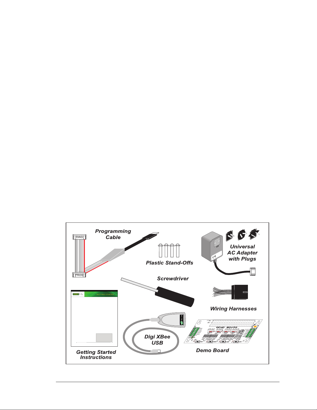
Tool Kit Contents
t
Getting Started instructions.
t
Dynamic C CD-ROM, with complete product documentation on disk.
t
USB programming cable, used to connect your PC USB port to the BL4S200.
t
Universal AC adapter, 12 V DC, 1 A (includes Canada/Japan/U.S., Australia/N.Z., U.K., and
European style plugs).
t
Digi® XBee USB (used as ZigBee coordinator for BL4S230 model).
t
Stand-offs to serve as legs for the BL4S200 board during development.
t
Demonstration Board with pushbutton switches and LEDs. The Demonstration Board can be
hooked up to the BL4S200 to demonstrate the I/O
and capabilities of the BL4S200.
t
Cable assemblies with Micro-Fit® connectors.
t
Screwdriver.
t
Rabbit 4000 Processor Easy Reference and Rabbit
5000 Processor Easy Reference posters.
t
Registration card.
Installing Dynamic C
®
Insert the CD from the Development Kit in
your PC’s CD-ROM drive. If the installation
does not auto-start, run the set up.exe pro-
gram in the root directory of the Dynamic C
CD. Install any Dynamic C modules after you
install Dynamic C
.
1.3.1 Tool Kit
A Tool Kit contains the hardware essentials you will need to use your own BL4S200 singleboard computer. These items are supplied in the Tool Kit.
• Getting Started instructions.
• Dynamic C CD-ROM, with complete product documentation on disk.
• USB programming cable, used to connect your PC USB port to the BL4S200.
• Universal AC adapter, 12 V DC, 1 A (includes Canada/Japan/U.S., Australia/N.Z.,
U.K., and European style plugs).
• Stand-offs to serve as legs for the BL4S200 board during development.
• Demonstration Board with pushbutton switches and LEDs. The Demonstration Board
can be hooked up to the BL4S200 to demonstrate the I/O and capabilities of the
BL4S200.
• CAT 5/6 Ethernet crossover cable.
• Cable assemblies with Micro-Fit® connectors.
• Rabbit 4000 Processor Easy Reference and Rabbit 5000 Processor Easy Reference
posters.
• Screwdriver.
• Registration card.
Figure 1. BL4S200 Tool Kit
BL4S200 User’s Manual 8
Page 9

1.3.2 Software
The BL4S200 is programmed using version 10.42 or later of Rabbit’s Dynamic C. A com-
patible version is included on the Tool Kit CD-ROM.
This version of Dynamic C includes the
popular µC/OS-II real-time operating system, point-to-point protocol (PPP), FAT file
system, RabbitWeb, and the Rabbit Embedded Security Pack featuring the Secure Sockets
Layer (SSL) and a specific Advanced Encryption Standard (AES) library.
In addition to the Web-based technical support included at no extra charge, a one-year
telephone-based technical support subscription is also available for purchase. Visit our
Web site at www.rabbit.com for further information and complete documentation, or contact your Rabbit sales representative or authorized distributor
1.3.3 Optional Add-Ons
Rabbit has available a Mesh Network Add-On Kit and additional tools and parts to help
you to make your own wiring assemblies with the friction-lock connectors.
• Mesh Network Add-On Kit (Part No. 101-1272)
Digi
XBee Series 2 RF module
RF Interface module
®
XBee USB (used as ZigBee coordinator)
The XBee Series 2 RF module is installed on the RF Interface module, which can be
connected via an RS-232 serial connection to a Windows PC for setup. The Mesh
Network Add-On Kit enables you to explore the wireless capabilities of the BL4S230
model that offers a ZigBee network interface.
• Connector Cable Assemblies (Part No. 151-0153)—Two 2 × 5 friction-lock connectors
(3 mm pitch) assembled with wiring harness.
• Crimp tool (Part No. 998-0013) to secure wire in crimp terminals.
Visit our Web site at www.rabbit.com or contact your Rabbit sales representative or authorized distributor for further information.
BL4S200 User’s Manual 9
Page 10

1.4 RabbitNet Peripheral Cards
RabbitNet™ is an SPI serial protocol that uses a robust RS-422 differential signalling
interface (twisted-pair differential signaling) to run at a fast 1 Megabit per second serial
rate. BL4S200 single-board computers have two RabbitNet ports, each of which can support one peripheral card. Distances between a master processor unit and peripheral cards
can be up to 10 m or 33 ft.
The following low-cost peripheral cards are currently available.
• Digital I/O
• A/D converter
• D/A converter
• Relay card
• Display/Keypad interface
Appendix E provides additional information on RabbitNet peripheral cards and the RabbitNet protocol. Visit our We b sit e for up-to-date information about additional add-ons and
features as they become available.
BL4S200 User’s Manual 10
Page 11

1.5 CE Compliance
Equipment is generally divided into two classes.
CLASS A CLASS B
Digital equipment meant for light industrial use Digital equipment meant for home use
Less restrictive emissions requirement:
less than 40 dB µV/m at 10 m
(40 dB relative to 1 µV/m) or 300 µV/m
More restrictive emissions requirement:
30 dB µV/m at 10 m or 100 µV/m
These limits apply over the range of 30–230 MHz. The limits are 7 dB higher for frequencies above 230 MHz. Although the test range goes to 1 GHz, the emissions from Rabbitbased systems at frequencies above 300 MHz are generally well below background noise
levels.
The BL4S200 single-board computer has been tested and was found to
be in conformity with the following applicable immunity and emission
standards. The BL4S210, BL5S220, and BL4S230 single-board
computers are also CE qualified as they are sub-versions of the BL4S200
single-board computer. Boards that are CE-compliant have the CE mark.
Immunity
The BL4S200 series of single-board computers meets the following EN55024/1998
immunity standards.
• EN61000-4-3 (Radiated Immunity)
• EN61000-4-4 (EFT)
• EN61000-4-6 (Conducted Immunity)
Additional shielding or filtering may be required for a heavy industrial environment.
Emissions
The BL4S200 series of single-board computers meets the following emission standards.
• EN55022:1998 Class B
• FCC Part 15 Class B
Your results may vary, depending on your application, so additional shielding or filtering
may be needed to maintain the Class B emission qualification.
BL4S200 User’s Manual 11
Page 12

1.5.1 Design Guidelines
Note the following requirements for incorporating the BL4S200 series of single-board
computers into your application to comply with CE requirements.
General
• The power supply provided with the Tool Kit is for development purposes only. It is the
customer’s responsibility to provide a CE-compliant power supply for the end-product
application.
• When connecting the BL4S200 single-board computer to outdoor cables, the customer
is responsible for providing CE-approved surge/lighting protection.
• Rabbit recommends placing digital I/O or analog cables that are 3 m or longer in a
metal conduit to assist in maintaining CE compliance and to conform to good cable
design practices.
• When installing or servicing the BL4S200, it is the responsibility of the end-user to use
proper ESD precautions to prevent ESD damage to the BL4S200.
Safety
• All inputs and outputs to and from the BL4S200 series of single-board computers must
not be connected to voltages exceeding SELV levels (42.4 V AC peak, or 60 V DC).
• The lithium backup battery circuit on the BL4S200 single-board computer has been
designed to protect the battery from hazardous conditions such as reverse charging and
excessive current flows. Do not disable the safety features of the design.
1.5.2 Interfacing the BL4S200 to Other Devices
Since the BL4S200 series of single-board computers is designed to be connected to other
devices, good EMC practices should be followed to ensure compliance. CE compliance is
ultimately the responsibility of the integrator. Additional information, tips, and technical
assistance are available from your authorized Rabbit distributor, and are also available on
our Web site at www.rabbit.com.
BL4S200 User’s Manual 12
Page 13

1.6 Wi-Fi Certifications (BL5S220 Model only)
The systems integrator and the end-user are ultimately responsible for the channel range
and power limits complying with the regulatory requirements of the country where the end
device will be used. Dynamic C function calls and sample programs illustrate how this is
achieved by selecting the country or region, which sets the channel range and power limits
automatically. See Section 6.2.4.1 for additional information and sample programs demonstrating how to configure an end device to meet the regulatory channel range and power
limit requirements.
Only RCM5400W modules bearing the FCC certification are certified for use in Wi-Fi
enabled end devices associated with the BL5S220 model, and any applications must have
been compiled using Dynamic C v. 10.40 or later. The certification is valid only for
RCM5400W modules equipped with the dipole antenna that is included with the modules,
or a detachable antenna with a 60 cm coaxial cable (Digi International part number
29000105). Changes or modifications to this equipment not expressly approved by Digi
International may void the user's authority to operate this equipment.
In the event that these conditions cannot be met, then the FCC certification is no longer
considered valid and the FCC ID can not be used on the final product. In these circumstances, the systems integrator or end-user will be responsible for re-evaluating the end
device (including the transmitter) and obtaining a separate FCC certification.
NOTE: Any regulatory certification is voided if the RF shield on the RCM5400W
module is removed.
1.6.1 FCC Part 15 Class B
The RCM5400W RabbitCore module has been tested and found to comply with the limits
for Class B digital devices pursuant to Part 15 Subpart B, of the FCC Rules. These limits
are designed to provide reasonable protection against harmful interference in a residential
environment. This equipment generates, uses, and can radiate radio frequency energy, and
if not installed and used in accordance with the instruction manual, may cause harmful
interference to radio communications. However, there is no guarantee that interference
will not occur in a particular installation. If this equipment does cause harmful interference to radio or television reception, which can be determined by turning the equipment
off and on, the user is encouraged to try and correct the interference by one or more of the
following measures:
• Reorient or relocate the receiving antenna.
• Increase the separation between the equipment and the receiver.
• Connect the equipment into an outlet on a circuit different from that to which the
receiver is connected.
• Consult the dealer or an experienced radio/TV technician for help.
BL4S200 User’s Manual 13
Page 14

Labeling Requirements (FCC 15.19)
FCC ID: VCB-E59C4472
This device complies with Part 15 of FCC rules. Operation is
subject to the following two conditions:
(1) this device may not cause harmful interference, and
(2) this device must accept any interference received, including
interference that may cause undesired operation.
If the FCC identification number is not visible when the module is installed inside another
device, then the outside of the device into which the module is installed must also display
a label referring to the enclosed module or the device must be capable of displaying the
FCC identification number electronically. This exterior label can use wording such as the
following: “Contains Transmitter Module FCC ID: VCB-E59C4472” or “Contains FCC
ID: VCB-E59C4472.” Any similar wording that expresses the same meaning may be used.
The following caption must be included with documentation for any device incorporating
the RCM5400W RabbitCore module.
Caution — Exposure to Radio-Frequency Radiation.
To comply with FCC RF exposure compliance requirements, for mobile
configurations, a separation distance of at least 20 cm must be maintained
between the antenna of this device and all persons.
This device must not be co-located or operating in conjunction with any
other antenna or transmitter.
1.6.2 Industry Canada Labeling
7143A-E59C4472
This Class B digital apparatus complies with Canadian standard
ICES-003.
Cet appareil numérique de la classe B est conforme à la norme
NMB-003 du Canada.
BL4S200 User’s Manual 14
Page 15

1.6.3 Europe
The marking shall include as a minimum:
• the name of the manufacturer or his trademark;
• the type designation;
• equipment classification, (see below).
Receiver
Class
1
2
3
Highly reliable SRD communication media, e.g., serving human life
inherent systems (may result in a physical risk to a person).
Medium reliable SRD communication media, e.g., causing
inconvenience to persons that cannot be overcome by other means.
Standard reliable SRD communication media,e.g., inconvenience to
persons that can simply be overcome by other means.
Risk Assessment of Receiver Performance
NOTE: Manufacturers are recommended to declare the classification of their devices in
accordance with Table 2 and EN 300 440-2 [5] clause 4.2, as relevant. In particular,
where an SRD that may have inherent safety of human life implications, manufacturers
and users should pay particular attention to the potential for interference from other
systems operating in the same or adjacent bands.
Regulatory Marking
The equipment shall be marked, where applicable, in accordance with CEPT/ERC Recommendation 70-03 or Directive 1999/5/EC, whichever is applicable. Where this is not
applicable, the equipment shall be marked in accordance with the National Regulatory
requirements.
BL4S200 User’s Manual 15
Page 16

2. GETTING STARTED
RESET
S1
S2
R
1
CORE +3.3 V
DS1
DS2
J9
J10
J11
J12
J8
J7
J6
J5
J4
J3
J2
J1
RCM1
R7
R8
R9
R10
C63
JP4
JP5
JP6
JP3
C62
C47
JP7
RS485
JP9
JP8
KB
+5 V
GND+3.3 v
KA
+5 V
GND+3.3 V
C52
C55
C57
C61
C56
C60
C50
C51
C49
C59
C54
C48
C53
C58
U7
C38
C39
C
40
C21
C27
C33
C17
C19
C25
C
14
R4
R2
C12
C13 U5
U6
C16
C41
C42
C
43
C23
C29
C35
C22
C28
C34
U8
C44
C45
C46
C24
C30
C36
R117
RP1
U4
C37
RP2
R5
R121
L2 L3
BT1
C31
C32
U3
C15
C10
U2
C11
C9
C8
U1
R116
R3
R118
C18
C20
C26
JP1
JP2
D2
D3
L1
D4
C1
C2
C3
C4
C6
TERMTE
R
M
K
C
+5 V
GN
D
+3.3 V
KD
+5 V
G
ND
+3.3 V
CAUTION! HOT!
CAUTION! HOT!
D6 D5 D8 D7
D9
C5
C7
D10
DS4
DS3
R6
BOARD
+3.3 V
POWER
IN
RNET PWR
4
1
7
14
8
R13
R12
R11
6
10
5
6
10
5
6
10
5
2
4
3
6
10
5
D1
6
10
5
6
10
5
610
5
Battery
D56
D57
D58
D59
D60
RabbitCore
Module
J1
R1
R2
R19
R3
R4
C3
L1
C1
C2
Y1
4
1
3
R16
R17
C4
C8
C5
C6
C7
R20
U2
R21
R22
R23
C13
C12
L2
C10
JP15
C21
U7
R38
J2
R37
R36
C22
DS1
LINK
SPEED
FD
X
DS3
DS2
R39
R40
R41
R35
C23
R34
U6
R33
R31
R32
D1
R66
C14
C11
C9
R7
R6
DS4
R42
J3
U18
R65
R67
R64
R29
R68
R69
R30
R24
C15 C16 R28 R27 R26
R25
C20
U5
JP12
JP13
JP14
R71
R70
R5
JP1
JP2
R72
JP3
JP4
JP5
JP6
JP7
JP8
JP9
JP10
JP11
U3
R8
R9
Q2
Q3
C91
C93
U1
R10
R11
R13
R12
R14
R15
C17
C18
C19
C92
C90
Chapter 2 explains how to connect the programming cable and
power supply to the BL4S200.
2.1 Preparing the BL4S200 for Development
Position the BL4S200 as shown below in Figure 2. Attach the four stand-offs supplied
with the Tool Kit in the holes at the corners as shown.
Figure 2. Attach Stand-Offs to BL4S200 Board
The stand-offs facilitate handling the BL4S200 during development, and protect the bottom of the printed circuit board against scratches or short circuits while you are working
with the BL4S200.
NOTE: If you ever need to remove the RabbitCore module, take care to keep the BL4S200
main boards and their corresponding RabbitCore modules paired since the RabbitCore
modules store calibration constants specific to the BL4S200 main board to which they
are plugged in. If you use a RabbitCore module from a different model in the BL4S200
series, your specific BL4S200 model may no longer operate as designed.
BL4S200 User’s Manual 16
Page 17

2.2 BL4S200 Connections
RESET
S1
S2
R1
CORE +3.3 V
DS1
DS2
J9
J10
J11
J12
J8
J7
J6
J5
J4
J3
J2
J1
RCM1
R7
R8
R9
R10
C63
JP4
JP5
JP6
JP3
C62
C47
JP7
RS485
JP9
JP8
KB
+5 V
GND
+3.3 v
KA
+5 V
GND
+3.3 V
C52
C55
C57
C61
C56
C60
C50
C51
C49
C59
C54
C48
C53
C58
U7
C38
C39
C40
C21
C27
C33
C17
C19
C25
C14
R4
R2
C12
C13 U5
U6
C16
C41
C42
C43
C23
C29
C35
C22
C28
C34
U8
C44
C45
C46
C24
C30
C36
R117
RP1
U4
C37
RP2
R5
R121
L2 L3
BT1
C31
C32
U3
C15
C10
U2
C11
C9
C8
U1
R116
R3
R118
C18
C20
C26
JP1
JP2
D2
D3
L1
D4
C1
C2
C3
C4
C6
TERM
TERM
KC
+5 V
GND
+3.3 V
KD
+5 V
GND
+3.3 V
CAUTION! HOT!
CAUTION! HOT!
D6 D5 D8 D7
D9
C5
C7
D10
DS4
DS3
R6
BOARD
+3.3 V
POWER
IN
RNET PWR
4
1
7
14
8
R13
R12
R11
6
10
5
6
10
5
6
10
5
2
4
3
6
10
5
D1
6
10
5
6
10
5
610
5
Battery
D56
D57
D58
D59
D60
J1
R1
R2
R19
R3
R4
C3
L1
C1
C2
Y1
4
1
3
R16
R17
C4
C8
C5
C6
C7
R20
U2
R21
R22
R23
C13
C12
L2
C10
JP15
C21
U7
R38
J2
R37
R36
C22
DS1
LINK
SPEED
FDX
DS3
DS2
R39
R40
R41
R35
C23
R34
U6
R33
R31
R32
D1
R66
C14
C11
C9
R7
R6
DS4
R42
J3
U18
R65
R67
R64
R29
R68
R69
R30
R24
C15 C16 R28 R27 R26
R25
C20
U5
JP12
JP13
JP14
R71
R70
R5
JP1
JP2
R72
JP3
JP4
JP5
JP6
JP7
JP8
JP9
JP10
JP11
U3
R8
R9
Q2
Q3
C91
C93
U1
R10
R11
R13
R12
R14
R15
C17
C18
C19
C92
C90
Colored
edge
To
PC USB port
PROG
DIAG
Programming
Cable
PROG
J1
1. Connect the programming cable to download programs from your PC and to program
and debug the BL4S200.
Connect the 10-pin PROG connector of the programming cable to header J1 on the
BL4S200’s RabbitCore module (the programming header is labeled J2 on the BL5S220
and BL4S230 models). Ensure that the colored edge lines up with pin 1 as shown. (Do not
use the DIAG connector, which is used for monitoring only.) Connect the other end of the
programming cable to an available USB port on your PC or workstation.
Connect the other end of the programming cable to an available USB port on your PC or
workstation.
Your PC should recognize the new USB hardware, and the LEDs in the shrink-wrapped
area of the USB programming cable will flash — if you get an error message, you will
have to install USB drivers. Drivers for Windows XP are available in the Dynamic C
Drivers\Rabbit USB Programming Cable\WinXP_2K folder — double-click
DPInst.exe to install the USB drivers. Drivers for other operating systems are available
online at www.ftdichip.com/Drivers/VCP.htm.
BL4S200 User’s Manual 17
Figure 3. Programming Cable Connections
NOTE: Never disconnect the programming cable by pulling on the ribbon cable.
Carefully pull on the connector to remove it from the header.
Page 18

2. Connect the power supply to header J5 on the BL4S200 as shown in Figure 4. Be sure
to match the latch mechanism with the top of the connector to header J5 on the
BL4S200 as shown. The Micro-Fit® connector will only fit one way.
Figure 4. Power Supply Connections
3. Apply power.
Once all the other connections have been made, you may connect power to the BL4S200.
First, prepare the AC adapter for the country where it will be used by selecting the plug.
The Tool Kit presently includes Canada/Japan/U.S., Australia/N.Z., U.K., and European
style plugs. Snap in the top of the plug assembly into the slot at the top of the AC adapter
as shown in Figure 4, then press down on the spring-loaded clip below the plug assembly
to allow the plug assembly to click into place. Release the clip to secure the plug assembly
in the AC adapter.
Plug in the AC adapter. The red LED next to the power connector at J5 should light up.
The BL4S200 is now ready to be used.
CAUTION: Unplug the power supply while you make or otherwise work with the connections
to the headers. This will protect your BL4S200 from inadvertent shorts or power spikes.
2.2.1 Hardware Reset
A hardware reset is done by unplugging the power supply, then plugging it back in, or by
pressing the RESET button located just below the RabbitCore module.
BL4S200 User’s Manual 18
Page 19

2.3 Installing Dynamic C
If you have not yet installed Dynamic C version 10.42 (or a later version), do so now by
inserting the Dynamic C CD from the BL4S200 Tool Kit in your PC’s CD-ROM drive. If
autorun is enabled, the CD installation will begin automatically.
If autorun is disabled or the installation does not start, use the Windows Start | Run menu
or Windows Disk Explorer to launch setup.exe from the root folder of the CD-ROM.
The installation program will guide you through the installation process. Most steps of the
process are self-explanatory.
NOTE: If you have an earlier version of Dynamic C already installed, the default instal-
lation of the later version will be in a different folder, and a separate icon will appear on
your desktop.
The online documentation is installed along with Dynamic C, and an icon for the documentation menu is placed on the workstation’s desktop. Double-click this icon to reach the
menu. If the icon is missing, create a new desktop icon that points to default.htm in the
docs folder, found in the Dynamic C installation folder. The latest versions of all docu-
ments are always available for free, unregistered download from our Web sites as well.
The Dynamic C User’s Manual provides detailed instructions for the installation of
Dynamic C and any future upgrades.
Once your installation is complete, you will have up to three icons on your PC desktop.
One icon is for Dynamic C, one opens the documentation menu, and the third is for the
Rabbit Field Utility, a tool used to download precompiled software to a target system.
If you have purchased any of the optional Dynamic C modules, install them after installing
Dynamic C. The modules may be installed in any order. You must install the modules in
the same directory where Dynamic C was installed.
BL4S200 User’s Manual 19
Page 20

2.4 Starting Dynamic C
Once the BL4S200 is connected to your PC and to a power source, start Dynamic C by
double-clicking on the Dynamic C icon on your desktop or in your Start menu. Select
Store Program in Flash on the “Compiler” tab in the Dynamic C Options > Project
Options
Serial Converter
menu. Then click on the “Communications” tab and verify that Use USB to
is selected to support the USB programming cable. Click OK.
You may have to select the COM port assigned to the USB programming cable on your
PC. In Dynamic C, select Options > Project Options, then select this COM port on the
“Communications” tab, then click OK. You may type the COM port number followed by
Enter on your computer keyboard if the COM port number is outside the range on the
dropdown menu.
2.5 Run a Sample Program
You are now ready to test your set-up by running a sample program.
Use the File menu to open the sample program PONG.C, which is in the Dynamic C
SAMPLES folder. Press function key F9 to compile and run the program. The STDIO
window will open on your PC and will display a small square bouncing around in a box.
This program shows that the CPU is working. The sample program described in
Section 5.2.3, “Run the PINGME.C Demo,” tests the TCP/IP portion of the board.
2.5.1 Troubleshooting
If you receive the message No Rabbit Processor Detected, the programming cable
may be connected to the wrong COM port, a connection may be faulty, or the target system may not be powered up. First, check to see that the red power LED next to header J5
is lit. If the LED is lit, check both ends of the programming cable to ensure that it is firmly
plugged into the PC and the programming header on the BL4S200 with the marked (colored) edge of the programming cable towards pin 1 of the programming header. Ensure
that the module is firmly and correctly installed in its connectors on the BL4S200 board.
If Dynamic C appears to compile the BIOS successfully, but you then receive a communication error message when you compile and load a sample program, it is possible that your
PC cannot handle the higher program-loading baud rate. Try changing the maximum
download rate to a slower baud rate as follows.
• Locate the
Options > Project Options menu. Select a slower Max download baud rate. Click OK
Serial Options dialog on the “Communications” tab in the Dynamic C
to save.
If a program compiles and loads, but then loses target communication before you can
begin debugging, it is possible that your PC cannot handle the default debugging baud
rate. Try lowering the debugging baud rate as follows.
• Locate the
Options > Project Options menu. Choose a lower debug baud rate. Click OK to save.
Serial Options dialog on the “Communications” tab in the Dynamic C
Press <Ctrl-Y> to force Dynamic C to recompile the BIOS. You should receive a Bios
compiled successfully
BL4S200 User’s Manual 20
message once this step is completed successfully.
Page 21

2.6 Run a Wi-Fi Sample Program (BL5S220 only)
Find the WIFISCAN.C sample program in the Dynamic C Samples\WiFi folder, open it
with the File menu, then compile and run the sample program by pressing F9.
The Dynamic C STDIO window will display Starting scan...., and will display a list
of access points/ad-hoc hosts as shown here.
The following fields are shown in the Dynamic C STDIO window.
• Channel—the channel the access point is on (1–11).
• Signal—the signal strength of the access point.
• MAC—the hardware (MAC) address of access point.
• Access Point SSID—the SSID the access point is using.
BL4S200 User’s Manual 21
Page 22

2.7 Run a ZigBee Sample Program (BL4S230 only)
Waiting to join network...
done
Cmd - Description
=====================
ATCH - Read the current channel. Will be zero if we
are not associated with a network.
ATID - Set or read the current PAN ID. If you set the ID you
must write it to non-volitile memory ("WR") and
then reset the network software ("NR").
ATOP - Read the operating PAN ID.
ATMY - Read the current network address. Will be 0xFFFE
if we are not associated with a network.
ATSH - Read the upper four bytes of the radio IEEE address.
ATSL - Read the lower four bytes of the radio IEEE address.
ATNI - Set or read the Node Identifier.
ATBH - Set or read the maximum number of Broadcast Hops.
ATNT - Set or read the Node Discovery timeout value (in 0.1s).
ATSC - Set or read the list of channels to scan. This
value is a bit-field list.
ATSD - Set or read the channel scan duration value.
ATNJ - Set or read the Node Joining Time value.
ATAI - Read the Association Indicator. A zero value
means we are associated with a network.
ATPL - Set or read the transmission power level.
ATVR - Read the radio software version number.
ATHV - Read the radio hardware version number.
MENU - Display this menu (not an AT command.)
Valid command formats (AT prefix is optional, CC is command):
[AT]CC 0xXXXXXX (where XXXXXX is an even number of hexidecimal characters)
[AT]CC YYYY (where YYYY is an integer, up to 32 bits)
[AT]NI "Node ID String" (where quotes contain string data)
Enter AT Command:
This section explains how to run a sample program in which the BL4S230 is used in its
default setup as a router and the Digi® XBee USB is used as the ZigBee coordinator.
®
1. Connect the Digi
on your PC or workstation. Your PC should recognize the new USB hardware.
XBee USB acting as a ZigBee coordinator to an available USB port
2. Find the file
AT_INTERACTIVE.C, which is in the Dynamic C SAMPLES\XBee folder.
To run the program, open it with the File menu, then compile and run it by pressing F9.
The Dynamic C STDIO window will open to display a list of AT commands. Type
MENU to redisplay the menu of commands.
Appendix F provides additional configuration information if you experience conflicts
while doing development simultaneously with more than one ZigBee coordinator, or if you
wish to upload new firmware.
BL4S200 User’s Manual 22
Page 23

2.8 Where Do I Go From Here?
NOTE: If you purchased your BL4S200 through a distributor or Rabbit partner, contact
the distributor or partner first for technical support.
If there are any problems at this point:
• Use the Dynamic C Help menu to get further assistance with Dynamic C.
• Check the Rabbit Technical Bulletin Board and forums at www.rabbit.com/support/bb/
and at www.rabbit.com/forums/.
• Use the Technical Support e-mail form at www.rabbit.com/support/.
If the sample program ran fine, you are now ready to go on to explore other BL4S200
features and develop your own applications.
When you start to develop your application, run USERBLOCK_READ_WRITE.C in the
SAMPLES\UserBlock folder to save the factory calibration constants before you run any
other sample programs in case you inadvertently write over them while running another
sample program.
Chapter 3, “Subsystems,” provides a description of the BL4S200’s features, Chapter 4,
“Software,” describes the Dynamic C software libraries and introduces some sample
programs, and Chapter 5, “Using the Ethernet TCP/IP Features,” explains the TCP/IP features.
BL4S200 User’s Manual 23
Page 24

3. SUBSYSTEMS
SRAM
microSD
Card
Program
Flash
SRAM
Network
32 kHz
osc
58.98 MHz
osc
optional
RabbitCore Module
Battery-Backup
Circuit
RABBIT
4000/5000
D/A
Converter
A/D
Converter
RabbitNet
RS-485
RS-232
Data
Register
High-Current
Outputs
Data
Register
Congurable
I/O
RABBIT
RIO
x3
Chapter 3 describes the principal subsystems for the BL4S200.
•Digital I/O
• Serial Communication
• A/D Converter Inputs
• D/A Converter Outputs
• Analog Reference Voltages Circuit
• Memory
Figure 5 shows these Rabbit-based subsystems designed into the BL4S200.
BL4S200 User’s Manual 24
Figure 5. BL4S200 Subsystems
Page 25

3.1 BL4S200 Pinouts
J9
J10
J11
J12
J8
J7
J6
J4
J3
J2
J1
J11
Battery
1
4
5
263
+5 V
GND
GND
+5 V
+RAW
+RAW
RabbitNet
2
RabbitNet
1
4
11
12
5136
AGND
AOUT0
AIN0
AIN2
AGND
AIN5
AIN7
AOUT1
AGND
AIN1
AIN3
AIN4
AIN6
AGND
1
8
9
2103
7
14
Analog
I/O
2
7
8
394
n.c.
485+
GND
PD3_RXF *
PD7_RXE *
GND
485
GND
PD2_TXF *
PD6_TXE *
6
1
5
10
RS-485
RS-232
2
7
8
394
6
1
5
10
GND
DIO1
DIO3
DIO5
DIO7
+KA
DIO0
DIO2
DIO4
DIO6
GeneralPurpose
I/O
2
7
8
394
+KB
DIO8
DIO10
DIO12
DIO14
GND
DIO9
DIO11
DIO13
DIO15
6
1
5
10
GeneralPurpose
I/O
J5
+K2
HOUT6
n.c.
+K2
HOUT4
GND
HOUT7
n.c.
GND
HOUT5
2
7
8
394
6
1
5
10
HighCurrent
Outputs
+K1
HOUT2
n.c.
+K1
HOUT0
GND
HOUT3
n.c.
GND
HOUT1
2
7
8
394
6
1
5
10
HighCurrent
Outputs
+KD
DIO24
DIO26
DIO28
DIO30
GND
DIO25
DIO27
DIO29
DIO31
2
7
8
394
6
1
5
10
GeneralPurpose
I/O
+KC
DIO16
DIO18
DIO20
DIO22
GND
DIO17
DIO19
DIO21
DIO23
2
7
8
394
6
1
5
10
GeneralPurpose
I/O
1
3
4
2
n.c.
GND
n.c.
+RAW
2
7
8
394
n.c.
485+
GND
PC5_RXB
GND
485
GND
PC4_TXB
6
1
5
10
Serial Ports E and F are
not available on BL4S210
*
BL4S210
RabbitNet
Power
Supply
Power
Supply
J1
R1
R2
R19
R3
R4
C3
L1
C1
C2
Y1
4
1
3
R16
R17
C4
C8
C5
C6
C7
R20
U2
R21
R22
R23
C13
C12
L2
C10
JP15
C21
U7
R38
J2
R37
R36
C22
DS1
LINK
SPEED
FDX
DS3
DS2
R39
R40
R41
R35
C23
R34
U6
R33
R31
R32
D1
R66
C14
C11
C9
R7
R6
DS4
R42
J3
U18
R65
R67
R64
R29
R68
R69
R30
R24
C15 C16 R28 R27 R26
R25
C20
U5
JP12
JP13
JP14
R71
R70
R5
JP1
JP2
R72
JP3
JP4
JP5
JP6
JP7
JP8
JP9
JP10
JP11
U3
R8
R9
Q2
Q3
C91
C93
U1
R10
R11
R13
R12
R14
R15
C17
C18
C19
C92
C90
The BL4S200 pinouts are shown in Figure 6.
Figure 6. BL4S200 Pinouts
BL4S200 User’s Manual 25
Page 26

3.1.1 Connectors
Standard BL4S200 models are equipped with seven polarized 2 × 5 Micro-Fit® connectors
(J1–J4 and J9–J11), one polarized 2 × 7 Micro-Fit® connector (J12), and one polarized
2 × 3 connector at J7 to supply power (DCIN and +5 V) to up to two RabbitNet periph-
®
eral expansion boards. The polarized 2 × 2 Micro-Fit
connector at J5 is for the main
power supply connections.
The RJ-45 jacks at J6 and J8 labeled RabbitNet are serial I/O expansion ports for use with
RabbitNet peripheral expansion boards. The RabbitNet jacks do not support Ethernet connections. Be careful to make your Ethernet connection to the Ethernet jack on the RabbitCore module (note that the wireless BL5S220 and BL4S230 models do not have an
Ethernet port).
Table 2 lists Molex connector part numbers for the crimp terminals, and housings needed to
assemble male Micro-Fit
®
connector assemblies for use with their female counterparts on
the BL4S200.
Table 2. Male Micro-Fit® Connector Parts
Micro-Fit®
Connector
3 mm 2 × 2 J5 0430250400
3 mm 2 × 3 J7 0430250600
3 mm 2 × 5 J1–J4, J9–J11 0430251000
3 mm 2 × 7 J12 0430251400
Used with
BL4S200
connectors
Molex Housing
Part Number
Molex
Crimp Terminals
0430300001 (bronze contacts)
0430300007 (tin/brass contacts)
BL4S200 User’s Manual 26
Page 27
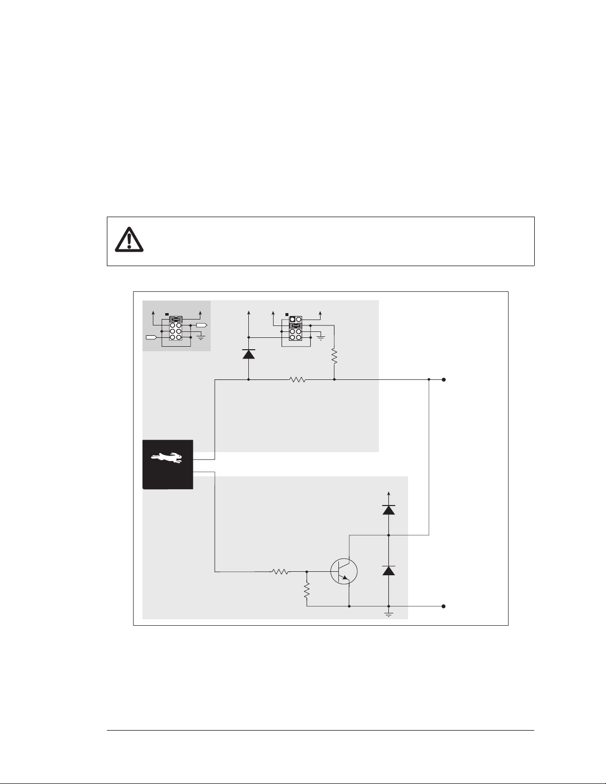
3.2 Digital I/O
100 kW
27 kW
+5 V
+Kx
SINKING
OUTPUT
27 kW
470 W
DIGITAL
INPUT
DIO0DIO31
Factory
Default
setting
+Kx
GND
+3.3 V
Sinking Output
setting
+5 V
+Kx
Rabbit® RIO
3.2.1 Configurable I/O
3.2.1.1 Digital Inputs
The BL4S200 has 32 configurable I/O, DIO0–DIO31, each of which may be configured
individually in software as either digital inputs or as sinking digital outputs. By default, a
configurable I/O channel is a digital input, but may be set as a sinking digital output by
using the setDigOut() function call. The inputs are factory-configured to be pulled up
to +5 V, but they can also be pulled up to +K or DCIN, or pulled down to 0 V in banks by
changing a jumper as shown in Figure 7.
CAUTION: Do not simultaneously jumper more than one setting on a particular
jumper header (JP9, JP8, JP1, and JP2) when configuring a bank of configurable I/O.
BL4S200 User’s Manual 27
Figure 7. BL4S200 Configurable I/O DIO0–DIO31
Page 28
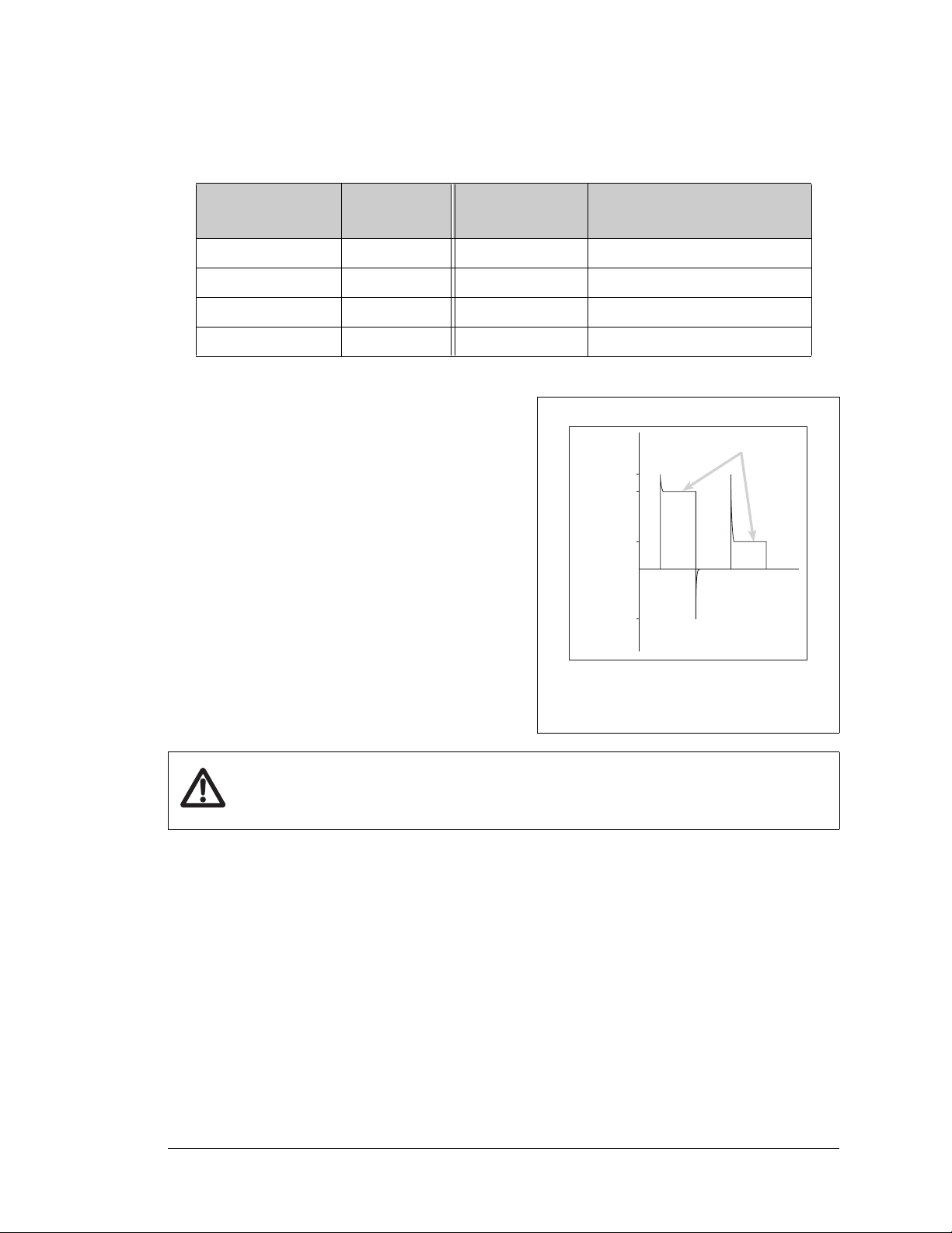
Table 3 lists the banks of configurable I/O and summarizes the jumper settings.
+40 V
+36 V
+3.3 V
5 V
Normal Switching
Levels
Spikes
Digital Input Voltage
Spikes
Spikes
Table 3. Banks of BL4S200 Digital Inputs
Digital Inputs
Configuration
Header
Pins Jumpered Pulled Up/Pulled Down
DIO0–DIO7 JP9 1–2 Inputs pulled up to +Kx
DIO8–DIO15 JP8 3–4 Inputs pulled up to +5 V
DIO16–DIO23 JP1 5–6 Inputs pulled down to GND
DIO24–DIO31 JP2 7–8 Inputs pulled up to + 3.3 V
The actual switching threshold is approximately
1.40 V. Anything below this value is a logic 0,
and anything above 1.90 V is a logic 1. The configurable I/O are each fully protected over a
range of 0 V to +36 V, and can handle short
spikes from -5 V to +40 V.
NOTE: If the inputs are pulled up to +Kx, the
voltage range over which the digital inputs
are protected changes to 5 V - Kx to +36 V.
Figure 8. BL4S200 Digital Input
Protected Range
CAUTION: Do not allow the voltage on a configurable I/O pin to exceed +Kx to
avoid damaging the input.
BL4S200 User’s Manual 28
Page 29
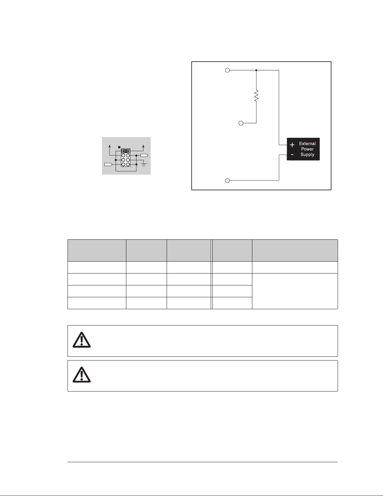
3.2.1.2 Sinking Digital Outputs
Sinking Output
setting
+5 V
+Kx
DIO0DIO31
LOAD
(200 mA
max.)
+Kx
GND
When you configure a configurable I/O
pin as a sinking output, be sure to connect an external voltage source up to
36 V DC across the corresponding
+Kx and GND on connector J1, J2, J9,
or J10, and set the pullup jumper on
the corresponding JP1/JP2/JP8/JP9
header to +Kx.
Table 4 lists the banks of configurable
I/O and the corresponding +Kx.
Figure 9. Load and +K Power Supply
Connections for Sinking Digital Output
Table 4. BL4S200 Sinking Outputs
Digital Inputs +Kx
DIO0–DIO7 KA on J10 JP9 1–2 I/O pulled up to +Kx
DIO8–DIO15 KB on J9 JP8 3–4
DIO16–DIO23 KC on J1 JP1 5–6
DIO24–DIO31 KD on J2 JP2 7–8
Configuration
Header
Pins
Jumpered
Pulled Up/Pulled Down
Do not use these options for a
sinking output.
CAUTION: Do not simultaneously jumper more than one setting on a particular
jumper header (JP9, JP8, JP1, and JP2) when configuring a bank of configurable I/O.
CAUTION: Do not allow the voltage on a configurable I/O pin to exceed +Kx to
avoid damaging the input.
BL4S200 User’s Manual 29
Page 30

3.2.1.3 Configurable I/O Special Uses
Individual configurable I/O pins may be used for interrupts, input capture, as quadrature
decoders, or as PWM outputs. The use of these channels for PWM, interrupts, input capture, and as quadrature decoders is described in the Rabbit RIO User’s Manual.
Blocks of configurable I/O pins are associated with counters/timers on the three Rabbit RIO
chips that support them. Table 5 provides complete details for these associations.
Table 5. Counter/Timer Associations for BL4S200 Configurable I/O Pins
Configurable I/O
Pin(s)
DIO0–DIO3
DIO4–DIO7
DIO8–DIO11
DIO12–DIO15
DIO16–DIO17 0 (I/O) 2 (U9)
DIO18–DIO19 1 (I/O) 2 (U9)
DIO20–DIO21 2 (I/O) 2 (U9)
DIO22–DIO23 3 (I/O) 2 (U9)
DIO24–DIO25 4 (I/O) 2 (U9)
DIO26–DIO27 5 (I/O) 2 (U9)
DIO28
Counter/Timer
Blocks
4 (outputs)
5 (inputs)
0 (outputs)
1 (inputs)
2 (outputs)
3 (inputs)
4 (outputs)
5 (inputs)
6 (output)
7 (input)
RIO Chip Index
0 (U8)
1 (U7)
1 (U7)
1 (U7)
0 (U8)
DIO29
DIO30 6 (input only) 2 (U9)
DIO31 7 (input only) 2 (U9)
6 (output)
7 (input)
1 (U7)
Configurable I/O pins DIO30 and DIO31 fully support all input-associated special uses
such as interrupts and input captures, but otherwise they are limited to function only as
regular digital I/O pins because their outputs are latch-driven since sufficient Rabbit RIO
resources are not available to support their use for specialized outputs.
Appendix D provides further details on the blocks and pins associated with each Rabbit
RIO chip to facilitate configuring each block consistently and to identify misconfigured
pins when a software function call returns a Mode Conflict error code.
BL4S200 User’s Manual 30
Page 31

Keep the following guidelines in mind when selecting special uses for the remaining configurable I/O pins.
• Interrupts, event counters, and input capture are available on any configurable I/O pin.
• Each Quadrature Decoder channel requires at least two configurable I/O pins associ-
ated with the same counter/timer block; three configurable I/O pins associated with the
same counter/timer block are needed if you need indexing.
• When using configurable I/O pins for PWM outputs, they can only share the same RIO
block if they are using the same period or frequency. Depending on the pin(s) selected,
from one to four PWM outputs could operate based on the same counter block.
Remember to set the corresponding jumper (Table 4) so that the I/O for that bank are
pulled up to the selected voltage. The output voltage swing will be from 0 to the voltage
you selected\.
The sample program PWM.C in the DIO subdirectory in SAMPLES\BLxS2xx shows
how to set up and use the PWM outputs.
• Configurable I/O have their own set of function calls. These function calls will only
work with configurable I/O. High-current outputs have their own function calls that end
with _H.
See Appendix D for additional information about the Rabbit RIO pin associations and
how to select which special functionality to best apply to a particular pin.
BL4S200 User’s Manual 31
Page 32

Interrupt, Counter, and Event Capture Setup
Channel 0
Begin
Count
End
Count
Channel 1
Start
Event
End
Event
External interrupts on the BL4S200 configurable I/O pins are configured using the
setExtInterrupt() function call. The interrupt can be set up to occur on a rising edge,
a falling edge, or either edge.
An input channel may be set up to count
events, with the count incrementing or
decrementing, using the rising edge, falling edge, or either edge as triggers to start/
end the count. This feature is configured
using the setCounter() function call.
A more extensive use of the timing abilities
of the BL4S200 configurable I/O can be
realized through the event capture function
call, setCapture(). Here the count of a
particular clock cycle is noted at the start of
the event and at the end of the event so that
the time between them can be determined.
This can be set up on one or two configurable I/O channels. The event counter can
be reset with the resetCounter() function call.
The counter readings can be obtained via the
getBegin() or getEnd() function calls.
BL4S200 User’s Manual 32
Page 33

PWM/PPM Outputs Setup
Period
Duty
Cycle
Inverted
Noninverted
PWM
OUTPUT
Period
Duty
Cycle
Shifted
PPM
OUTPUT
Offset
A PWM output is described as noninverted
when it starts high, remains high for a duty
cycle that is a fraction of the period, then
goes low for the remainder of the period.
Similarly, an inverted PWM output starts
low, remains low for a duty cycle that is a
fraction of the period, then goes high for
the remainder of the period.
A PWM output is normally set up to start
when triggered by an event, and may be
set up so that the leading and trailing edges
of several PWM outputs are aligned as
long as the all the PWM outputs are on the
same block of a particular Rabbit RIO
chip.
A PPM ouput is similar to a PWM output,
except it is shifted by an offset relative to
the event that triggered the start of the
PPM output.
A PPM output is either inverted or noninverted, based on whether it starts high or
low, and may be set up so that their leading and trailing edges of several PPM outputs are aligned as long as the all the PPM
outputs are on the same block of a particular Rabbit RIO chip
PWM and PPM outputs on the BL4S200 configurable I/O are configured using the set-
PWM()
rent outputs are configured using the
and setPPM() function calls. PWM and PPM outputs on the BL4S200 high-cur-
setPWM_H() and setPPM_H() function calls.
BL4S200 User’s Manual 33
Page 34

3.2.2 High-Current Digital Outputs
+Ka
+Kb
LOAD
A
A
B
B
The BL4S200 has eight high-current digital outputs, HOUT0–HOUT7, which can each
sink or source up to 2 A. Figure 10 shows a wiring diagram for using the digital outputs in
either a sinking or a sourcing configuration.
Figure 10. BL4S200 High-Current Outputs
All the digital outputs sink and source actively. They can be used as high-side drivers, lowside drivers, or as an H-bridge driver. When the BL4S200 is first powered up or reset, all
the outputs are disabled, that is, at a high-impedance tristate.
Each bank of four high-current output has its own +K supply, as shown in Table 6. When
wiring the high-current outputs, keep the distance to the power supply as short as possible.
Table 6. BL4S200 High-Current Outputs
High-Current Outputs +Kx Connector
HOUT0–HOUT3 K1 J3
HOUT4–HOUT7 K2 J4
For the H bridge, which is shown in Figure 11,
Ka and Kb should be the same. This is most
easily accomplished by using outputs from the
same bank on one connector.
Figure 11. H Bridge
BL4S200 User’s Manual 34
Page 35

High-current outputs have their own function calls for control (digOut_H() and
digOutTriState_H()) and to set up the PWM and PPM outputs. All function calls that
work with high-current outputs end with _H — do not confuse these function calls with
their configurable I/O counterparts. The digOutConfig_H() function call configures the
high-current outputs as two state outputs with either sinking or sourcing drivers. The
digOutTriStateConfig_H() function call configures the high-current outputs as
tristate drivers with both sinking and sourcing capability.
BL4S200 User’s Manual 35
Page 36

3.3 Serial Communication
The BL4S200 has up to three serial communication ports, one RS-485 channel, and either
one RS-232 serial channel (with RTS/CTS) or two RS-232 (3-wire) channels. Table 7
summarizes the serial ports.
Table 7. Serial Communication Configurations
BL4S200
Model
BL4S200 — RS-485
BL4S210 RS-232 RS-485 — —
BL5S220 — RS-485
BL4S230 — RS-485
B C E F
Serial Port
(PD6/PD7)
(PD6/PD7)
(PD6/PD7)
RS-232
RS-232
RS-232
RS-232
(PD2/PD3)
RS-232
(PD2/PD3)
RS-232
(PD2/PD3)
Two RabbitNet™ expansion ports are multiplexed from Serial Port D. The BL4S200 also
has one CMOS serial channel that serves as the programming port.
All three serial ports operate in an asynchronous mode. An asynchronous port can handle
7 or 8 data bits. A 9th bit address scheme, where an additional bit is sent to mark the first
byte of a message, is also supported. Serial Port A, the programming port, can be operated
alternately in the clocked serial mode. In this mode, a clock line synchronously clocks the
data in or out. Either of the two communicating devices can supply the clock. The BL4S200
boards supports standard asynchronous baud rates from 3.7 Mbps to 9.2 Mbps, depending
on the frequency the Rabbit microprocessor on a particular model is operating at.
3.3.1 RS-232
The BL4S200 RS-232 serial communication is supported by an RS-232 transceiver. This
transceiver provides the voltage output, slew rate, and input voltage immunity required to
meet the RS-232 serial communication protocol. Basically, the chip translates the Rabbit
microprocessor’s CMOS signals to RS-232 signal levels. Note that the polarity is reversed
in an RS-232 circuit so that a +3.3 V output becomes approximately -10 V and 0 V is output as +10 V. The RS-232 transceiver also provides the proper line loading for reliable
communication.
RS-232 can be used effectively at the BL4S200’s maximum baud rate for distances of up
to 15 m.
3.3.2 RS-485
The BL4S200 has one two-wire RS-485 serial channel, which is connected to Serial Port C
through an RS-485 transceiver. This port operates in a half-duplex communication mode,
which requires directional control on the communication line.
BL4S200 User’s Manual 36
Page 37

The BL4S200 can be used in an RS-485 multidrop network. Connect the 485+ to 485+
RS-485
RS485+
GND
RS-485
RS485+
GND
RS-485
RS485+
GND
RESET
S1
S2
R1
CORE +3.3 V
DS1
DS2
J9
J10
J11
J12
J8
J7
J6
J5
J4
J3
J2
J1
RCM1
R7
R8
R9
R10
C63
JP4
JP5
JP6
JP3
C62
C47
JP7
RS485
JP9
JP8
KB
+5 V
GND
+3.3 v
KA
+5 V
GND
+3.3 V
C52
C55
C57
C61
C56
C60
C50
C51
C49
C59
C54
C48
C53
C58
U7
C38
C39
C40
C21
C27
C33
C17
C19
C25
C14
R4
R2
C12
C13 U5
U6
C16
C41
C42
C43
C23
C29
C35
C22
C28
C34
U8
C44
C45
C46
C24
C30
C36
R117
RP1
U4
C37
RP2
R5
R121
L2 L3
BT1
C31
C32
U3
C15
C10
U2
C11
C9
C8
U1
R116
R3
R118
C18
C20
C26
JP1
JP2
D2
D3
L1
D4
C1
C2
C3
C4
C6
TERM
TERM
KC
+5 V
GND
+3.3 V
KD
+5 V
GND
+3.3 V
CAUTION! HOT!
CAUTION! HOT!
D6 D5 D8 D7
D9
C5
C7
D10
DS4
DS3
R6
BOARD
+3.3 V
POWER
IN
RNET PWR
4
1
7
14
8
R13
R12
R11
6
10
5
6
10
5
6
10
5
2
4
3
6
10
5
D1
6
10
5
6
10
5
610
5
Battery
D56
D57
D58
D59
D60
J1
R1
R2
R19
R3
R4
C3
L1
C1
C2
Y1
4
1
3
R16
R17
C4
C8
C5
C6
C7
R20
U2
R21
R22
R23
C13
C12
L2
C10
JP15
C21
U7
R38
J2
R37
R36
C22
DS1
LINK
SPEED
FDX
DS3
DS2
R39
R40
R41
R35
C23
R34
U6
R33
R31
R32
D1
R66
C14
C11
C9
R7
R6
DS4
R42
J3
U18
R65
R67
R64
R29
R68
R69
R30
R24
C15 C16 R28 R27 R26
R25
C20
U5
JP12
JP13
JP14
R71
R70
R5
JP1
JP2
R72
JP3
JP4
JP5
JP6
JP7
JP8
JP9
JP10
JP11
U3
R8
R9
Q2
Q3
C91
C93
U1
R10
R11
R13
R12
R14
R15
C17
C18
C19
C92
C90
JP7
4
3
2
1
R12
681 W
R11
220 W
R13
681 W
485+
485
6
7
termi-
nation
bias
bias
U23
JP7
2
1
6
5
6
5
Factory
Default
and 485– to 485– using single twisted-pair wires (nonstranded, tinned) as shown in
Figure 12. Note that a common ground is recommended.
Figure 12. BL4S200 Multidrop Network
The BL4S200 comes with a 220 termination resistor and two 681 bias resistors
installed and enabled with jumpers across pins 1–2 and 5–6 on header JP7, as shown in
Figure 13.
Figure 13. RS-485 Termination and Bias Resistors
BL4S200 User’s Manual 37
Page 38

For best performance, the bias and termination resistors in a multidrop network should
only be enabled on both end nodes of the network. Disable the termination and bias resistors on any intervening BL4S200 units in the network by removing both jumpers from
header JP6.
TIP: Save the jumpers for possible future use by “parking” them across pins 1–3 and 4–6
of header JP7. Pins 3 and 4 are not otherwise connected to the BL4S200.
3.3.3 Programming Port
The RabbitCore module on the BL4S200 has a 10-pin programming header. The programming port uses the Rabbit 4000 or Rabbit 5000 Serial Port A for communication, and is
used for the following operations.
• Programming/debugging
• Cloning
The programming port is used to start the BL4S200 in a mode where the BL4S200 will
download a program from the port and then execute the program. The programming port
transmits information to and from a PC while a program is being debugged.
The Rabbit 4000 or Rabbit 5000 startup-mode pins (SMODE0, SMODE1) are presented
to the programming port so that an externally connected device can force the BL4S200 to
start up in an external bootstrap mode. The BL4S200 can be reset from the programming
port via the /EXT_RSTIN line.
The Rabbit microprocessor status pin is also presented to the programming port. The status
pin is an output that can be used to send a general digital signal.
NOTE: Refer to the Rabbit 4000 Microprocessor User’s Manual and the Rabbit 5000
Microprocessor User’s Manual for more information related to the bootstrap mode.
BL4S200 User’s Manual 38
Page 39

3.3.4 Ethernet Port
ETHERNET
RJ-45 Plug
1. E_Tx+
2. E_Tx
3. E_Rx+
6. E_Rx
1
8
RJ-45 Jack
Figure 14 shows the pinout for the Ethernet port (J2 on the BL4S200 modules that support
Ethernet networking). Note that there are two standards for numbering the pins on this connector—the convention used here, and numbering in reverse to that shown. Regardless of
the numbering convention followed, the pin positions relative to the spring tab position
(located at the bottom of the RJ-45 jack in Figure 14) are always absolute, and the RJ-45
connector will work properly with off-the-shelf Ethernet cables.
Figure 14. RJ-45 Ethernet Port Pinout
Three LEDs are placed next to the RJ-45 Ethernet jack on the BL4S200 model, one to
indicate Ethernet link/activity (LINK/ACT), one to indicate when the BL4S200 is connected to a functioning 100Base-T network (SPEED), and one (FDX/COL) to indicate that
the current connection is in full-duplex mode (steady on) or that a half-duplex connection
is experiencing collisions (blinks).
Two LEDs are placed next to the RJ-45 Ethernet jack on the BL4S210 model, one to indicate an Ethernet link (LNK) and one to indicate Ethernet activity (ACT).
The RJ-45 connector is shielded to minimize EMI effects to/from the Ethernet signals.
BL4S200 User’s Manual 39
Page 40

3.4 A/D Converter Inputs
ADC
953 kW
10 pF
AIN0
AGND
AIN1
10 pF
Ref. Voltage
from D/A Converter
105 kW
105 kW
953 kW
The single A/D converter chip used in the BL4S200 has a resolution of 12 bits (11 bits for
the value and one bit for the polarity)
fier. Each external input has circuitry that provides scaling and filtering. All 8 external
inputs are scaled and filtered to provide the user with an input impedance of 1 M and a
variety of single-ended unipolar, single-ended bipolar, and differential bipolar ranges as
shown in Table 8.
Figure 15 shows a pair of A/D converter input circuits. The resistors form an approx. 10:1
attenuator, and the capacitors filter noise pulses from the A/D converter inputs.
. The A/D converter chip has a programmable ampli-
Figure 15. Buffered A/D Converter Inputs
The A/D converter chip can only accept positive voltages. By pairing the analog inputs and
setting the reference voltage from the D/A converter, single-ended unipolar, single-ended
bipolar, differential bipolar, or current (4–20 mA on channels 0–3 only) measurements are
possible, and can be configured for each channel or channel pair with the
ter in the anaInConfig() software function call. Adjacent A/D converter inputs AIN4–
AIN7are paired to make bipolar measurements. The available voltage ranges are listed in
opmode parame-
Table 8.
BL4S200 User’s Manual 40
Page 41

Table 8. A/D Converter Input Voltage Ranges
100 W
JP4
AIN0
AIN1
AIN2
AIN3
Example of
adding your
own resistor
Do not jumper
JP4 in this case
Apply jumpers
for factory-default
current measurements
Amplifier
Voltage R a n g e
Gain
Single-Ended
Unipolar
Single-Ended
Bipolar
Differential
Bipolar
1 0–20 V ±10 V ± 20 V
2 0–10 V ±5 V ± 10 V
4 0–5 V ±2.5 V ± 5 V
5 0–4 V ±2 V ± 4 V
*
8
0–2.5 V ±1.25 V ± 2.5 V
10 0–2 V ±1 V ± 2 V
16 0–1.25 V ±0.625 V ± 1.25 V
20 0–1 V ±0.5 V ± 1 V
* 4–20 mA operation is available with an amplifier gain of 8
In the differential mode, each individual channel is limited to half the total voltage—for
example, the range for a gain code of 1 is ±20 V, but each channel is limited to ±10 V.
When using channels AIN0–AIN3 for current
measurements, remember to set the corresponding jumper(s) on header JP4. The current
measurements are realized by actually measuring the voltage drop across a 100 resistor.
You may substitute a different resistor value as
shown in Figure 16.
Figure 16. Analog Current Measurements
CAUTION: If you are using a supply voltage of +10 V DC for the 4–20 mA current
measurements, do not exceed 500 for these resistors.
The A/D converter inputs are factory-calibrated, and the calibration constants are stored in
the user block.
When you start to develop your application, run USERBLOCK_READ_WRITE.C in the
SAMPLES\UserBlock folder to save the factory calibration constants in case you inad-
vertently write over them while running the sample programs.
BL4S200 User’s Manual 41
Page 42

3.4.1 A/D Converter Calibration
To get the best results form the A/D converter, it is necessary to calibrate each mode
(single-ended, differential, and current) for each of its gains. It is imperative that you calibrate each of the A/D converter inputs in the same manner as they are to be used in the
application. For example, if you will be performing floating differential measurements or
differential measurements using a common analog ground, then calibrate the A/D converter in the corresponding manner. The calibration table in software only holds calibration constants based on mode, channel, and gain. Other factors affecting the calibration must
be taken into account by calibrating using the same mode and gain setup as in the intended use.
Sample programs are provided to illustrate how to read and calibrate the various A/D
inputs for the three operating modes.
Mode Read Calibrate
Single-Ended, unipolar AD_RD_SE_UNIPOLAR.C ADC_CAL_SE_UNIPOLAR.C
Single-Ended, bipolar AD_RD_SE_BIPOLAR.C ADC_CAL_SE_BIPOLAR.C
Differential, bipolar AD_RD_DIFF.C ADC_CAL_DIFF.C
Milli-Amp AD_RD_MA.C ADC_CAL_MA.C
These sample programs are found in the ADC subdirectory in SAMPLES\BLxS2xx. See
Section 4.2.3 for more information on these sample programs and how to use them.
BL4S200 User’s Manual 42
Page 43

3.5 D/A Converter Outputs
44.2 kW
10 kW
AOUT0
AGND
1.95 V ref.
1.116 V ref.
10 kW
AOUT1
3.00 V ref.
158 kW
158 kW
11 kW
11 kW
AOUT0
AOUT1
DAC
Voltage
Outputs
Current
Outputs
0.01 µF
12 V
-12 V
10 pF
44.2 kW
JP3
10 W
10 W
The two D/A converter outputs are buffered and scaled to provide an output from 0 V to
+10 V (12-bit resolution) or ±10 V (11-bit resolution, one bit used for polarity). The selection is made via jumpers on header JP3 for AOUT0 and via JP6 for AOUT1. There is also
the option to select either D/A converter output as a 4–20 mA current output via jumpers
on header JP5. Figure 17 shows the D/A converter outputs.
Figure 17. D/A Converter Outputs
Table 9 summarizes the jumper settings to configure each D/A converter output. Note that
the software configuration requires both channels to be configured the same way.
Table 9. D/A Converter Jumper Configurations
D/A Converter Output JP3 JP5 JP6
AOUT0
AOUT1
BL4S200 User’s Manual 43
0 to +10 V (default)
1–2
3–4
1–3 —
±10 V 5–6 1–3 —
4–20 mA — 3–5 —
0 to +10 V (default) — 2–4
±10 V — 2–4 5–6
4–20 mA — 4–6 —
1–2
3–4
Page 44

To stay within the maximum power dissipation of the D/A converter circuit, the maximum
D/A converter output current is 10 mA per channel for the voltage outputs. If you are
using the current outputs, keep the resistance driven by a current output channel above
1k to stay within the voltage compliance capability of the op-amp output circuit.
As Figure 17 shows, both the voltage and the current outputs for a particular channel are
driven by the same output on the D/A converter chip. As a result, either the anaOut-
Volts()
or the anaOutmAmps() function calls will set both the voltage and the current
outputs corresponding to a particular channel. Pay attention to which function call you use
to set the D/A converter output — setting a current level using voltage function calls will
not produce a correctly calibrated output.
The D/A converter outputs are factory-calibrated and the calibration constants are stored in
the user block.
3.5.1 D/A Converter Calibration
To get the best results form the D/A converter, it is necessary to calibrate each mode (unipolar, bipolar, and current) that you intend to use. It is imperative that you calibrate each
of the D/A converter outputs in the same manner as they are to be used in the application.
The calibration table in software only holds calibration constants based on unipolar, bipolar, and voltage or current operation. Other factors affecting the calibration must be taken into
account by calibrating using the same mode and voltage/current setup as in the intended use.
Sample programs are provided to illustrate how to calibrate the various D/A outputs for
the three operating modes.
Mode Calibrate
Vo l t a g e DAC_CAL_VOLTS.C
Current DAC_CAL_MA.C
These sample programs are found in the
DAC subdirectory in SAMPLES\BLxS2xx. See
Section 4.2.4 for more information on these sample programs and how to use them.
BL4S200 User’s Manual 44
Page 45

3.6 Analog Reference Voltages Circuit
3.32 kW
1.95 V
3.00 V
+2.5 V
6
5
20 kW
100 kW
11.8 kW
0.1 µF
12.4 kW
1.116 V
10 kW
0.1 µF
12
13
10
9
U21
U21
U21
Figure 18 shows the analog voltage reference circuit.
Figure 18. Analog Reference Voltages
The A/D converter chip supplies the 2.5 V reference voltage, which is then amplified and
buffered to provide the 3.00 V, 1.95 V, and 1.116 V reference voltages used by the digital
output circuits.
The D/A converter chip provides the reference voltages for the digital inputs to provide
single-ended unipolar or differential measurements [0 V], or to provide single-ended bipolar
measurements [V = (voltage range) ÷ 9]. Because the D/A converter chip operation is configured by the
function before running anaInConfig() if you plan to use the analog outputs to ensure
that the reference voltages are established first before the analog inputs are configured.
BL4S200 User’s Manual 45
anaOutConfig() function, it is important to run the anaOutConfig()
Page 46

3.7 USB Programming Cable
Power
RESET BL4S200 when changing mode:
Cycle power off/on or press RESET
after removing or attaching programming cable.
Program Mode
RESET
S1
S2
R1
CORE +3.3 V
DS1
DS2
J9
J10
J11
J12
J8
J7
J6
J5
J4
J3
J2
J1
RCM1
R7
R8
R9
R10
C63
JP4
JP5
JP6
JP3
C62
C47
JP7
RS485
JP9
JP8
KB
+5 V
GND
+3.3 v
KA
+5 V
GND
+3.3 V
C52
C55
C57
C61
C56
C60
C50
C51
C49
C59
C54
C48
C53
C58
U7
C38
C39
C40
C21
C27
C33
C17
C19
C25
C14
R4
R2
C12
C13 U5
U6
C16
C41
C42
C43
C23
C29
C35
C22
C28
C34
U8
C44
C45
C46
C24
C30
C36
R117
RP1
U4
C37
RP2
R5
R121
L2 L3
BT1
C31
C32
U3
C15
C10
U2
C11
C9
C8
U1
R116
R3
R118
C18
C20
C26
JP1
JP2
D2
D3
L1
D4
C1
C2
C3
C4
C6
TERM
TERM
KC
+5 V
GND
+3.3 V
KD
+5 V
GND
+3.3 V
CAUTION! HOT!
CAUTION! HOT!
D6 D5 D8 D7
D9
C5
C7
D10
DS4
DS3
R6
BOARD
+3.3 V
POWER
IN
RNET PWR
4
1
7
14
8
R13
R12
R11
6
10
5
6
10
5
6
10
5
2
4
3
6
10
5
D1
6
10
5
6
10
5
610
5
Battery
D56
D57
D58
D59
D60
Run Mode
J1
R1
R2
R19
R3
R4
C3
L1
C1
C2
Y1
4
1
3
R16
R17
C4
C8
C5
C6
C7
R20
U2
R21
R22
R23
C13
C12
L2
C10
JP15
C21
U7
R38
J2
R37
R36
C22
DS1
LINK
SPEED
FDX
DS3
DS2
R39
R40
R41
R35
C23
R34
U6
R33
R31
R32
D1
R66
C14
C11
C9
R7
R6
DS4
R42
J3
U18
R65
R67
R64
R29
R68
R69
R30
R24
C15 C16 R28 R27 R26
R25
C20
U5
JP12
JP13
JP14
R71
R70
R5
JP1
JP2
R72
JP3
JP4
JP5
JP6
JP7
JP8
JP9
JP10
JP11
U3
R8
R9
Q2
Q3
C91
C93
U1
R10
R11
R13
R12
R14
R15
C17
C18
C19
C92
C90
RESET
Colored
edge
To
PC USB port
PROG
DIAG
Programming
Cable
PROG
DIAG
The USB programming cable is used to connect the serial programming port of the
BL4S200 to a PC USB port. The programming cable converts the voltage levels used by
the PC USB port to the CMOS voltage levels used by the Rabbit microprocessor.
When the PROG connector on the programming cable is connected to the programming
header on the BL4S200’s RabbitCore module, programs can be downloaded and
debugged over the serial interface.
The DIAG connector of the programming cable may be used on the programming header on
the BL4S200’s RabbitCore module with the BL4S200 operating in the Run Mode. This
allows the programming port to be used as a regular serial port.
3.7.1 Changing Between Program Mode and Run Mode
The BL4S200 is automatically in Program Mode when the PROG connector on the programming cable is attached, and is automatically in Run Mode when no programming cable
is attached. When the Rabbit microprocessor is reset, the operating mode is determined by
the status of the SMODE pins. When the programming cable’s PROG connector is attached,
the SMODE pins are pulled high, placing the Rabbit microprocessor in the Program Mode.
When the programming cable’s PROG connector is not attached, the SMODE pins are
pulled low, causing the Rabbit microprocessor to operate in the Run Mode.
A program “runs” in either mode, but can only be downloaded and debugged when the
BL4S200 is in the Program Mode.
Refer to the
User’s Manual
Rabbit 4000 Microprocessor User’s Manual and the Rabbit 5000 Microprocessor
Figure 19. BL4S200 Program Mode and Run Mode Setup
for more information on the programming port and the programming cable.
BL4S200 User’s Manual 46
Page 47

3.8 Other Hardware
3.8.1 Clock Doubler
The BL4S200 Ethernet models and the Wi-Fi model (BL4S200, BL4S210, and BL5S220)
take advantage of the Rabbit microprocessor’s internal clock doubler. A built-in clock
doubler allows half-frequency crystals to be used to reduce radiated emissions. The clock
doubler on the BL4S230 is disabled by default.
The clock doubler may be disabled on the BL4S200 Ethernet models (BL4S200 and
BL4S210)if the higher clock speeds are not required. Disabling the clock doubler will
reduce power consumption and further reduce radiated emissions. The clock doubler is
disabled with a simple configuration macro as shown below.
1. Select the “Defines” tab from the Dynamic C Options > Project Options menu.
2. Add the line CLOCK_DOUBLED=0 to always disable the clock doubler.
The clock doubler is enabled by default, and usually no entry is needed. If you need to
specify that the clock doubler is always enabled, add the line CLOCK_DOUBLED=1 to
always enable the clock doubler.
3. Click OK to save the macro. The clock doubler will now remain off whenever you are
in the project file where you defined the macro.
NOTE: Do not disable the clock doubler on the Wi-Fi model (BL5S220) since Wi-Fi
operations depend highly on the CPU resources.
BL4S200 User’s Manual 47
Page 48

3.8.2 Spectrum Spreader
The Rabbit microprocessors features a spectrum spreader, which help to mitigate EMI
problems. By default, the spectrum spreader is on automatically, but it may also be turned
off or set to a stronger setting. The means for doing so is through a simple configuration
macro as shown below.
1. Select the “Defines” tab from the Dynamic C Options > Project Options menu.
2. Normal spreading is the default, and usually no entry is needed. If you need to specify normal spreading, add the line
ENABLE_SPREADER=1
For strong spreading, add the line
ENABLE_SPREADER=2
To disable the spectrum spreader, add the line
ENABLE_SPREADER=0
NOTE: The strong spectrum-spreading setting is not recommended since it may limit
the maximum clock speed or the maximum baud rate. It is unlikely that the strong setting will be used in a real application.
3. Click OK to save the macro. The spectrum spreader will be set according to the macro
value whenever a program is compiled using this project file.
NOTE: Refer to the Rabbit 4000 Microprocessor User’s Manual and the Rabbit 5000
Microprocessor User’s Manual for more information on the spectrum-spreading set-
tings and the maximum clock speed.
BL4S200 User’s Manual 48
Page 49

3.9 Memory
3.9.1 SRAM
The RabbitCore modules used with the BL4S200 boards all have 512 KB of data SRAM.
The RabbitCore modules on the BL4S200 and BL5S220 boards also have 512 KB and
1 MB of fast program execution SRAM.
3.9.2 Flash Memory
The RabbitCore modules used with the BL4S200 boards have 512 KB or 1 MB of flash
memory.
NOTE: Rabbit recommends that any customer applications should not be constrained by
the sector size of the flash memory since it may be necessary to change the sector size
in the future.
Writing to arbitrary flash memory addresses at run time is also discouraged. Instead,
define a “user block” area to store persistent data. The functions writeUserBlock()
and readUserBlock() are provided for this.
3.9.3 VBAT RAM Memory
The tamper detection feature of the Rabbit microprocessor can be used to detect any
attempt to enter the bootstrap mode. When such an attempt is detected, the VBAT RAM
memory in the Rabbit microprocessor is erased. The serial bootloader on the RabbitCore
module on the BL4S200 model uses the bootstrap mode to load the SRAM, which erases
the VBAT RAM memory on any reset, and so it cannot be used on this model for tamper
detection.
3.9.4 microSD™ Cards
The RabbitCore module on the BL4S200 model supports a removable microSD™ Card up
to 1 GB to store data and Web pages. The microSD™ Card is particularly suitable for
mass-storage applications, but is generally unsuitable for direct program execution.
Unlike other flash devices, the microSD™ Card has some intelligence, which facilitates
working with it. You do not have to worry about erased pages. All microSD™ Cards sup-
port 512-byte reads and writes, and handle any necessary pre-erasing internally.
Figure 20 shows how to insert or remove the microSD™ Card. The card is designed to fit
easily only one way — do not bend the card or force it into the slot. While you remove or
insert the card, take care to avoid touching the electrical contacts on the bottom of the card
to prevent electrostatic discharge damage to the card and to keep any moisture or other
contaminants off the contacts. You will sense a soft click once the card is completely
inserted. To remove it, gently press the card towards the middle of the RabbitCore module
on the BL4S200 model — you will sense a soft click and the card will be ready to be
removed. Do not attempt to pull the card from the socket before pressing it in — otherwise
the ejection mechanism will get damaged. The ejection mechanism is spring-loaded, and
will partially eject the card when used correctly.
BL4S200 User’s Manual 49
Page 50

Figure 20. Insertion/Removal of microSD Card
J1
R1
R2
R19
R3
R4
C3
L1
C1
C2
Y1
4
1
3
R16
R17
C4
C8
C5
C6
C7
R20
U2
R21
R22
R23
C13
C12
L2
C10
JP15
C21
U7
R38
J2
R37
R36
C22
DS1
LINK
SPEED
FDX
DS3
DS2
R39
R40
R41
R35
C23
R34
U6
R33
R31
R32
D1
R66
C14
C11
C9
R7
R6
DS4
R42
J3
U18
R65
R67
R64
R29
R68
R69
R30
R24
C15 C16 R28 R27 R26
R25
C20
U5
JP12
JP13
JP14
R71
R70
R5
JP1
JP2
R72
JP3
JP4
JP5
JP6
JP7
JP8
JP9
JP10
JP11
U3
R8
R9
Q2
Q3
C91
C93
U1
R10
R11
R13
R12
R14
R15
C17
C18
C19
C92
C90
NOTE: When using the Dynamic C FAT file system, do not remove or insert the
microSD™ Card while LED DS4 above the
microSD™ Card is on to indicate that the
microSD™ Card is mounted. The LED will go off when the microSD™ Card is
unmounted, indicating that it is safe to remove it.
Rabbit recommends that you use the microSD™ Card holder at connector J3 on the Rab-
bitCore module only for the microSD™ Card since other devices are not supported. Be
careful to remove and insert the card as shown, and be careful not to insert any foreign
objects, which may short out the contacts and lead to the destruction of your card.
It is possible to hot-swap microSD™ Cards without removing power from the BL4S200.
The file system must be closed before the cards can be hot-swapped. The chip selects
associated with the card must be set to their inactive state, and read/write operations
addressed to the microSD™ Card port cannot be allowed to occur. These operations can
be initiated in software by sensing an external switch actuated by the user, and the card
can then be removed and replaced with a different one. Once the application program
detects a new card, the file system can be opened. These steps allow the microSD™ Card
to be installed or removed without affecting either the program, which continues to run on
the RCM4300 module, or the data stored on the card. The Dynamic C FAT file system will
handle this overhead automatically when you unmount the microSD™ Card. LED DS4
above the microSD™ Card is used by the FAT file system to show when the media is
mounted.
Standard Windows SD Card readers may be used to read the microSD™ Card formatted
by the Dynamic C FAT file system with the BL4S200 as long as it has not been partitioned. SD Card adapters have a sliding switch along the left side that may be moved
down to write-protect the microSD™ Card while it is being used with an SD Card reader.
Sample programs in the
microSD™ Cards.
BL4S200 User’s Manual 50
SAMPLES\BLxS2xx\SD_Flash folder illustrate the use of the
Page 51

4. SOFTWARE
Dynamic C is an integrated development system for writing
embedded software. It runs on an IBM-compatible PC and is
designed for use with single-board computers and other devices
based on the Rabbit microprocessor.
Chapter 4 provides the libraries, function calls, and sample programs related to the BL4S200.
4.1 Running Dynamic C
You have a choice of doing your software development in the flash memory or in the static
RAM included on the BL4S200. The flash memory and SRAM options are selected with
the Options > Project Options > Compiler menu.
The advantage of working in RAM is to save wear on the flash memory, which is limited
to about 100,000 write cycles. The disadvantage is that the code and data might not both
fit in RAM.
NOTE: On the BL4S210, an application can be developed in RAM, but cannot run stand-
alone from RAM after the programming cable is disconnected. Standalone applications
can only run from flash memory.
NOTE: Do not depend on the flash memory sector size or type. Due to the volatility of
the flash memory market, the BL4S200 and Dynamic C were designed to accommodate
flash devices with various sector sizes.
Developing software with Dynamic C is simple. Users can write, compile, and test C and
assembly code without leaving the Dynamic C development environment. Debugging
occurs while the application runs on the target. Alternatively, users can compile a program
to an image file for later loading. Dynamic C runs on PCs under Windows NT and later—
see Rabbit’s Technical Note TN257, Running Dynamic C® With Windows Vista®, for
additional information if you are using a Dynamic C under Windows Vista. Programs can
be downloaded at baud rates of up to 460,800 bps after the program compiles.
BL4S200 User’s Manual 51
Page 52

Dynamic C has a number of standard features:
• Full-feature source and/or assembly-level debugger, no in-circuit emulator required.
• Royalty-free TCP/IP stack with source code and most common protocols.
• Hundreds of functions in source-code libraries and sample programs:
Exceptionally fast support for floating-point arithmetic and transcendental functions.
RS-232 and RS-485 serial communication.
Analog and digital I/O drivers.
2
I
C, SPI, GPS, file system.
LCD display and keypad drivers.
• Powerful language extensions for cooperative or preemptive multitasking
• Loader utility program to load binary images into Rabbit targets in the absence of
Dynamic C.
• Provision for customers to create their own source code libraries and augment on-line
help by creating “function description” block comments using a special format for
library functions.
• Standard debugging features:
Breakpoints—Set breakpoints that can disable interrupts.
Single-stepping—Step into or over functions at a source or machine code level, µC/OS-II aware.
Code disassembly—The disassembly window displays addresses, opcodes, mnemonics, and
machine cycle times. Switch between debugging at machine-code level and source-code level by
simply opening or closing the disassembly window.
Watch expressions—Watch expressions are compiled when defined, so complex expressions
including function calls may be placed into watch expressions. Watch expressions can be updated
with or without stopping program execution.
Register window—All processor registers and flags are displayed. The contents of general registers
may be modified in the window by the user.
Stack window—shows the contents of the top of the stack.
Hex memory dump—displays the contents of memory at any address.
STDIO window—
detected for debugging purposes.
printf outputs to this window and keyboard input on the host PC can be
printf output may also be sent to a serial port or file.
BL4S200 User’s Manual 52
Page 53

4.1.1 Upgrading Dynamic C
4.1.1.1 Patches and Updates
Dynamic C patches that focus on bug fixes and updates are available from time to time.
Check the Web site at www.rabbit.com/support/ for the latest patches, workarounds, and
updates.
The default installation of a patch or update is to install the file in a directory (folder)
different from that of the original Dynamic C installation. Rabbit recommends using a
different directory so that you can verify the operation of the patch or update without overwriting the existing Dynamic C installation. If you have made any changes to the BIOS or
to libraries, or if you have programs in the old directory (folder), make these same changes
to the BIOS or libraries in the new directory containing the patch. Do not simply copy
over an entire file since you may overwrite an update; of course, you may copy over any
programs you have written. Once you are sure the new patch or update works entirely to
your satisfaction, you may retire the existing installation, but keep it available to handle
legacy applications.
4.1.2 Add-On Modules
Starting with Dynamic C version 10.40, Dynamic C includes the popular µC/OS-II realtime operating system, point-to-point protocol (PPP), FAT file system, RabbitWeb, and
other select libraries. Starting with Dynamic C version 10.56, Dynamic C includes the
Rabbit Embedded Security Pack featuring the Secure Sockets Layer (SSL) and a specific
Advanced Encryption Standard (AES) library.
In addition to the Web-based technical support included at no extra charge, a one-year
telephone-based technical support subscription is also available for purchase.
Visit our Web site at www.rabbit.com for further information and complete documentation.
BL4S200 User’s Manual 53
Page 54

4.2 Sample Programs
Sample programs are provided in the Dynamic C Samples folder. The sample program
PONG.C demonstrates the output to the STDIO window.
The various directories in the Samples folder contain specific sample programs that illustrate the use of the corresponding Dynamic C libraries.
The SAMPLES\BLxS2xx folder provides sample programs specific to the BL4S200. Each
sample program has comments that describe the purpose and function of the program. Follow the instructions at the beginning of the sample program.
To run a sample program, open it with the File menu (if it is not still open), then compile
and run it by pressing F9. The BL4S200 must be in Program mode (see Section 3.7,
“USB Programming Cable,”) and must be connected to a PC using the programming cable
as described in Section 2.2, “BL4S200 Connections.” See Appendix C for information on
the power-supply connections to the Demonstration Board.
Complete information on Dynamic C is provided in the Dynamic C User’s Manual. TCP/
IP specific functions are described in the Dynamic C TCP/IP User’s Manual. Information
on using the TCP/IP features and sample programs is provided in Section 5, “Using the
Ethernet TCP/IP Features.”
BL4S200 User’s Manual 54
Page 55

4.2.1 Digital I/O
DIGITAL I/O DIO0DIO15
CONNECTOR J9 & J10
BL4S200
RESET
S1
S2
R1
CORE +3.3 V
DS1
DS2
J9
J10
J11
J12
J8
J7
J6
J5
J4
J3
J2
J1
RCM1
R7
R8
R9
R10
C63
JP4
JP5
JP6
JP3
C62
C47
JP7
RS485
JP9
JP8
KB
+5 V
GND
+3.3 v
KA
+5 V
GND
+3.3 V
C52
C55
C57
C61
C56
C60
C50
C51
C49
C59
C54
C48
C53
C58
U7
C38
C39
C40
C21
C27
C33
C17
C19
C25
C14
R4
R2
C12
C13 U5
U6
C16
C41
C42
C43
C23
C29
C35
C22
C28
C34
U8
C44
C45
C46
C24
C30
C36
R117
RP1
U4
C37
RP2
R5
R121
L2 L3
BT1
C31
C32
U3
C15
C10
U2
C11
C9
C8
U1
R116
R3
R118
C18
C20
C26
JP1
JP2
D2
D3
L1
D4
C1
C2
C3
C4
C6
TERM
TERM
KC
+5 V
GND
+3.3 V
KD
+5 V
GND
+3.3 V
CAUTION! HOT!
CAUTION! HOT!
D6 D5 D8 D7
D9
C5
C7
D10
DS4
DS3
R6
BOARD
+3.3 V
POWER
IN
RNET PWR
4
1
7
14
8
R13
R12
R11
6
10
5
6
10
5
6
10
5
2
4
3
6
10
5
D1
6
10
5
6
10
5
610
5
Battery
D56
D57
D58
D59
D60
RNET PWR
CONNECTOR J7
BL4S200
J1
R1
R2
R19
R3
R4
C3
L1
C1
C2
Y1
4
1
3
R16
R17
C4
C8
C5
C6
C7
R20
U2
R21
R22
R23
C13
C12
L2
C10
JP15
C21
U7
R38
J2
R37
R36
C22
DS1
LINK
SPEED
FDX
DS3
DS2
R39
R40
R41
R35
C23
R34
U6
R33
R31
R32
D1
R66
C14
C11
C9
R7
R6
DS4
R42
J3
U18
R65
R67
R64
R29
R68
R69
R30
R24
C15 C16 R28 R27 R26
R25
C20
U5
JP12
JP13
JP14
R71
R70
R5
JP1
JP2
R72
JP3
JP4
JP5
JP6
JP7
JP8
JP9
JP10
JP11
U3
R8
R9
Q2
Q3
C91
C93
U1
R10
R11
R13
R12
R14
R15
C17
C18
C19
C92
C90
GND to pin 5 on Connector J9 or J10
J9
J10
BL4S200 CONNECTORS
JP15
JP1
JP2
The following sample programs are found in the SAMPLES\BLxS2xx\DIO subdirectory.
Figure 21 shows the signal connections for the sample programs that illustrate the use of
the digital inputs.
Figure 21. Digital Inputs Signal Connections
• DIGIN.C—Demonstrates the use of the digital inputs. Using the Demonstration Board,
you can see an input channel toggle from HIGH to LOW in the Dynamic C
window when you press a pushbutton on the Demonstration Board.
STDIO
• DIGIN_BANK.C—Demonstrates the use of digInBank() to read digital inputs. Using
the Demonstration Board, you can see an input channel toggle from HIGH to LOW in
the Dynamic C STDIO window when you press a pushbutton on the Demonstration
Board.
BL4S200 User’s Manual 55
Page 56

Figure 22 shows the signal connections for the sample programs that illustrate the use of
DIGITAL I/O DIO0DIO3
CONNECTOR J10
BL4S200
RESET
S1
S2
R1
CORE +3.3 V
DS1
DS2
J9
J10
J11
J12
J8
J7
J6
J5
J4
J3
J2
J1
RCM1
R7
R8
R9
R10
C63
JP4
JP5
JP6
JP3
C62
C47
JP7
RS485
JP9
JP8
KB
+5 V
GND
+3.3 v
KA
+5 V
GND
+3.3 V
C52
C55
C57
C61
C56
C60
C50
C51
C49
C59
C54
C48
C53
C58
U7
C38
C39
C40
C21
C27
C33
C17
C19
C25
C14
R4
R2
C12
C13 U5
U6
C16
C41
C42
C43
C23
C29
C35
C22
C28
C34
U8
C44
C45
C46
C24
C30
C36
R117
RP1
U4
C37
RP2
R5
R121
L2 L3
BT1
C31
C32
U3
C15
C10
U2
C11
C9
C8
U1
R116
R3
R118
C18
C20
C26
JP1
JP2
D2
D3
L1
D4
C1
C2
C3
C4
C6
TERM
TERM
KC
+5 V
GND
+3.3 V
KD
+5 V
GND
+3.3 V
CAUTION! HOT!
CAUTION! HOT!
D6 D5 D8 D7
D9
C5
C7
D10
DS4
DS3
R6
BOARD
+3.3 V
POWER
IN
RNET PWR
4
1
7
14
8
R13
R12
R11
6
10
5
6
10
5
6
10
5
2
4
3
6
10
5
D1
6
10
5
6
10
5
610
5
Battery
D56
D57
D58
D59
D60
RNET PWR
connections are
the same as for
digital inputs.
J1
R1
R2
R19
R3
R4
C3
L1
C1
C2
Y1
4
1
3
R16
R17
C4
C8
C5
C6
C7
R20
U2
R21
R22
R23
C13
C12
L2
C10
JP15
C21
U7
R38
J2
R37
R36
C22
DS1
LINK
SPEED
FDX
DS3
DS2
R39
R40
R41
R35
C23
R34
U6
R33
R31
R32
D1
R66
C14
C11
C9
R7
R6
DS4
R42
J3
U18
R65
R67
R64
R29
R68
R69
R30
R24
C15 C16 R28 R27 R26
R25
C20
U5
JP12
JP13
JP14
R71
R70
R5
JP1
JP2
R72
JP3
JP4
JP5
JP6
JP7
JP8
JP9
JP10
JP11
U3
R8
R9
Q2
Q3
C91
C93
U1
R10
R11
R13
R12
R14
R15
C17
C18
C19
C92
C90
GND to pin 5
on
Connector J10
J10
BL4S200 CONNECTOR
JP15
DIO0
DIO1
DIO2
DIO3
JP1
JP2
the digital outputs.
Figure 22. Digital Outputs Signal Connections
• DIGOUT.C—Demonstrates the use of the configurable I/O sinking outputs. Using the
Demonstration Board, you can see an LED toggle on/off via a sinking output.
•
DIGOUT_BANK.C—Demonstrates the use of digOutBank() to control the configurable
I/O sinking outputs. Using the Demonstration Board, you can see an LED toggle on/off
via a sinking output.
BL4S200 User’s Manual 56
Page 57

Figure 23 shows the signal connections for the sample program that illustrates the use of
HIGH-CURRENT OUPUTS
HOUT0HOUT3
CONNECTOR J3
BL4S200
RESET
S1
S2
R1
CORE +3.3 V
DS1
DS2
J9
J10
J11
J12
J8
J7
J6
J5
J4
J3
J2
J1
RCM1
R7
R8
R9
R10
C63
JP4
JP5
JP6
JP3
C62
C47
JP7
RS485
JP9
JP8
KB
+5 V
GND
+3.3 v
KA
+5 V
GND
+3.3 V
C52
C55
C57
C61
C56
C60
C50
C51
C49
C59
C54
C48
C53
C58
U7
C38
C39
C40
C21
C27
C33
C17
C19
C25
C14
R4
R2
C12
C13 U5
U6
C16
C41
C42
C43
C23
C29
C35
C22
C28
C34
U8
C44
C45
C46
C24
C30
C36
R117
RP1
U4
C37
RP2
R5
R121
L2 L3
BT1
C31
C32
U3
C15
C10
U2
C11
C9
C8
U1
R116
R3
R118
C18
C20
C26
JP1
JP2
D2
D3
L1
D4
C1
C2
C3
C4
C6
TERM
TERM
KC
+5 V
GND
+3.3 V
KD
+5 V
GND
+3.3 V
CAUTION! HOT!
CAUTION! HOT!
D6 D5 D8 D7
D9
C5
C7
D10
DS4
DS3
R6
BOARD
+3.3 V
POWER
IN
RNET PWR
4
1
7
14
8
R13
R12
R11
6
10
5
6
10
5
6
10
5
2
4
3
6
10
5
D1
6
10
5
6
10
5
610
5
Battery
D56
D57
D58
D59
D60
+K1 to Connector J7
on BL4S200
RNET PWR
CONNECTOR J7
BL4S200
J1
R1
R2
R19
R3
R4
C3
L1
C1
C2
Y1
4
1
3
R16
R17
C4
C8
C5
C6
C7
R20
U2
R21
R22
R23
C13
C12
L2
C10
JP15
C21
U7
R38
J2
R37
R36
C22
DS1
LINK
SPEED
FDX
DS3
DS2
R39
R40
R41
R35
C23
R34
U6
R33
R31
R32
D1
R66
C14
C11
C9
R7
R6
DS4
R42
J3
U18
R65
R67
R64
R29
R68
R69
R30
R24
C15 C16 R28 R27 R26
R25
C20
U5
JP12
JP13
JP14
R71
R70
R5
JP1
JP2
R72
JP3
JP4
JP5
JP6
JP7
JP8
JP9
JP10
JP11
U3
R8
R9
Q2
Q3
C91
C93
U1
R10
R11
R13
R12
R14
R15
C17
C18
C19
C92
C90
GND to pin 5
on
Connector J3
J3BL4S200 CONNECTOR
JP15
HOUT1
HOUT2
HOUT3
HOUT0
JP1
JP2
+K1
HOUT2
n.c.
+K1
HOUT0
GND
HOUT3
n.c.
GND
HOUT1
2
7
8
394
6
1
5
10
the high-current outputs. Note that the regular power-supply connection is substituted by
HOUT0, which operates in the sourcing mode to supply power for this sample program.
Figure 23. High-Current Outputs Signal Connections
• HIGH_CURRENT_IO.C—Demonstrates the use of the high-current outputs configured
as either sinking or sourcing outputs. High-current output HOUT0 is configured for
sourcing to provide power to the Demonstration Board. Outputs HOUT1 and HOUT2
are configured to demonstrate tristate operation to toggle the LEDs on the Demonstration Board. Output HOUT3 is configured as a sinking output to toggle an LED on the
Demonstration Board.
•
BL4S200 User’s Manual 57
INTERRUPTS.C—Demonstrates the use of the Rabbit RIO interrupt service capabilities.
Set up the Demonstration Board as shown in Figure 21 with DIO0 connected to SW1.
The sample program sets up two interrupt sources, an external interrupt tied to pushbutton
switch SW1, and a rollover interrupt tied to a timer that is producing a PWM output.
The Dynamic C
the PWM signal was started. The window will also display Button Pressed each time
the pushbutton switch is pressed. Each time the button is pressed, the timeout timer that
removes the message is reset, so you can keep the message on the screen indefinitely by
pressing the button repeatedly.
STDIO window will show a count of rollovers that have occurred since
Page 58

• PPM.C—Demonstrates the use of four PPM channels on the configurable I/O pins
2
7
8
394
6
1
5
10
GND
DIO1
DIO5
DIO0
DIO4
J10
Oscilloscope
GND
DIO0, DIO2, DIO4, and DIO6 on connector J10. The PPM signals are set for a
frequency of 200 Hz, with the duty cycle adjustable from 0 to 100% and an offset
adjustable from 0 to 100% by the user. These pins can be connected to an oscilloscope
to view the waveform being generated. The overall frequency can be adjusted in the
#define PPM_FREQ line. Follow these instructions when running this sample program.
1. Verify that the jumper on header JP9 is in the default position across pins 3–4 for +5 V pullup.
2. Connect the oscilloscope probe to the configurable I/O pins on connector J10. Remember to
connect the oscilloscope ground to GND on connector J10.
Change the duty cycle and offsets for a given PPM channel via the Dynamic C STDIO
window and watch the change in waveforms on the oscilloscope. Signals on DIO0
(PPM00) and DIO2 (PPM01) will all be synchronized with each other as they share the
same overall counter block that sets the cycle frequency. The same is true for PPM signals on DIO4 (PPM02) and DIO6 (PPM03). The two blocks may have a phase shift
from each other, but will run at the same frequency.
• PULSE_CAPTURE.C—Demonstrates the use of two input capture inputs tied to PPM
channels on the configurable digital I/O pins on connector J10. The input capture feature
allows the begin and end positions of a pulse to be measured in a given time window.
We take advantage of the counter synchronization feature of the underlying Rabbit RIO
chip to create capture windows and pulse modulation windows that are synchronized.
This guarantees that we always catch the begin edge first on a quickly repeating waveform. This was done to create an interactive element to this sample program, but capturing real-world repetitive signals will usually not have this advantage. Refer to
Section 3.2.1.3 for more information on how to use the input capture.feature. Follow
these instructions when running this sample program.
1. Connect digital I/O pins DIO0 and DIO1 together.
2. Connect digital I/O pins DIO4 and DIO5 together.
3. Connect the oscilloscope ground to GND on connector
J10.
4. Use the oscilloscope probes on the DIO0 and the DIO1
pair or the DIO4 and DIO5 pair to view the PPM signals.
Once the connections have been made, compile and run this sample program. Change
the offset and duty cycle for a given PPM channel via the Dynamic C
STDIO window
and watch the change to the begin and end counts measured on the input capture inputs.
The PPM frequency can be changed in the
#define PPM_FREQ line.
• PWM.C—Demonstrates the use of the eight PWM channels on configurable I/O pins
DIO0–DIO7. The PWM signals are set for a frequency of 200 Hz with the duty cycle
adjustable from 0 to 100% by the user. These pins can be connected to an oscilloscope
to view the waveform being generated. The overall frequency can be adjusted in the
#define PWM_FREQ line. Follow these instructions when running this sample program.
1. Verify that the jumper on header JP9 is in the default position across pins 3–4 for +5 V pullup.
2. Connect the oscilloscope probe to the configurable I/O pins on connector J10. Remember to
connect the oscilloscope ground to GND on connector J10.
BL4S200 User’s Manual 58
Page 59

• QUADRATURE_DECODER.C—Demonstrates the use of quadrature decoders on the
DIGITAL I/O DIO0DIO3
CONNECTOR J10
BL4S200
RESET
S1
S2
R1
CORE +3.3 V
DS1
DS2
J9
J10
J11
J12
J8
J7
J6
J5
J4
J3
J2
J1
RCM1
R7
R8
R9
R10
C63
JP4
JP5
JP6
JP3
C62
C47
JP7
RS485
JP9
JP8
KB
+5 V
GND
+3.3 v
KA
+5 V
GND
+3.3 V
C52
C55
C57
C61
C56
C60
C50
C51
C49
C59
C54
C48
C53
C58
U7
C38
C39
C40
C21
C27
C33
C17
C19
C25
C14
R4
R2
C12
C13 U5
U6
C16
C41
C42
C43
C23
C29
C35
C22
C28
C34
U8
C44
C45
C46
C24
C30
C36
R117
RP1
U4
C37
RP2
R5
R121
L2 L3
BT1
C31
C32
U3
C15
C10
U2
C11
C9
C8
U1
R116
R3
R118
C18
C20
C26
JP1
JP2
D2
D3
L1
D4
C1
C2
C3
C4
C6
TERM
TERM
KC
+5 V
GND
+3.3 V
KD
+5 V
GND
+3.3 V
CAUTION! HOT!
CAUTION! HOT!
D6 D5 D8 D7
D9
C5
C7
D10
DS4
DS3
R6
BOARD
+3.3 V
POWER
IN
RNET PWR
4
1
7
14
8
R13
R12
R11
6
10
5
6
10
5
6
10
5
2
4
3
6
10
5
D1
6
10
5
6
10
5
610
5
Battery
D56
D57
D58
D59
D60
J1
R1
R2
R19
R3
R4
C3
L1
C1
C2
Y1
4
1
3
R16
R17
C4
C8
C5
C6
C7
R20
U2
R21
R22
R23
C13
C12
L2
C10
JP15
C21
U7
R38
J2
R37
R36
C22
DS1
LINK
SPEED
FDX
DS3
DS2
R39
R40
R41
R35
C23
R34
U6
R33
R31
R32
D1
R66
C14
C11
C9
R7
R6
DS4
R42
J3
U18
R65
R67
R64
R29
R68
R69
R30
R24
C15 C16 R28 R27 R26
R25
C20
U5
JP12
JP13
JP14
R71
R70
R5
JP1
JP2
R72
JP3
JP4
JP5
JP6
JP7
JP8
JP9
JP10
JP11
U3
R8
R9
Q2
Q3
C91
C93
U1
R10
R11
R13
R12
R14
R15
C17
C18
C19
C92
C90
J10
BL4S200 CONNECTOR
JP15
DIO0
DIO1
DIO2
DIO3
JP1
JP2
DIO6
DIO5
DIO4
GND to pin 5
on Connector J10
BL4S200. See Figure 24 for hookup instructions of configurable I/O pins DIO0–DIO6
on connector J10 with the Demonstration Board.
Figure 24. Quadrature Decoder Signal Connections
Once the connections have been made, compile and run this sample program. Press
button SW1 on the Demonstration Board to decrement the quadrature counter, or press
button SW2 on the Demonstration Board to increment the quadrature counter. Press
button SW3 on the Demonstration Board to reset the quadrature counter.
BL4S200 User’s Manual 59
Page 60

4.2.2 Serial Communication
2
7
8
394
RXF
RXE
TXF
TXE
6
1
5
10
J11
2
7
8
394
RXF
RXE
TXF
TXE
6
1
5
10
J11
2
7
8
394
RXB
TXB
6
1
5
10
J11
BL4S210
The following sample programs are found in the SAMPLES\BLxS2xx\RS232 subdirectory.
• PARITY.C—This sample program repeatedly sends byte values 0–127 from Serial Port F
to Serial Port E. The program switches between generating parity and not generating
parity on Serial Port F. Serial Port E will always be checking parity, so parity errors
should occur during every other sequence. The results are displayed in the Dynamic C
STDIO window.
Connect TxF (pin 2 on connector J11) to RxE (pin 6 on connector J11) before compiling and running this sample program.
The BL4S210 model only has one RS-232 serial port available, and so this sample program cannot be run on the
BL4S210 model.
NOTE: For the sequence that does yield parity errors, the errors won't occur for each
byte received. This is because certain byte patterns along with the stop bit will appear to
generate the correct parity for the UART.
• SIMPLE3WIRE.C—This program demonstrates basic RS-232 serial communication
using the Dynamic C STDIO window. Follow these instructions before running this
sample program.
BL4S200, BL5S220, BL4S230 models—Connect TxE (pin
1 on connector J11) to RxF (pin 7 on connector J11), then
connect TxF (pin 2 on connector J11) to RxE (pin 6 on
connector J11) before compiling and running this sample
program.
BL4S210—Connect TxB (pin 1 on connector J11) to RxB
(pin 6 on connector J11) before compiling and running this
sample program.
BL4S200 User’s Manual 60
Page 61

• SIMPLE5WIRE.C—This program demonstrates 5-wire RS-232 serial communication
2
7
8
394
RXF
RXE
TXF
TXE
6
1
5
10
J11
MASTER
SLAVE
2
7
8
394
485+
GND
485
6
1
5
10
2
7
8
394
485+
GND
485
6
1
5
10
J11
J11
MASTER
SLAVE
2
7
8
394
485+
GND
485
6
1
5
10
2
7
8
394
485+
GND
485
6
1
5
10
J11
J11
using the Dynamic C STDIO window. Follow these instructions before running this
sample program.
The BL4S210 model only has one RS-232 serial port available, and so this sample
program cannot be run on the BL4S210 model.
Before you compile and run this sample program on any of
the other BL4S200 models, connect TxE (pin 1 on connector
J11) to RxE (pin 6 on connector J11), then connect TxF (pin
2 on connector J11) to RxF (pin 7 on connector J11).
TxF and RxF become the flow control RTS and CTS. To test
flow control, disconnect RTS from CTS while running this
program. Characters should stop printing in the Dynamic C
STDIO window and should resume when RTS and CTS are connected again
The following sample programs are found in the SAMPLES\BLxS2xx\RS485 subdirectory.
• MASTER.C—This program demonstrates a simple RS-485 transmission of lower case
letters to a slave. The slave will send back converted upper case letters back to the
master BL4S200 and display them in the STDIO window. Use SLAVE.C to program the
slave. Make the following connections between the master and slave:
485+ to 485+ (pin 9 on connector J11)
485- to 485- (pin 4 on connector J11)
GND to GND (pin 5 on connector J11)
• SLAVE.C—This program demonstrates a simple RS-485 transmission of lower case
letters to a slave. The slave will send back converted upper case letters back to the
master BL4S200 and display them in the
STDIO window. Use MASTER.C to program
the master BL4S200. Make the following connections between the master and slave:
485+ to 485+ (pin 9 on connector J11)
485- to 485- (pin 4 on connector J11)
GND to GND (pin 5 on connector J11)
BL4S200 User’s Manual 61
Page 62

4.2.3 A/D Converter Inputs
The following sample programs are found in the SAMPLES\BLxS2xx\ADC subdirectory.
You will need a separate power supply and a multimeter to use with these sample programs.
NOTE: The calibration sample programs will overwrite the calibration constants set at
the factory. Before you run these sample programs, run
WRITE.C
stants in case you inadvertently write over them while running other sample programs.
in the SAMPLES\UserBlock folder to save the factory calibration con-
USERBLOCK_READ_
• ADC_CAL_DIFF.C—Demonstrates how to recalibrate a differential A/D converter
channel using two measured voltages to generate two coefficients, gain and offset,
which are rewritten into the user block. The voltage that is being monitored is displayed
continuously.
Once you compile and run this sample program, connect the power supply across a differential channel pair, then follow the instructions in the Dynamic C STDIO window.
• ADC_CAL_MA.C—Demonstrates how to recalibrate a milli-amp A/D converter channel
using two measured currents to generate two coefficients, gain and offset, which are
rewritten into the reserved user block. The current that is being monitored is displayed
continuously.
Before you compile and run this sample program, jumper pins 1–2, 3–4, 5–6, and 7–8
on header JP4. Then connect a current meter in series with the power supply connected
to one of pins AIN0–AIN3 and AGND, then compile and run the sample program, and
follow the instructions in the Dynamic C STDIO window.
• ADC_CAL_SE_BIPOLAR.C—Demonstrates how to recalibrate a single-ended bipolar
A/D converter channel using two measured voltages to generate two coefficients, gain
and offset, which are rewritten into the reserved user block. The voltage that is being
monitored is displayed continuously.
Before you compile and run this sample program, connect the power supply (which
should be OFF) to one of pins AIN0–AIN3 and AGND, then compile and run the
sample program, and follow the instructions in the Dynamic C
STDIO window.
• ADC_CAL_SE_UNIPOLAR.C—Demonstrates how to recalibrate a single-ended unipolar
A/D converter channel using two measured voltages to generate two coefficients, gain
and offset, which are rewritten into the reserved user block. The voltage that is being
monitored is displayed continuously.
Before you compile and run this sample program, connect the power supply (which
should be OFF) between the pin (AIN0–AIN7) of the channel you are calibrating and
AGND, then compile and run the sample program, and follow the instructions in the
Dynamic C STDIO window.
• ADC_RD_CALDATA.C—Demonstrates how to display the two calibration coefficients,
gain and offset, in the Dynamic C
STDIO window for each channel and mode of
operation.
BL4S200 User’s Manual 62
Page 63

• AD_RD_DIFF.C—Demonstrates how to read and display voltage and equivalent values
for a differential A/D converter channel using calibration coefficients previously stored
in the user block. The user selects to display either the raw data or the voltage equivalent.
Once you compile and run this sample program, connect the power supply across a differential channel pair, then follow the instructions in the Dynamic C STDIO window.
• AD_RD_MA.C—Demonstrates how to read and display voltage and equivalent values for
a milli-amp A/D converter channel using calibration coefficients previously stored in
the user block. The user selects to display either the raw data or the current equivalent.
Before you compile and run this sample program, jumper pins 1–2, 3–4, 5–6, and 7–8
on header JP4. Then connect a current meter in series with the power supply connected
to one of pins AIN0–AIN3 and AGND, then compile and run the sample program, and
follow the instructions in the Dynamic C STDIO window as you vary the output from
the power supply.
• AD_RD_SE_AVERAGING.C—Demonstrates how to read and display the voltage of all
single-ended analog input channels using a sliding window. The voltage is calculated
from coefficients read from the reserved user block.
Before you compile and run this sample program, connect the power supply (which
should be OFF) between a pin (AIN0–AIN7) and AGND, then compile and run the
sample program, and follow the instructions in the Dynamic C STDIO window. The
voltage readings will be displayed for all the channels measured to that point.
• AD_RD_SE_BIPOLAR.C—Demonstrates how to read and display the voltage of all
single-ended A/D converter channels using calibration coefficients previously stored in
the user block.
Before you compile and run this sample program, connect the power supply (which
should be OFF) between a pin (AIN0–AIN7) and AGND, then compile and run the
sample program, and follow the instructions in the Dynamic C STDIO window. Reverse
the power supply connections to get a negative voltage reading.
• AD_RD_SE_UNIPOLAR.C—Demonstrates how to read and display the voltage of all
single-ended A/D converter channels using calibration coefficients previously stored in
the user block.
Before you compile and run this sample program, connect the power supply (which
should be OFF) between a pin (AIN0–AIN7) and AGND, then compile and run the
sample program, and follow the instructions in the Dynamic C STDIO window.
BL4S200 User’s Manual 63
Page 64

4.2.4 D/A Converter Outputs
The following sample programs are found in the SAMPLES\BLxS2xx\DAC subdirectory.
NOTE: The calibration sample programs will overwrite the calibration constants set at
the factory.
• DAC_CAL_MA.C—Demonstrates how to recalibrate a D/A converter channel using a
measured current to generate calibration constants, which are written into the reserved
user block.
Before you compile and run this sample program, connect pins 3–5 and 4–6 on header
JP5, and verify that jumpers are in place across pins 1–2 and 3–4 on both headers JP3
(AOUT0) and JP6 (AOUT1). Now compile and run the sample program, and follow the
instructions in the Dynamic C STDIO window.
• DAC_CAL_VOLTS.C—Demonstrates how to recalibrate a D/A converter channel using
a measured voltage to generate calibration constants, which are written into the
reserved user block.
Before you compile and run this sample program, connect pins 1–3 and 2–4 on header
JP5, then connect pins 1–2 and 3–4 on both headers JP3 and JP6 (unipolar), or connect
pins 5–6 on both headers JP3 and JP6 (bipolar). Now connect a voltmeter across one of
the D/A converter outputs, then compile and run the sample program, and follow the
instructions in the Dynamic C STDIO window.
• DAC_MA_ASYNC.C—Demonstrates how to output a current that can be read with an
ammeter. The output current is computed with using the calibration constants that are
stored in the reserved user block.
The D/A converter circuit is set up for asynchronous operation, which updates the D/A
converter output at the time it's being written via the anaOut() or anaOutmAmps()
function calls.
Before you compile and run this sample program, connect pins 3–5 and 4–6 on header
JP5, and verify that jumpers are in place across pins 1–2 and 3–4 on both headers JP3
(AOUT0) and JP6 (AOUT1). Now set up an ammeter in series with the D/A converter
output and a resistor from 50 to 400 , then compile and run the sample program, and
follow the instructions in the Dynamic C STDIO window.
• DAC_MA_SYNC.C—Demonstrates how to output a current that can be read with an
ammeter. The output current is computed using the calibration constants that are stored
in the reserved user block.
The D/A converter circuit is set up for synchronous operation, which updates the D/A
converter output when the anaOutStrobe() function call executes. The outputs will be
updated with values previously written via the
anaOut() or anaOutmAmps() function
calls.
Before you compile and run this sample program, connect pins 3–5 and 4–6 on header
JP5, and verify that jumpers are in place across pins 1–2 and 3–4 on both headers JP3
(AOUT0) and JP6 (AOUT1). Now set up an ammeter in series with the D/A converter
BL4S200 User’s Manual 64
Page 65

output and a resistor from 50 to 400 , then compile and run the sample program, and
follow the instructions in the Dynamic C STDIO window.
• DAC_RD_CALDATA.C—Demonstrates how to display the calibration coefficients, gain
and offset, in the Dynamic C STDIO window for each channel and mode of operation.
DAC_VOLT_ASYNC.C—Demonstrates how to output a voltage that can be read with a
•
voltmeter. The output voltage is computed with using the calibration constants that are
stored in the reserved user block.
The D/A converter circuit is set up for asynchronous operation, which updates the D/A
converter output at the time it's being written via the
anaOut() or anaOutVolts()
function calls.
Before you compile and run this sample program, connect pins 1–3 and 2–4 on header
JP5, then connect pins 1–2 and 3–4 on both headers JP3 and JP6 (unipolar), or connect
pins 5–6 on both headers JP3 and JP6 (bipolar). Now connect a voltmeter across one of
the D/A converter outputs, then compile and run the sample program, and follow the
instructions in the Dynamic C STDIO window.
• DAC_VOLT_SYNC.C—Demonstrates how to output a voltage that can be read with a
voltmeter. The output voltage is computed using the calibration constants that are
stored in the reserved user block.
The D/A converter circuit is set up for synchronous operation, which updates the D/A
converter output when the anaOutStrobe() function call executes. The outputs will be
updated with values previously written via the anaOut() or anaOutVolts() function
calls.
Before you compile and run this sample program, connect pins 1–3 and 2–4 on header
JP5, then connect pins 1–2 and 3–4 on both headers JP3 and JP6 (unipolar), or connect
pins 5–6 on both headers JP3 and JP6 (bipolar). Now connect a voltmeter across one of
the D/A converter outputs, then compile and run the sample program, and follow the
instructions in the Dynamic C STDIO window.
BL4S200 User’s Manual 65
Page 66

4.2.5 Use of microSD™ Cards with BL4S200 Model
The following sample program can be found in the SAMPLES\BLxS2xx\SD_Flash folder.
• SDFLASH_INSPECT.c—This program is a utility for inspecting the contents of a
microSD™ Card. It provides examples of both reading and writing pages or sectors to
the a microSD™ Card. When the sample program starts running, it attempts to initial-
ize the microSD™ Card on Serial Port B. The following five commands are displayed
in the Dynamic C STDIO window if a microSD™ Card is found:
p — print out the contents of a specified page on the microSD™ Card
r — print out the contents of a range of pages on the microSD™ Card
c — clear (set to zero) all of the bytes in a specified page
f — sets all bytes on the specified page to the given value
t — write user-specified text to a selected page
The sample program prints out a single line for a page if all bytes in the page are set to
the same value. Otherwise it prints a hex/ASCII dump of the page.
This utility works with the microSD™ Card at its lowest level, and writing to pages
will likely make the microSD™ Card unreadable by a PC. For PC compatibility, you
must use the Dynamic C FAT file system module, which allows you to work with files
on the microSD™ Card in a way that they will be PC-compatible.
4.2.6 Real-Time Clock
If you plan to use the real-time clock functionality in your application, you will need to set
the real-time clock. You may set the real-time clock using the SETRTCKB.C sample program from the Dynamic C SAMPLES\RTCLOCK folder. The RTC_TEST.C sample program in the Dynamic C SAMPLES\RTCLOCK folder provides additional examples of how
to read and set the real-time clock
4.2.7 TCP/IP Sample Programs
TCP/IP sample programs are described in Chapter 5.
BL4S200 User’s Manual 66
Page 67

4.3 BL4S200 Libraries
Two library directories provide libraries of function calls that are used to develop applications for the BL4S200.
• BLxS2xx—libraries associated with features specific to the BL4S200. The functions in
BLxS2xx.LIB library are described in Section 4.4, “BL4S200 Function Calls.”
the
•
RN_CFG_BLS2xx.LIB—used to configure the BL4S200 for use with RabbitNet
peripheral boards.
• TCPIP—libraries specific to using TCP/IP functions on the BL4S200. Further informa-
tion about TCP/IP is provided in Chapter 5, “Using the Ethernet TCP/IP Features.”
BL4S200 User’s Manual 67
Page 68

4.4 BL4S200 Function Calls
4.4.1 Board Initialization
void brdInit (void);
FUNCTION DESCRIPTION
Call this function at the beginning of your program. This function initializes the system
I/O ports.
The ports are initialized according to Table A-3 in Appendix A.
brdInit
BL4S200 User’s Manual 68
Page 69

4.4.2 Digital I/O
int setDigIn(int channel);
FUNCTION DESCRIPTION
Sets a configurable I/O channel to be a general digital input.
PARAMETERS
channel configurable I/O channel to be set as an input,
0–31 (pins DIO0–DIO31)
RETURN VALUE
0 — success.
-EINVAL — invalid parameter value.
SEE ALSO
brdInit, digIn, digInBank
setDigIn
int digIn(int channel);
FUNCTION DESCRIPTION
Reads the state of a channel set to any form of digital input functionality.
PARAMETERS
channel configurable I/O channel set as an input, 0–31 (pins DIO0–DIO31)
RETURN VALUE
The logic state of the specified channel.
0 — logic low
1 — logic high
-EINVAL — channel value is out of range.
-EPERM:— pin functionality does not permit this operation.
SEE ALSO
brdInit, setDigIn, digInBank
digIn
BL4S200 User’s Manual 69
Page 70

int digInBank(int bank);
FUNCTION DESCRIPTION
Reads the state of the 32 configurable I/O channels.
PARAMETER
bank digital input bank pins:
0 — DIO0–DIO7
1 — DIO8–DIO15
2 — DIO16–DIO23
3 — DIO24–DIO31
RETURN VALUE
Data read from the bank of digital inputs.
Data Bits Bank 0 Bank 1 Bank 2 Bank 3
LSB D0 DIO0 DIO8 DIO16 DIO24
digInBank
D1 DIO1 DIO9 DIO17 DIO25
D2 DIO2 DIO10 DIO18 DIO26
D3 DIO3 DIO11 DIO19 DIO27
D4 DIO4 DIO12 DIO20 DIO28
D5 DIO5 DIO13 DIO21 DIO29
D6 DIO6 DIO14 DIO22 DIO30
MSB D7 DIO7 DIO15 DIO23 DIO31
-EINVAL — invalid parameter value.
-EPERM — pin functionality does not permit this operation.
SEE ALSO
brdInit, digIn, setDigIn
BL4S200 User’s Manual 70
Page 71

setExtInterrupt
int setExtInterrupt(int channel, char edge, int handle);
FUNCTION DESCRIPTION
Sets the specified channel to be an interrupt. The interrupt can be configured as a rising
edge, falling edge, or either edge.
PARAMETERS
channel input channel to be configured as an interrupt channel
edge macro to set edge of the interrupt:
BL_IRQ_RISE — interrupt event on rising edge
BL_IRQ_FALL — interrupt event on falling edge
BL_IRQ_BOTH — interrupt events on both edges
handle handle for the ISR handler to service this interrupt
RETURN VALUE
0 — success.
-EINVAL — invalid parameter value.
-EPERM — pin type does not permit this function.
-EACCES — resource needed by this function is not available.
-EFAULT — internal data fault detected.
positive number — Mode Conflict — the positive number is a bitmap that corresponds
to the pins on a particular block of a RIO chip that have not been configured to support
this function call. Appendix D provides the details of the pin and block associations to
allow you to identify the channels that need to be reconfigured to support this function
call.
SEE ALSO
brdInit, digIn, setDigIn
BL4S200 User’s Manual 71
Page 72

setDecoder
int setDecoder(int channel_a, int channel_b, int channel_index,
char index_polarity);
FUNCTION DESCRIPTION
Sets up Quadrature Decoder functionality on the specified channels. The Quadrature
Decoder may optionally use an index channel.
PARAMETERS
channel_a channel to use as Input A (also known as in-phase or I)
channel_b channel to use as Input B (also known as quadrature or Q)
channel_index channel to use as index input (-1 if not used)
NOTE: The Quadrature Decoder count may still be reset by existing or new synch signals
set up on the same block of a particular RIO chip.
index_polarity polarity of the index channel
(not used when channel_index set to -1)l.
RETURN VALUE
0 — success.
-EINVAL — invalid parameter value.
-EACCESS— resource needed by this function is not available.
SEE ALSO
brdInit, getCounter, resetCounter
0 — index on low level
non-zero — index on high level
BL4S200 User’s Manual 72
Page 73

setCounter
int setCounter(int channel, int mode, int edge, word options);
FUNCTION DESCRIPTION
Sets up the channel as a counter input, with selectable modes and edge settings. The
counter will increment or decrement on each selected edge event. Use
to read the current count and use
PARAMETERS
channel channel to use for the up count input
mode macro to set the mode of the counter:
edge edge setting macro for the up count event:
resetCounter() to force a reset of the counter.
BL_UP_COUNT — continuous up count mode
BL_DOWN_COUNT — up/down count mode (uses 2 pins)
BL_MATCH_ENABLE — continuous up count mode with count
stopping on any match event
BL_EDGE_RISE — up count on rising edge
BL_EDGE_FALL — up count on falling edge
BL_EDGE_BOTH — up count on either edge
getCounter()
options options based on mode (N/A if the continuous up mode is selected):
BL_EDGE_RISE — down count on rising edge
BL_EDGE_FALL — down count on falling edge
BL_EDGE_BOTH — down count on either edge
If the up/down mode is selected,
options has down count pin event
edge settings (these settings cannot be on be same pin as the up
count). The low 5 bits are the channel number for the down count
input
If the stop on match mode is selected,
options has the match
count to stop at (other match registers on the block are set to max.).
BL4S200 User’s Manual 73
Page 74

setCounter (continued)
RETURN VALUE
0 — success.
-EINVAL — invalid parameter value or pin use.
-EPERM — pin type does not permit this function.
-EACCESS— resource needed by this function is not available.
-EFAULT — internal data fault detected.
positive number — Mode Conflict — the positive number is a bitmap that corresponds
to the pins on a particular block of a RIO chip that have not been configured to support
this function call. Appendix D provides the details of the pin and block associations to
allow you to identify the channels that need to be reconfigured to support this function
call.
SEE ALSO
brdInit, getCounter, resetCounter
BL4S200 User’s Manual 74
Page 75

setCapture
int setCapture(int channel, int mode, int edge, word options);
FUNCTION DESCRIPTION
Sets up the channel as an event capture input, with selectable modes and edge settings.
The counter will run from a gated main or prescaled clock signal based on the run criteria of the selected mode, and begin/end events can be set to capture the count at the
time of these events. Optionally, a second channel can be set (which shares the same
RIO channel input block as
getBegin() and getEnd() to read the captured count values and use resetCounter()
PARAMETERS
channel channel to use for the begin event input for all modes except BL_
mode mode macro for the counter/timer:
to force a reset of the counter.
CNT_TIL_END
BL_CNT_RUN — continuous count mode
BL_CNT_BEGIN_END — start count on begin event, continue to
count until end event detected
channel) for two-signal begin/end event detection. Use
, then it specifies the end event input.
BL_CNT_TIL_END — count until end event detected
BL_CNT_ON_BEGIN — count while begin signal is active
NOTE: If an end event occurs before the begin event, the count will begin then end
immediately on the begin event, and the end count will be 1. The begin count will be 0
or 1 based on the edge that triggered the event (0 = rising, 1 = falling).
edge edge/state macro setting for the begin event for all modes except
BL_CNT_TIL_END, then it specifies the end event:
BL_EVENT_RISE — begin event on rising edge
BL_EVENT_FALL — begin event on falling edge
BL_EVENT_BOTH — begin event on any edge
The following two settings are only for the
BL_BEGIN_HIGH — begin active while signal is high
BL_BEGIN_LOW — begin active while signal is low
ON_BEGIN mode:
BL4S200 User’s Manual 75
Page 76

options options based on mode:
RETURN VALUE
setCapture (continued)
BL_CNT_TIL_END — begin input and edge can be selected
all others modes — end input and edge can be selected.
For all modes, the prescale clock and save limit flags can be used
(OR in).
For input and edge selection, use:
low 5 bits for channel to use for begin/end input
BL_SAME_CHANNEL — begin and end both from same channel
BL_EVENT_RISE — begin/end event on rising edge
BL_EVENT_FALL — begin/end event on falling edge
BL_EVENT_BOTH — begin/end event on any edge
For clock and limit options use:
BL_PRESCALE — use prescaled clock
BL_SAVE_LIMIT — save current limit register value (other-
wise limit set to 0xFFFF)
0 — success.
-EINVAL — invalid parameter value.
-EPERM — pin type does not permit this function.
-EACCESS— resource needed by this function is not available.
-EFAULT — internal data fault detected.
positive number — Mode Conflict — the positive number is a bitmap that corresponds
to the pins on a particular block of a RIO chip that have not been configured to support
this function call. Appendix D provides the details of the pin and block associations to
allow you to identify the channels that need to be reconfigured to support this function
call.
SEE ALSO
brdInit, getBegin, getEnd, getCounter, resetCounter, setLimit
BL4S200 User’s Manual 76
Page 77

getCounter
int getCounter(int channel, word *count);
FUNCTION DESCRIPTION
Reads the current count of the counter register within the counter block hosting the
given channel.
PARAMETERS
channel a channel that uses the desired counter block
count pointer to word variable to place count register reading
RETURN VALUE
0 — success.
-EINVAL — invalid parameter value.
SEE ALSO
brdInit, setCounter, setDecoder, setCapture, resetCounter
getBegin
int getBegin(int channel, word *begin);
FUNCTION DESCRIPTION
Reads the current value of the begin register within the counter block hosting the given
channel.
PARAMETERS
channel a channel that uses the desired counter block
begin pointer to word variable to place begin register reading
RETURN VALUE
0 — success.
-EINVAL — invalid parameter value.
SEE ALSO
brdInit, setCapture, resetCounter
BL4S200 User’s Manual 77
Page 78

getEnd
int getEnd(int channel, word *end);
FUNCTION DESCRIPTION
Reads the current value of the end register within the counter block hosting the given
channel.
PARAMETERS
channel a channel that uses the desired counter block
begin pointer to word variable to place end register reading
RETURN VALUE
0 — success.
-EINVAL — invalid parameter value.
SEE ALSO
brdInit, setCapture, resetCounter
resetCounter
int resetCounter(int channel);
FUNCTION DESCRIPTION
Resets the current count of the counter register within the counter block hosting the
given channel. The active block is determined by the function the configurable I/O
channel is set up to perform.
PARAMETER
channel a channel that uses the desired counter block
RETURN VALUE
0 — success.
-EINVAL — invalid parameter value.
SEE ALSO
brdInit, getCounter, setDecoder
BL4S200 User’s Manual 78
Page 79

setLimit
int setLimit(int channel, word limit);
FUNCTION DESCRIPTION
Sets the value of the limit register within the counter block hosting the given channel.
This new value will take effect on the next counter overflow or by resetting the counter
via the
PARAMETERS
channel a channel that uses the desired counter block
limit new value for the limit register
RETURN VALUE
0 — success.
-EINVAL — invalid parameter value.
SEE ALSO
brdInit, setCapture, resetCounter
resetCounter() function call.
BL4S200 User’s Manual 79
Page 80

setSync
int setSync(int channel, int source, int edge);
FUNCTION DESCRIPTION
Sets the synch for the block the channel is associated with.
Note that when more than one block is synchronized to the same synch signal (global
or external), each block has its own independent edge-detection circuit. These circuits
will synch to the edge within plus or minus one count of the block’s current clock
source (main or prescale). This means synchronized blocks may have a small offset
when compared to each other.
PARAMETERS
channel channel that is on the block that will have its synch set
source source of the synch signal.
-1 to use the RIO chip's Global Synch signal or
input-capable channel to use as an external synch signal
edge edge of the synch signal.
RETURN VALUE
0 — success.
-EINVAL — invalid parameter value.
-EPERM — pin type does not permit this function.
-EACCES — resource needed by this function is not available.
-EFAULT — internal data fault detected.
SEE ALSO
brdInit
BL_EDGE_RISE — synchronize event on rising edge
BL_EDGE_FALL — synchronize event on falling edge
BL_EDGE_BOTH — synchronize events on both edges
0 — disable the synch on this block (if the source of the external
synch is given, it will be set to a digital input)
BL4S200 User’s Manual 80
Page 81

int globalSync(void);
FUNCTION DESCRIPTION
Sends a single pulse to the global synch inputs of all RIO chips.
+Note that when more than one block is synchronized to the same synch signal (global
or external), each block has its own independent edge-detection circuit. These circuits
will synch to the edge within plus or minus one count of the block’s current clock
source (main or prescale). This means synchronized blocks may have a small offset
when compared to each other.
RETURN VALUE
0 — success.
-EPERM — brdInit() was not run before calling this function.
SEE ALSO
brdInit
globalSync
setDigOut
int setDigOut(int channel, int state);
FUNCTION DESCRIPTION
Configures the output channel as a simple digital output. The output state of the channel is also initialized to logic 0 or logic 1 based on the
function should be used to control the output state after configuration as it is more efficient. This function is non-reentrant.
PARAMETERS
channel digital output channel, 0–31 (DIO0–DIO31)
state set output to one of the following states:
0 — connects the load to GND
1 — puts the output in a high-impedance tristate
RETURN VALUE
0 — success.
-EINVAL — invalid parameter value.
state parameter. The digOut
SEE ALSO
brdInit, digOut, digOutBank
BL4S200 User’s Manual 81
Page 82

digOut
void digOut(int channel, int state);
FUNCTION DESCRIPTION
Sets the state of a configurable I/O channel configured as a sinking digital ou tput
to a logic 0 or a logic 1. This function will only allow control of pins that are configured
by the
setDigOut() function call to be a sinking digital output.
PARAMETERS
channel digital output channel, 0–31 (DIO0–DIO31).
state set output to one of the following states:
0 — connects the load to GND
1 — puts the output in a high-impedance tristate.
RETURN VALUE
0 — success.
-EINVAL — invalid parameter value.
-EPERM — pin function was not set up as a digital output
SEE ALSO
brdInit, setDigOut, digOutBank
BL4S200 User’s Manual 82
Page 83

digOutBank
int digOutBank(char bank, char data);
FUNCTION DESCRIPTION
Sets the state (logic 0 or logic 1) of a bank of 8 digital output pins within one of 4 banks
to the states contained in the
that are configured to be sinking digital outputs by the
Channels configured for other functionality will not be affected.
PARAMETERS
bank digital output bank pins:
data data value to be written to the specified digital output bank; the
data format and bitwise value are as follows:
data parameter. This function only updates the channels
0 — DIO0–DIO7
1 — DIO8–DIO15
2 — DIO16–DIO23
3 — DIO24–DIO31
setDigOut() function call.
Data Bits Bank 0 Bank 1 Bank 2 Bank 3
LSB D0 DIO0 DIO8 DIO16 DIO24
D1 DIO1 DIO9 DIO17 DIO25
D2 DIO2 DIO10 DIO18 DIO26
D3 DIO3 DIO11 DIO19 DIO27
D4 DIO4 DIO12 DIO20 DIO28
D5 DIO5 DIO13 DIO21 DIO29
D6 DIO6 DIO14 DIO22 DIO30
MSB D7 DIO7 DIO15 DIO23 DIO31
RETURN VALUE
0 — success.
-EINVAL — invalid parameter value or board not initialized.
SEE ALSO
brdInit, digOut, setDigOut
Bitwise value:
0 — connects the load to GND
1 — puts the output in a high-impedance tristate.
BL4S200 User’s Manual 83
Page 84

setPWM
int setPWM(int channel, float frequency, float duty,
char invert, char bind);
FUNCTION DESCRIPTION
Sets up a PWM output on the selected configurable I/O channel with the specified frequency and duty cycle. The PWM output can be inverted. The PWM channel duty cycle
can be bound to a PWM/PPM on another channel on the same RIO block so that they
share an edge.
NOTE: Configurable I/O channels DIO30 and DIO31 do not support PWM/PPM
functionality, and cannot be used with this function call.
PARAMETERS
channel configurable I/O channel being set up for PWM, 0–29
(DIO0–DIO29)
frequency PWM frequency in Hz (should be from 2 Hz to 50 kHz); use -1 to
preserve the existing frequency on the RIO block
duty PWM duty cycle (should be from 0 to 100%); use -1 and
bind
parameter to use bound edge to set the duty cycle (a duty cycle
above 100.0% will be set to 100.0%)
invert whether the PWM output is inverted; the PWM output normally
starts with the output high and inverted starts with the output low.
0 — noninverted
1 — inverted
bind use
BL_BIND_LEAD or BL_BIND_TRAIL to enable binding for the
leading edge of the PWM output on this channel to another PWM
or PPM output on a channel hosted by same RIO chip and block.
Bindings allow PWM and PPM outputs to align their leading and
trailing edges.
BL4S200 User’s Manual 84
Page 85

setPWM (continued)
RETURN VALUE
0 — success.
-EINVAL — invalid parameter value.
-EPERM — pin type does not permit this function.
-EACCES — resource needed by this function is not available.
-EFAULT — internal data fault detected.
positive number — Mode Conflict — the positive number is a bitmap that corresponds
to the pins on a particular block of a RIO chip that have not been configured to support
this function call. Appendix D provides the details of the pin and block associations to
allow you to identify the channels that need to be reconfigured to support this function
call.
SEE ALSO
brdInit, setFreq, setDuty, setToggle, setSync, pulseDisable
BL4S200 User’s Manual 85
Page 86

setPPM
int setPPM(int channel, float frequency, float offset,
float duty, char invert, char bind_offset, char bind_duty);
FUNCTION DESCRIPTION
Sets up a PPM output on the selected configurable I/O channel with the specified
frequency and duty cycle. The PPM output of the PPM can be inverted. The offset and
duty of the PPM can be bound to a PWM/PPM on another channel on the same RIO
block so that they share an edge.
NOTE: Configurable I/O channels DIO30 and DIO31 do not support PWM/PPM
functionality, and cannot be used with this function call.
PARAMETERS
channel configurable I/O channel being set up for PPM, 0–29
(DIO0–DIO29)
frequency PPM frequency in Hz (should be from 2 Hz to 50 kHz); use -1 to
preserve the existing frequency on the RIO block
offset PPM offset (should be from 0 to 100%); use -1 and
bind_offset
parameter to use bound edge to set the offset (an offset above
100.0% will be set to 100.0%)
NOTE: A zero offset will produce the smallest offset possible, which is one count. If you
must have a zero offset, use
duty PPM duty cycle (should be from 0 to 100%); use -1 and
duty
setPWM() instead of setPPM().
bind_
parameter to use bound edge to set the duty cycle (a PPM
duty cycle above 100.0% will be set to 100.0%)
NOTE: PPM will not wrap around the PPM period. If
100% duty cycle will have the same effect as
offset = 25%, duty = 75%. The same
offset is set to 25%, the 75 to
waveform as a wrapped PPM can be created using an inverted PPM
invert whether the PPM output is inverted; the PPM output normally
starts with the output low, goes high at the offset, and stays high
for the remainder of the duty cycle; inverted will start with the output high, goes low at the offset, and stays low for the duration of
the duty cycle.
0 — noninverted
1 — inverted
bind_offset use
BL_BIND_LEAD or BL_BIND_TRAIL to enable binding for the
leading edge of the PPM signal to another PWM or PPM output on
a channel hosted by same RIO chip and block. Bindings allow
PWM and PPM outputs to align their leading and trailing edges.
BL4S200 User’s Manual 86
Page 87

setPPM (continued)
bind_duty use BL_BIND_LEAD or BL_BIND_TRAIL to enable binding for the
trailing edge of the PPM signal to another PWM or PPM output on
a channel hosted by same RIO chip and block
RETURN VALUE
0 — success.
-EINVAL — invalid parameter value.
-EPERM — pin type does not permit this function.
-EACCES — resource needed by this function is not available.
-EFAULT — internal data fault detected.
positive number — Mode Conflict — the positive number is a bitmap that corresponds
to the pins on a particular block of a RIO chip that have not been configured to support
this function call. Appendix D provides the details of the pin and block associations to
allow you to identify the channels that need to be reconfigured to support this function
call.
SEE ALSO
brdInit, setFreq, setOffset, setDuty, setToggle, setSync, pulseDisable
BL4S200 User’s Manual 87
Page 88

setFreq
int setFreq(int channel, float frequency);
FUNCTION DESCRIPTION
Sets the frequency of all the PWM or PPM outputs on the same block as the channel.
Will preserve the duty cycle and offset percentages for all of the channels on the same
block.
This function call is for the configurable I/O channels only.
Repeated calls to this function by itself may cause the duty cycle and offset values to
drift. If this drift is of concern, call
cycle and offset to the desired value.
NOTE: Configurable I/O channels DIO30 and DIO31 do not support PWM/PPM
functionality, and cannot be used with this function call.
PARAMETERS
channel all channels on the same RIO chip and block as this channel (0–29,
DIO0–DIO29) will have their frequency set. Duty cycle and offset
percentages will be maintained.
setOffset() and setDuty() to reset the duty
frequency frequency of the PWM and PPM outputs
(should be from 2 Hz to 50 kHz)
RETURN VALUE
0 — success.
-EINVAL — invalid parameter value.
SEE ALSO
brdInit, setPWM, setPPM, setOffset, setDuty, setToggle, setSync
BL4S200 User’s Manual 88
Page 89

setDuty
int setDuty(int channel, float duty);
FUNCTION DESCRIPTION
Sets the duty cycle of the PWM or PPM output on a configurable I/O channel. Will
affect any PWM/PPM that has been bound to this channel’s PWM/PPM.
NOTE: Configurable I/O channels DIO30 and DIO31 do not support PWM/PPM
functionality, and cannot be used with this function call.
PARAMETERS
channel channel that is getting its duty cycle set, 0–29 (DIO0–DIO29)
duty duty cycle of the PWM/PPM output (should be from 0 to 100%, a
duty cycle above 100.0% will be set to 100.0%)
RETURN VALUE
0 — success.
-EINVAL — invalid parameter value.
-EPERM — channel function does not permit this operation.
SEE ALSO
brdInit, setPWM, setPPM, setOffset, setFreq, setToggle, setSync
BL4S200 User’s Manual 89
Page 90

setOffset
int setOffset(int channel, float offset);
FUNCTION DESCRIPTION
Sets the offset of a PPM output on a configurable I/O channel. Will affect any PWM/
PPM output that has been bound to this channel’s PPM signal.
NOTE: Configurable I/O channels DIO30 and DIO31 do not support PWM/PPM
functionality, and cannot be used with this function call.
PARAMETERS
channel channel that is getting its offset set, 0–29 (DIO0–DIO29)
duty PPM offset (should be from 0 to 100%, an offset above 100.0%
will be set to 100.0%)
NOTE: A zero offset will produce the smallest offset possible, which is one count. If you
must have a zero offset, use
RETURN VALUE
setPWM() instead of setOffset().
0 — success.
-EINVAL — invalid parameter value.
-EPERM — channel function does not permit this operation.
SEE ALSO
brdInit, setPWM, setPPM, setFreq, setDuty, setToggle, setSync
BL4S200 User’s Manual 90
Page 91

pulseDisable
int pulseDisable(int channel, int state);
FUNCTION DESCRIPTION
Disables a PWM/PPM output and sets the output to state. The pin can be restored to
the same PWM/PPM operation as before by calling
PARAMETERS
channel channel that is getting its PWM/PPM disabled,
0–29 (DIO0–DIO29)
state state that the digital output will be set to (0 or 1)
RETURN VALUE
0 — success.
-EINVAL — invalid parameter value.
-EPERM — channel function does not permit this operation.
SEE ALSO
brdInit, setPWM, setPPM, pulseEnable
pulseEnable().
pulseEnable
int pulseEnable(int channel);
FUNCTION DESCRIPTION
Enables a disabled PWM/PPM output. The pin is restored to the same PWM/PPM
operation it had before being disabled.
PARAMETER
channel channel that is getting its PWM/PPM enabled,
0–29 (DIO0–DIO29)
RETURN VALUE
0 — success.
-EINVAL — invalid parameter value.
-EPERM — channel function does not permit this operation.
SEE ALSO
brdInit, setPWM, setPPM, pulseDisable
BL4S200 User’s Manual 91
Page 92

4.4.3 High-Current Outputs
digOutConfig_H
int digOutConfig_H(char configuration);
FUNCTION DESCRIPTION
Sets the configuration of a high-current output to be a sinking or sourcing type output.
Upon configuration, the output will be set initially to a high-impedance tristate.
NOTE: Configuring a given output channel for tristate operation using the
TriStateConfig()
the
configuration can also be overridden by setting the channel as a PWM or PPM output.
PARAMETER
configuration configuration byte to configure output channels HOUT0–
digOut-
function call will temporarily override the configuration set by
digOutConfig_H() function call as long as it is kept a tristate channel. This
HOUT7 as sinking or sourcing outputs.
Each bit corresponds to one of the following high-current outputs.
Bit 7 = high-current output channel HOUT7
Bit 6 = high-current output channel HOUT6
Bit 5 = high-current output channel HOUT5
Bit 4 = high-current output channel HOUT4
Bit 3 = high-current output channel HOUT3
Bit 2 = high-current output channel HOUT2
Bit 1 = high-current output channel HOUT1
Bit 0 = high-current output channel HOUT0
The high-current outputs are configured to be sinking or sourcing
outputs by setting the corresponding bit to 0 or 1: 0 = sinking,
1 = sourcing.
EXAMPLE
configuration = 0x26; // 0 0 1 0 0 1 1 0
// HOUT7–HOUT6 = Sinking
// HOUT5 = Sourcing
// HOUT4–HOUT3 = Sinking
// HOUT2–HOUT1 = Sourcing
// HOUT0 = Sinking
RETURN VALUE
0 — success.
-EINVAL — board initialization not performed.
SEE ALSO
brdInit, digOut_H, digOutTriStateConfig_H
BL4S200 User’s Manual 92
Page 93

digOut_H
int digOut_H(int channel, int state);
FUNCTION DESCRIPTION
Sets the state of the selected high-current output channel to a logic 0, logic 1, or highimpedance tristate output.
PARAMETERS
channel high-current output pins 0 to 7 (HOUT0–HOUT7)
state sets a given channel to one of the following output states depending
on how the output was configured by the
function call.
Sinking configuration:
0 — connects the load to GND
1 — puts the output in a high-impedance tristate.
Sourcing configuration:
0 — connects the load in a high-impedance tristate
1 — connects the load to +K1 or + K2.
digOutConfig_H()
RETURN VALUE
0 — success.
-EINVAL — if not configured correctly or invalid parameter.
SEE ALSO
brdInit, digOutConfig_H
BL4S200 User’s Manual 93
Page 94

digOutTriStateConfig_H
int digOutTriStateConfig_H(char configuration);
FUNCTION DESCRIPTION
Allows configuration of a high-current output to be a tristate type output. Upon configuration, the output will be initially set to a high-impedance state.
NOTE: Configuring a given output channel for tristate operation using the
TriStateConfig()
the
configuration can also be overridden by setting the channel as a PWM or PPM output.
PARAMETER
configuration configuration byte to configure output channels HOUT0–
digOut-
function call will temporarily override the configuration set by
digOutConfig_H() function call as long as it is kept a tristate channel. This
HOUT7 as tristate outputs.
Each bit corresponds to one of the following high-current outputs.
Bit 7 = high-current output channel HOUT7
Bit 6 = high-current output channel HOUT6
Bit 5 = high-current output channel HOUT5
Bit 4 = high-current output channel HOUT4
Bit 3 = high-current output channel HOUT3
Bit 2 = high-current output channel HOUT2
Bit 1 = high-current output channel HOUT1
Bit 0 = high-current output channel HOUT0
The high-current outputs are configured to be tristate outputs by
setting the corresponding bit to 0 or 1: 0 = disable tristate operation,
1 = enable tristate operation.
EXAMPLE
configuration = 0x59; // 0 1 0 1 1 0 0 1
// HOUT7 = Tristate disabled
// HOUT6 = Tristate enabled
// HOUT5 = Tristate disabled
// HOUT4–HOUT3 = Tristate enabledg
// HOUT2–HOUT1 = Tristate disabled
// HOUT0 = Tristate enabled
RETURN VALUE
0 — success.
-EINVAL — board initialization not performed.
SEE ALSO
brdInit, digOutTriState_H, digOutConfig_H
BL4S200 User’s Manual 94
Page 95

digOutTriState_H
int digOutTriState_H(int channel, int state)
FUNCTION DESCRIPTION
Sets the state of the high-current output channel to a logic 0, logic 1, or high-impedance
tristate.
PARAMETERS
channel high-current output pins 0 to 7 (HOUT0–HOUT7)
state sets a given channel to one of the following output states as long as
it has been enable as a tristate output by the
digOutTriStateConfig_H() function call.
Tristate configuration:
0 — connects the load to GND
1 — connects the load to +K1 or + K2.
2 — puts the output in a high-impedance tristate
RETURN VALUE
0 — success.
-EINVAL — invalid parameter or channel not configured for tristate.
SEE ALSO
brdInit, digOutTriStateConfig_H
BL4S200 User’s Manual 95
Page 96

setPWM_H
int setPWM_H(int channel, float frequency, float duty,
char mode, char bind);
FUNCTION DESCRIPTION
Sets up a PWM output on the selected high-current output channel with the specified
frequency and duty cycle. The PWM output can be set to any of its three states during
either phase of the PWM signal. The PWM channel duty cycle can be bound to a PWM/
PPM on another channel on the same RIO chip block so that they share an edge.
PARAMETERS
channel high-current output channel being set up for PWM, 0–7
(HOUT0–HOUT7)
frequency PWM frequency in Hz (should be from 2 Hz to 50 kHz); use -1 to
preserve the existing frequency on the RIO block
duty PWM duty cycle (should be from 0 to 100%); use -1 and
bind
parameter to use bound edge to set the duty cycle (a duty cycle
above 100.0% will be set to 100.0%)
mode sets the normal or begin state and the pulsed state of the PWM out-
put using these macros:
HCPWM_TRI_LOW — normally tristated and pulsed to sinking
HCPWM_TRI_HIGH — normally tristated and pulsed to sourcing
HCPWM_LOW_HIGH — normally sinking and pulsed to sourcing
HCPWM_HIGH_LOW — normally sourcing and pulsed to sinking
HCPWM_LOW_TRI — normally sinking and pulsed to tristate
HCPWM_HIGH_TRI — normally sourcing and pulsed to tristate
bind use
BL_BIND_LEAD or BL_BIND_TRAIL to enable binding for the
leading edge of the PWM output on this channel to another PWM
or PPM output on a channel hosted by same RIO chip and block.
Bindings allow PWM and PPM outputs to align their leading and
trailing edges.
BL4S200 User’s Manual 96
Page 97

setPWM_H (continued)
RETURN VALUE
0 — success.
-EINVAL — invalid parameter value.
-EPERM — pin type does not permit this function.
-EACCES — resource needed by this function is not available.
-EFAULT — internal data fault detected.
positive number — Mode Conflict — the positive number is a bitmap that corresponds
to the pins on a particular block of a RIO chip that have not been configured to support
this function call. Appendix D provides the details of the pin and block associations to
allow you to identify the channels that need to be reconfigured to support this function
call.
SEE ALSO
brdInit, setFreq_H, setDuty_H, setToggle_H, setSync_H
BL4S200 User’s Manual 97
Page 98

setPPM_H
int setPPM_H(int channel, float frequency, float offset,
float duty, char mode, char bind_offset, char bind_duty);
FUNCTION DESCRIPTION
Sets up a PPM output on the selected high-current output channel with the specified
frequency, offset, and duty cycle. The PPM output can be set to any of its three states
during either phase of the PPM signal. The offset and duty of the PPM can be bound to
a PWM/PPM on another channel on the same RIO block so that they share an edge.
PARAMETERS
channel high-current output channel being set up for PPM,
0–7 (HOUT0–HOUT7)
frequency PPM frequency in Hz (should be from 2 Hz to 50 kHz); use -1 to
preserve the existing frequency on the RIO block
offset PPM offset (should be from 0 to 100%); use -1 and
bind_offset
parameter to use bound edge to set the offset (an offset above
100.0% will be set to 100.0%)
NOTE: A zero offset will produce the smallest offset possible, which is one count. If you
must have a zero offset, use
duty PPM duty cycle (should be from 0 to 100%); use -1 and
duty
setPWM_H() instead of setPPM_H().
bind_
parameter to use bound edge to set the duty cycle (a PPM
duty cycle above 100.0% will be set to 100.0%)
set to 25%, duty in range 75-100% will have the same effect
NOTE: PPM will not wrap around the PPM period. If
100% duty cycle will have the same effect as
offset = 25%, duty = 75%. The same
offset is set to 25%, the 75 to
waveform as a wrapped PPM can be created using an inverted PPM
mode sets the normal or begin state and the pulsed state of the PPM out-
put using these macros:
HCPWM_TRI_LOW — normally tristated and pulsed to sinking
HCPWM_TRI_HIGH — normally tristated and pulsed to sourcing
HCPWM_LOW_HIGH — normally sinking and pulsed to sourcing
HCPWM_HIGH_LOW — normally sourcing and pulsed to sinking
HCPWM_LOW_TRI — normally sinking and pulsed to tristate
HCPWM_HIGH_TRI — normally sourcing and pulsed to tristate
bind_offset use
BL_BIND_LEAD or BL_BIND_TRAIL to enable binding for the
leading edge of the PPM signal to another PWM or PPM output on
a channel hosted by same RIO chip and block. Bindings allow
PWM and PPM outputs to align their leading and trailing edges.
BL4S200 User’s Manual 98
Page 99

setPPM_H (continued)
bind_duty use BL_BIND_LEAD or BL_BIND_TRAIL to enable binding for the
trailing edge of the PPM signal to another PWM or PPM output on
a channel hosted by same RIO chip and block
RETURN VALUE
0 — success.
-EINVAL — invalid parameter value.
-EPERM — pin type does not permit this function.
-EACCES — resource needed by this function is not available.
-EFAULT — internal data fault detected.
positive number — Mode Conflict — the positive number is a bitmap that corresponds
to the pins on a particular block of a RIO chip that have not been configured to support
this function call. Appendix D provides the details of the pin and block associations to
allow you to identify the channels that need to be reconfigured to support this function
call.
SEE ALSO
brdInit, setFreq_H, setOffset_H, setDuty_H, setToggle_H, setSync_H
BL4S200 User’s Manual 99
Page 100

setFreq_H
int setFreq_H(int channel, float frequency);
FUNCTION DESCRIPTION
Sets the frequency of all the PWM or PPM outputs on the same block as the channel.
Will preserve the duty cycle and offset percentages for all of the channels on the same
block.
This function call is for the high-current output channels only.
Repeated calls to this function by itself may cause the duty cycle and offset values to
drift. If this drift is of concern, call
duty cycle and offset to the desired value.
PARAMETERS
channel all channels on the same RIO chip and block as this channel (0–7,
HOUT0–HOUT7) will have their frequency set. Duty cycle and
offset percentages will be maintained.
frequency frequency of the PWM and PPM outputs
(should be from 2 Hz to 50 kHz)
setOffset_H() and setDuty_H() to reset the
RETURN VALUE
0 — success.
-EINVAL — invalid parameter value.
SEE ALSO
brdInit, setPWM_H, setPPM_H, setOffset_H, setDuty_H, setToggle_H, setSync_H
BL4S200 User’s Manual 100
 Loading...