Datasheet QL80FC-PB456C, QL80FC-PB456I, QL80FC-PQ208C, QL80FC-PQ208I Datasheet (QUICK LOGIC)
Page 1
1
QuickLogic QL80FC Programmable Fibre Channel ENDEC
QL80FC - QuickFC
TM
Rev A
QL80FC - QuickFC
Features
■ ANSI Fibre Channel (FC) compatibility
■ Data rates up to 2.5 Gb/s supported
■ 2.5Gb/s Simplex (200 MByte/s) or Duplex
(400 MByte/s) Mode
■ Compatible with standard SERDES components
■ 32 bit synchronous FIFO system interface
■ Tx and Rx internal FIFO for system applications
without external FIFOs
■ Selectable 20-bit/10-bit encoded transmission
character interface to SERDES
■ 8b/10b Encoding/Decoding
■ CRC Calculation and checking per FC standard
■ Fibre Channel Loss of Synchronization (LOS) state
machine
■ Support for arbitrated loops
■ IntraFrame idles support for proprietary links
■ “Raw” data path for the injection of encoding and
CRC errors into the bitsteam for use in testing link
error handling functions
■ 3.3V operating voltage
■ 3.3V CMOS I/O, 5.0V CMOS tolerant inputs
■ 208 PQFP and 456 PBGA packages available
Extended Features
Extended features that can be designed into the user
customizable logic:
■ Fibre Channel Link Control State Machine (LCSM)
■ RRDY credit management for link flow control
■ Microprocessor interface to configure various link
modes
■ BIST functions support link bit error rate
measurements
F
EATURES
E
XTENDED FEATURES
Dual Port SRAM
■ 22 blocks (total of 25,344 bits) of dual-port RAM
■ Configurable as RAM, ROM or FIFO
■ Can be configured as two internal FIFOs of up to
352 x 36 in size
■ Configurable RAM array sizes (by 2, 4, 9, 18)
■ <5ns access times, 160+Mhz FIFOs
High Speed Customizable Logic
■ Up to 269 customizable I/O pins
■ 751 Logic cells
■ 300 MHz 16-bit counters, 400 MHz Data paths
■ Mux-Based architecture; non-volatile technology
■ Completely customizable for any digital application
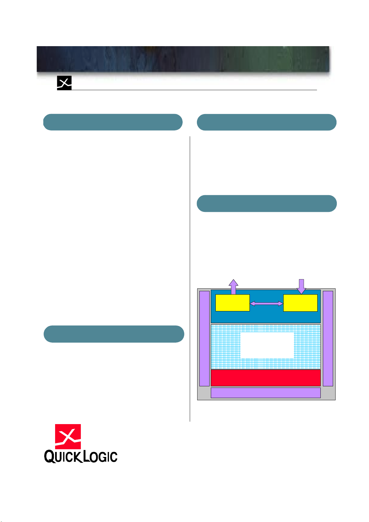
Fibre Channel Block Diagram
D
UAL PORT
SRAM
H
IGH SPEED CUSTOMIZABLE LOGIC
RAM Blocks
22 Blocks (25K bits)
IO Pins
Fibre Channel ENDEC
Customizable
Logic Cells
IO Pins
Transmit
Receive
10 bit/20 bit 10 bit/20 bit
IO Pins
Page 2
2Preliminary
2
QL80FC - QuickFC
TM
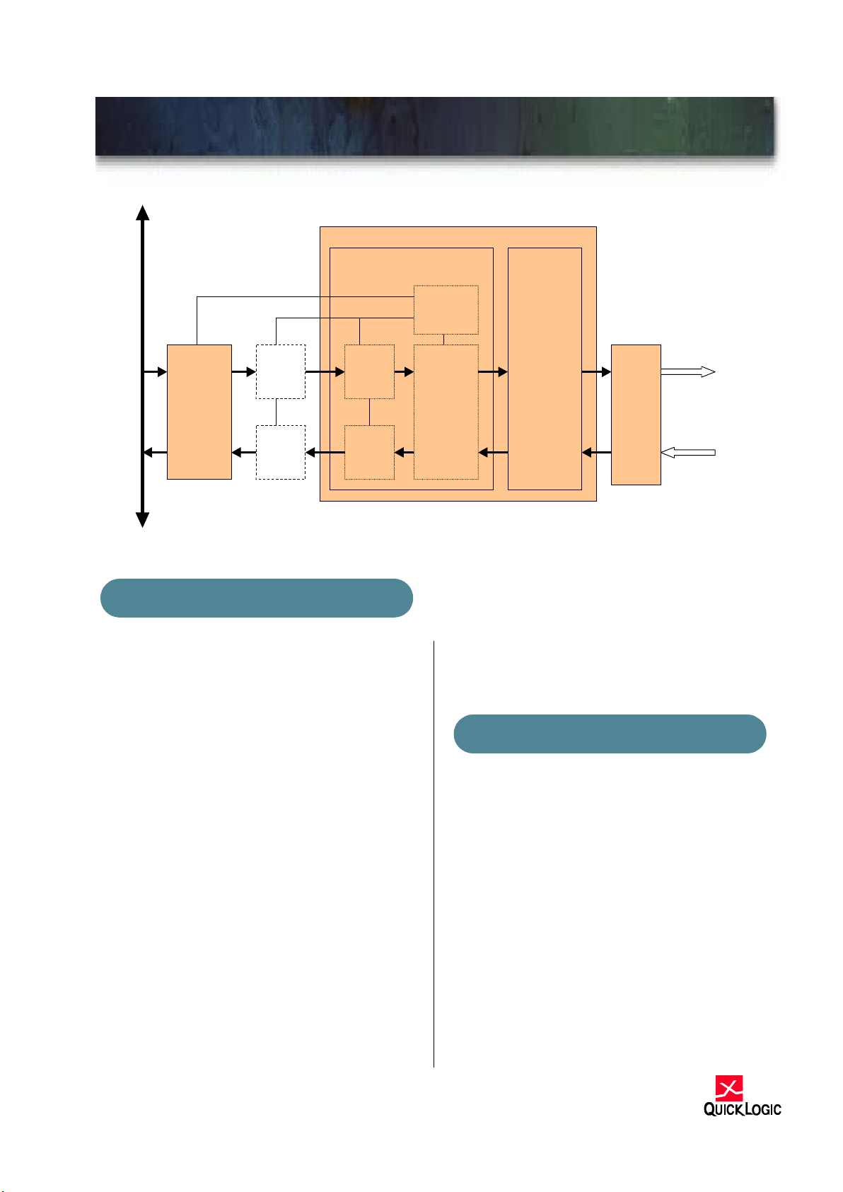
FIGURE 1. System Level Diagram
General Description
The QL80FC device in the QuickLogic QuickFC ESP
(Embedded Standard Product) family provides a completely integrated configurable Fibre Channel
Encoder/Decoder interface solution combined with
customizable logic. This device provides a means to
receive and transmit high-speed serial data and
implement a Fibre Channel Link interface or any
proprietary high-speed serial link.
The chip is divided into two main portions, an
embedded design and a customizable design. The
embedded design contains the built in functionality of
Fibre Channel's FC-1 and FC-2 layers, which the system designer uses as a standard product. This portion
can not be modified. As such, all functionality and
timing requirements have been verified in hardware
and are guaranteed.
The customizable portion consists of user customizable system gates, and interfaces directly to the
embedded portion of the chip. These gates may be
programmed to implement glue logic to other bus
standards such as PCI or SCSI. They can also be programmed with Fibre Channel Upper Layer Protocols.
Of course, the designer may choose to modify Upper
Layer Protocols for customization. In this way, the
QuickLogic QL80FC provides the embedded systems
designer with an easy to use and cost effective solution for embedded serial applications.
Fibre Channel Application
The QL80FC ENDEC is a high performance
encoder/decoder designed for use in conjunction
with Gb/s SERDES transmitter/receiver chips. These
chips, when combined with internal FIFO buffer
memory, can be used to build a complete serial link.
Optional, external FIFOs can be used in place of the
available internal FIFOs to extend buffering to sizes
beyond 352 words.
The embedded ENDEC is a full duplex design with an
encoder section for transmission and a decoder section for reception. The transmitter/encoder section
accepts a 4-byte user data word, encodes each byte
into a 10-bit transmission character and outputs
transmission characters to the SERDES transmitter.
This equals two 10-bit characters per clock (one 10bit character per clock in 10-bit mode). The receiver/
decoder section accepts two 10-bit transmission char-
System
Bus
(Optional)
Transmit
FIFO
(Optional)
Recei ve
FIFO
FIFO Control
User Customizabl e
Logic
Embedded
Fibre Channel
ENDEC
QL80FC Programmable ENDEC Chip
Bridge Logic
For Dat a Path
Transmit/
Recei ve
SERDES
2.5 Gb/s Serial
Data Ove r
Copper or
Optical Cable
Internal
Transmit
FIFO
Internal
Receive
FIFO
Micro- Process or
Or
System Bus
Interface
G
ENERAL DESCRIPTION
F
IBRE CHANNEL APPLICATIONS
Page 3
3
QL80FC - QuickFC
TM
acters from the SERDES receiver (one 10-bit character in 10-bit mode), decodes them, and outputs a 4byte user data word.
The QL80FC has a system interface that emulates a
synchronous FIFO for ease of use. FIFOs allow maximum sustained performance of 400 MB/s running a
full duplex link. Their function is to handle the asynchronous interface between the bus data rate and the
different serial data rates, and handle phase and frequency differences inherent in serial links. Internal
FIFOs of 352 x 36 or external FIFOs can be used to
expand the buffering to accommodate multiple
frames.
The QL80FC includes the hardware necessary for
packetized data protection. Framing functions are
provided via Fibre Channel compliant command
words (ordered sets) for Start of Frame and End of
Frame. CRC generation and data frame verification
protect the Fibre Channel frame header and data
field when these framing functions are used.
The device provides a microprocessor interface that
allows the user to manage the serial link. Signals are
also provided to decode serial link error conditions
and differentiate between data and commands. The
QL80FC implements link synchronization with the
SERDES chip through the Loss of Synchronization
State Machine (LOS) as required by the ANSI FC-PH
specification. The LOS manages receiver word synchronization with the RxComDet (comma detect) signal.
The QL80FC is a versatile part that allows the system
designer to create proprietary or Fibre Channel compliant serial links by taking advantage of some, or all,
of the Fiber Channel compliant features. It has a
number of useful features for system designers of
proprietary links. One such feature is the ability to
send intraframe IDLEs. These characters are automatically sent if the FIFO is empty, but they do not
affect the CRC. In this mode the QL80FC allows
simple interfacing to systems where the flow of data
may be interrupted.
Embedded Design Functional Description
The embedded FC-1 and FC-2 layers are divided into
two functional groupings: the Transmit data path and
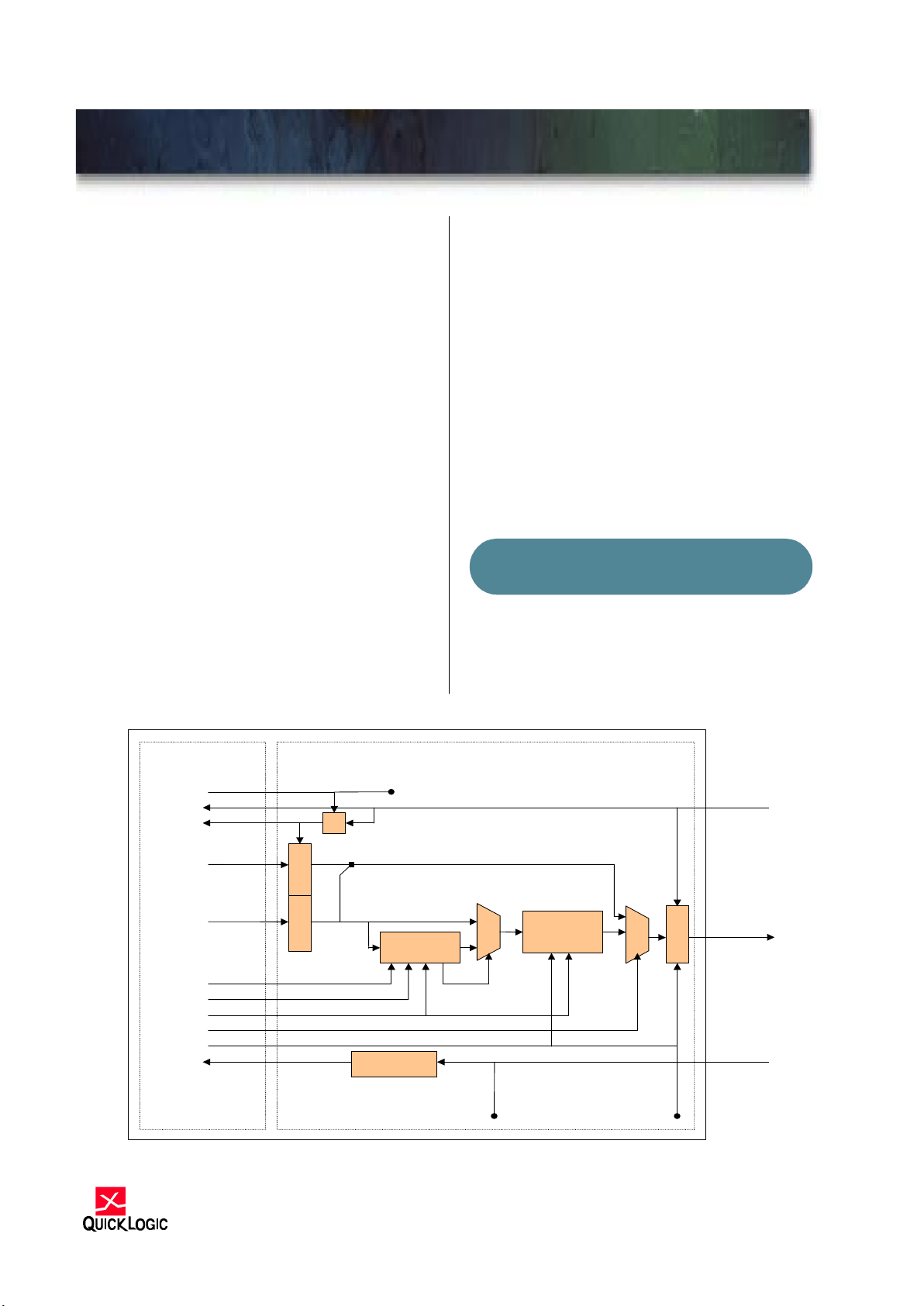
the Receive data path. A functional diagram for the
Transmit path is included in Figure 2.
FIGURE 2. Customizable ENDEC Chip Functional Block Diagram - Transmit and LCSM Data Paths
E
MBEDDED DESIGN
F
UNCTIONAL DESCRIPTION
CRC Generation
8b/10b Encoder
User Program mable
Logic
TxData[31:0]
Embedded Fibre Channel ENDEC
Registers
TxCrcEn
Registers
TxRawEn
TxOut[19:0]
TxClk125_inTxClk125_out
TxClk63
/2
TxRst
To receive data path
TxKChar
Async_rst
TenbMode
Registers
TxRData[39:32]
Async_rst
TenbMode
TxIF IdleEn
(only [9:0] used
in 10b mode)
TxClk63 Sync
Reset Circuit
Clk_rst
Clk_rst
To receive data path
Page 4

4Preliminary
4
QL80FC - QuickFC
TM
Transmit Data Path
When the transmit data path is in standard operation
(TxRawEn not asserted) the chip will latch an unencoded, Fibre Channel, 32-bit word on inputs
TxData[31:0]. This data then passes on to the 8b/
10b encoder, which creates a 40-bit encoded Fibre
Channel word. The encoder will encode the most significant character as a command character if the
TxKChar input line is asserted. This word is registered and passed to the SERDES in 20-bit chunks (10
bit chunks if 10 bit mode is enabled) on the TxOut
signal lines.
Asserting the TxCrcEn signal enables the CRC Generation block. This block will automatically detect the
SOF ordered set and begin CRC generation using the
ANSI specified CRC polynomial. It will continue until
an EOF or any other FC ordered set is encountered
(unless TxIFIdleEn is asserted, then the IDLE ordered
set will be ignored by the CRC generator). It then
inserts the CRC value into the data path for transmission to the SERDES.
The TxRawEn signal enables the raw transmit data
path when asserted. In this mode, the 8 bits of TxRData is concatenated onto the 32 bits of the TxData
signal to create a 40-bit wide data path. The CRC
generation and 8b/10b encoder blocks are bypassed
and the “raw” data latched at the inputs is passed
directly to the output registers that drive the SERDES. This mode is useful for testing the error handling capabilities of the serial link by providing the
systems designer a way to intentionally introduce
errors into the serial bit stream.
The TxIFIdleEn (Intra-Frame Idle Enable) input
enables the use of Fibre Channel IDLE words within
a Frame. When this signal is asserted, IDLE words
present within a data frame will not affect the value
generated by the CRC block. This feature is useful in
custom FC designs where it is desired to suspend the
transmission of a frame for a period of time and then
resume later.
The use of external FIFOs is optional. There is
enough RAM on the ENDEC chip to be configured
into two 352 x 36 FIFOs. If FIFOs of this size are all
that is required, external FIFOs would not be needed.
Synchronous read and writes directly from the system
bus without a FIFO is also possible.
Two clock signals are supplied to the customizable
logic on high speed, low skew clock networks:
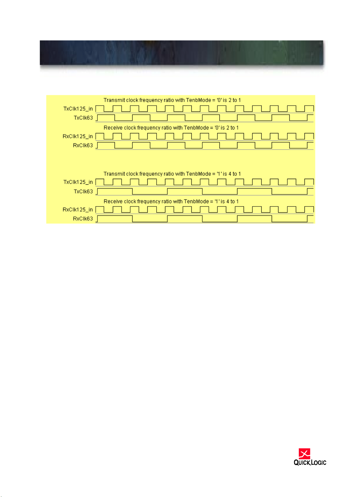
TxClk125 and TxClk63. TxClk125 is a clock running at a maximum speed of 125 MHz, and represents the “full speed” of the Oscillator being used to
clock the transmit data path. The input that drives
this signal is also used to clock the SERDES chip.
The TxClk63 clock signal operates at half the speed
of the TxClk125 clock. You will most likely want to
use the TxClk63 signal to clock your FIFOs and customizable logic. Of course, these signals can be
routed off-chip through the customizable I/O.
The Async_rst pin accepts an asynchronous, active
high reset signal. Circuitry takes this signal and synchronizes it with the TxClk63 clock. This synchronous reset signal, TxRst, is used to set or clear flipflops in the transmit data path. It is made available to
the user programmable logic for the same purpose
on a high speed, low skew network
The Clk_rst input stops the TxClk63 clock when this
signal is asserted. This signal was added primarily to
facilitate simulation. Clk_rst may be permanently
grounded in hardware.
T
RANSMIT DATA PATH
Page 5
5
QL80FC - QuickFC
TM
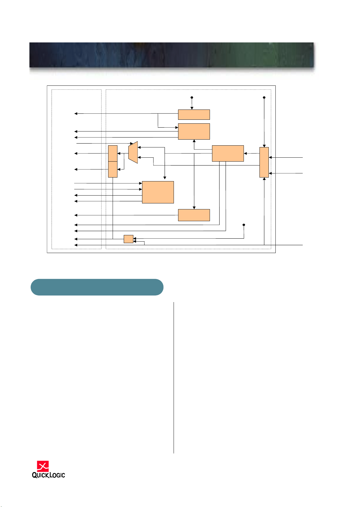
FIGURE 3. .Customizable ENDEC Chip Functional Block Diagram - Receive Data Path
Receive Data Path
Receive Data Path
The receive data path receives encoded data from an
on-board SERDES, decodes it and passes the resulting data to the customizable section of the chip. A
functional block diagram of the receive data path is
shown in Figure 3.
The RxClk125 signal latches 20 bits (10 bits when
10-bit mode is enabled) of data from the SERDES
into the RxIn input registers on the positive edge of
the clock. The RxClk125 signal is made available to
the customizable section. RxClk125 is divided by two
and made available to the customizable section on
the RxClk63 signal line. Both clocks use a high
speed, low skew clock network. Again you will most
likely want to use the RxClk63 signal to clock all registers and FIFOs in the receive data path. Registers
using RxClk125 and RxClk63 should be sensitive to
the rising edge of these clocks.
Once the data on the RxIn signal lines is latched into
the input registers, the data is passed on to the 8b/
10b decoder. Under standard operation, (input RxRa-
wEn is low), the data is decoded into 4, 8-bit characters and the resulting Fibre Channel word is placed
on the RxData[31:0] output signals. RxRData is not
used under normal operation. If the decoder detects a
Fibre Channel comma character in the most significant character of the word, the RxKChar signal line
will be asserted.
When the RxCrcEn signal is asserted the CRC checking logic will function. The CRC logic will automatically detect a SOF word and begin performing CRC
division on the next word in the data stream using the
ANSI specified CRC polynomial for Fibre Channel.
When an EOF word or any other FC ordered set is
detected (unless RxIFIdleEn is asserted, then the IDLE
ordered set will be ignored by the CRC checker) the
CRC will assert the RxCrcRdy signal for one cycle of
the RxClk63 clock. If the remainder for the division is
zero, the RxCrcOK signal line will also be asserted
during this same cycle.
User Programmable
Logic
Embedded Fibre Channel ENDEC
RxClk125_inRxClk125_ out
RxClk63
/2
8b/10b Decoder
Loss Of Sync
State Machine
CRC Checking
Ordered Set
Recogn ition
Registers
RxIn[19:0]
RxComDet
RxLOSync
RxLOSIdx[3:0]
RxData[31:0]
Registers
RxRawEn
RxKChar
RxCrcOK
RxCrcRdy
(SOF, ID LE, EOF . . . )RxSgpBus[14:0]
From transmit data path
Async_rst
RxCrcEn
(only [9:0] used
in 10b mode)
Registers
RxRData[39:32]
TenbMode
RxInvWord
RxIF IdleEn
RxClk63 Sync
Reset Circuit
RxRst
Clk_rst
From transmit
data path
R
ECEIVE DATA PATH
Page 6

6Preliminary
6
QL80FC - QuickFC
TM
When the RxRawEn signal is asserted the “raw” data
path will be enabled for the receive circuit. With the
“raw” data path enabled, the data received from the
SERDES does not pass through the 8b/10b decoder
or the CRC checking blocks. Instead it is routed
directly to the output registers and is made available
to the customizable section of the chip on signal lines
RxRData and RxData. This mode is useful for testing
the serial link.
The Loss of Synchronization State machine is
responsible for achieving character synchronization
on the data being sent from the SERDES. When the
Rst signal is asserted, the LOSSM goes to the “loss of
synchronization” state. In this state the RxLOSync
signal will be asserted. After the reception of three
valid command characters, the state machine will
proceed to the “synchronization acquired” state and
the RxLOSync signal is de-asserted. After the reception of 4 successive invalid characters the state
machine will return to the “Loss of Synchronization”
state. The value on the RxLOSIdx bus indicates the
state of LOSSM.
The ordered set recognition block detects Fibre
Channel ordered sets and asserts one signal line in
the RxSgpBus bus corresponding to the ordered set
detected. All 15 Fibre Channel ordered set types are
detected including SOF, EOF and IDLE. There is a list
of ordered sets detected by the ordered set recognition circuitry in Table 1.
There are two signals used to indicate that a word
having a decoding error of some kind is present on
the RxData outputs. When RxInvChar is asserted a
word with an invalid 10-bit representation is present
on the RxData signal lines. RxRDErr indicates an
invalid running disparity was detected on the currently available RxData word.
The Async_rst pin accepts an asynchronous, active
high reset signal. Circuitry takes this signal and synchronizes it with the RxClk63 clock. This synchronous reset signal, RxRst, is used to set or clear flipflops in the receive data path. It is made available to
the user programmable logic for the same purpose
on a high speed, low skew network.
The Clk_rst input stops the RxClk63 clock when this
signal is asserted. This signal was added primarily to
facilitate simulation. Clk_rst may be permanently
grounded in hardware.
Page 7

7
QL80FC - QuickFC
TM
Table of Recognized Ordered Sets
TABLE 1. Table of Recognized Ordered Sets
* Only recognized when RxIFIdleEn is asserted
R
ECOGNIZED ORDERED SETS
Beginning
RD
Identifier Ordered Set Code Hex
Equivalent
RxSgpBus Signal
Line Asserted
- SOFc1 K28.5 D21.5 D23.0 D23.0 BC B5 17 17 [0]
- SOFi1 K28.5 D21.5 D23.2 D23.2 BC B5 57 57 [0]
- SOFn1 K28.5 D21.5 D23.1 D23.1 BC B5 37 37 [0]
- SOFi2 K28.5 D21.5 D21.2 D21.1 BC B5 55 55 [0]
- SOFn2 K28.5 D21.5 D21.1 D21.1 BC B5 35 35 [0]
- SOFi3 K28.5 D21.5 D22.2 D22.2 BC B5 56 56 [0]
- SOFn3 K28.5 D21.5 D22.1 D22.1 BC B5 36 36 [0]
- SOFf K28.5 D21.5 D24.2 D24.2 BC B5 58 58 [0]
- EOFt K28.5 D21.4 D21.3 D21.3 BC 95 75 75 [1]
+ EOFt K28.5 D21.5 D21.3 D21.3 BC B5 75 75 [1]
- EOFdt K28.5 D21.4 D21.4 D21.4 BC 95 95 95 [1]
+ EOFdt K28.5 D21.5 D21.4 D21.4 BC B5 95 95 [1]
- EOFa K28.5 D21.4 D21.7 D21.7 BC 95 F5 F5 [1]
+ EOFa K28.5 D21.5 D21.7 D21.7 BC B5 F5 F5 [1]
- EOFn K28.5 D21.4 D21.6 D21.6 BC 95 D5 D5 [1]
+ EOFn K28.5 D21.5 D21.6 D21.6 BC B5 D5 D5 [1]
- EOFdti K28.5 D10.4 D21.4 D21.4 BC 8A 95 95 [1]
+ EOFdti K28.5 D10.5 D21.4 D21.4 BC AA 95 95 [1]
- EOFni K28.5 D10.4 D21.6 D21.6 BC 8A D5 D5 [1]
+ EOFni K28.5 D10.5 D21.6 D21.6 BC AA D5 D5 [1]
- IDLE K28.5 D21.4 D21.5 D21.5 BC 95 B5 B5 [2]
+ IDLE* K28.5 D21.5 D21.5 D21.5 BC B5 B5 B5 [2]
- R_RDY K28.5 D21.4 D10.2 D10.2 BC 95 4A 4A [3]
- OLS K28.5 K21.1 D10.4 D21.2 BC 35 8A 55 [4]
- NOS K28.5 D21.2 D31.5 D5.2 BC 55 BF 45 [5]
- LR K28.5 D9.2 D31.5 D9.2 BC 49 BF 49 [6]
- LRR K28.5 D21.1 D31.5 D9.2 BC 35 BF 49 [7]
- ARBx K28.5 D20.4 AL_PA AL_PA BC 4A xx xx [8]
- ARB(F0) K28.4 D20.4 D16.7 D16.7 BC 4A F0 F0 [8]
- OPNyx K28.5 D17.4 AL_PD AL_PS BC 91 yy xx [9]
- OPNyy K28.5 D17.4 AL_PD AL_PD BC 91 yy yy [9]
- OPNfr K28.5 D17.4 D31.7 D31.7 BC 91 FF FF [9]
- OPNyr K28.5 D17.4 AL_PD D31.7 BC 91 yy FF [9]
- CLS K28.5 D5.4 D21.5 D21.5 BC 85 B5 B5 [10]
- MRKtx K28.5 D31.2 MK_TP AL_PS BC 5F tt xx [11]
- LIP(F7,F7) K28.5 D21.0 D23.7 D23.7 BC 15 F7 F7 [12]
- LIP(F8,F7) K28.5 D21.0 D24.7 D23.7 BC 15 F8 F7 [12]
- LIP(F7,x) K28.5 D21.0 D23.7 AL_PS BC 15 F7 xx [12]
- LIP(F8,x) K28.5 D21.0 D24.7 AL_PS BC 15 F8 xx [12]
- LIP(y,x) K28.5 D21.0 AL_PD AL_PS BC 15 yy xx [12]
- LPEyx K28.5 D5.0 AL_PD AL_PS BC 05 yy xx [13]
- LPEfx K28.5 D5.0 D31.7 AL_PS BC 05 FF xx [13]
- LPByx K28.5 D9.0 AL_PD AL_PS BC 09 yy xx [14]
Page 8

8Preliminary
8
QL80FC - QuickFC
TM
Dedicated I/O Pins
Customizable Interface Signals
S
IGNAL DEFINITIONS
Async_rst input active high, asynchronous reset
TxOut[19:0] output data transmitted to SERDES (only lines [9:0] are used in 10 bit mode)
TxClk125_in input transmit clock up to 125 MHz
RxIn[19:0] input data received from SERDES
RxClk125_in input receive clock up to 125 MHz
RxComDet input Fibre Channel comma character detected
ResIn[2:0] input reserved for QuickLogic use, hold low or high
TenbMode input enables 10 bit interface to SERDES when asserted
Clk_rst Input Stops TxClk63 and RxClk63 when high. Tie Low.
TxRst output active high reset signal for transmit path, synchronous with TxClk63
TxData[31:0] input 32 bit Fibre Channel word to be encoded for transmit path
TxRData[39:32] input only used when TxRawEn is asserted. Combines with TxData to
construct 40 bit raw data for transmit path
TxCrcEn input enables CRC error value generation when asserted
TxIFIdleEn Input enables Intra-Frame IDLE support for transmit path when asserted
TxRawEn input select between raw and encoded data modes for transmit data path
TxKChar input indicates that the most significant byte of data word is a K character
TxClk125 output full speed transmit clock up to 125 MHz (use the rising edge)
TxClk63 output half speed transmit clock up to 63 MHz (use the rising edge)
RxData[31:0] output 32 bit Fibre Channel word decoded by the ENDEC receive path.
RxRData[39:32] output only used when RxRawEn is asserted. Combines with RxData to
construct 40 bit raw data through the ENDEC receive path
RxRawEn input select between raw and encoded data modes for receive data path
RxKChar output asserted when most significant byte of data word is a K character
RxSgpBus[14:0] output bus indicating when an ordered set is detected. One signal line is asserted
corresponding to the type of ordered set detected:
[0] – SOF [5] – NOS [10] – CLS
[1] – EOF [6] – LR [11] – MRK
[2] – IDLE [7] – LRR [12] – LIP
[3] – R_RDY [8] – ARB [13] – LPE
[4] – OLS [9] – OPN [14] – LPB
RxCrcRdy output asserted when available data is a CRC word
RxCrcOK output asserted when CRC remainder is zero
RxCrcEn input enables CRC error checking for the receive data path when asserted
RxIFIdleEn input enables Intra-Frame IDLE support for receive path when asserted
RxLOSync output asserted when bit synchronization with the SERDES has been lost
RxLOSIdx[3:0] output index indicating state of Loss of Sync state machine
RxInvChar output asserted when available data has an invalid encoding error
RxClk125 output full speed receive clock up to 125 MHz (use the rising edge)
RxClk63 output half speed receive clock up to 63 MHz (use the rising edge)
RxRst output active high reset signal for receive data path, synchronous with RxClk63
ResOut[2:0] output reserved for QuickLogic use, do not connect to these outputs
Page 9

9
QL80FC - QuickFC
TM
A wide range of additional features complements the
QL80FC device. The FPGA portion of the device is
5-volt and 3.3-volt compliant and can perform highspeed logic functions such as 160 MHz FIFOs. I/O
pins provide individually controlled output enables,
dedicated input/feedback registers, and full JTAG
capability for boundary scan and test. In addition, the
QL80FC device provides the benefits of non-volatility, high design security, immediate functionality on
power-up, and a single chip solution.
The QL80FC customizable logic architecture consists
of an array of user-configurable logic building blocks,
called logic cells, set beneath a grid of metal wiring
channels similar to those of a gate array. Through
ViaLink
®
elements located at the wire intersections,
the output(s) of any cell may be programmed to connect to the input(s) of any other cell. Using the customizable logic in the QL80FC, designers can quickly
and easily customize their “back-end” design for any
number of applications.
FIGURE 4. Logic Cell
Array of Logic Cells
The QL80FC device has 22 1,152-bit RAM modules, for a total of 25,344 RAM bits. Using two
“mode” pins, designers can configure each module
into 64 (deep) x18 (wide), 128x9, 256x4, or 512x2
blocks. See the table below. The blocks are also easily cascadable to increase their effective width or
depth.
RAM Module Features
The RAM modules are “dual-ported”, with completely independent READ and WRITE ports and
separate READ and WRITE clocks. The READ ports
support asynchronous and synchronous operation,
while the WRITE ports support synchronous operation. Each port has 18 data lines and 9 address lines,
allowing word lengths of up to 18 bits and address
spaces of up to 512 words. Depending on the mode
selected, however, some higher order data or address
lines may not be used.
A
RRAY OF LOGIC CELLS
QS
A1
A2
A3
A4
A5
A6
OS
OP
B1
B2
C1
C2
MS
D1
E1
NP
E2
D2
NS
F1
F3
F5
F6
F2
F4
QC
QR
MP
AZ
OZ
QZ
NZ
FZ
Mode: Address
Buses [a:0]
Data Buses
[w:0]
64x18 [5:0] [17:0]
128x9 [6:0] [8:0]
256x4 [7:0] [3:0]
512x2 [8:0] [1:0]
RAM M
ODULE FEATURES
Page 10
10Preliminary
10
QL80FC - QuickFC
TM
The Write Enable (WE) line acts as a clock enable for
synchronous write operation. The Read Enable (RE)
acts as a clock enable for synchronous READ operation (ASYNCRD input low), or as a flow-through
enable for asynchronous READ operation (ASYNCRD input high).
FIGURE 5. RAM Module
Designers can cascade multiple RAM modules to
increase the depth or width allowed in single modules
by connecting corresponding address lines together
and dividing the words between modules. This
approach allows up to 512-deep configurations as
large as 16 bits wide in the QL80FC device.
A similar technique can be used to create depths
greater than 512 words. In this case, address signals
higher than the eighth bit are encoded onto the write
enable (WE) input for WRITE operations. The READ
data outputs are multiplexed together using encoded
higher READ address bits for the multiplexer
SELECT signals.
JTAG Support
JTAG pins support IEEE standard 1149.1a to provide boundary scan capability for the QL80FC
device. Six pins are dedicated to JTAG and programming functions on each QL80FC device, and are
unavailable for general design input and output sig-
nals. TDI, TDO, TCK, TMS, and TRSTB are JTAG
pins. A sixth pin, STM, is used only for programming.
Software support for the QL80FC device is available
through the QuickWork s
TM
development package.
This turnkey PC-based QuickWo r ks package, shown
in Figure 6, provides a complete ESP software solution with design entry, logic synthesis, place and
route, and simulation. QuickWorks includes VHDL,
Verilog, schematic, and mixed-mode entry with fast
and efficient logic synthesis provided by the integrated Synplicity Synplify Lite
TM
tool, specially tuned
to take advantage of the QL80FC architecture.
QuickWork s also provides functional and timing simulation for guaranteed timing and source-level debugging.
The UNIX-based QuickToo l s
TM
package is a subset of
QuickWork s and provides a solution for designers
who use schematic-only design flow or third-party
tools for design entry, synthesis, or simulation.
FIGURE 6. QuickWorks Tool Suite
Development Tools
MODE[1:0]
WA[a:0]
WD[w:0]
WE
WCLK
RAM Module
ASYNCRD
RA[a:0]
RD[w:0]
RE
RCLK
JTAG S
UPPORT
D
EVELOPMENT TOOLS
Schematic
Schematic
Turbo
HDL Editor
Third Party
Design
Entry
& Synthesis
Third Party
Simulation
VHDL/
VHDL/
Verilog
Verilog
SCS
Tools
Silos III
Simulator
SpDE
Mixed-Mode Design
Synplify-
HDL
Synthesis
Quick
Works
Design Software
Aldec
Page 11

11
QL80FC - QuickFC
TM
QL80FC External Device Pins
*See QuickNote 65 on the QuickLogic web site for
information on RAM initialization.
QL80FC E
XTERNAL DEVICE PINS
Type Description
IN Input. A standard input-only
signal.
OUT Totem pole output. A standard
active output driver.
T/S Tri-state. A bi-directional, tri-state
input/output pin.
S/T/S Sustained Tri-state. An active low
tri-state signal driven by one PCI
agent at a time. It must be driven
high for at least one clock before
being disabled (set to Hi-Z). A pullup needs to be provided by the
PCI system central resource to
sustain the inactive state once the
active driver has released the signal.
O/D Open Drain. Allows multiple
devices to share this pin as a
wired-or.
Pin/Bus
Name
Type Function
VCC IN Supply pin. Tie to 3.3V supply.
VCCIO IN Supply pin for I/O. Set to 3.3V for
3.3V I/O, 5V for 5.0V compliant I/O.
GND IN Ground pin. Tie to GND on the PCB.
I/O T/S Programmable Input/Output/Tri-State/
Bi-directional Pin.
GLCK/I IN Programmable Global Network or
Input-only pin. Tie to VCC or GND if
unused.
ACLK/I IN Programmable Array Network or Input-
only pin. Tie to VCC or GND if unused.
TDI/
RSI*
IN JTAG Data In/Ram Init. Serial Data In.
Tie to VCC if unused. Connect to Serial
EPROM data for RAM init.
TDO/
RCO*
OUT JTAG Data Out/Ram Init Clock. Leave
unconnected if unused. Connect to
Serial EPROM clock for RAM init.
TCK IN JTAG Clock. Tie to GND if unused.
TMS IN JTAG Test Mode Select. Tie to VCC if
unused.
TRSTB/
RRO*
IN JTAG Reset/RAM Init. Reset Out. Tie
to GND if unused. Connect to Serial
EPROM reset for RAM init.
STM IN QuickLogic Reserved pin. Tie to GND
on the PCB.
Page 12
12Preliminary
12
QL80FC - QuickFC
TM
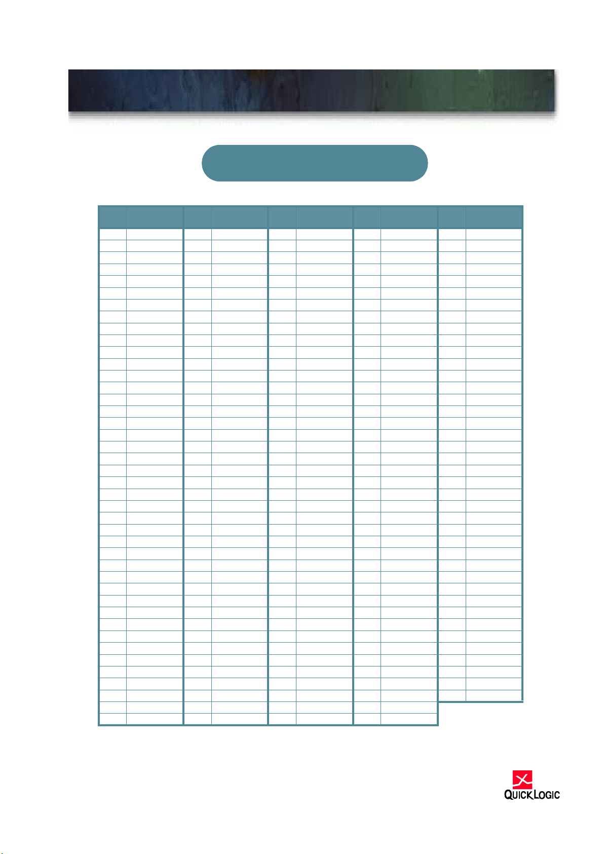
PQFP 208
P
INOUT TABLE
208
PQFP
Function 208
PQFP
Function 208
PQFP
Function 208
PQFP
Function 208
PQFP
Function
1 I/O 43 GND 85 TxOut[4] 127 GND 169 I/O
2 I/O 44 I/O 86 TxOut[5] 128 I/O 170 I/O
3 I/O 45 I/O 87 TxOut[6] 129 GLCK/I 171 I/O
4 I/O 46 I/O 88 TxOut[7] 130 ACLK/I 172 I/O
5 I/O 47 I/O 89 TxOut[8] 131 VCC 173 I/O
6 I/O 48 I/O 90 TxOut[9] 132 ResIn[1] 174 I/O
7 I/O 49 I/O 91 TxOut[10] 133 ResIn[2] 175 I/O
8 I/O 50 I/O 92 TxOut[11] 134 VCC 176 I/O
9 I/O 51 I/O 93 TxOut[12] 135 I/O 177 GND
10 VCC 52 I/O 94 TxOut[13] 136 I/O 178 I/O
11 I/O 53 I/O 95 GND 137 I/O 179 I/O
12 GND 54 TDI 96 TxOut[14] 138 I/O 180 I/O
13 I/O 55 RxComDet 97 VCC 139 I/O 181 I/O
14 I/O 56 RxIn[0] 98 TxOut[15] 140 I/O 182 GND
15 I/O 57 RxIn[1] 99 TxOut[16] 141 I/O 183 I/O
16 I/O 58 RxIn[2] 100 TxOut[17] 142 I/O 184 I/O
17 I/O 59 GND 101 TxOut[18] 143 I/O 185 I/O
18 I/O 60 RxIn[3] 102 TxOut[19] 144 I/O 186 I/O
19 I/O 61 VCC 103 TRSTB 145 VCC 187 VCCIO
20 I/O 62 RxIn[4] 104 TMS 146 I/O 188 I/O
21 I/O 63 RxIn[5] 105 I/O 147 GND 189 I/O
22 I/O 64 RxIn[6] 106 I/O 148 I/O 190 I/O
23 GND 65 RxIn[7] 107 I/O 149 I/O 191 I/O
24 I/O 66 RxIn[8] 108 I/O 150 I/O 192 I/O
25 ResIn[0] 67 RxIn[9] 109 I/O 151 I/O 193 I/O
26 TxClk125_in 68 RxIn[10] 110 I/O 152 I/O 194 I/O
27 VCC 69 RxIn[11] 111 I/O 153 I/O 195 I/O
28 Rst 70 RxIn[12] 112 I/O 154 I/O 196 I/O
29 RxClk125_in 71 RxIn[13] 113 I/O 155 I/O 197 I/O
30 VCC 72 RxIn[14] 114 VCC 156 I/O 198 I/O
31 I/O 73 GND 115 I/O 157 TCK 199 GND
32 I/O 74 RxIn[15] 116 GND 158 STM 200 I/O
33 I/O 75 RxIn[16] 117 I/O 159 I/O 201 VCC
34 I/O 76 RxIn[17] 118 I/O 160 I/O 202 I/O
35 I/O 77 RxIn[18] 119 I/O 161 I/O 203 I/O
36 I/O 78 GND 120 I/O 162 I/O 204 I/O
37 I/O 79 RxIn[19] 121 I/O 163 GND 205 I/O
38 I/O 80 TxOut[0] 122 I/O 164 I/O 206 I/O
39 I/O 81 TxOut[1] 123 I/O 165 VCC 207 TDO
40 I/O 82 TxOut[2] 124 I/O 166 I/O 208 I/O
41 VCC 83 VCCIO 125 I/O 167 I/O
42 I/O 84 TxOut[3] 126 I/O 168 I/O
Page 13
13
QL80FC - QuickFC
TM
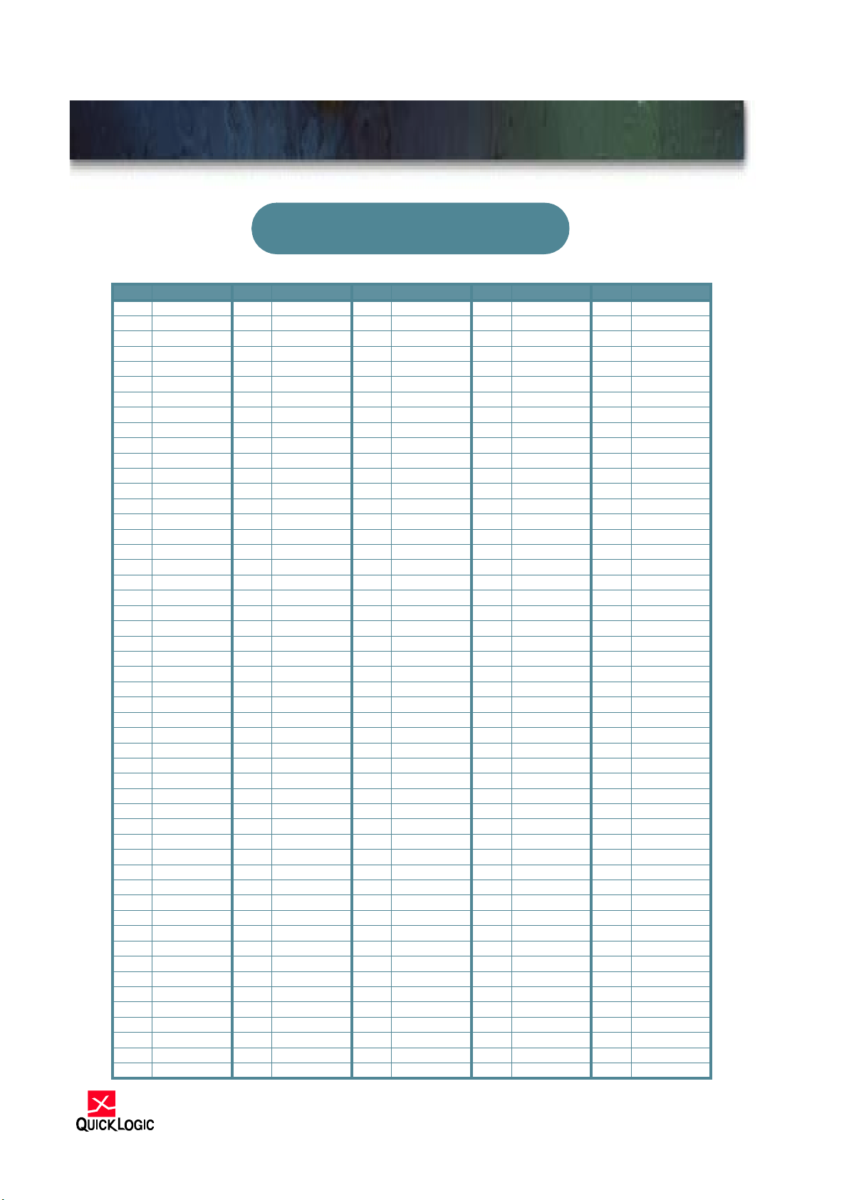
PQFP 456 Pinout Table
PBGA 456
P
INOUT TABLE
456 Function 456 Function 456 Function 456 Function 456 Function
A1 I/O B26 STM D25 I/O H4 I/O M14 GND/THERM
A2 I/O C1 I/O D26 I/O H5 NC M15 GND/THERM
A3 I/O C2 I/O E1 I/O H22 NC M16 GND/THERM
A4 I/O C3 I/O E2 I/O H23 I/O M22 NC
A5 I/O C4 TDO E3 I/O H24 I/O M23 NC
A6 I/O C5 I/O E4 I/O H25 I/O M24 I/O
A7 I/O C6 I/O E5 GND H26 I/O M25 I/O
A8 I/O C7 I/O E6 VCC J1 I/O M26 I/O
A9 I/O C8 I/O E7 GND J2 I/O N1 Async_rst
A10 I/O C9 I/O E8 NC J3 I/O N2 I/O
A11 I/O C10 I/O E9 GND J4 NC N3 I/O
A12 VCCIO C11 I/O E10 I/O J5 GND N4 ResIn[0]
A13 I/O C12 I/O E11 GND J22 NC N5 VCC
A14 I/O C13 I/O E12 GND J23 NC N11 GND/THERM
A15 I/O C14 I/O E13 VCC J24 I/O N12 GND/THERM
A16 I/O C15 I/O E14 GND J25 I/O N13 GND/THERM
A17 I/O C16 I/O E15 GND J26 I/O N14 GND/THERM
A18 I/O C17 I/O E16 GND K1 I/O N15 GND/THERM
A19 I/O C18 I/O E17 NC K2 I/O N16 GND/THERM
A20 I/O C19 I/O E18 GND K3 I/O N22 GND
A21 I/O C20 I/O E19 NC K4 I/O N23 I/O
A22 I/O C21 I/O E20 GND K5 VCC N24 I/O
A23 I/O C22 I/O E21 VCC K22 GND N25 I/O
A24 I/O C23 I/O E22 GND K23 I/O N26 I/O
A25 I/O C24 I/O E23 I/O K24 I/O P1 I/O
A26 I/O C25 TCK E24 I/O K25 I/O P2 I/O
B1 I/O C26 I/O E25 I/O K26 I/O P3 I/O
B2 I/O D1 I/O E26 I/O L1 I/O P4 I/O
B3 I/O D2 I/O F1 I/O L2 I/O P5 NC
B4 I/O D3 I/O F2 I/O L3 I/O P11 GND/THERM
B5 I/O D4 GND F3 I/O L4 I/O P12 GND/THERM
B6 I/O D5 I/O F4 NC L5 NC P13 GND/THERM
B7 I/O D6 NC F5 VCC L11 GND/THERM P14 GND/THERM
B8 I/O D7 I/O F22 VCC L12 GND/THERM P15 GND/THERM
B9 I/O D8 I/O F23 NC L13 GND/THERM P16 GND/THERM
B10 I/O D9 GND F24 I/O L14 GND/THERM P22 NC
B11 I/O D10 I/O F25 I/O L15 GND/THERM P23 ResIn[1]
B12 I/O D11 I/O F26 I/O L16 GND/THERM P24 ResIn[2]
B13 I/O D12 GND G1 I/O L22 NC P25 I/O
B14 I/O D13 I/O G2 I/O L23 I/O P26 ACLK / I
B15 I/O D14 I/O G3 I/O L24 I/O R1 I/O
B16 I/O D15 GND G4 I/O L25 I/O R2 I/O
B17 I/O D16 I/O G5 NC L26 I/O R3 I/O
B18 I/O D17 I/O G22 GND M1 TxClk125_in R4 NC
B19 I/O D18 GND G23 I/O M2 RxClk125_in R5 NC
B20 I/O D19 I/O G24 I/O M3 I/O R11 GND/THERM
B21 I/O D20 I/O G25 I/O M4 NC R12 GND/THERM
B22 I/O D21 NC G26 I/O M5 GND R13 GND/THERM
B23 I/O D22 I/O H1 I/O M11 GND/THERM R14 GND/THERM
B24 I/O D23 GND H2 I/O M12 GND/THERM R15 GND/THERM
B25 I/O D24 I/O H3 I/O M13 GND/THERM R16 GND/THERM
Page 14

14Preliminary
14
QL80FC - QuickFC
TM
456 Function 456 Function 456 Function 456 Function
R22 VCC Y1 I/O AC6 NC AE5 RxIn[3]
R23 NC Y2 I/O AC7 I/O AE6 RxIn[4]
R24 I/O Y3 I/O AC8 I/O AE7 RxIn[5]
R25 I/O Y4 I/O AC9 NC AE8 RxIn[6]
R26 GCLK / I Y5 I/O AC10 I/O AE9 RxIn[7]
T1 I/O Y22 GND AC11 I/O AE10 RxIn[8]
T2 I/O Y23 I/O AC12 NC AE11 RxIn[9]
T3 I/O Y24 I/O AC13 I/O AE12 I/O
T4 I/O Y25 I/O AC14 VCCIO AE13 TxOut[0]
T5 VCC Y26 I/O AC15 NC AE14 TxOut[2]
T11 GND/THERMAL AA1 I/O AC16 I/O AE15 TxOut[4]
T12 GND/THERMAL AA2 I/O AC17 I/O AE16 TxOut[6]
T13 GND/THERMAL AA3 NC AC18 NC AE17 TxOut[8]
T14 GND/THERMAL AA4 NC AC19 I/O AE18 TxOut[10]
T15 GND/THERMAL AA5 VCC AC20 I/O AE19 TxOut[12]
T16 GND/THERMAL AA22 VCC AC21 I/O AE20 TxOut[14]
T22 GND AA23 NC AC22 NC AE21 TxOut[16]
T23 I/O AA24 I/O AC23 GND AE22 TxOut[18]
T24 I/O AA25 I/O AC24 I/O AE23 NC
T25 I/O AA26 I/O AC25 I/O AE24 TMS
T26 I/O AB1 I/O AC26 I/O AE25 I/O
U1 I/O AB2 I/O AD1 I/O AE26 I/O
U2 I/O AB3 I/O AD2 NC AF1 I/O
U3 I/O AB4 I/O AD3 I/O AF2 I/O
U4 I/O AB5 GND AD4 I/O AF3 RxIn[10]
U5 GND AB6 VCC AD5 I/O AF4 RxIn[11]
U22 NC AB7 NC AD6 I/O AF5 RxIn[12]
U23 I/O AB8 NC AD7 I/O AF6 RxIn[13]
U24 I/O AB9 NC AD8 I/O AF7 RxIn[14]
U25 I/O AB10 VCC AD9 I/O AF8 RxIn[15]
U26 I/O AB11 GND AD10 I/O AF9 RxIn[16]
V1 I/O AB12 NC AD11 I/O AF10 RxIn[17]
V2 I/O AB13 I/O AD12 RxComDet AF11 RxIn[18]
V3 I/O AB14 GND AD13 I/O AF12 RxIn[19]
V4 NC AB15 VCC AD14 I/O AF13 TxOut[1]
V5 NC AB16 I/O AD15 I/O AF14 TxOut[3]
V22 GND AB17 NC AD16 I/O AF15 TxOut[5]
V23 NC AB18 VCC AD17 I/O AF16 TxOut[7]
V24 I/O AB19 GND AD18 I/O AF17 TxOut[9]
V25 I/O AB20 NC AD19 I/O AF18 TxOut[11]
V26 I/O AB21 VCC AD20 I/O AF19 TxOut[13]
W1 I/O AB22 GND AD21 I/O AF20 TxOut[15]
W2 I/O AB23 I/O AD22 I/O AF21 TxOut[17]
W3 I/O AB24 I/O AD23 TRSTB AF22 TxOut[19]
W4 I/O AB25 I/O AD24 I/O AF23 I/O
W5 NC AB26 I/O AD25 I/O AF24 I/O
W22 NC AC1 I/O AD26 I/O AF25 I/O
W23 I/O AC2 I/O AE1 TDI AF26 I/O
W24 I/O AC3 NC AE2 RxIn[0]
W25 I/O AC4 GND AE3 RxIn[1]
W26 I/O AC5 I/O AE4 RxIn[2]
Page 15

15
QL80FC - QuickFC
TM
Timing Diagrams
FIGURE 7. Transmit Timing Diagram
Transmit Timing Characteristics
FIGURE 8. Receive Timing Diagram
Receive Timing Characteristics
T
IMING
D
IAGRAMS
Parameter Description Min Typ Max Units
T1 Clock to Out 2.5 3.7 5.6 ns
Parameter Description Min Typ Max Units
T1 Setup time 0.0 ns
T2 Hold time 2.3 1.5 ns
Page 16
16Preliminary
16
QL80FC - QuickFC
TM
FIGURE 9. Clock Frequency Ratios are Dependent on tenbMode setting
Page 17

17
QL80FC - QuickFC
TM
Reference Development Kit
QuickLogic has designed an evaluation board, which
will allow the system designer to test their designs in
hardware. The board plugs into a PCI expansion slot
in a Windows PC and allows the user to communicate with the QuickLogic ENDEC chip via a user
modifiable software script and the PCI bus. The block
diagram for the board is shown below. PCI speeds of
up to 64 bits at 75 MHz are supported via QuickLogic's QL5064 device, enabling system read/write
speeds matching those of the Fibre Channel link.
There is a socket for the ENDEC chip, and connection points for a logic analyzer on the board. There is
also a GBIC Fibre Channel connector on the board
to allow communication with other Fibre Channel
devices.
A Reference Design is supplied by QuickLogic to
load into the programmable portion of the ENDEC
chip. The Reference Design code will allow the system designer to immediately have an operational
chip for use on the reference board. The source code
for the reference design and software is available to
the system designer for use or modification as he or
she wishes, free of charge.
FIGURE 10. Reference Board Block Diagram
R
EFERENCE DEVELOPMENT KIT
PCI
Bus
Transmit
FIFO
Receive
FIFO
FIFO Control
User Customizable
Logic
Embedded
Fibre Channel
ENDEC
QuickLogic QL80FC Programmable
ENDEC Chip
Glue Logic
for FIFO
Interface
Transmit/
Receive
SERDES
GBIC
Media
I/O
2.5 Gb/s
QuickLogic
QL5064
75MHz/64 bit
PCI Controller
125 MHz
Oscillator
LED Indicators
8 Bit Data
Bus
Page 18

18Preliminary
18
QL80FC - QuickFC
TM
Absolute Maximum Ratings
VCC Voltage . . . . . . . . . . . . . . . . -0.5 to 4.6V
VCCIO Voltage . . . . . . . . . . . . . . -0.5 to 7.0V
Input Voltage . . . . . . . . -0.5V to VCCIO +0.5V
Latch-up Immunity
. . . . . . . . . . . . ±200mA
DC Input Current
. . . . . . . . . . . . ±20 mA
ESD Pad Protection . . . . . . . . . . . ±2000V
Storage Temperature . . . . . . -65ºC to + 150ºC
Lead Temperature . . . . . . . . . . . . . . . . 300
ºC
Operating Range
DC Characteristics
Notes:
[1] Capacitance is sample tested only.
[2] Only one output at a time. Duration should not exceed 30 seconds.
[3] See Application Note 32: Power calculations for QuickLogic devices.
Symbol Parameter Industrial Commercial Unit
Min Max Min Max
VCC Supply Voltage 3.0 3.6 3.0 3.6 V
VCCIO I/O Input Tolerance Voltage 3.0 5.5 3.0 5.25 V
TA Ambient Temperature -40 85 0 70
°
C
K Delay Factor -A Speed Grade 0.43 0.90 0.46 0.88
Symbol Parameter Conditions Min Max Unit
VIH Input HIGH Voltage 0.5VCC VCCIO+0.5 V
VIL Input LOW Voltage -0.5 0.3VCC V
VOH Output HIGH Voltage IOH = -12 mA 2.4 V
IOH = -500 µA
0.9VCC V
VOL Output LOW Voltage IOL = 16 mA 0.45 V
IOL = 1.5 mA 0.1VCC V
II I or I/O Input Leakage Current VI = VCCIO or GND -10 10
µ
A
IOZ 3-State Output Leakage Current VI = VCCIO or GND -10 10
µ
A
CI Input Capacitance [1] 10 pF
IOS Output Short Circuit Current [2] VO = GND -15 -180 mA
VO = VCC 40 210 mA
ICC D.C. Supply Current [3] VI, VIO = VCCIO or GND 0.50 (t
yp)
2mA
ICCIO D.C. Supply Current on VCCIO 0 100
µ
A
Page 19

19
QL80FC - QuickFC
TM
AC CHARACTERISTICS at VCC = 3.3V, TA = 25°C (K = 1.00)
(To calculate delays, multiply the appropriate K factor in the “Operating Range” section by the following numbers.)
Logic Cells
RAM Cell Synchronous Write Timing
Notes:
[4] Stated timing for worst case Propagation Delay over process variation at VCC=3.3V and TA=25°C. Multiply by
the appropriate Delay Factor, K, for speed grade, voltage and temperature settings as specified in the Operating
Range.
[5] These limits are derived from a representative selection of the slowest paths through the QuickRAM logic cell
including typical net delays. Worst case delay values for specific paths should be determined from timing analysis of your particular design.
Symbol Parameter
Propagation Delays (ns)
Fanout [5]
12348
tPD Combinatorial Delay [6] 1.4 1.7 1.9 2.2 3.2
tSU Setup Time [6] 1.7 1.7 1.7 1.7 1.7
tH Hold Time 0.0 0.0 0.0 0.0 0.0
tCLK Clock to Q Delay 0.7 1.0 1.2 1.5 2.5
tCWHI Clock High Time 1.2 1.2 1.2 1.2 1.2
tCWLO Clock Low Time 1.2 1.2 1.2 1.2 1.2
tSET Set Delay 1.0 1.3 1.5 1.8 2.8
tRESET Reset Delay 0.8 1.1 1.3 1.6 2.6
tSW Set Width 1.9 1.9 1.9 1.9 1.9
tRW Reset Width 1.8 1.8 1.8 1.8 1.8
Symbol Parameter
Propagation Delays (ns)
Fanout
[4]
12348
TSWA WA Setup Time to WCLK 1.0 1.0 1.0 1.0 1.0
THWA WA Hold Time to WCLK 0.0 0.0 0.0 0.0 0.0
TSWD WD Setup Time to WCLK 1.0 1.0 1.0 1.0 1.0
THWD WD Hold Time to WCLK 0.0 0.0 0.0 0.0 0.0
TSWE WE Setup Time to WCLK 1.0 1.0 1.0 1.0 1.0
THWE WE Hold Time to WCLK 0.0 0.0 0.0 0.0 0.0
TWCRD WCLK to RD (WA=RA) [4] 5.0 5.3 5.6 5.9 7.1
Page 20

20Preliminary
20
QL80FC - QuickFC
TM
RAM Cell Synchronous Read Timing
RAM Cell Asynchronous Read Timing
Input-Only Cells
Clock Cells
Notes:
[6] The array distributed networks consist of 40 half columns and the global distributed networks consist of 44
half columns, each driven by an independent buffer. The number of half columns used does not affect clock
buffer delay. The array clock has up to 8 loads per half column. The global clock has up to 11 loads per half
column.
Symbol Parameter
Propagation Delays (ns)
Fanout
12348
TSRA RA Setup Time to RCLK 1.0 1.0 1.0 1.0 1.0
THRA RA Hold Time to RCLK 0.0 0.0 0.0 0.0 0.0
TSRE RE Setup Time to RCLK 1.0 1.0 1.0 1.0 1.0
THRE RE Hold Time to RCLK 0.0 0.0 0.0 0.0 0.0
TRCRD RCLK to RD [5] 4.0 4.3 4.6 4.9 6.1
Symbol Parameter
Propagation Delays (ns)
Fanout
12348
RPDRD RA to RD [5] 3.0 3.3 3.6 3.9 5.1
Symbol Parameter
Propagation Delays (ns)
Fanout [5]
123481224
TIN High Drive Input Delay 1.5 1.6 1.8 1.9 2.4 2.9 4.4
TINI High Drive Input, Inverting Delay 1.6 1.7 1.9 2.0 2.5 3.0 4.5
TISU Input Register Set-Up Time 3.1 3.1 3.1 3.1 3.1 3.1 3.1
TIH Input Register Hold Time 0.0 0.0 0.0 0.0 0.0 0.0 0.0
TlCLK Input Register Clock To Q 0.7 0.8 1.0 1.1 1.6 2.1 3.6
TlRST Input Register Reset Delay 0.6 0.7 0.9 1.0 1.5 2.0 3.5
TlESU Input Register Clock Enable Setup Time 2.3 2.3 2.3 2.3 2.3 2.3 2.3
TlEH Input Register Clock Enable Hold Time 0.0 0.0 0.0 0.0 0.0 0.0 0.0
Propagation Delays (ns)
Loads per Half Column [6]
Symbols Parameter
12 3 48 101215
tACK Array Clock Delay 1.2 1.2 1.3 1.3 1.5 1.6 1.7 1.8
tGCKP Global Clock Pin Delay 0.7 0.7 0.7 0.7 0.7 0.7 0.7 0.7
tGCKB Global Clock Buffer Delay 0.8 0.8 0.9 0.9 1.1 1.2 1.3 1.4
Page 21

21
QL80FC - QuickFC
TM
I/O Cell Input Delays
I/O Cell Output Delays
Notes:
[7] The following loads are used for tPXZ:
Symbol Parameter
Propagation Delays (ns)
Fanout [5]
1 2 34810
tI/O Input Delay (bidirectional pad)
1.3 1.6 1.8 2.1 3.1 3.6
TISU Input Register Set-Up Time
3.1 3.1 3.1 3.1 3.1 3.1
TIH Input Register Hold Time
0.0 0.0 0.0 0.0 0.0 0.0
TlOCLK Input Register Clock To Q
0.7 1.0 1.2 1.5 2.5 3.0
TlORST Input Register Reset Delay
0.6 0.9 1.1 1.4 2.4 2.9
TlESU Input Register clock Enable Set-Up Time
2.3 2.3 2.3 2.3 2.3 2.3
TlEH Input Register Clock Enable Hold Time
0.0 0.0 0.0 0.0 0.0 0.0
Symbol Parameter
Propagation Delays (ns)
Output Load Capacitance (pF)
30 50 75 100 150
TOUTLH Output Delay Low to High
2.1 2.5 3.1 3.6 4.7
TOUTHL Output Delay High to Low
2.2 2.6 3.2 3.7 4.8
TPZH Output Delay Tri-state to High
1.2 1.7 2.2 2.8 3.9
TPZL Output Delay Tri-state to Low
1.6 2.0 2.6 3.1 4.2
TPHZ Output Delay High to Tri-State [8]
2.0
TPLZ Output Delay Low to Tri-State [8]
1.2
5 pF
1KΩ
5 pF
1KΩ
tPHZ
tPLZ
 Loading...