

Datasheet QL6325-E-6PQ208C, QL6325-E-6PQ208I, QL6325-E-6PQ208M, QL6325-E-6PS484C, QL6325-E-6PS484I Datasheet (QUICK LOGIC)
...Page 1

© 2002 QuickLogic Corporation
www.quicklogic.com
•
•
•
•
•
•
Preliminary
1
• • • • • •
Device Highlights
Flexible Programmable Logic
• 0.18
µ
m six layer metal CMOS Process
• 1.8/2.5/3.3 V Drive Capable I/O
• 1,536 Logic Cells
• 320,640 Max System Gates
•
Up to 310 I/O Pins
Embedded Dual Port SRAM
• Twenty-four 2,304-bit Dual Port High
Performance SRAM Blocks
• 55,300 RAM bits
• RAM/ROM/FIFO Wizard for Automatic
Configuration
• Configurable and Cascadable
Programmable I/O
• High performance Enhanced I/O (EIO)—
less than 3 ns Tco
• Programmable Slew Rate Control
• Programmable I/O Standards:
• LVTTL, LVCMOS, PCI, GTL+, SSTL2,
and SSTL3
• Eight Independent I/O Banks
• Three Register Configurations: Input,
Output, and Output Enable
Advanced Clock Network
• Nine Global Clock Networks:
• One Dedicated
• Eight Programmable
• 20 Quad-Net Networks—five per Quadrant
• 16 I/O Controls—two per I/O Bank
• Four phase locked loops
Embedded Computational Units
12 ECUs provide integrated Multiply, Add, and
Accumulate Functions.
Figure 1: QL6325-E Eclipse-E Block
Diagram
Embedded RAM BlocksPLL PLL
Fabric
12 Embeded Computational Units
Embedded RAM BlocksPLL PLL
FPGA Combining Performance, Density, and Embedded RAM
QL6325-E Eclipse-E Data Sheet
Page 2
www.quicklogic.com
© 2002 QuickLogic Corporation
•
•
•
•
•
•
QL6325-E Eclipse-E Data Sheet Rev A
Preliminary
2
Electrical Specifications
AC Characteristics*
*at VCC = 2.5 V, TA = 25° C, Worst Case Corner, Speed Grade = -7 (K = 1.16)
The AC Specifications are provided from Table 1 to Table 10. Logic Cell diagrams and
waveforms are provided from Figure 2 to Figure 15.
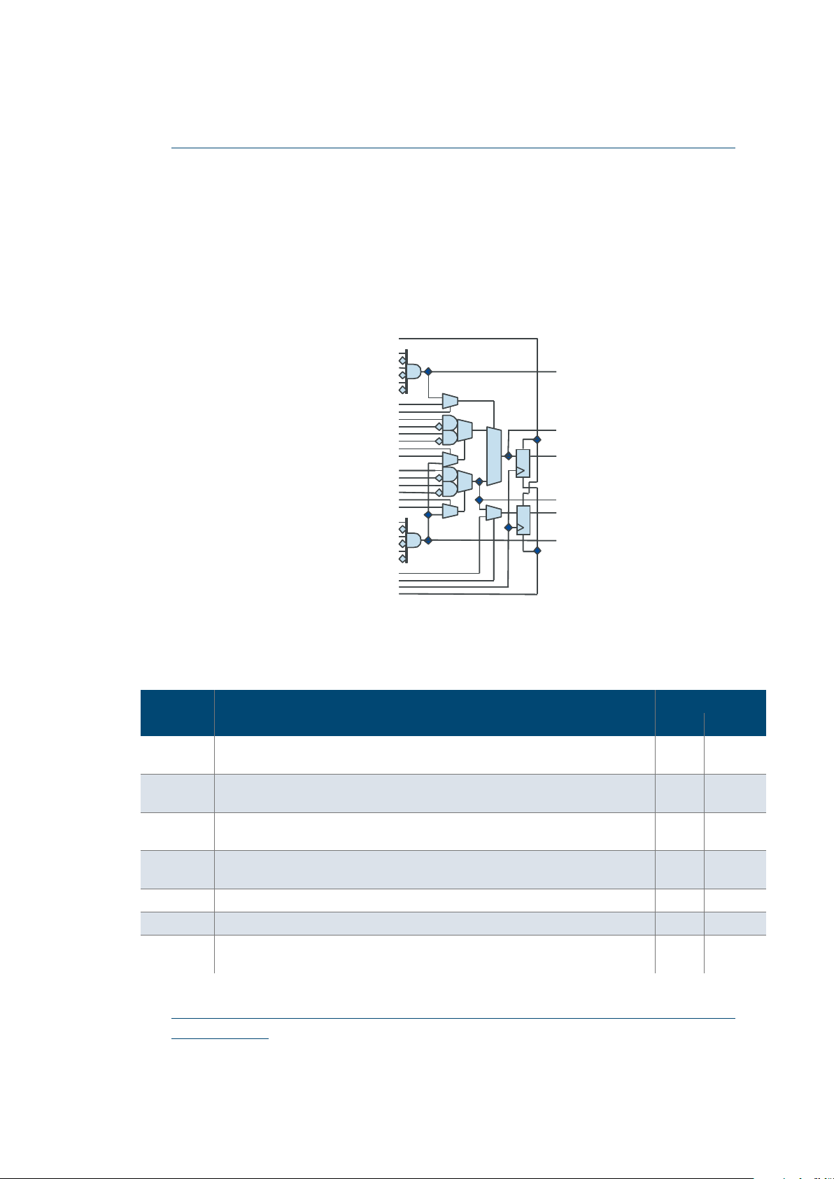
Figure 2: Eclipse-E Logic Cell
Table 1: Logic Cells
Symbol Parameter Value
Logic Cells Min Max
t
PD
Combinatorial Delay of the longest path: time taken by th e combinatorial circuit to
output
- 0.257 ns
t
SU
Setup time: time the synchronous input of the flip-flop must be stable before the
active clock edge
0.22 ns -
t
HL
Hold time: time the synchronous input of the flip-flop must be stable after the active
clock edge
0 ns -
t
CO
Clock-to-out delay: the amount of time taken by the flip-flop to output after the
active clock edge.
- 0.255 ns
t
CWHI
Clock High Time: required minimum time the clock stays high 0.46 ns -
t
CWLO
Clock Low Time: required minimum time that the clock stays low 0.46 ns -
t
SET
Set Delay: time between when the flip-flop is ”set” (high)
and when the output is consequently “set” (high)
- 0.18 ns
Page 3

© 2002 QuickLogic Corporation
www.quicklogic.com
•
•
•
•
•
•
QL6325-E Eclipse-E Data Sheet Rev A
Preliminary
3
Figure 3: Logic Cell Flip-Flop
Figure 4: Logic Cell Flip-Flop Timings—First Waveform
t
RESET
Reset Delay: time between when the flip-flop is ”reset” (low) and when the output
is consequently “reset” (low)
- 0.09 ns
t
SW
Set Width: time that the SET signal remains high/low 0.3 ns -
t
RW
Reset Width: time that the RESET signal remains high/low 0.3 ns -
Table 1: Logic Cells (Continued)
Symbol Parameter Value
Logic Cells Min Max
SET
D
CLK
RESET
Q
SET
RESET
Q
CLK
t
CWHI
(min)
t
CWLO
(min)
t
RESET
t
RW
t
SET
t
SW
Page 4

www.quicklogic.com
© 2002 QuickLogic Corporation
•
•
•
•
•
•
QL6325-E Eclipse-E Data Sheet Rev A
Preliminary
4
Figure 5: Logic Cell Flip-Flop Timings—Second Waveform
Figure 6: Eclipse-E Global Clock Structure
Table 2: Eclipse-E Clock Delay
Clock Source Parameters Clock Performance
Global Dedicated
Logic Cells (Internal) Clock signal generated internally 1.51 ns (max)
Clock Pad Clock signal generated externally 2.06 ns (max) 1.73 ns (max)
CLK
D
Q
t
SU
t
HL
t
CO
Quad net
Page 5
© 2002 QuickLogic Corporation
www.quicklogic.com
•
•
•
•
•
•
QL6325-E Eclipse-E Data Sheet Rev A
Preliminary
5
Figure 7: Global Clock Structure Schematic
Figure 8: RAM Module
Table 3: Eclipse-E Global Clock Delay
Clock Segment Parameter Value
Min Max
t
PGCK
a
a. When using a PLL, t
PGCK
and t
BGCK
are effectively zero due to delay adjustment by
Phase Locked Loop.
Global clock pin delay to quad net - 1.34 ns
t
BGCK
Global clock tree delay (quad net to
flip-flop)
- 0.56 ns
Programmable Clock
External Clock
Global Clock Buffer
Global Clock
t
PGCK
t
BGCK
Clock
Select
WA
WD
WE
WCLK
RE
RCLK
RA
RD
RAM Module
[9:0]
[17:0]
[9:0]
[17:0]
ASYNCRD
Page 6
www.quicklogic.com
© 2002 QuickLogic Corporation
•
•
•
•
•
•
QL6325-E Eclipse-E Data Sheet Rev A
Preliminary
6
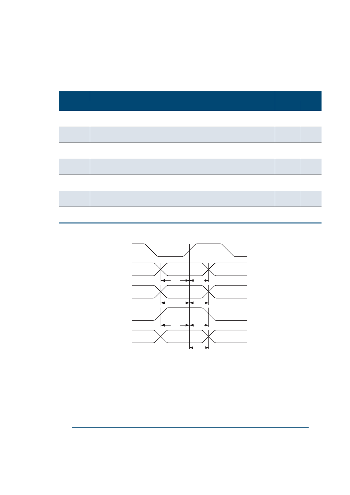
Figure 9: RAM Cell Synchronous Write Timing
Table 4: RAM Cell Synchronous Write Timing
Symbol Parameter Value
RAM Cell Synchronous Write Timing Min Max
t
SWA
WA setup time to WCLK: time the WRITE ADDRESS must be stable before the
active edge of the WRITE CLOCK
0.675 ns -
t
HWA
WA hold t ime to WCLK: time the WRITE ADDRESS must be stable after the active
edge of the WRITE CLOCK
0 ns -
t
SWD
WD setup time to WCLK: time the WRITE DATA must be stable before the active
edge of the WRITE CLOCK
0.654 ns -
t
HWD
WD hold time to WCLK: time the WRITE DA T A must be stable after t he active edge
of the WRITE CLOCK
0 ns -
t
SWE
WE setup time to WCLK: time the WRITE ENABLE must be stable before th e active
edge of the WRITE CLOCK
0.623 ns -
t
HWE
WE hold time to WCLK: time the WRITE ENABLE must be stable after the active
edge of the WRITE CLOCK
0 ns -
t
WCRD
WCLK to RD (WA = RA): time between the active WRITE CLOCK edge and the
time when the data is available at RD
- 4.38 ns
t
SWA
t
SWD
t
SWE
t
HWA
t
HWD
t
HWE
t
WCRD
old data
new data
WCLK
WA
WD
WE
RD
Page 7

© 2002 QuickLogic Corporation
www.quicklogic.com
•
•
•
•
•
•
QL6325-E Eclipse-E Data Sheet Rev A
Preliminary
7
Figure 10: RAM Cell Synchronous & Asynchronous Read Timing
Table 5: RAM Cell Synchronous & Asynchronous Read Timing
Symbol
RAM Cell Synchronous Read Timing Value
Parameter Min Max
t
SRA
RA setup time to RCLK: time the READ ADDRESS must be stable before the active
edge of the READ CLOCK
0.686 ns -
t
HRA
RA hold time to RCLK: time the READ ADDRESS must be stable after the active
edge of the READ CLOCK
0 ns -
t
SRE
RE setup time to WCLK: time the READ ENABLE must be stable before the active
edge of the READ CLOCK
0.243 ns -
t
HRE
RE hold time to WCLK: time the READ ENABLE must be stable after the active
edge of the READ CLOCK
0 ns -
t
RCRD
RCLK to RD: time between the active READ CLOCK edge and the time when the
data is available at RD
- 4.38 ns
RAM Cell Asynchronous Read Timing
r
PDRD
RA to RD: time between when the READ ADDRESS is input and when the DATA
is output
- 2.06 ns
t
SRA
t
HRA
RCLK
RA
t
SRE
t
HRE
t
RCRD
old data
new data
RE
RD
r
PDRD
Page 8

www.quicklogic.com
© 2002 QuickLogic Corporation
•
•
•
•
•
•
QL6325-E Eclipse-E Data Sheet Rev A
Preliminary
8
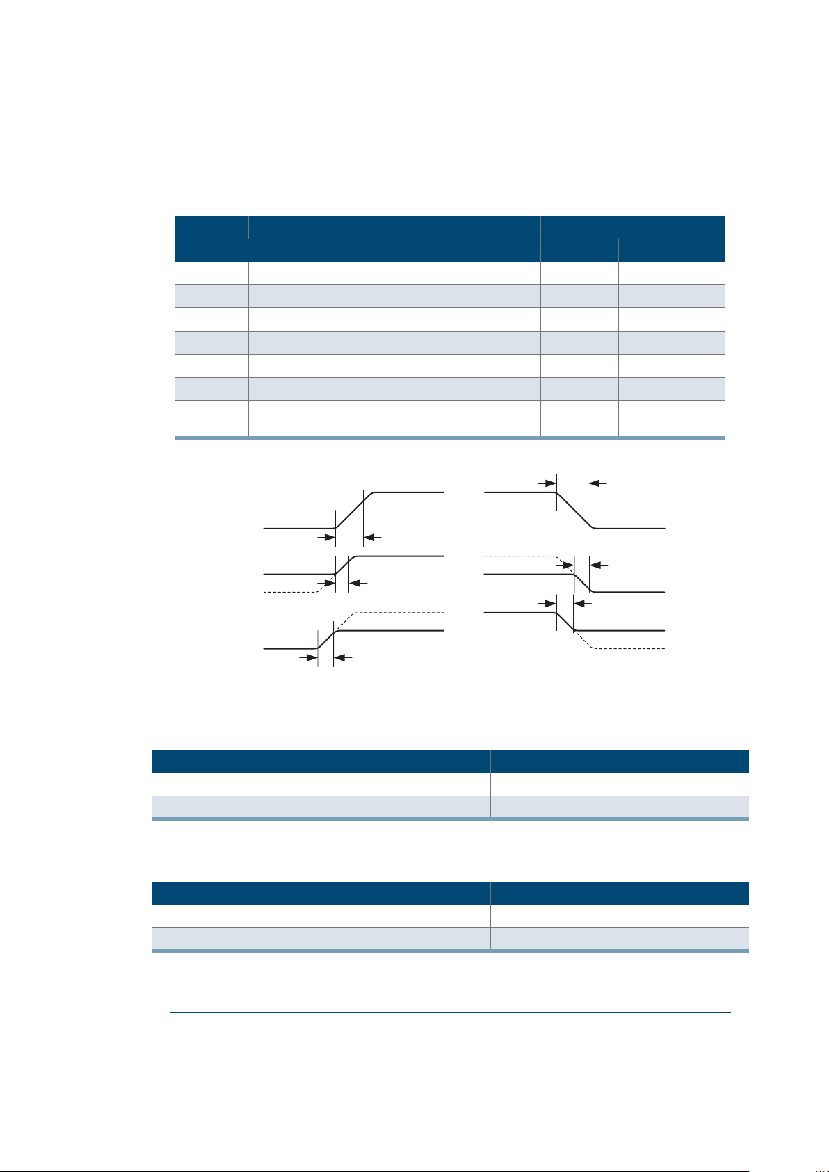
Figure 11: Eclipse-E Cell I/O
Figure 12: Eclipse-E Input Register Cell
E
R
Q
D
R
Q
E
R
Q
D
+
-
PAD
OUTPUT ENABLE
REGISTER
OUTPUT
REGISTER
INPUT
REGISTER
D
PAD
t
ISU
t
SID
+
-
Q
E
D
R
Page 9

© 2002 QuickLogic Corporation
www.quicklogic.com
•
•
•
•
•
•
QL6325-E Eclipse-E Data Sheet Rev A
Preliminary
9
Table 6: Input Register Cell
Symbol Parameter: Input Register Cell Only
Value
Min Max
t
ISU
Input register setup time: the time the synchronous input of the flip-flop must be
stable before the active clock edge
2.50 ns -
t
IHL
Input register hold time: the time the synchronous input of the flip-flop must be
stable after the active clock edge
0 ns -
t
ICO
Input register clock-to-out: the time taken by the flip-flop to output after the active
clock edge
- 1.08 ns
t
IRST
Input register reset delay: the time between when the flip-flop is “reset”(low) and
when the output is consequently “reset” (low)
- 0.99 ns
t
IESU
Input register clock enable setup time: the time “enable” must be stable before the
active clock edge
0.37 ns -
t
IEH
Input register clock enable hold time: the time “enable” must be stable after the
active clock edge
0 ns -
Table 7: Standard Input Delays
Symbol Parameter Value
Standard Input Delays To get the total input delay add this delay to tISU Min Max
t
SID
(LVTTL) LVTTL input delay: Low Voltage TTL for 3.3 V applications - 0.34 ns
t
SID
(LVCMOS2)
LVCMOS2 input delay: Low Voltage CMOS for 2.5 V and lower
applications
- 0.42 ns
t
SID
(LVCMOS18) LVCMOS18 input delay: Low Voltage CMOS for 1.8 V applications - t
SID
(GTL+) GTL+ input delay: Gunning Transceiver Logic - 0.68 ns
t
SID
(SSTL3) SSTL3 input delay: Stub Series Terminated Logic for 3.3 V - 0.55 ns
t
SID
(SSTL2) SSTL2 input delay: Stub Series Terminated Logic for 2.5 V - 0.61 ns
Page 10

www.quicklogic.com
© 2002 QuickLogic Corporation
•
•
•
•
•
•
QL6325-E Eclipse-E Data Sheet Rev A
Preliminary
10
Figure 13: Eclipse-E Input Register Cell Timing
Figure 14: Eclipse-E Output Register Cell
R
CLK
D
Q
ISU IHL
ICO
IESU
IEH
IRST
E
t
t
t
t
t
t
PAD
OUTPUT
REGISTER
Page 11
© 2002 QuickLogic Corporation
www.quicklogic.com
•
•
•
•
•
•
QL6325-E Eclipse-E Data Sheet Rev A
Preliminary
11
Figure 15: Eclipse-E Output Register Cell Timing
Table 8: Eclipse-E Output Register Cell
Symbol Parameter Value
Output Register Cell Only Min Max
t
OUTLH
Output Delay low to high (90% of H) - 0.40 ns
t
OUTHL
Output Delay high to low (10% of L) - 0.55 ns
t
PZH
Output Delay tri-state to high (90% of H) - 2.94 ns
t
PZL
Output Delay tri-state to low (10% of L) - 2.34 ns
t
PHZ
Output Delay high to tri-State - 3.07 ns
t
PLZ
Output Delay low to tri-State - 2.53 ns
t
COP
Clock-to-out delay (does not include clock tree delays) -
3.15 ns (fast slew)
10.2 ns (slow slew)
Table 9: Output Slew Rates @ V
CCIO
= 3.3 V
Fast Slew Slow Slew
Rising Edge 2.8 V/ns 1.0 V/ns
Falling Edge 2.86 V/ns 1.0 V/ns
Table 10: Output Slew Rates @ V
CCIO
= 2.5 V
Fast Slew Slow Slew
Rising Edge 1.7 V/ns 0.6 V/ns
Falling Edge 1.9 V/ns 0.6 V/ns
L
H
L
H
t
OUTLH
t
OUTHL
L
H
Z
t
PZH
L
H
Z
t
PZL
L
H
Z
t
PLZ
L
H
Z
t
PHZ
Page 12

www.quicklogic.com
© 2002 QuickLogic Corporation
•
•
•
•
•
•
QL6325-E Eclipse-E Data Sheet Rev A
Preliminary
12
Table 11: Output Slew Rates @Vccio = 1.8 V
Fast Slew Slow Slew
Rising Edge - V/ns - V/ns
Falling Edge - V/ns - V/ns
Page 13

© 2002 QuickLogic Corporation
www.quicklogic.com
•
•
•
•
•
•
QL6325-E Eclipse-E Data Sheet Rev A
Preliminary
13
DC Characteristics
The DC Specifications are provided in Table 12 through Table 14.
Table 12: Absolute Maximum Ratings
Parameter Value Parameter Value
VCC Voltage -0.5 V to 3.6 V DC Input Current ±20 mA
V
CCIO
Voltage -0.5 V to 4.6 V ESD Pad Protection ±2000 V
INREF Voltage 2.7 V
Leaded Package
Storage Temperature
-65° C to + 150° C
Input V oltage -0.5 V to V
CCIO
+0.5 V
Laminate Package (BGA)
Storage Temperature
-55° C to + 125° C
Latch-up Immunity ±100 mA
Table 13: Operating Range
Symbol Parameter Military Industrial Commercial Unit
Min Max Min Max Min Max
V
CC
Supply Voltage 2.3 2.7 2.3 2.7 2.3 2.7 V
V
CCIO
I/O Input Tolerance Voltage 1.62 3.6 1.62 3.6 1.62 3.6 V
TA Ambient Temperature -55 -40 85 0 70 °C
TC Case Temperature - 125 - - - - °C
K Delay Factor -6 Speed Grade 0.42 1.35 0.43 1.26 0.46 1.23 n/a
-7 Speed Grade 0.42 1.27 0.43 1.19 0.46 1.16 n/a
Table 14: DC Characteristics
Symbol Parameter Conditions Min Max Units
I
I
I or I/O Input Leakage Current VI = V
CCIO
or GND -10 10 µA
I
OZ
3-State Output Leakage Current VI = V
CCIO
or GND -10 10 µA
C
I
Input Capacitance
a
a. Capacitance is sample tested only. Clock pins are 12 pF maximum.
--8pF
I
OS
Output Short Circuit Current
b
b. Only one output at a time. Duration should not exceed 30 seconds.
Vo = GND
V
o
= V
CC
-15
40
-180
210
mA
mA
I
CC
D.C. Supply Current
c
c. For -6/-7 commercial grade devices only. Maximum ICC is 15 mA for
all industrial grade devices, and 25 mA for all military grade devices.
VI,Vo = V
CCIO
or GND - 10 mA
I
CCIO
D.C. Supply Current on V
CCIO
- 0 2 mA
I
CCIO
(DIF)
D.C. Supply Current on V
CCIO
for Differential I/O
---mA
I
REF
D.C. Supply Current on INREF - -10 10 µA
I
PD
Pad Pull-down (programmable) V
CCIO
= 3.6 V - 150 µA
Page 14

www.quicklogic.com
© 2002 QuickLogic Corporation
•
•
•
•
•
•
QL6325-E Eclipse-E Data Sheet Rev A
Preliminary
14
Embedded Computational Unit (ECU)
Traditional Programmable Logic architectures do not implement arithmetic functions efficiently
or effectively—these functions require high logic cell usage while garnering only moderate
performance results.
The QL6325-E architecture allows for functionality above and beyond that achievable using
programmable logic devices. By embedding a dynamically reconfigurable computational unit, the
QL6325-E device can address various arithmetic functions efficiently. This approach offers
greater performance than traditional programmable logic implementations. The embedded block
is implemented at the transistor level as shown in Figure 16.
Figure 16: ECU Block Diagram
The 12 QL6325-E ECU blocks are placed next to the SRAM circuitry for efficient
memory/instruction fetch and addressing for DSP algorithmic implementations.
Twelve 8-bit Multiply-Accumulate (MAC) functions can be implemented per cycle for a total of 1.2
billion MACs when clocked at 100 MHz. Additional MAC functions can be implemented in the
programmable logic.
The modes for the ECU block are dynamically re-programmable through the programmable logic
as shown in Table 15.
A[0:15]
B[0:15]
SIGN2
SIGN1
CIN
S1
S2
S3
A
B
C
D
3-4
decoder
8-bit
Multiplier
17 inc.
COUT
16-bit
Adder
17-bit
Register
2-1
mux
2-1
mux
3-1
mux
Q[0:16]
CLK
RESET
DQ
00
01
10A[0:7]
A[8:15]
Page 15

© 2002 QuickLogic Corporation
www.quicklogic.com
•
•
•
•
•
•
QL6325-E Eclipse-E Data Sheet Rev A
Preliminary
15
Table 15: ECU Mode Select Criteria
TABLE 16.
Instruction
Operation
ECU Performance
a
, -7 WCC
b
a. tPD, tSU and tCO do not include routing paths in/out of the
ECU block.
b. Timing numbers represent -7 Worst Case Commercial
conditions.
S1 S2 S3
t
PD
t
SU
t
CO
0 0 0 Multiply
6.57 ns
max
0 0 1 Multiply-Add
8.84 ns
max
0 1 0 Accumulate
c
c. Internal feedback path in ECU restricts max clk frequency
to 238 MHz.
3.91 ns
min
1.16 ns
max
0 1 1 Add
3.14 ns
max
1 0 0 Multiply (registered)
d
d. B [15:0] set to zero.
9.61 ns
min
1.16 ns
max
1 0 1 Multiply- Add (registered)
9.61 ns
min
1.16 ns
max
1 1 0 Multiply - Accumulate
9.61 ns
min
1.16 ns
max
1 1 1 Add (registered)
3.91 ns
min
1.16 ns
max
Page 16

www.quicklogic.com
© 2002 QuickLogic Corporation
•
•
•
•
•
•
QL6325-E Eclipse-E Data Sheet Rev A
Preliminary
16
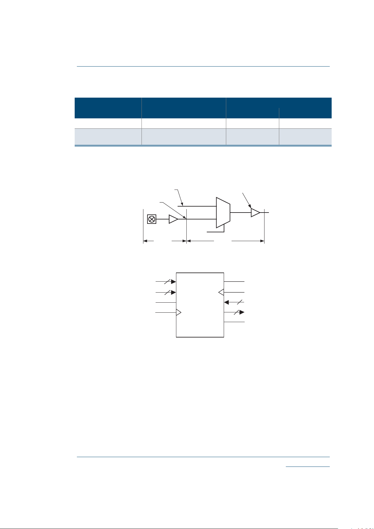
Phase Locked Loops (PLLs)
Instead of requiring extra components, designers simply need to instantiate one of the preconfigured models described in this section and listed in Table . The QuickLogic built-in PLLs
support a wider range of frequencies than many other PLLs. Also, QuickLogic PLLs can be
cascaded to support different ranges of frequency multiplications or divisions, driving the device
at a faster or slower rate than the incoming clock frequency. Most importantly, they achieve a
very short clock-to-out time—generally less than 3 ns. This low clock-to-out time is achieved by
the PLL subtracting the clock tree delay through the feedback path, effectively making the clock
tree delay zero.
Figure 17 illustrates a typical QuickLogic FPGA PLL.
Figure 17: PLL Block
F
in
represents a very stable high-frequency input clock and produces an accurate signal reference.
This signal can either bypass the PLL entirely, thus entering the clock tree directly, or it can pass
through the PLL itself.
Within the PLL, a voltage-controlled oscillator (VCO) is added to the circuit. The external F
in
signal
and the local VCO form a control loop. The VCO is multiplied or divided down to the reference
frequency, so that a phase detector (the crossed circle in Figure 17) can compare the two signals.
If the phases of the external and local signals are not within the tolerance required, the phase
detector sends a signal through the charge pump and loop filter (Figure 17). The charge pump
generates an error voltage to bring the VCO back into alignment and the loop filter removes any
high frequency noise before the error voltage enters the VCO. This new VCO signal enters the
clock tree to drive the chip's circuitry.
F
out
represents the clock signal that emerges from the output pad (the output signal
PLLPAD_OUT is explained in Table 18). This clock signal is meaningful only when the PLL is
configured for external use; otherwise, it remains in high Z state, as shown in the post-simulation
waveform.
vco
Filter
FIN
FOUT
+
-
1st Quadrant
2nd Quadrant
3rd Quadrant
4th Quadrant
Clock
Tree
Frequency Divide
Frequency Multiply
1
.
_
.
2
.
_
.
4
.
_
.
4
.
_
.
2
.
_
.
1
.
.
_
PLL Bypass
Page 17

© 2002 QuickLogic Corporation
www.quicklogic.com
•
•
•
•
•
•
QL6325-E Eclipse-E Data Sheet Rev A
Preliminary
17
Most QuickLogic products contain four PLLs, one to be used in each quadrant. The PLL
presented in Figure 17 controls the clock tree in the fourth Quadrant of its FPGA. As previously
noted, QuickLogic PLLs compensate for the additional delay created by the clock tree itself by
subtracting the clock tree delay through the feedback path.
For more specific information on the Phase Locked Loops, please refer to QuickLogic
Application Note 58.
PLL Modes of Operation
QuickLogic PLLs have eight modes of operation, based on the input frequency and desired output
frequency—Table 17 indicates the features of each mode.
Table 17: PLL Mode Frequencies
PLL Model Output Frequency Input Frequency Range
a
a. The input frequency can range from 16 MHz to 250 MHz, while output frequency ranges from
25 MHz to 250 MHz. When you add PLLs to your top-level design, be sure that the PLL mode
matches your desired input and output frequencies.
Output Frequency Range
PLL_HF
b
b. HF stands for high frequency and LF stands for low frequency.
Same as input frequency 66 MHz–150 MHz 66 MHz–150 MHz
PLL_LF Same as input frequency 25 MHz–133 MHz 25 MHz–133 MHz
PLL_MULT2HF 2 × input frequency 50 MHz–125 MHz 100 MHz–250 MHz
PLL_MULT2LF 2
×
input frequency 16 MHz–50 MHz 32 MHz–100 MHz
PLL_DIV2HF 1/2 × input frequency 100 MHz–250 MHz 50 MHz–125 MHz
PLL_DIV2LF 1/2
×
input frequency 50 MHz–100 MHz 25 MHz–50 MHz
PLL_MULT4 4 × input frequency 16 MHz–40 MHz 64 MHz–160 MHz
PLL_DIV4 1/4
×
input frequency 100 MHz–300 MHz 25 MHz–75 MHz
Page 18

www.quicklogic.com
© 2002 QuickLogic Corporation
•
•
•
•
•
•
QL6325-E Eclipse-E Data Sheet Rev A
Preliminary
18
PLL Signals
Table 18 summarizes the key signals in QuickLogic’s PLLs.
Table 18: PLL Signals
Signal Name Description
PLLCLK_IN
a
a. Because PLLCLK_IN and PLL_RESET signals have INPAD, and
PLLPAD_OUT has OUTP AD, you do not have to add additional pads to your
design
Input clock signal
PLL_RESET
Active High Reset If PLL_RESET is asserted, then CLKNET_OUT and
PLLPAD_OUT are reset to 0. This signal must be asserted and then
released in order for the LOCK_DETECT to work.
ONn_OFFCHIP
PLL output This signal selects whether the PLL will drive the internal
clock network or be used off-chip. This is a static signal, not a dynamic
signal.
Tied to GND = outgoing signal drives internal gates.
Tied to VCC = outgoing signal used off-chip.
CLKNET_OUT
Out to internal gates This signal bypasses the PLL logic before driving
the internal gates. Note that this signal cannot be used in the same
quadrant where the PLL signal is used (PLLCLK_OUT).
PLLCLK_OUT
Out from PLL to internal gates This signal can drive the internal gates
after going through the PLL. For this to work, ONn_OFFCHIP must be
tied to GND.
PLLPAD_OUT
Out to off-chip This outgoing signal is used off-chip. For this to work,
ONn_OFFCHIP signal must be tied to VCC.
LOCK_DETECT
Active High Lock detection signal NOTE: For simulation purposes,
this signal gets asserted after 10 clock cycles. However, it can take a
maximum of 200 clock cycles to sync with the input clock upon release
of the RESET signal.
Table 19: DC Input and Output Levels
a
INREF V
IL
V
IH
V
OL
V
OH
I
OLIOH
V
MINVMAXVMIN
V
MAX
V
MIN
V
MAX
V
MAX
V
MIN
mA mA
LVTTL n/a n/a -0.3 0.8 2.2 V
CCIO
+ 0.3 0.4 2.4 2.0 -2.0
LVCMOS2 n/a n/a -0.3 0.7 1.7 V
CCIO
+ 0.3 0.7 1.7 2.0 -2.0
LVCMOS18 n/a n/a -0.3 0.63 1.2 V
CCIO
+ 0.3 0.7 1.7 2.0 -2.0
GTL+ 0.88 1.12 -0.3 INREF - 0.2 INREF + 0.2 V
CCIO
+ 0.3 0.6 n/a 40 n/a
PCI n/a n/a -0.3 0.3 x V
CCIO
0.5 x V
CCIO
V
CCIO
+ 0.5 0.1 x V
CCIO
0.9 x V
CCIO
1.5 -0.5
SSTL2 1.15 1.35 -0.3 INREF - 0.18 INREF + 0.18 V
CCIO
+ 0.3 0.74 1.76 7.6 -7.6
SSTL3 1.3 1.7 -0.3 INREF
- 0.2 INREF + 0.2 V
CCIO
+ 0.3 1.10 1.90 8 -8
Page 19

© 2002 QuickLogic Corporation
www.quicklogic.com
•
•
•
•
•
•
QL6325-E Eclipse-E Data Sheet Rev A
Preliminary
19
NOTE:
All CLK and IOCTRL pins are clamped to the V
ded
rail. Therefore, these pins can be
driven up to V
ded
+ 0.3 V.
Package Thermal Characteristics
Thermal Resistance Equations:
θ
JC
= (TJ - TC)/P
θ
JA
= (TJ - TA)/P
P
MAX
= (T
JMAX
- T
AMAX
)/
θ
JA
Parameter Description:
θ
JC
: Junction-to-case thermal resistance
θ
JA
: Junction-to-ambient thermal resistance
T
J
: Junction temperature
T
A
: Ambient temperature
P: Power dissipated by the device while operating
P
MAX
: The maximum power dissipation for the device
T
JMAX
: Maximum junction temperature
T
AMAX
: Maximum ambient temperature
NOTE:
Maximum junction temperature (T
JMAX
) is 150º C. To calculate the maximum power
dissipation for a device package look up
θ
JA
from Table 20, pick an appropriate T
AMAX
and use:
P
MAX
= (150º C - T
AMAX
)/
θ
JA
a. The data provided in Table 19 are JEDEC and PCI Specifications. QuickLogic devices ei-
ther meet or exceed these requirements. See preceding Table 1 through Table 14 and
Figure 1 through Figure 17 for data specific to QuickLogic I/Os.
Table 20: Package Thermal Characteristics
Package Description θJA (º C/W) @ various flow rates (m/sec) θ
JC
(º C/W)
Pin Count Package Type 0 0.5 1 2
484 PBGA 28.0 26.0 25.0 23.0 9.0
280 LF-PBGA 18.5 17.0 15.5 14.0 7.0
208 PQFP 26.0 24.5 23.0 22.0 11.0
Page 20

www.quicklogic.com
© 2002 QuickLogic Corporation
•
•
•
•
•
•
QL6325-E Eclipse-E Data Sheet Rev A
Preliminary
20
Kv and Kt Graphs
Figure 18: Voltage Factor vs. Supply Voltage
Figure 19: Te mperature Factor vs. Operating Temperature
Voltage Factor vs. Supply Voltage
0.9200
0.9400
0.9600
0.9800
1.0000
1.0200
1.0400
1.0600
1.0800
1.1000
2.25 2.3 2.35 2.4 2.45 2.5 2.55 2.6 2.65 2.7 2.75
Supply Voltage (V)
Kv
Temperatur e Factor vs. Operating Temperature
0.85
0.90
0.95
1.00
1.05
1.10
1.15
-60 -40 -20 0 20 40 60 80
Junction Temperature C
Kt
Page 21

© 2002 QuickLogic Corporation
www.quicklogic.com
•
•
•
•
•
•
QL6325-E Eclipse-E Data Sheet Rev A
Preliminary
21
Power vs. Operating Frequency
The basic power equation which best models power consumption is given below:
P
TOTAL
= 0.350 + f[0.0031
η
LC
+ 0.0948
η
CKBF
+ 0.01
η
CLBF
+ 0.0263
η
CKLD
+
0.543
η
RAM
+ 0.20
η
PLL
+ 0.0035
η
INP
+ 0.0257
η
OUTP
] (mW)
Where
•
η
LC
is the total number of logic cells in the design
•
η
CKBF
= # of clock buffers
•
η
CLBF
= # of column clock buffers
•
η
CKLD
= # of loads connected to the column clock buffers
•
η
RAM
= # of RAM blocks
•
η
PLL
= # of PLLs
•
η
INP
is the number of input pins
•
η
OUTP
is the number of output pins
NOTE:
To learn more about power consumption, please refer to Application Note #60.
Page 22

www.quicklogic.com
© 2002 QuickLogic Corporation
•
•
•
•
•
•
QL6325-E Eclipse-E Data Sheet Rev A
Preliminary
22
Power-up Sequencing
Figure 20: Power-up Requirements
The following requirements must be met when powering up a device (refer to Figure 20):
•
When ramping up the power supplies keep (V
CCIO
-VCC)
MAX
≤ 500 mV . Deviation from this
recommendation can cause permanent damage to the device.
•
V
CCIO
must lead VCC when ramping the device.
•
The power supply must be greater than or equal to 400 µs to reach VCC. Ramping to
V
CC/VCCIO
before reaching 400 µs can cause the device to behave improperly.
Voltage
V
CCIO
V
CC
(V
CCIO
-VCC)
MAX
400 us
V
CC
Page 23

© 2002 QuickLogic Corporation
www.quicklogic.com
•
•
•
•
•
•
QL6325-E Eclipse-E Data Sheet Rev A
Preliminary
23
Joint Test Access Group (JTAG)
Figure 21: JTAG Block Diagram
Microprocessors and Application Specific Integrated Circuits (ASICs) pose many design
challenges, one problem being the accessibility of test points. The Joint Test Access Group (JT AG)
formed in response to this challenge, resulting in IEEE standard 1149.1, the Standard T est Access
Port and Boundary Scan Architecture.
The JTAG boundary scan test methodology allows complete observation and control of the
boundary pins of a JTAG-compatible device through JTAG software. A Test Access Port (TAP)
controller works in concert with the Instruction Register (IR), which allow users to run three
required tests along with several user-defined tests.
JTAG tests allow users to reduce system debug time, reuse test platforms and tools, and reuse
subsystem tests for fuller verification of higher level system elements.
TCK
TMS
TRSTB
RDI
TDO
Instruction Decode
&
Control Logic
TAp Controller
State Machine
(16 States)
Instruction Register
Boundary-Scan Register
(Data Register)
Mux
Bypass
Register
Mux
Internal
Register
I/O Registers
User Defined Data Register
Page 24

www.quicklogic.com
© 2002 QuickLogic Corporation
•
•
•
•
•
•
QL6325-E Eclipse-E Data Sheet Rev A
Preliminary
24
The 1149.1 standard requires the following three tests:
•
Extest Instruction. The Extest instruction performs a PCB interconnect test. This test
places a device into an external boundary test mode, selecting the boundary scan register to
be connected between the T AP's T est Data In (TDI) and T est Data Out (TDO) pins. Boundary
scan cells are preloaded with test patterns (via the Sample/Preload Instruction), and input
boundary cells capture the input data for analysis.
•
Sample/Preload Instruction. This instruction allows a device to remain in its functional
mode, while selecting the boundary scan register to be connected between the TDI and TDO
pins. For this test, the boundary scan register can be accessed via a data scan operation,
allowing users to sample the functional data entering and leaving the device.
•
Bypass Instruction. The Bypass instruction allows data to skip a device's boundary scan
entirely, so the data passes through the bypass register. The Bypass instruction allows users
to test a device without passing through other devices. The bypass register is connected
between the TDI and TDO pins, allowing serial data to be transferred through a device
without affecting the operation of the device.
Page 25

© 2002 QuickLogic Corporation
www.quicklogic.com
•
•
•
•
•
•
QL6325-E Eclipse-E Data Sheet Rev A
Preliminary
25
Pin Descriptions
Figure 22: I/O Banks with Relevant Pins
Table 21: JTAG Pin Descriptions
Pin Function Description
TDI/RSI
Test Data In for JTAG/RAM
init. Serial Data In
Hold HIGH during normal operation. Connects to serial PROM
data in for RAM initialization. Connect to V
CC
if unused
TRSTB/RRO
Active low Reset for
JTAG/RAM init. reset out
Hold LOW during normal operation. Connects to serial PROM
reset for RAM initialization. Connect to GND if unused
TMS Test Mode Select for JTAG
Hold HIGH during normal operation. Connect to V
CC
if not used
for JTAG
TCK Test Clock for JTAG
Hold HIGH or LOW during normal operation. Connect to VCC or
ground if not used for JTAG
TDO/RCO
Test data out for JTAG/RAM
init. clock out
Connect to serial PROM clock for RAM initialization. Must be left
unconnected if not used for JTAG or RAM initialization
IO BANK A IO BANK B
V
CCIO
(A)
INREF(A)
IOCTRL(A)
IO(A)
V
CCIO
(A)
INREF(A)
IOCTRL(A)
IO(A)
IO BANK C IO BANK D
V
CCIO
(C)
INREF(C)
IOCTRL(C)
IO(C)
V
CCIO
(D)
INREF(D)
IOCTRL(D)
IO(D)
IO BANK F IO BANK E
V
CCIO
(F)
INREF(F)
IOCTRL(F)
IO(F)
V
CCIO
(E)
INREF(E)
IOCTRL(E)
IO(E)
IO BANK HIO BANK G
(H)
INREF(H)
IOCTRL(H)
IO(H)
V
CCIO
V
CCIO
(G)
INREF(G)
IOCTRL(G)
IO(G)
Page 26

www.quicklogic.com
© 2002 QuickLogic Corporation
•
•
•
•
•
•
QL6325-E Eclipse-E Data Sheet Rev A
Preliminary
26
Table 22: Dedicated Pin Descriptions
Pin Function Description
GCLK Global clock network driver
Low skew global clock. This pin provides access to a dedicated,
distributed network capable of driving the CLOCK, SET, RESET,
F1, and A2 inputs to the Logic Cell, READ, and WRITE CLOCKS,
Read and Write Enables of the Embedded RAM Blocks, CLOCK
of the ECUs, and Output Enables of the I/Os.
I/O(A) Input/Output pin
The I/O pin is a bi-directional pin, configurable to either an inputonly, output-only, or bi-directional pin. The A inside the
parenthesis means that the I/O is located in Bank A. If an I/O is
not used, SpDE (QuickWorks Tool) provides the option of tying
that pin to GND, V
CC,
or TriState during programming.
V
CC
Power supply pin Connect to 2.5 V supply
V
CCIO
(A) Input voltage tolerance pin
This pin provides the flexibility to interface the device with either a
3.3 V , 2.5 V , or 1.8 V device. The A inside the parenthesis means
that V
CCIO
is located in BANK A. Every I/O pin in Bank A will be
tolerant of V
CCIO
input signals and will output V
CCIO
level signals.
This pin must be connected to either 3.3 V, 2.5 V, or 1.8 V.
GND Ground pin Connect to ground
PLLIN PLL clock input Clock input for PLL
DEDCLK Dedicated clock pin
Low skew global clock. This pin provides access to a dedicated,
distributed clock network capable of driving the CLOCK inputs of
all sequential elements of the device (e.g. RAM, Flip Flops).
GNDPLL Ground pin for PLL Connect to GND
INREF(A) Differential reference voltage
The INREF is the reference voltage pin for GTL+, SSTL2, and
STTL3 standards. Follow the recommendations provided in
Table 19
for the appropriate standard. The A inside the
parenthesis means that INREF is located in BANK A. This pin
should be tied to GND if not needed.
PLLOUT PLL output pin Dedicated PLL output pin; otherwise, may be left unconnected
IOCTRL(A) Highdrive input
This pin provides fast RESET , SET, CLOCK, and ENABLE access
to the I/O cell flip-flops, providing fast clock-to-out and fast I/O
response times. This pin can also double as a high-drive pin to the
internal logic cells. The A inside the parenthesis means that
IOCTRL is located in Bank A. There is an internal pulldown
resistor to Ground on this pin. This pin should be tied to Ground if
it is not used. For backwards compatibility with Eclipse, it can be
tied to Vcc or Ground. If tied to Vcc, it will draw no more than
20 µA per IOCTRL pin due to the pulldown resistor.
(Sheet 1 of 2)
Page 27

© 2002 QuickLogic Corporation
www.quicklogic.com
•
•
•
•
•
•
QL6325-E Eclipse-E Data Sheet Rev A
Preliminary
27
Vpump Charge Pump Disable
This pin disables the internal charge pump for lower static power
operation. T o disable the charge pump, connect Vpump to 3.3 V.
If the Disable Charge Pump feature is not used, connect Vpump to
Ground. For backwards compatibility with Eclipse and EclipsePlus
devices, connect Vpump to Ground.
Vded
Voltage tolerance for clocks,
JTAG, and IOCTRL/V oltage
Drive for PLLOUT and JTAG
pins
This pin specifies the input voltage tolerance for CLK, JT AG, and
IOCTRL dedicated input pins, as well as the output voltage drive
for PLLOUT and JTAG pins. If the PLLs are used, Vded must be
the same as V
CC
PLL. For backwards compatibility with Eclipse and
EclipsePlus devices, connect Vded to 2.5 V.
VccPLL Power Supply pin for PLL
Connect to 2.5 V supply or 3.3 V supply. For backwards
compatibility with Eclipse and EclipsePlus devices, connect to
2.5 V.
Table 22: Dedicated Pin Descriptions
Pin Function Description
(Sheet 2 of 2)
Page 28

www.quicklogic.com
© 2002 QuickLogic Corporation
•
•
•
•
•
•
QL6325-E Eclipse-E Data Sheet Rev A
Preliminary
28
Recommended Unused Pin Terminations for the Eclipse-E
Devices
All unused, general purpose I/O pins can be tied to VCC, GND, or HIZ (high impedance) internally
using the Configuration Editor. This option is given in the bottom-right corner of the placement
window. T o use the Placement Editor, choose Constraint
>
Fix Placement in the Option pull-
down menu of SpDE.
The rest of the pins should be terminated at the board level in the manner presented in Table 23.
208 PQFP Pinout Diagram
Table 23: Recommended Unu sed Pin Terminations
Signal Name Recommended Termination
PLLOUT<x>
a
a. x represents a number.
Unused PLL output pins must be connected to either VCC or GND so that their associated
input buffer never floats. Utilized PLL output pins that route the PLL clock outside of the
chip should not be tied to either V
CC
or GND.
IOCTRL<y>
b
b. y represents an aphabetical character.
Any unused pins of this type must be connected to either VCC or GND.
CLK/PLLIN<x> Any unused clock pins should be connected to V
CC
or GND.
PLLRST<x>
If a PLL module is not used, then the associated PLLRST<x> must be connected to VCC,
under normal operation use it as needed.
INREF<y>
If an I/O bank does not require the use of INREF signal the pin should be connected to
GND.
Eclipse-E
QL6325-E-6PQ208C
Page 29

© 2002 QuickLogic Corporation
www.quicklogic.com
•
•
•
•
•
•
QL6325-E Eclipse-E Data Sheet Rev A
Preliminary
29
208 PQFP Pinout Table
Table 24: 208 PQFP Pinout Table
PQFP Function PQFP Function PQFP Function PQFP Function PQFP Function
1
PLLRST(3)
43
IO(B)
85
IO(D)
127
CLK(5),PLLIN(3)
169
IOCTRL(G)
2
V
CCPLL
(3)
44
V
CCIO
(B)
86
V
CC
128
CLK(6)
170
INREF(G)
3
GND
45
IO(B)
87
IO(D)
129
Vded
171
IOCTRL(G)
4
GND
46
V
CC
88
IO(D)
130
CLK(7)
172
IO(G)
5
IO(A)
47
IO(B)
89
V
CC
131
V
CC
173
IO(G)
6
IO(A)
48
IO(B)
90
IO(D)
132
CLK(8)
174
IO(V)
7
IO(A)
49
GND
91
IO(D)
133
TMS
175
V
CC
8
V
CCIO
(A)
50
TDO
92
IOCTRL(D)
134
IO(F)
176
IO(G)
9
IO(A)
51
PLLOUT(1)
93
INREF(D)
135
IO(F)
177
V
CCIO
(G)
10
IO(A)
52
GNDPLL(2)
94
IOCTRL(D)
136
IO(F)
178
GND
11
IOCTRL(A)
53
GND
95
IO(D)
137
GND
179
IO(G)
12
V
CC
54
V
CCPLL
(2)
96
IO(D)
138
V
CCIO
(F)
180
IO(G)
13
INREF(A)
55
PLLRST(2)
97
IO(D)
139
IO(F)
181
IO(G)
14
IOCTRL(A)
56
V
CC
98
V
CCIO
(D)
140
IO(F)
182
V
CC
15
IO(A)
57
IO(C)
99
IO(D)
141
IO(F)
183
TCK
16
IO(A)
58
GND
100
IO(D)
142
IO(F)
184
V
CC
17
IO(A)
59
IO(C)
101
Vpump
143
IO(F)
185
IO(H)
18
IO(A)
60
V
CCIO
(C)
102
PLLOUT(0)
144
IOCTRL(F)
186
IO(H)
19
V
CCIO
(A)
61
IO(C)
103
GND
145
INREF(F)
187
IO(H)
20
IO(A)
62
IO(C)
104
GNDPLL(1)
146
V
CC
188
GND
21
GND
63
IO(C)
105
PLLRST(1)
147
IOCTRL(F)
189
V
CCIO
(H)
22
IO(A)
64
IO(C)
106
V
CCPLL
(1)
148
IO(F)
190
IO(H)
23
TDI
65
IO(C)
107
IO(E)
149
IO(F)
191
IO(H)
24
CLK(0)
66
IO(C)
108
GND
150
V
CCIO
(F)
192
IOCTRL(H)
25
CLK(1)
67
IOCTRL(C)
109
IO(E)
151
IO(F)
193
IO(H)
26
V
CC
68
INREF(C)
110
IO(E)
152
IO(F)
194
INREF(H)
27
CLK(2),PLLIN(2)
69
IOCTRL(C)
111
V
CCIO
(E)
153
GND
195
V
CC
28
CLK(3),PLLIN(1)
70
IO(C)
112
IO(E)
154
IO(F)
196
IOCTRL(H)
29
Vded
71
IO(C)
113
V
CC
155
PLLOUT(3)
197
IO(H)
30
CLK(4),
DEDCLK,PLLIN(0)
72
V
CCIO
(C)
114
IO(E)
156
GNDPLL(0)
198
IO(H)
31
IO(B)
73
IO(C)
115
IO(E)
157
GND
199
IO(H)
32
IO(B)
74
IO(C)
116
IO(E)
158
V
CCPLL
(0)
200
IO(H)
33
GND
75
GND
117
IOCTRL(E)
159
PLLRST(0)
201
IO(H)
34
V
CCIO
(B)
76
V
CC
118
INREF(E)
160
GND
202
IO(H)
35
IO(B)
77
IO(C)
119
IOCTRL(E)
161
IO(G)
203
V
CCIO
(H)
36
IO(B)
78
TRSTB
120
IO(E)
162
V
CCIO
(G)
204
GND
37
IO(B)
79
V
CC
121
IO(E)
163
IO(G)
205
IO(H)
38
IO(B)
80
IO(D)
122
V
CCIO
(E)
164
IO(G)
206
PLLOUT(2)
39
IOCTRL(B)
81
IO(D)
123
GND
165
V
CC
207
GND
40
INREF(B)
82
IO(D)
124
IO(E)
166
IO(G)
208
GNDPLL(3)
41
IOCTRL(B)
83
GND
125
IO(E)
167
IO(G)
42
IO(B)
84
V
CCIO
(D)
126
IO(E)
168
IO(G)
Page 30

www.quicklogic.com
© 2002 QuickLogic Corporation
•
•
•
•
•
•
QL6325-E Eclipse-E Data Sheet Rev A
Preliminary
30
280 PBGA Pinout Diagram
Top
Bottom
Eclipse-E
QL6325-E-6PT280C
Pin A1
Corner
Page 31

© 2002 QuickLogic Corporation
www.quicklogic.com
•
•
•
•
•
•
QL6325-E Eclipse-E Data Sheet Rev A
Preliminary
31
280 PBGA Pinout Table
Table 25: 280 PBGA Pinout Table
PBGA Function PBGA Function PBGA Function PBGA Function PBGA Function PBGA Function
A1
PLLOUT<3>
C10
CLK<5>
/PLLIN<3>
E19
IOCTRL<D>
K16
I/O<C>
R4
I/O<H>
U13
I/O<B>
A2
GNDPLL<0>
C11
V
CCIO
<E>
F1
INREF<G>
K17
I/O<D>
R5
GND
U14
IOCTRL<B>
A3
I/O<F>
C12
I/O<E>
F2
IOCTRL<G>
K18
I/O<C>
R6
GND
U15
V
CCIO
<B>
A4
I/O<F>
C13
I/O<E>
F3
I/O<G>
K19
TRSTB
R7
V
CC
U16
I/O<B>
A5
I/O<F>
C14
I/O<E>
F4
I/O<G>
L1
I/O<H>
R8
V
CC
U17
TDO
A6
IOCTRL<F>
C15
V
CCIO
<E>
F5
GND
L2
I/O<H>
R9
GND
U18
PLLRST<2>
A7
I/O<F>
C16
I/O<E>
F15
V
CC
L3
V
CCIO
<H>
R10
GND
U19
I/O<B>
A8
I/O<F>
C17
I/O<E>
F16
IOCTRL<D>
L4
I/O<H>
R11
V
CC
V1
PLLOUT<2>
A9
I/O<F>
C18
I/O<E>
F17
I/O<D>
L5
V
CC
R12
V
CC
V2
GNDPLL<3>
A10
CLK<7>
C19
I/O<E>
F18
I/O<D>
L15
GND
R13
V
CC
V3
GND
A11
I/O<E>
D1
I/O<G>
F19
I/O<D>
L16
I/O<C>
R14
Vded
V4
I/O<A>
A12
I/O<E>
D2
I/O<G>
G1
I/O<G>
L17
V
CCIO
<C>
R15
GND
V5
I/O<A>
A13
I/O<E>
D3
I/O<F>
G2
I/O<G>
L18
I/O<C>
R16
I/O<C>
V6
IOCTRL<A>
A14
IOCTRL<E>
D4
I/O<F>
G3
IOCTRL<G>
L19
I/O<C>
R17
V
CCIO
<C>
V7
I/O<A>
A15
I/O<E>
D5
I/O<F>
G4
I/O<G>
M1
I/O<H>
R18
I/O<C>
V8
I/O<A>
A16
I/O<E>
D6
I/O<F>
G5
V
CC
M2
I/O<H>
R19
I/O<C>
V9
I/O<A>
A17
I/O<E>
D7
I/O<F>
G15
V
CC
M3
I/O<H>
T1
I/O<H>
V10
CLK<1>
A18
PLLRST<1>
D8
I/O<F>
G16
I/O<D>
M4
I/O<H>
T2
I/O<H>
V11
CLK<4>
DEDCLK/PLLIN<0>
A19
GND
D9
CLK<8>
G17
I/O<D>
M5
V
CC
T3
I/O<A>
V12
I/O<B>
B1
PLLRST<0>
D10
I/O<E>
G18
I/O<D>
M15
V
CC
T4
I/O<A>
V13
I/O<B>
B2
GND
D11
I/O<E>
G19
I/O<D>
M16
INREF<C>
T5
I/O<A>
V14
INREF<B>
B3
I/O<F>
D12
I/O<E>
H1
I/O<G>
M17
I/O<C>
T6
IOCTRL<A>
V15
I/O<B>
B4
I/O<F>
D13
INREF<E>
H2
I/O<G>
M18
I/O<C>
T7
I/O<A>
V16
I/O<B>
B5
I/O<F>
D14
I/O<E>
H3
I/O<G>
M19
I/O<C>
T8
I/O<A>
V17
I/O<B>
B6
INREF<F>
D15
I/O<E>
H4
I/O<G>
N1
IOCTRL<H>
T9
I/O<A>
V18
GNDPLL<2>
B7
I/O<F>
D16
I/O<D>
H5
V
CC
N2
I/O<H>
T10
I/O<A>
V19
GND
B8
I/O<F>
D17
I/O<D>
H15
V
CC
N3
I/O<H>
T11
CLK<3>
/PLLIN<1>
W1
GND
B9
TMS
D18
I/O<D>
H16
V
CC
N4
I/O<H>
T12
I/O<B>
W2
PLLRST<3>
B10
CLK<6>
D19
I/O<D>
H17
I/O<D>
N5
V
CC
T13
I/O<B>
W3
I/O<A>
B11
I/O<E>
E1
I/O<G>
H18
I/O<D>
N15
V
CC
T14
I/O<B>
W4
I/O<A>
B12
I/O<E>
E2
I/O<G>
H19
I/O<D>
N16
I/O<C>
T15
I/O<B>
W5
I/O<A>
B13
IOCTRL<E>
E3
V
CCIO
<G>
J1
I/O<G>
N17
I/O<C>
T16
I/O<B>
W6
I/O<A>
B14
I/O<E>
E4
I/O<F>
J2
I/O<G>
N18
IOCTRL<C>
T17
V
CCPLL
<2>
W7
I/O<A>
B15
I/O<E>
E5
GND
J3
V
CCIO
<G>
N19
IOCTRL<C>
T18
I/O<B>
W8
I/O<A>
B16
I/O<E>
E6
V
CC
J4
I/O<G>
P1
I/O<H>
T19
I/O<B>
W9
TDI
B17
V
CCPLL
<1>
E7
V
CC
J5
GND
P2
I/O<H>
U1
I/O<A>
W10
CLK<2>
/PLLIN<2>
B18
GNDPLL<1>
E8
Vded
J15
V
CC
P3
IOCTRL<H>
U2
I/O<A>
W11
I/O<B>
B19
PLLOUT<0>
E9
V
CC
J16
I/O<C>
P4
INREF<H>
U3
V
CCPLL
<3>
W12
I/O<B>
C1
I/O<F>
E10
GND
J17
V
CCIO
<D>
P5
V
CC
U4
I/O<A>
W13
I/O<B>
C2
V
CCPLL
<0>
E11
GND
J18
I/O<D>
P15
GND
U5
V
CCIO
<A>
W14
IOCTRL<B>
C3
I/O<F>
E12
V
CC
J19
I/O<D>
P16
I/O<C>
U6
INREF<A>
W15
I/O<B>
C4
I/O<F>
E13
V
CC
K1
V
CC
P17
I/O<C>
U7
I/O<A>
W16
I/O<B>
C5
V
CCIO
<F>
E14
GND
K2
TCK
P18
I/O<C>
U8
I/O<A>
W17
I/O<B>
C6
IOCTRL<F>
E15
Vpump
K3
I/O<G>
P19
I/O<C>
U9
V
CCIO
<A>
W18
I/O<B>
C7
I/O<F>
E16
I/O<D>
K4
I/O<G>
R1
I/O<H>
U10
CLK<0>
W19
PLLOUT<1>
C8
I/O<F>
E17
V
CCIO
<D>
K5
GND
R2
I/O<H>
U11
V
CCIO
<B>
C9
V
CCIO
<F>
E18
INREF<D>
K15
GND
R3
V
CCIO
<H>
U12
I/O<B>
Page 32

www.quicklogic.com
© 2002 QuickLogic Corporation
•
•
•
•
•
•
QL6325-E Eclipse-E Data Sheet Rev A
Preliminary
32
484 PBGA Pinout Diagram
Top
Bottom
Eclipse-E
QL6325-E-6PS484C
20 19 18 17 16 15 14 13 12 11 10 9 8 7 6 5 4 3 2 1
A
B
C
E
D
F
G
H
K
J
L
M
N
R
P
T
U
V
Y
W
22 21
AB
AA
Pin A1
Corner
Pin A1
Page 33

© 2002 QuickLogic Corporation
www.quicklogic.com
•
•
•
•
•
•
QL6325-E Eclipse-E Data Sheet Rev A
Preliminary
33
484 PBGA Pinout Table
Table 26: 484 PBGA Pinout Table
PBGA Function PBGA Function PBGA Function PBGA Function PBGA Function PBGA Function
A1
I/O<A>
C1
I/O<A>
E1
IOCTRL<A>
G1
I/O<A>
J1
I/O<A>
L1
CLK<4>
DEDCLK/PLLIN<0>
A2
PLLRST<3>
C2
I/O<A>
E2
I/O<A>
G2
I/O<A>
J2
I/O<A>
L2
CLK<0>
A3
I/O<A>
C3
V
CCPLL
<3>
E3
I/O<A>
G3
I/O<A>
J3
I/O<A>
L3
CLK<2>/PLLIN<2>
A4
I/O<A>
C4
PLLOUT<2>
E4
I/O<A>
G4
I/O<A>
J4
I/O<A>
L4
I/O<A>
A5
I/O<A>
C5
I/O<A>
E5
I/O<A>
G5
I/O<A>
J5
I/O<A>
L5
I/O<A>
A6
I/O<H>
C6
I/O<H>
E6
I/O<H>
G6
I/O<A>
J6
I/O<A>
L6
I/O<A>
A7
I/O<H>
C7
I/O<H>
E7
N/C
G7
GND
J7
I/O<A>
L7
GND
A8
IOCTRL<H>
C8
I/O<H>
E8
I/O<H>
G8
I/O<H>
J8
V
CC
L8
GND
A9
I/O<H>
C9
IOCTRL<H>
E9
I/O<H>
G9
I/O<H>
J9
GND
L9
GND
A10
N/C
C10
I/O<H>
E10
I/O<H>
G10
I/O<H>
J10
V
CC
L10
GND
A11
N/C
C11
I/O<H>
E11
V
CC
G11
I/O<G>
J11
V
CC
L11
GND
A12
TCK
C12
I/O<H>
E12
I/O<G>
G12
GND
J12
GND
L12
GND
A13
I/O<G>
C13
I/O<G>
E13
I/O<G>
G13
I/O<G>
J13
V
CC
L13
GND
A14
I/O<G>
C14
I/O<G>
E14
I/O<G>
G14
I/O<G>
J14
GND
L14
V
CC
A15
I/O<G>
C15
I/O<G>
E15
IOCTRL<G>
G15
I/O<G>
J15
V
CC
L15
V
CC
A16
I/O<G>
C16
I/O<G>
E16
I/O<G>
G16
Vpump
J16
I/O<F>
L16
CLK<6>
A17
I/O<G>
C17
I/O<G>
E17
INREF<G>
G17
V
CCIO
<F>
J17
V
CCIO
<F>
L17
V
CCIO
<F>
A18
I/O<G>
C18
I/O<G>
E18
I/O<G>
G18
I/O<F>
J18
I/O<F>
L18
I/O<F>
A19
I/O<F>
C19
I/O<F>
E19
I/O<F>
G19
I/O<F>
J19
I/O<F>
L19
CLK<8>
A20
GND
C20
GNDPLL<0>
E20
I/O<F>
G20
I/O<F>
J20
I/O<F>
L20
I/O<F>
A21
PLLOUT<3>
C21
I/O<F>
E21
I/O<F>
G21
INREF<F>
J21
I/O<F>
L21
I/O<F>
A22
I/O<F>
C22
I/O<F>
E22
I/O<F>
G22
I/O<F>
J22
I/O<F>
L22
I/O<F>
B1
I/O<A>
D1
I/O<A>
F1
I/O<A>
H1
I/O<A>
K1
TDI
M1
I/O<B>
B2
GND
D2
I/O<A>
F2
INREF<A>
H2
I/O<A>
K2
I/O<A>
M2
I/O<B>
B3
GNDPLL<3>
D3
I/O<A>
F3
I/O<A>
H3
I/O<A>
K3
I/O<A>
M3
I/O<B>
B4
GND
D4
I/O<A>
F4
I/O<A>
H4
I/O<A>
K4
I/O<A>
M4
CLK<3>/PLLIN<1>
B5
I/O<A>
D5
I/O<A>
F5
I/O<A>
H5
IOCTRL<A>
K5
I/O<A>
M5
I/O<B>
B6
I/O<H>
D6
I/O<H>
F6
V
CCIO
<A>
H6
V
CCIO
<A>
K6
V
CCIO
<A>
M6
V
CCIO
<B>
B7
I/O<H>
D7
I/O<H>
F7
V
CCIO
<H>
H7
I/O<H>
K7
I/O<A>
M7
CLK<1>
B8
INREF<H>
D8
I/O<H>
F8
I/O<H>
H8
GND
K8
V
CC
M8
V
CC
B9
I/O<H>
D9
I/O<H>
F9
V
CCIO
<H>
H9
V
CC
K9
V
CC
M9
V
CC
B10
I/O<H>
D10
I/O<H>
F10
I/O<H>
H10
V
CC
K10
GND
M10
GND
B11
I/O<H>
D11
I/O<H>
F11
V
CCIO
<H>
H11
V
ded
K11
GND
M11
GND
B12
N/C
D12
I/O<G>
F12
V
CCIO
<G>
H12
GND
K12
GND
M12
GND
B13
N/C
D13
I/O<G>
F13
I/O<G>
H13
V
CC
K13
GND
M13
GND
B14
N/C
D14
I/O<G>
F14
V
CCIO
<G>
H14
V
CC
K14
V
CC
M14
GND
B15
I/O<G>
D15
IOCTRL<G>
F15
N/C
H15
GND
K15
V
CC
M15
GND
B16
I/O<G>
D16
I/O<G>
F16
V
CCIO
<G>
H16
I/O<F>
K16
I/O<F>
M16
GND
B17
I/O<G>
D17
I/O<G>
F17
N/C
H17
I/O<F>
K17
I/O<F>
M17
I/O<E>
B18
I/O<G>
D18
I/O<F>
F18
I/O<F>
H18
I/O<F>
K18
I/O<F>
M18
I/O<E>
B19
PLLRST<0>
D19
V
CCPLL
<0>
F19
I/O<F>
H19
I/O<F>
K19
I/O<F>
M19
I/O<E>
B20
I/O<F>
D20
I/O<F>
F20
IOCTRL<F>
H20
I/O<F>
K20
I/O<F>
M20
CLK<7>
B21
I/O<F>
D21
I/O<F>
F21
I/O<F>
H21
I/O<F>
K21
I/O<F>
M21
CLK<5>/PLLIN<3>
B22
I/O<F>
D22
I/O<F>
F22
IOCTRL<F>
H22
I/O<F>
K22
I/O<F>
M22
TMS
(Sheet 1 of 2)
Page 34

www.quicklogic.com
© 2002 QuickLogic Corporation
•
•
•
•
•
•
QL6325-E Eclipse-E Data Sheet Rev A
Preliminary
34
N1
I/O<B>
P16
I/O<E>
T9
N/C
V2
I/O<B>
W17
I/O<D>
AA10
I/O<C>
N2
I/O<B>
P17
I/O<E>
T10
TRSTB
V3
I/O<B>
W18
I/O<E>
AA11
I/O<C>
N3
I/O<B>
P18
I/O<E>
T11
GND
V4
I/O<B>
W19
I/O<E>
AA12
I/O<D>
N4
I/O<B>
P19
I/O<E>
T12
N/C
V5
I/O<B>
W20
I/O<E>
AA13
I/O<D>
N5
I/O<B>
P20
I/O<E>
T13
I/O<D>
V6
I/O<C>
W21
I/O<E>
AA14
I/O<D>
N6
I/O<B>
P21
I/O<E>
T14
N/C
V7
I/O<C>
W22
I/O<E>
AA15
I/O<D>
N7
I/O<B>
P22
I/O<E>
T15
I/O<D>
V8
I/O<C>
Y1
I/O<B>
AA16
I/O<D>
N8
V
CC
R1
I/O<B>
T16
GND
V9
N/C
Y2
I/O<B>
AA17
I/O<D>
N9
V
CC
R2
INREF<B>
T17
I/O<E>
V10
I/O<C>
Y3
V
CCPLL
<2>
AA18
I/O<D>
N10
GND
R3
I/O<B>
T18
I/O<E>
V11
I/O<C>
Y4
I/O<C>
AA19
I/O<E>
N11
GND
R4
I/O<B>
T19
I/O<E>
V12
V
CC
Y5
I/O<C>
AA20
GNDPLL<1>
N12
GND
R5
I/O<B>
T20
I/O<E>
V13
N/C
Y6
I/O<C>
AA21
I/O<E>
N13
GND
R6
I/O<B>
T21
IOCTRL<E>
V14
I/O<D>
Y7
I/O<C>
AA22
I/O<E>
N14
V
CC
R7
I/O<B>
T22
I/O<E>
V15
I/O<D>
Y8
IOCTRL<C>
AB1
I/O<B>
N15
V
CC
R8
GND
U1
IOCTRL<B>
V16
INREF<D>
Y9
I/O<C>
AB2
GNDPLL<2>
N16
I/O<E>
R9
V
CC
U2
I/O<B>
V17
I/O<D>
Y10
I/O<C>
AB3
PLLRST<2>
N17
V
CCIO
<E>
R10
V
CC
U3
IOCTRL<B>
V18
I/O<E>
Y11
I/O<D>
AB4
I/O<B>
N18
I/O<E>
R11
GND
U4
I/O<B>
V19
I/O<E>
Y12
I/O<D>
AB5
I/O<B>
N19
I/O<E>
R12
Vded
U5
I/O<B>
V20
I/O<E>
Y13
I/O<D>
AB6
I/O<C>
N20
I/O<E>
R13
V
CC
U6
I/O<C>
V21
I/O<E>
Y14
I/O<D>
AB7
I/O<C>
N21
I/O<E>
R14
V
CC
U7
V
CCIO
<C>
V22
I/O<E>
Y15
IOCTRL<D>
AB8
IOCTRL<C>
N22
I/O<E>
R15
GND
U8
N/C
W1
I/O<B>
Y16
I/O<D>
AB9
I/O<C>
P1
I/O<B>
R16
I/O<D>
U9
V
CCIO
<C>
W2
I/O<B>
Y17
I/O<D>
AB10
I/O<C>
P2
I/O<B>
R17
V
CCIO
<E>
U10
I/O<C>
W3
I/O<B>
Y18
I/O<E>
AB11
I/O<C>
P3
I/O<B>
R18
I/O<E>
U11
V
CCIO
<C>
W4
I/O<B>
Y19
PLLOUT<0>
AB12
I/O<D>
P4
I/O<B>
R19
I/O<E>
U12
V
CCIO
<D>
W5
I/O<B>
Y20
PLLRST<1>
AB13
I/O<D>
P5
I/O<B>
R20
I/O<E>
U13
I/O<D>
W6
I/O<C>
Y21
I/O<E>
AB14
I/O<D>
P6
V
CCIO
<B>
R21
I/O<E>
U14
V
CCIO
<D>
W7
N/C
Y22
I/O<E>
AB15
I/O<D>
P7
I/O<B>
R22
I/O<E>
U15
N/C
W8
I/O<C>
AA1
TDO
AB16
IOCTRL<D>
P8
V
CC
T1
I/O<B>
U16
V
CCIO
<D>
W9
I/O<C>
AA2
PLLOUT<1>
AB17
I/O<D>
P9
GND
T2
I/O<B>
U17
V
CCIO
<E>
W10
I/O<C>
AA3
GND
AB18
I/O<D>
P10
V
CC
T3
I/O<B>
U18
I/O<E>
W11
I/O<C>
AA4
I/O<B>
AB19
I/O<E>
P11
GND
T4
I/O<B>
U19
I/O<E>
W12
I/O<D>
AA5
I/O<C>
AB20
GND
P12
V
CC
T5
I/O<B>
U20
IOCTRL<E>
W13
I/O<D>
AA6
I/O<C>
AB21
V
CCPLL
<1>
P13
V
CC
T6
V
CCIO
<B>
U21
I/O<E>
W14
I/O<D>
AA7
I/O<C>
AB22
I/O<E>
P14
GND
T7
GND
U22
INREF<E>
W15
I/O<D>
AA8
INREF<C>
P15
V
CC
T8
I/O<C>
V1
I/O<B>
W16
N/C
AA9
I/O<C>
Table 26: 484 PBGA Pinout Table (Continued)
PBGA Function PBGA Function PBGA Function PBGA Function PBGA Function PBGA Function
(Sheet 2 of 2)
Page 35

© 2002 QuickLogic Corporation
www.quicklogic.com
•
•
•
•
•
•
QL6325-E Eclipse-E Data Sheet Rev A
Preliminary
35
Ordering Information
Figure 23: Ordering Information
Contact Information
Telephone: 408 990 4000 (US)
416 497 8884 (Canada)
44 1932 57 9011 (Europe)
49 89 930 86 170 (Germany)
852 8106 9091 (Asia)
81 45 470 5525 (Japan)
E-mail: info@quicklogic.com
Support: support@quicklogic.com
Web site: http://www.quicklogic.com/
Revision History
Table 27: Revision History
Revision Date Comments
A
December
2002
Brian Faith, Andreea Rotaru
QL 6325-E - 6 PQ208 C
QuickLogic device
Eclipse-E device
part number
Speed Grade
6 = Faster
7 = Fastest
Operating Range
C = Commercial
I = Industrial
M = Military
Package Code
PQ208 = 208-pin PQFP
PT280 = 280-pin FPBGA (0.8 mm)
PS484 = 484-pin BGA (1.0 mm)
Page 36

www.quicklogic.com
© 2002 QuickLogic Corporation
•
•
•
•
•
•
QL6325-E Eclipse-E Data Sheet Rev A
Preliminary
36
Copyright and Trademark Information
Copyright © 2002 QuickLogic Corporation.
All Rights Reserved.
The information contained in this document and the accompanying software programs is
protected by copyright. All rights are reserved by QuickLogic Corporation. QuickLogic
Corporation reserves the right to modify this document without any obligation to notify any
person or entity of such revision. Copying, duplicating, selling, or otherwise distributing any part
of this product without the prior written consent of an authorized representative of QuickLogic is
prohibited.
QuickLogic and the QuickLogic logo, pASIC, Vi aLink, DeskFab, and Q uickW orks are registered
trademarks of QuickLogic Corporation; Eclipse, QuickFC, QuickDSP, QuickDR, QuickSD,
QuickT ools, QuickCore, QuickPro, SpDE, WebASIC, and W ebESP are trademarks of QuickLogic
Corporation.
 Loading...