

QUICK LOGIC QL4016-0CF100M, QL4016-0CG84M, QL4016-1CG84M, QL4016-1PL84M, QL4016-0PL84M Datasheet
...
90,000 Usable PLD Gate QuickRAM Combining Performance, Density and Embedded RAM
Military QuickRAM
D
Device Highlights
Military QuickRAM
EVICE HIGHLIGHTS
Features
F
EATURES
High Performance and High Density
■ Up to 90,000 Usable PLD Gates with 316 I/Os
■ 300 MHz 16-bit Counters, 400 MHz Datapaths, 160+
MHz FIFOs
■ 0.35um four-layer metal non-volatile CMOS process for
smallest die sizes
High Speed Embedded SRAM
■ Up to 22 dual-port RAM modules, organized in user-
configurable 1,152-bit blocks
■ 5ns access times, each port independently accessible
■ Fast and efficient for FIFO, RAM, and ROM functions
Easy to Use / Fast Development Cycles
■ 100% routable with 100% utilization and complete
pin-out stability
■ Variable-grain logic cells provide high performance and
100% utilization
■ Comprehensive design tools include high quality Verilog/
VHDL synthesis
Advanced I/O Capabilities
■ Interfaces with both 3.3 volt and 5.0 volt devices
■ PCI compliant with 3.3V and 5.0V buses for -1/-2
speed grades
■ Full JTAG boundary scan
■ Registered I/O cells with individually controlled clocks
and output enables
Total of 316 I/O pins
■ 308 bi-directional input/output pins, PCI-compliant for
5.0 volt and 3.3 volt buses for -1/-2/-3/-4 speed grades
■ 8 high-drive input/distributed network pins
Eight Low-Skew Distributed Networks
■ Two array clock/control networks available to the logic
cell flip-flop clock, set and reset inputs - each driven by
an input-only pin
■ Six global clock/control networks available to the logic
cell F1, clock, set and reset inputs and the input and I/O
register clock, reset and enable inputs as well as the
output enable control - each driven by an input-only or
I/O pin, or any logic cell output or I/O cell feedback
High Performance
■ Input + logic cell + output total delays under 6 ns
■ Data path speeds exceeding 400 MHz
■ Counter speeds over 300 MHz
■ FIFO speeds over 160+ MHz
Military Reliability
■ Mil-STD-883 and Miil Temp Ceramic
■ Mil Temp Plastic - Guaranteed -55°C to 125°C
Device
QL4016
11,520 RAM Bits
QL4036
16,128 RAM bits
QL4090
25,344 RAM bits
M = Military T e mperatu re (-1 5 to +125 degrees C)
/888 = MIL STD 883
Usable
Gates
8,000-
16,000
16,000-
25,000
36,00060,000
Package
84CPGA
84PLCC
100CQFP
144CPGA
208PQFP
208CQFP
208PQFP
208CQFP
240PQFP
256CPGA
456PBGA
TABLE 1: Selector Table
Rev A
Max
I/O
70
70
82
118
174
174
174
174
207
223
316
Qualificatio n
Level
M, /883
M
M, /883
M, /883
M
M, /883
M
M, /883
M
M, /883
M
Supply
Voltage
3.3 V
3.3 V
3.3 V
3.3 V
3.3 V
3.3 V
3.3V
3.3V
3.3V
3.3V
3.3V
8-37
P
Product Summary
Military QuickRAM
RODUCT SUMMARY
The QuickRAM family of ESPs (Embedded Standard
Products) offers FPGA logic in combination with
Dual-Port SRAM modules. QuickRAM is a 90,000
usable PLD gate ESPs. QuickRAM ESPs are fabricated on a 0.35mm four-layer metal process using
QuickLogic’s patented ViaLink technology to provide
a unique combination of high performance, high
density, low cost, and extreme ease-of-use.
QuickRAM contains up to 1,584 logic cells and 22
dual port RAM modules. Each RAM module has
1,152 RAM bits, for a total of up to 25,344 bits.
RAM Modules are Dual Port (one read port, one
write port) and can be configured into one of four
modes: 64 (deep) x18 (wide), 128x9, 256x4, or
512x2. With a maximum of 316 I/Os, and is avail-
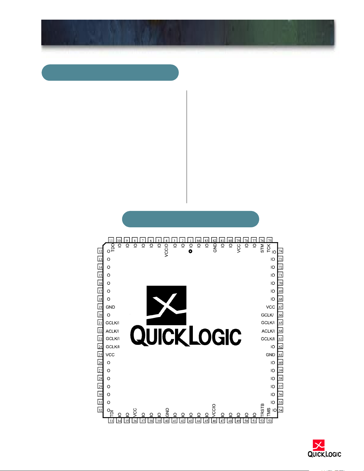
Pinout Diagram 84-Pin PLCC
P
INOUT DIAGRAM
able in plastic 84-PLCC, 208-PQFP, 240-PQFP and
456-PBGA packages and in ceramic 100, 208CQFP and 84, 144, 256-CPGA.
Software support for the complete QuickRAM family
is available through two basic packages. The turnkey
QuickWorks
ESP software solution from design entry to logic synthesis, to place and route, to simulation. The Quick-
TM
Tools
for designers who use Cadence, Exemplar, Mentor,
Synopsys, Synplicity, Viewlogic, Veribest, or other
third-party tools for design entry, synthesis, or simulation.
package provides the most complete
for Workstations package provides a solution
84-PIN PLCC
QuickRAM
QL4016-1PL84M
TABLE 2: 84-pin PLCC
8-38
38 Preliminary
Rev A

Pin #1
Military QuickRAM
P
INOUT DIAGRAM
Pinout Diagram 100-Pin CQFP
QuickRAM
QL4016-1CF100M
100-PIN CQFP
Pin #76
Pin #26
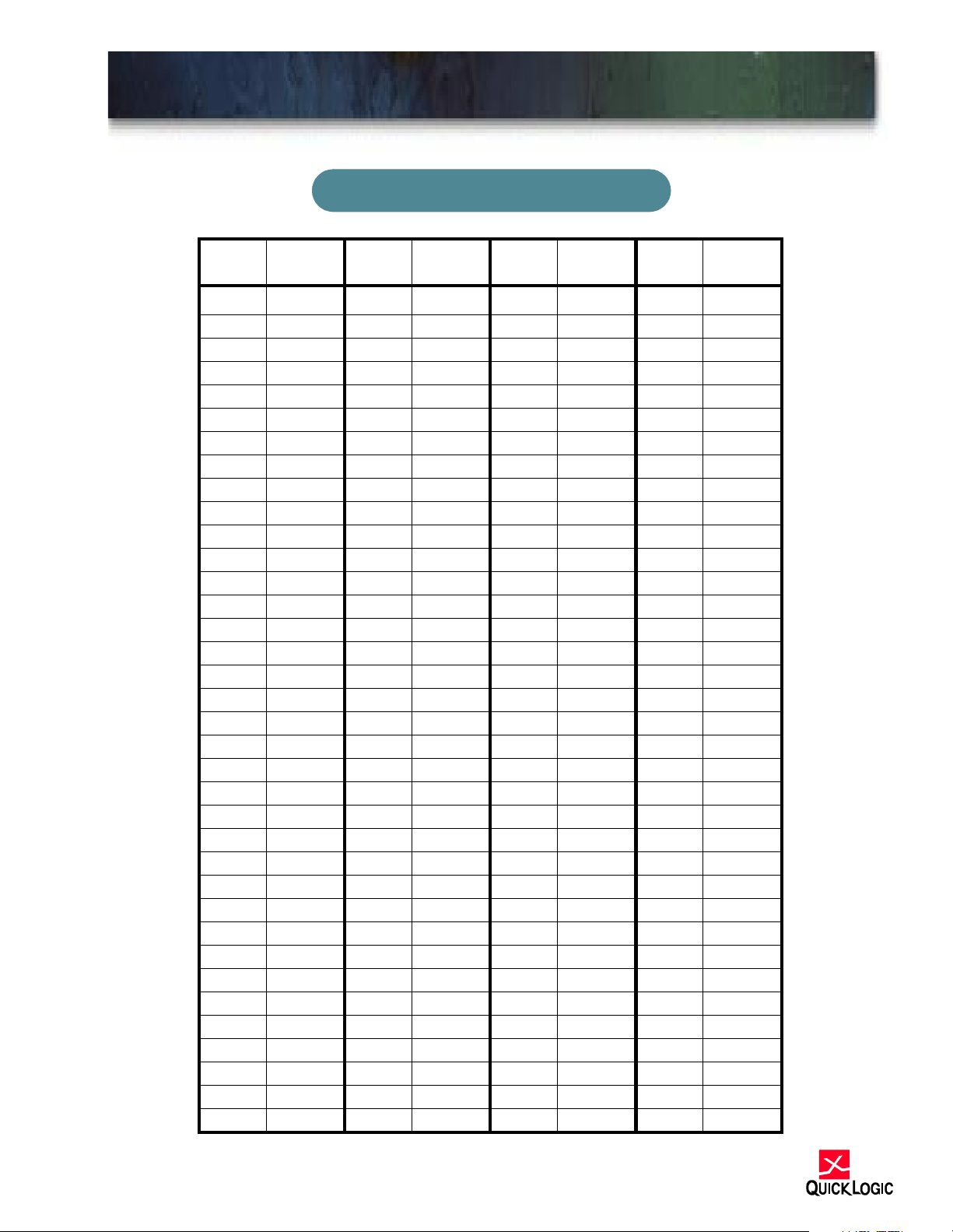
100 CQFP Pinout Table
100
Function
TQFP
1 I/O 26 TDI 51 I/O 76 TCK
2 I/O 27 I/O 52 I/O 77 STM
3 I/O 28 I/O 53 I/O 78 I/O
4 I/O 29 I/O 54 I/O 79 I/O
5 I/O 30 I/O 55 I/O 80 I/O
6 I/O 31 I/O 56 I/O 81 I/O
7 I/O 32 I/O 57 I/O 82 I/O
8 I/O 33 I/O 58 I/O 83 I/O
9 GND 34 I/O 59 GND 84 I/O
10 I/O 35 GND 60 I/O 85 GND
11 GCLK / I 36 I/O 61 GCLK / I 86 I/O
12 ACLK / I 37 I/O 62 ACLK / I 87 I/O
13 VCC 38 GND 63 VCC 88 GND
14 GCLK / I 39 I/O 64 GCLK / I 89 I/O
15 GCLK / I 40 I/O 65 GCLK / I 90 I/O
16 VCC 41 I/O 66 VCC 91 I/O
17 I/O 42 VCCIO 67 I/O 92 VCCIO
18 I/O 43 I/O 68 I/O 93 I/O
19 I/O 44 I/O 69 I/O 94 I/O
20 I/O 45 I/O 70 I/O 95 I/O
21 I/O 46 I/O 71 I/O 96 I/O
22 I/O 47 I/O 72 I/O 97 I/O
23 I/O 48 I/O 73 I/O 98 I/O
24 I/O 49 TRSTB 74 I/O 99 I/O
25 I/O 50 TMS 75 I/O 100 TDO
100
TQFP
Function
100
TQFP
Function
100
TQFP
Function
Pin #51
Rev A
8-39

Military QuickRAM
P
INOUT DIAGRAMS
208-Pin PQFP/CQFP
Pin #1
Pin #53
Pin #1
Pin #157
QuickRAM
QL4090-1PQ208M
Pin #105
240-Pin PQFP
Pin #157
QuickRAM
QL4090-1PQ240M
Pin #53
8-40
40 Preliminary
Rev A
Pin #105

Military QuickRAM
P
INOUT TABLE
P
INOUT TABLE
PQFP/CQFP 240/208 Pinout Table
240 208 Function 240 208 Function 240 208 Function 240 208 Function 240 208 Function
PQFP PQFP PQFP PQFP PQFP PQFP PQFP PQFP PQFP PQFP
1 208 I/O 51 43 GND 98 84 I/O 145 125 I/O 194 168 I/O
2 1 I/O 52 44 I/O 99 85 I/O 146 126 I/O 195 169 I/O
3 2 I/O 53 45 I/O 100 86 I/O 147 127 GND 196 NC I/O
4 3 I/O 54 46 I/O 101 87 I/O 148 128 I/O 197 170 I/O
5 4 I/O 55 47 I/O 102 88 I/O 149 NC I/O 198 171 I/O
6 5 I/O 56 48 I/O 103 89 I/O 150 129 GCLK / I 199 172 I/O
7 NC I/O 57 NC I/O 104 90 I/O 151 130 ACLK / I 200 173 I/O
8 6 I/O 58 49 I/O 105 91 I/O 152 131 VCC 201 174 I/O
9 7 I/O 59 50 I/O 106 92 I/O 153 132 GCLK / I 202 175 I/O
10 8 I/O 60 51 I/O 107 NC I/O 154 133 GCLK / I 203 NC I/O
11 9 I/O NC 52 I/O 108 93 I/O 155 134 VCC 204 176 I/O
12 10 VCC NC 53 I/O 109 94 I/O 156 135 I/O 205 177 GND
13 11 I/O 61 54 TDI 110 95 GND 157 136 I/O 206 178 I/O
14 12 GND 62 NC I/O NC 96 I/O 158 NC I/O 207 179 I/O
15 13 I/O 63 NC I/O 111 97 VCC 159 137 I/O 208 NC I/O
16 14 I/O 64 55 I/O NC 98 I/O 160 NC GND 209 180 I/O
17 NC I/O 65 56 I/O NC 99 I/O 161 138 I/O 210 181 I/O
18 15 I/O 66 NC I/O 112 100 I/O 162 139 I/O 211 182 GND
19 16 I/O 67 57 I/O 113 NC I/O 163 140 I/O 212 NC VCC
20 17 I/O 68 58 I/O 114 101 I/O 164 141 I/O 213 183 I/O
21 18 I/O 69 59 GND 115 NC I/O 165 142 I/O 214 184 I/O
22 19 I/O 70 60 I/O 116 102 I/O 166 NC I/O 215 185 I/O
23 20 I/O 71 61 VCC 117 NC I/O 167 143 I/O 216 186 I/O
24 NC I/O 72 62 I/O 118 NC I/O 168 144 I/O 217 187 VCCIO
25 21 I/O 73 63 I/O 119 103 TRSTB 169 145 VCC 218 188 I/O
26 22 I/O 74 64 I/O 120 104 TMS 170 NC I/O 219 NC I/O
27 23 GND 75 NC I/O 121 105 I/O 171 146 I/O 220 189 I/O
28 24 I/O 76 65 I/O 122 NC I/O 172 147 GND 221 190 I/O
29 25 GCLK / I 77 66 I/O 123 106 I/O 173 148 I/O 222 191 I/O
30 26 ACLK / I 78 67 I/O 124 107 I/O 174 149 I/O 223 192 I/O
31 27 VCC 79 NC I/O 125 108 I/O 175 150 I/O 224 193 I/O
32 28 GCLK / I 80 68 I/O 126 109 I/O 176 151 I/O 225 194 I/O
33 29 GCLK / I 81 69 I/O 127 NC I/O 177 152 I/O 226 NC I/O
34 30 VCC 82 70 I/O 128 110 I/O 178 153 I/O 227 195 I/O
35 31 I/O 83 NC I/O 129 111 I/O 179 154 I/O 228 196 I/O
36 32 I/O NC 71 I/O 130 112 I/O 180 155 I/O 229 197 I/O
37 NC GND 84 NC I/O 131 113 I/O NC 156 I/O 230 198 I/O
38 33 I/O 85 72 I/O 132 114 VCC 181 157 TCK 231 NC I/O
39 NC I/O 86 73 GND 133 115 I/O 182 158 STM 232 199 GND
40 34 I/O 87 74 I/O 134 116 GND 183 NC I/O 233 200 I/O
41 35 I/O 88 NC VCC 135 117 I/O 184 159 I/O 234 201 VCC
42 36 I/O 89 75 I/O 136 NC I/O 185 160 I/O 235 202 I/O
43 NC I/O 90 76 I/O 137 118 I/O 186 161 I/O 236 203 I/O
44 37 I/O 91 77 I/O 138 119 I/O 187 162 I/O 237 204 I/O
45 38 I/O 92 78 GND 139 120 I/O 188 163 GND 238 205 I/O
46 39 I/O 93 79 I/O 140 121 I/O 189 164 I/O 239 206 I/O
47 NC I/O 94 80 I/O 141 NC I/O 190 165 VCC 240 207 TDO
48 40 I/O 95 81 I/O 142 122 I/O 191 166 I/O
49 41 VCC 96 82 I/O 143 123 I/O 192 NC I/O
50 42 I/O 97 83 VCCIO 144 124 I/O 193 167 I/O
Rev A
8-41

Pinout Diagram 84-Pin CPGA
P
QuickRAM
QL4016-1CG84M
Military QuickRAM
INOUT DIAGRAM
84-PIN CPGA
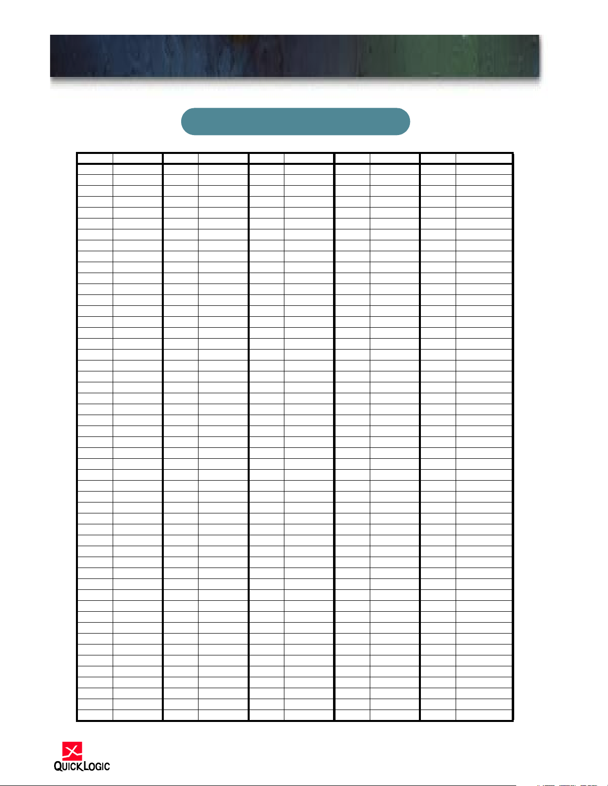
84-Pin CPGA Pinout Table
84 CPGA Function 84 CPGA Function 84 CPGA Function 84 CPGA Function
A1 I/O B11 I/O F9 I/O K2 I/O
A2 I/O C1 VCC F10 I/O K3 I/O
A3 I/O C2 I/O F11 I/O K4 I/O
A4 I/O C5 VCC G1 I/O K5 GCLK / I
A5 I/O C6 ACLK / I G2 I/O K6 GCLK / I
A6 I/O C7 GND G3 VCCIO K7 GCLK / I
A7 I/O C10 I/O G9 GND K8 I/O
A8 I/O C11 I/O G10 I/O K9 I/O
A9 I/O D1 I/O G11 I/O K10 TCK
A10 I/O D2 I/O H1 I/O K11 I/O
A11 TDO D10 I/O H2 I/O L1 TMS
B1 I/O D11 I/O H10 VCC L2 I/O
B2 TDI E1 I/O H11 I/O L3 I/O
B3 I/O E2 I/O J1 I/O L4 I/O
B4 I/O E3 GND J2 TRSTB L5 I/O
B5 GCLK / I E9 VCCIO J5 GND L6 I/O
B6 GCLK / I E10 I/O J6 ACLK / I L7 I/O
B7 GCLK / I E11 I/O J7 VCC L8 I/O
B8 I/O F1 I/O J10 STM L9 I/O
B9 I/O F2 I/O J11 I/O L10 I/O
B10 I/O F3 I/O K1 I/O L1 1 I/O
8-42
Rev A
42 Preliminary

Pinout Diagrams 144 & 256-Pin CPGAs
QuickRAM
QL4036-1CG144M
Military QuickRAM
P
INOUT DIAGRAMS
144 & 256-PIN CPGA
S
QuickRAM
QL4090-1CG256M
144-Pin CPGA
1 2 3 4 5 6 7 8 9 10 11 12 13 14 15 16 17 18 19 20
Y
W
V
U
T
R
P
N
M
L
K
J
H
G
F
E
D
C
B
A
256-Pin CPGA
Rev A
8-43
Pinout Table 144-Pin CPGA
Military QuickRAM
P
INOUT TABLE
144-PIN CPGA
144
CPGA
A1 I/O C7 I/O H13 ACLK / I N10 I/O
A2 I/O C8 GND H14 I/O N11 GND
A3 I/O C9 I/O H15 GCLK / I N12 I/O
A4 I/O C10 I/O J1 GCLK / I N13 I/O
A5 I/O C11 I/O J2 VCC N14 I/O
A6 I/O C12 TCK J3 VCC N15 I/O
A7 I/O C13 I/O J13 I/O P1 I/O
A8 I/O C14 I/O J14 I/O P2 I/O
A9 I/O C15 I/O J15 GND P3 TDI
A10 GND D1 I/O K1 GCLK / I P4 I/O
A11 I/O D2 I/O K2 I/O P5 I/O
A12 I/O D3 I/O K3 I/O P6 I/O
A13 VCC D13 I/O K13 I/O P7 I/O
A14 I/O D14 I/O K14 I/O P8 I/O
A15 I/O D15 I/O K15 I/O P9 VCCIO
B1 I/O E1 I/O L1 I/O P10 I/O
B2 TDO E2 VCC L2 I/O P11 I/O
B3 I/O E3 I/O L3 GND P12 I/O
B4 I/O E13 GND L13 I/O P13 I/O
B5 I/O E14 I/O L14 VCC P14 TRSTB
B6 I/O E15 I/O L15 I/O P15 I/O
B7 VCCIO F1 I/O M1 I/O R1 I/O
B8 I/O F2 I/O M2 I/O R2 I/O
B9 I/O F3 I/O M3 I/O R3 VCC
B10 I/O F13 I/O M13 I/O R4 I/O
B11 I/O F14 I/O M14 I/O R5 I/O
B12 I/O F15 GCLK / I M15 I/O R6 GND
B13 STM G1 GND N1 I/O R7 I/O
B14 I/O G2 I/O N2 I/O R8 I/O
B15 I/O G3 I/O N3 I/O R9 I/O
C1 I/O G13 VCC N4 I/O R10 I/O
C2 I/O G14 VCC N5 I/O R11 I/O
C3 I/O G15 GCLK / I N6 I/O R12 I/O
C4 I/O H1 GCLK / I N7 I/O R13 I/O
C5 GND H2 I/O N8 GND R14 I/O
C6 I/O H3 ACLK / I N9 I/O R15 TMS
Function
144
CPGA
Function
144
CPGA
Function
144
CPGA
Function
8-44
44 Preliminary
Rev A

Military QuickRAM
P
INOUT TABLE
Pinout Table 256-Pin CPGA
256
CPGA
Function
A1 VCC C4 I/O E19 I/O L2 GCLK / I T17 I/O V20 I/O
A2 I/O C5 I/O E20 VCC L3 GND T18 I/O W1 I/O
A3 VCC C6 I/O F1 I/O L4 I/O T19 I/O W2 I/O
A4 I/O C7 I/O F2 GND L17 GCLK / I T20 I/O W3 I/O
A5 I/O C8 I/O F3 I/O L18 I/O U1 I/O W4 I/O
A6 I/O C9 I/O F4 I/O L19 VCC U2 I/O W5 GND
A7 I/O C10 I/O F17 I/O L20 ACLK / I U3 I/O W6 I/O
A8 I/O C11 VCC F18 GND M1 VCC U4 I/O W7 I/O
A9 I/O C12 I/O F19 I/O M2 I/O U5 I/O W8 I/O
A10 GND C13 I/O F20 I/O M3 I/O U6 I/O W9 I/O
A11 I/O C14 I/O G1 I/O M4 I/O U7 I/O W10 I/O
A12 I/O C15 I/O G2 I/O M17 I/O U8 I/O W11 GND
A13 I/O C16 I/O G3 I/O M18 I/O U9 I/O W12 I/O
A14 I/O C17 I/O G4 I/O M19 I/O U10 VCC W13 VCCIO
A15 I/O C18 I/O G17 I/O M20 I/O U11 I/O W14 I/O
A16 I/O C19 I/O G18 I/O N1 I/O U12 I/O W15 I/O
A17 I/O C20 I/O G19 I/O N2 I/O U13 I/O W16 I/O
A18 GND D1 VCC G20 I/O N3 I/O U14 I/O W17 I/O
A19 I/O D2 I/O H1 I/O N4 I/O U15 I/O W18 I/O
A20 TCK D3 I/O H2 I/O N 17 I/O U16 I/O W19 TRSTB
B1 I/O D4 I/O H3 I/O N18 I/O U17 I/O W20 I/O
B2 I/O D5 I/O H4 I/O N19 I/O U18 I/O Y1 TDI
B3 I/O D6 I/O H17 I/O N20 GND U19 I/O Y2 I/O
B4 GND D7 I/O H18 I/O P1 I/O U20 I/O Y3 I/O
B5 I/O D8 I/O H19 I/O P2 I/O V1 I/O Y4 VCC
B6 I/O D9 I/O H20 I/O P3 VCC V2 I/O Y5 I/O
B7 I/O D10 I/O J1 I/O P4 I/O V3 I/O Y6 I/O
B8 VCCIO D11 I/O J2 I/O P17 GND V4 I/O Y7 I/O
B9 I/O D12 I/O J3 GND P18 I/O V5 I/O Y8 I/O
B10 VCC D13 I/O J4 I/O P19 I/O V6 I/O Y9 I/O
B11 I/O D14 I/O J17 I/O P20 I/O V7 I/O Y10 I/O
B12 GND D15 I/O J18 VCC R1 I/O V8 I/O Y11 I/O
B13 I/O D16 I/O J19 GND R2 I/O V9 VCC Y12 I/O
B14 I/O D17 STM J20 VCC R3 GND V10 GND Y13 I/O
B15 I/O D18 I/O K1 ACLK / I R4 I/O V11 I/O Y14 I/O
B16 VCC D19 I/O K2 VCC R17 I/O V12 I/O Y15 I/O
B17 I/O D20 I/O K3 GND R18 VCC V13 I/O Y16 I/O
B18 GND E1 I/O K4 GCLK / I R19 I/O V14 I/O Y17 VCC
B19 I/O E2 I/O K17 I/O R20 I/O V15 GND Y18 I/O
B20 I/O E3 I/O K18 I/O T1 I/O V16 I/O Y19 I/O
C1 I/O E4 I/O K19 GCLK / I T2 I/O V17 GND Y20 I/O
C2 I/O E17 I/O K20 GCLK / I T3 I/O V18 TMS
C3 TDO E18 I/O L1 GCLK / I T4 VCC V19 I/O
256
CPGA
Function
256
CPGA
256-PIN CPGA
Function
256
CPGA
Function
256
CPGA
Function
256
CPGA
Function
Rev A
8-45

Pinout Diag ram 456-Pin PBG A
Military QuickRAM
P
INOUT DIAGRAM
QuickRAM
456-PIN PBGA
QL4090-1PB456C
456 Pin PBGA
TOP
M
PIN A1
CORNER
Bottom
8-46
46 Preliminary
Rev A
Military QuickRAM
P
INOUT TABLE
456-PIN PBGA
Pinout Table 456-Pin PBGA
456 Function 456 Function 456 Function 456 Function 456 Function
A1 I/O B26 STM D25 I/O H4 I/O M14 GND/THERM
A2 I/O C1 I/O D26 I/O H5 NC M15 GND/THERM
A3 I/O C2 I/O E1 I/O H22 NC M16 GND/THERM
A4 I/O C3 I/O E2 I/O H23 I/O M22 NC
A5 I/O C4 TDO E3 I/O H24 I/O M23 NC
A6 I/O C5 I/O E4 I/O H25 I/O M24 I/O
A7 I/O C6 I/O E5 GND H26 I/O M25 I/O
A8 I/O C7 I/O E6 VCC J1 I/O M26 I/O
A9 I/O C8 I/O E7 GND J2 I/O N1 GCLK/I
A10 I/O C9 I/O E8 NC J3 I/O N2 I/O
A11 I/O C10 I/O E9 GND J4 NC N3 I/O
A12 VCCIO C11 I/O E10 I/O J5 GND N4 GCLK/I
A13 I/O C12 I/O E11 GND J22 NC N5 VCC
A14 I/O C13 I/O E12 GND J23 NC N11 GND/THERM
A15 I/O C14 I/O E13 VCC J24 I/O N12 GND/THERM
A16 I/O C15 I/O E14 GND J25 I/O N13 GND/THERM
A17 I/O C16 I/O E15 GND J26 I/O N14 GND/THERM
A18 I/O C17 I/O E16 GND K1 I/O N15 GND/THERM
A19 I/O C18 I/O E17 NC K2 I/O N16 GND/THERM
A20 I/O C19 I/O E18 GND K3 I/O N22 GND
A21 I/O C20 I/O E19 NC K4 I/O N23 I/O
A22 I/O C21 I/O E20 GND K5 VCC N24 I/O
A23 I/O C22 I/O E21 VCC K22 GND N25 I/O
A24 I/O C23 I/O E22 GND K23 I/O N26 I/O
A25 I/O C24 I/O E23 I/O K24 I/O P1 I/O
A26 I/O C25 TCK E24 I/O K25 I/O P2 I/O
B1 I/O C26 I/O E25 I/O K26 I/O P3 I/O
B2 I/O D1 I/O E26 I/O L1 I/O P4 I/O
B3 I/O D2 I/O F1 I/O L2 I/O P5 NC
B4 I/O D3 I/O F2 I/O L3 I/O P11 GND/THERM
B5 I/O D4 GND F3 I/O L4 I/O P12 GND/THERM
B6 I/O D5 I/O F4 NC L5 NC P13 GND/THERM
B7 I/O D6 NC F5 VCC L11 GND/THERM P14 GND/THERM
B8 I/O D7 I/O F22 VCC L12 GND/THERM P15 GND/THERM
B9 I/O D8 I/O F23 NC L13 GND/THERM P16 GND/THERM
B10 I/O D9 GND F24 I/O L14 GND/THERM P22 NC
B11 I/O D10 I/O F25 I/O L15 GND/THERM P23 GCLK / I
B12 I/O D11 I/O F26 I/O L16 GND/THERM P24 GCLK / I
B13 I/O D12 GND G1 I/O L22 NC P25 I/O
B14 I/O D13 I/O G2 I/O L23 I/O P26 ACLK / I
B15 I/O D14 I/O G3 I/O L24 I/O R1 I/O
B16 I/O D15 GND G4 I/O L25 I/O R2 I/O
B17 I/O D16 I/O G5 NC L26 I/O R3 I/O
B18 I/O D17 I/O G22 GND M1 ACLK / I R4 NC
B19 I/O D18 GND G23 I/O M2 GCLK/I R5 NC
B20 I/O D19 I/O G24 I/O M3 I/O R11 GND/THERM
B21 I/O D20 I/O G25 I/O M4 NC R12 GND/THERM
B22 I/O D21 NC G26 I/O M5 GND R13 GND/THERM
B23 I/O D22 I/O H1 I/O M11 GND/THERM R14 GND/THERM
B24 I/O D23 GND H2 I/O M12 GND/THERM R15 GND/THERM
B25 I/O D24 I/O H3 I/O M13 GND/THERM R16 GND/THERM
(Cont’d on next page)
Rev A
8-47

Military QuickRAM
PBGA 456 Pinout Table
(continued from previous page)
456 Function 456 Function 456 Function 456 Function
R22 VCC Y1 I/O AC6 NC AE5 I/O
R23 NC Y2 I/O AC7 I/O AE6 I/O
R24 I/O Y3 I/O AC8 I/O AE7 I/O
R25 I/O Y4 I/O AC9 NC AE8 I/O
R26 GCLK / I Y5 I/O AC10 I/O AE9 I/O
T1 I/O Y22 GND AC11 I/O AE10 I/O
T2 I/O Y23 I/O AC12 NC AE11 I/O
T3 I/O Y24 I/O AC13 I/O AE12 I/O
T4 I/O Y25 I/O AC14 VCCIO AE13 I/O
T5 VCC Y26 I/O AC15 NC AE14 I/O
T11 GND/THERMAL AA1 I/O AC16 I/O AE15 I/O
T12 GND/THERMAL AA2 I/O AC17 I/O AE16 I/O
T13 GND/THERMAL AA3 NC AC18 NC AE17 I/O
T14 GND/THERMAL AA4 NC AC19 I/O AE18 I/O
T15 GND/THERMAL AA5 VCC AC20 I/O AE19 I/O
T16 GND/THERMAL AA22 VCC AC21 I/O AE20 I/O
T22 GND AA23 NC AC22 NC AE21 I/O
T23 I/O AA24 I/O AC23 GND AE22 I/O
T24 I/O AA25 I/O AC24 I/O AE23 NC
T25 I/O AA26 I/O AC25 I/O AE24 TMS
T26 I/O AB1 I/O AC26 I/O AE25 I/O
U1 I/O AB2 I/O AD1 I/O AE26 I/O
U2 I/O AB3 I/O AD2 NC AF1 I/O
U3 I/O AB4 I/O AD3 I/O AF2 I/O
U4 I/O AB5 GND AD4 I/O AF3 I/O
U5 GND AB6 VCC AD5 I/O AF4 I/O
U22 NC AB7 NC AD6 I/O AF5 I/O
U23 I/O AB8 NC AD7 I/O AF6 I/O
U24 I/O AB9 NC AD8 I/O AF7 I/O
U25 I/O AB10 VCC AD9 I/O AF8 I/O
U26 I/O AB11 GND AD10 I/O AF9 I/O
V1 I/O AB12 NC AD11 I/O AF10 I/O
V2 I/O AB13 I/O AD12 I/O AF11 I/O
V3 I/O AB14 GND AD13 I/O AF12 I/O
V4 NC AB15 VCC AD14 I/O AF13 I/O
V5 NC AB16 I/O AD15 I/O AF14 I/O
V22 GND AB17 NC AD16 I/O AF15 I/O
V23 NC AB18 VCC AD17 I/O AF16 I/O
V24 I/O AB19 GND AD18 I/O AF17 I/O
V25 I/O AB20 NC AD19 I/O AF18 I/O
V26 I/O AB21 VCC AD20 I/O AF19 I/O
W1 I/O AB22 GND AD21 I/O AF20 I/O
W2 I/O AB23 I/O AD22 I/O AF21 I/O
W3 I/O AB24 I/O AD23 TRSTB AF22 I/O
W4 I/O AB25 I/O AD24 I/O AF23 I/O
W5 NC AB26 I/O AD25 I/O AF24 I/O
W22 NC AC1 I/O AD26 I/O AF25 I/O
W23 I/O AC2 I/O AE1 TDI AF26 I/O
W24 I/O AC3 NC AE2 I/O
W25 I/O AC4 GND AE3 I/O
W26 I/O AC5 I/O AE4 I/O
8-48
Rev A
48 Preliminary

Pin Description s
Military QuickRAM
PIN D
ESCRIPTIONS
Pin Function Description
TDI/RSI Test Data In for JTAG /
RAM init. Serial Data In
TRSTB/RRO Active low Reset for JTAG /
RAM init. reset out
TMS Test Mode Select for JTAG
TCK Test Clock for JTAG
TDO/RCO Test data out for JTAG /
RAM init. clock out
STM Special Test Mode
I/ACLK High-drive input and/or
Hold HIGH during normal operation. Connec ts to serial
PROM data in for RAM initialization. Connect to VCC if
unused.
Hold LOW during normal operation. Connects to serial
PROM reset for RAM initializati on. Connect to GND if
unused.
Hold HIGH during normal operation. Connect to VCC if
not used for JTAG.
Hold HIGH or LOW during norm a l operat i on. Connect to
VCC or ground if not used for JTAG .
Connect to serial PROM clock for RAM initialization. Must
be left unconnected if not used for JTAG or RAM
initialization.
Must be grounded during normal operation.
Can be configured as either or both.
array network driver
I/GCLK High-drive input and/or
Can be configured as either or both.
global network driver
I High-drive input
I/O Input/Output pin
VCC Power supply pin
VCCIO Input voltage tolerance pin
GND Ground pin
GND/THERM Ground/Thermal pin
Use for input signals with high f anout.
Can be configured as an input and/or output.
Connect to 3.3V supply.
Connect to 5.0 volt supply if 5 volt input tolerance is
required, otherwise connect to 3.3V supply.
Connect to ground.
Available on 456-PBGA only. Connect to ground plane on
PCB if heat sinking des i red. Otherwise may be left
unconnected.
QuickLogic
device
QuickRAM device
part number
4016
4036
4090
Speed Grade
0 = quick
1 = fast
2 = faster
Ordering Information
QL 4090 - 1 PQ208 M
Rev A
Operating Ran ge
M = Military
M/883 = MIL STD 883
Package Code
PL84 = 84-pin PLCC
CG84=84-pi n CP GA
CF100 = 100-pin CQFP
CG144=144-pin CPGA
PQ208 = 208-pin PQFP
CF208 = 208-pin CQFP
PQ240 = 240-pin PQFP
CG256=256-pin CPGA
CG456=456-pin PBGA
8-49

Military QuickRAM
ABSOLUTE MAXIMUM RATINGS
VCC Voltage...........................-0.5 to 4.6V
VCCIO Voltage .......................-0.5 to 7.0V
Input Voltage.............. -0.5 to VCCIO+0.5V
Latch-up Immunity
...................±200 mA
DC Input Current...................... ±20 mA
ESD Pad Protection.................... ±2000V
Storage Temperature .......-65
°C to +150°C
Lead Temperature ...........................300
OPERATING RANGE
Symbol Parameter Military Unit
Min Max
VCC Supply Voltage 3.0 3.6 V
VCCIO I/O Input Tolerance Voltage 3.0 5.5 V
TA Ambient Temperature -55
TC Case Temperature 125
-0 Speed Grade 0.42 2.03
K Delay Factor -1 Speed Grade 0.42 1.64
-2 Speed Grade 0.42 1.37
DC CHARACTERISTICS
Symbol Parameter Conditions Min Max Unit
VIH Input HIGH Voltage 0.5VCC VCCIO+0.5 V
VIL Input LOW Voltage -0.5 0.3VCC V
VOH Output HIGH Voltage IOH = -12 mA 2.4 V
IOH = -500 µA
VOL Output LOW Voltage IOL = 8 mA [1] 0.45 V
IOL = 1.5 mA 0.1VCC V
II I or I/O Input Leakage Current VI = VCCIO or GND -10 10
IOZ 3-State Output Leakage Current VI = VCCIO or GND -10 10
CI Input Capacitance [2] 10 pF
IOS Output Short Circuit Current [3] VO = GND -15 -180 mA
VO = VCC 40 210 mA
ICC D.C. Supply Current [4] VI, VIO = VCCIO or GND 0.50 (typ) 5 mA
ICCIO D.C. Supply Current on VCCIO 0 100
0.9VCC V
°C
°C
°C
µA
µA
µA
Notes:
[1] Military devices have 8 mA IOL specifications.
[2] Capacitance is sample tested only. Clock pins are 12 pF maximum.
[3] Only one output at a time. Duration should not exceed 30 seconds.
[4] Maximum ICC is 5 mA for all military grade devices. For AC conditions, contact QuickLogic
customer engineering.
8-50
50 Preliminary
Rev A

Military QuickRAM
QL4016
QL4016
AC CHARACTERISTICS at VCC = 3.3V, TA = 25°C (K = 1.00)
(To calculate delays, multiply the appropriate K factor in the "Operating Range" section by the following numbers.)
Logic Cells
Propagation Delays (ns)
Symbol Parameter
12348
tPD Combinatorial Delay [7] 1.4 1.7 1.9 2.2 3.2
tSU Setup Time [7] 1.7 1.7 1.7 1.7 1.7
tH Hold Time 0.0 0.0 0.0 0.0 0.0
tCLK Clock to Q Delay 0.7 1.0 1.2 1.5 2.5
tCWHI Clock High Time 1.2 1.2 1.2 1.2 1.2
tCWLO Clock Low Time 1.2 1.2 1.2 1.2 1.2
tSET Set Delay 1.0 1.3 1.5 1.8 2.8
tRESET Reset Delay 0.8 1.1 1.3 1.6 2.6
tSW Set Width 1.9 1.9 1.9 1.9 1.9
tRW Reset Width 1.8 1.8 1.8 1.8 1.8
Fanout [6]
Input-Only/Clock Cells
Propagation Delays (ns)
Symbol Parameter
123481224
TIN High Drive Input Delay 1.5 1.6 1.8 1.9 2.4 2.9 4.4
TINI High Drive Input, Inverting Delay 1.6 1.7 1.9 2.0 2.5 3.0 4.5
TISU Input Register Set-Up Time 3.1 3.1 3.1 3.1 3.1 3.1 3.1
TIH Input Register Hold Time 0.0 0.0 0.0 0.0 0.0 0.0 0.0
TlCLK Input Register Clock To Q 0.7 0.8 1.0 1.1 1.6 2.1 3.6
TlRST Input Register Reset Delay 0.6 0.7 0.9 1.0 1.5 2.0 3.5
TlESU Input Register Clock Enable Setup Time 2.3 2.3 2.3 2.3 2.3 2.3 2.3
TlEH Input Register Clock Enable Hold Time 0.0 0.0 0.0 0.0 0.0 0.0 0.0
Notes:
[6] Stated timing for worst case Propagation Delay over process variation at VCC=3.3V and TA=25°C.
Multiply by the appropriate Delay Factor, K, for speed grade, voltage and temperature settings as specified in the Operating Range.
[7] These limits are derived from a representative selection of the slowest paths th r ough the QuickRAM
logic cell including typical net delays. Worst case delay values for specific paths should be determined
from timing analysis of your particular design.
Fanout [6]
Rev A
8-51
Military QuickRAM
QL4016 Clock Cells
Propagation Delays (ns)
Symbol Parameter
tACK Array Clock Delay 1.2 1.2 1.3 1.3 1.5 1.6 1.7
tGCKP Global Clock Pin Delay 0.7 0.7 0.7 0.7 0.7 0.7 0.7
tGCKB Global Clock Buffer Delay 0.8 0.8 0.9 0.9 1.1 1.2 1.3
I/O Cell Input Delays
Symbol Parameter
tI/O Input Del a y (bi di rect i onal pad)
TISU Input Register Set-Up Time
TIH Input Register Hol d Time
TlOCLK Input Register Clock To Q
TlORST Input Regis t er Reset Delay
TlESU Input Register clock Enable Set-Up Time
TlEH Input Register Clock Enable Hold Time
Loads per Half Column [8]
123481011
Propagation Delays (ns)
Fanout [6]
1234810
1.3 1.6 1.8 2 .1 3.1 3.6
3.1 3.1 3.1 3 .1 3.1 3.1
0.0 0.0 0.0 0 .0 0.0 0.0
0.7 1.0 1.2 1 .5 2.5 3.0
0.6 0.9 1.1 1 .4 2.4 2.9
2.3 2.3 2.3 2 .3 2.3 2.3
0.0 0.0 0.0 0 .0 0.0 0.0
I/O Cell Output Delays
Propagation Delays (ns)
Symbol Parameter
TOUTLH Output Delay Low to High
TOUTHL Output Delay High to Low
TPZH Output Delay Tri-state to High
TPZL Output Delay Tri-state to Low
TPHZ Output Delay High to Tri-State [9]
TPLZ Output Delay Low to Tri-State [9]
Notes:
[6] Stated timing for worst case Propagation Delay over process variation at VCC=3.3V and TA=25°C.
Multiply by the appropriate Delay Factor, K, for speed grade, voltage and temperature settings as
specified in the Operating Range.
[8] The array distributed networks consist o f 40 h alf colu mns an d the global distri buted net works consis t of
44 half columns, each driven by an independent buffer. The number of half columns used does not
affect clock buffer del ay. The array clock has up to 8 loads per half column . The global clo ck has up to
11 loads per half column.
[9] The following loads are used for tPXZ:
tPHZ
1K
Ω
5 pF
Output Load Capacitance (pF)
30 50 75 100 150
2.1 2.5 3.1 3.6 4.7
2.2 2.6 3.2 3.7 4.8
1.2 1.7 2.2 2.8 3.9
1.6 2.0 2.6 3.1 4.2
2.0
1.2
Ω
1K
tPLZ
5 pF
8-52
52 Preliminary
Rev A
Military QuickRAM
QL4036
QL4036
AC CHARACTERISTICS at VCC = 3.3V, TA = 25°C (K = 1.00)
(To calculate delays, multiply the appropriate K factor in the "Operating Range" section by the following numbers.)
Logic Cells
Propagation Delays (ns)
Symbol Parameter
12348
tPD Combinatorial Delay [6] 1.4 1.7 1.9 2.2 3.2
tSU Setup Time [6] 1.7 1.7 1.7 1.7 1.7
tH Hold Time 0.0 0.0 0.0 0.0 0.0
tCLK Clock to Q Delay 0.7 1.0 1.2 1.5 2.5
tCWHI Clock High Time 1.2 1.2 1.2 1.2 1.2
tCWLO Clock Low Time 1.2 1.2 1.2 1.2 1.2
tSET Set Delay 1.0 1.3 1.5 1.8 2.8
tRESET Reset Delay 0.8 1.1 1.3 1.6 2.6
tSW Set Width 1.9 1.9 1.9 1.9 1.9
tRW Reset Width 1.8 1.8 1.8 1.8 1.8
Fanout [5]
Input-Only/Clock Cells
Propagation Delays (ns)
Symbol Parameter
123481224
TIN High Drive Input Delay 1.5 1.6 1.8 1.9 2.4 2.9 4.4
TINI High Drive Input, Inverting Delay 1.6 1.7 1.9 2.0 2.5 3.0 4.5
TISU Input Register Set-Up Time 3.1 3.1 3.1 3.1 3.1 3.1 3.1
TIH Input Register Hold Time 0.0 0.0 0.0 0.0 0.0 0.0 0.0
TlCLK Input Register Clock To Q 0.7 0.8 1.0 1.1 1.6 2.1 3.6
TlRST Input Register Reset Delay 0.6 0.7 0.9 1.0 1.5 2.0 3.5
TlESU Input Register Clock Enable Setup Time 2.3 2.3 2.3 2.3 2.3 2.3 2.3
TlEH Input Register Clock Enable Hold Time 0.0 0.0 0.0 0.0 0.0 0.0 0.0
Notes:
[5] Stated timing for worst case Propagation Delay over process variation at VCC=3.3V and TA=25°C. Multi-
ply by the appropriate Delay Factor, K, for speed grade, voltage and temperature settings as specified in the
Operating Range.
[6] These limits are derived from a representative selection of the slowest path s th rough the pASIC 3 logic cell
including typical net delays. Worst case delay values for specific paths should be determined fromtiming
analysis of your particular design.
Fanout [5]
Rev A
8-53
Military QuickRAM
QL4036 Clock Cells
Propagation Delays (ns)
Symbol Parameter
12348101215
tACK Array Clock Delay 1.2 1.2 1.3 1.3 1.5 1.6 1.7 1.8
tGCKP Global Clock Pin Delay 0.7 0.7 0.7 0.7 0.7 0.7 0.7 0.7
tGCKB Global Clock Buffer Delay 0.8 0.8 0.9 0.9 1.1 1.2 1.3 1.4
I/O Cell Input Delays
Symbol Parameter
tI/O Input Del a y (bi di rect i onal pad)
TISU Input Register Set-Up Time
TIH Input Register Hol d Time
TlOCLK Input Register Clock To Q
TlORST Input Regis t er Reset Delay
TlESU Input Register clock Enable Set-Up Time
TlEH Input Register Clock Enable Hold Time
Loads per Half Column [7]
Propagation Delays (ns)
Fanout [5]
1234810
1.3 1.6 1.8 2 .1 3.1 3.6
3.1 3.1 3.1 3 .1 3.1 3.1
0.0 0.0 0.0 0 .0 0.0 0.0
0.7 1.0 1.2 1 .5 2.5 3.0
0.6 0.9 1.1 1 .4 2.4 2.9
2.3 2.3 2.3 2 .3 2.3 2.3
0.0 0.0 0.0 0 .0 0.0 0.0
I/O Cell Output Delays
Propagation Delays (ns)
Symbol Parameter
TOUTLH Output Delay Low to High
TOUTHL Output Delay High to Low
TPZH Output Delay Tri-state to High
TPZL Output Delay Tri-state to Low
TPHZ Output Delay High to Tri-State [8]
TPLZ Output Delay Low to Tri-State [8]
Notes:
[5] Stated timing for worst case Propagation Delay over process variation at VCC=3.3V and TA=25°C.
Multiply by the appropriate Delay Factor, K, for speed grade, voltage and temperature settings as
specified in the Operating Range.
[7] The array distributed networks consist of 56 half columns and the global di stribute d networks cons ist of
60 half columns, each driven by an independent buffer. The number of half columns used does not
affect clock buffer delay. The array clock has up to 12 loads per half column. The global clock has up
to 15 loads per half column.
[8] The following loads are used for tPXZ:
tPHZ
1K
Ω
5 pF
Output Load Capacitance (pF)
30 50 75 100 150
2.1 2.5 3.1 3.6 4.7
2.2 2.6 3.2 3.7 4.8
1.2 1.7 2.2 2.8 3.9
1.6 2.0 2.6 3.1 4.2
2.0
1.2
Ω
1K
tPLZ
5 pF
8-54
54 Preliminary
Rev A

Military QuickRAM
QL4090
QL4090
AC CHARACTERISTICS at VCC = 3.3V, TA = 25°C (K = 1.00)
(To calculate delays, multiply the appropriate K factor in the "Operating Range" section by the following numbers.)
Logic Cells
Propagation Delays (ns)
Symbol Parameter
12348
tPD Combinatorial Delay [6] 1.4 1.7 1.9 2.2 3.2
tSU Setup Time [6] 1.7 1.7 1.7 1.7 1.7
tH Hold Time 0.0 0.0 0.0 0.0 0.0
tCLK Clock to Q Delay 0.7 1.0 1.2 1.5 2.5
tCWHI Clock High Time 1.2 1.2 1.2 1.2 1.2
tCWLO Clock Low Time 1.2 1.2 1.2 1.2 1.2
tSET Set Delay 1.0 1.3 1.5 1.8 2.8
tRESET Reset Delay 0.8 1.1 1.3 1.6 2.6
tSW Set Width 1.9 1.9 1.9 1.9 1.9
tRW Reset Width 1.8 1.8 1.8 1.8 1.8
Fanout [5]
Input-Only/Clock Cells
Propagation Delays (ns)
Symbol Parameter
123481224
TIN High Drive Input Delay 1.5 1.6 1.8 1.9 2.4 2.9 4.4
TINI High Drive Input, Inverting Delay 1.6 1.7 1.9 2.0 2.5 3.0 4.5
TISU Input Register Set-Up Time 3.1 3.1 3.1 3.1 3.1 3.1 3.1
TIH Input Register Hold Time 0.0 0.0 0.0 0.0 0.0 0.0 0.0
TlCLK Input Register Clock To Q 0.7 0.8 1.0 1.1 1.6 2.1 3.6
TlRST Input Register Reset Delay 0.6 0.7 0.9 1.0 1.5 2.0 3.5
TlESU Input Register Clock Enable Setup Time 2.3 2.3 2.3 2.3 2.3 2.3 2.3
TlEH Input Register Clock Enable Hold Time 0.0 0.0 0.0 0.0 0.0 0.0 0.0
Notes:
[5] Stated timing for worst case Propagation Delay over process variation at VCC=3.3V and TA=25°C.
Multiply by the appropriate Delay Factor, K, for speed grade, voltage and temperature settings as
specified in the Operating Range.
[6] These limits are derived from a representative selection of the slowest paths through the pASIC 3 logic
cell including typical net delays. Worst case delay values for specific paths should be determined from
timing analysis of your particular design.
Fanout [5]
Rev A
8-55
Military QuickRAM
QL4090 Clock Cells
Propagation Delays (ns)
Symbol Parameter
1 2 3 4 8 10 12 14 16 18 20
TACK Array Clock Delay 1.2 1.2 1.3 1.3 1.5 1.6 1.7 1.8 1.9 2 2.1
TGCKP Global Clock Pin Delay 0.7 0.7 0.7 0.7 0.7 0.7 0.7 0.7 0.7 0.7 0.7
TGCKB Global Clock Buffer Delay 0 . 8 0.8 0.9 0.9 1 . 1 1.2 1.3 1.4 1.5 1.6 1.7
I/O Cell Input Delays
Symbol Parameter
tI/O Input Del ay (bi di rect i onal pad)
TISU Input Register Set-Up Time
TIH Input Register Hol d Time
TlOCLK Input Register Clock To Q
TlORST Input Regis t er Reset Delay
TlESU Input Register clock Enable Set-Up Time
TlEH Input Register Clock Enable Hold Time
Loads per Half Column [7]
Propagation Delays (ns)
Fanout [5]
1234810
1.3 1.6 1.8 2 .1 3.1 3.6
3.1 3.1 3.1 3 .1 3.1 3.1
0.0 0.0 0.0 0 .0 0.0 0.0
0.7 1.0 1.2 1 .5 2.5 3.0
0.6 0.9 1.1 1 .4 2.4 2.9
2.3 2.3 2.3 2 .3 2.3 2.3
0.0 0.0 0.0 0 .0 0.0 0.0
I/O Cell Output Delays
Propagation Delays (ns)
Symbol Parameter
TOUTLH Output Delay Low to High
TOUTHL Output Delay High to Low
TPZH Output Delay Tri-state to High
TPZL Output Delay Tri-state to Low
TPHZ Output Delay High to Tri-State [8]
TPLZ Output Delay Low to Tri-State [8]
Notes:
[5] Stated timing for worst case Propagation Delay over process variation at VCC=3.3V and TA=25°C.
Multiply by the appropriate Delay Factor, K, for speed grade, voltage and temperature settings as specified in the Operating Range.
[7] The array distributed networks consist of 88 half columns and the global dis tributed n etworks consi st of
92 half columns, each driven by an independent buffer. The number of half columns used does not
affect clock buffer delay. The array clock has up to 18 loads per half column. The global clock has up
to 20 loads per half column.
[8] The following loads are used for tPXZ:
tPHZ
1KΩ
5 pF
Output Load Capacitance (pF)
30 50 75 100 150
2.1 2.5 3.1 3.6 4.7
2.2 2.6 3.2 3.7 4.8
1.2 1.7 2.2 2.8 3.9
1.6 2.0 2.6 3.1 4.2
2.0
1.2
1KΩ
tPLZ
5 pF
8-56
56 Preliminary
Rev A
Military QuickRAM
RAM Cell Synchronous Write Timing
Propagation Delays (ns)
Symbol Parameter
12348
TSWA WA Setup Time to WCLK 1.0 1.0 1.0 1.0 1.0
THWA WA Hold Time to WCLK 0.0 0.0 0.0 0.0 0.0
TSWD WD Setup Time to WCLK 1.0 1.0 1.0 1.0 1.0
THWD WD Hold Time to WCLK 0.0 0.0 0.0 0.0 0.0
TSWE WE Setup Time to WCLK 1.0 1.0 1.0 1.0 1.0
THWE WE Hold Time to WCLK 0.0 0.0 0.0 0.0 0.0
TWCRD WCLK to RD (WA=RA) [5] 5.0 5.3 5.6 5.9 7.1
RAM Cell Synchronous Read Timing
Propagation Delays (ns)
Symbol Parameter
12348
TSRA RA Setup Time to RCLK 1.0 1.0 1.0 1.0 1.0
THRA RA Hold Time to RCLK 0.0 0.0 0.0 0.0 0.0
TSRE RE Setup Time to RCLK 1.0 1.0 1.0 1.0 1.0
THRE RE Hold Time to RCLK 0.0 0.0 0.0 0.0 0.0
TRCRD RCLK to RD [5] 4.0 4.3 4.6 4.9 6.1
Fanout
Fanout
RAM Cell Asynchronous Read Timing
Propagation Delays (ns)
Symbol Parameter
12348
RPDRD RA to RD [5] 3.0 3.3 3.6 3.9 5.1
Notes:
[5] Stated timing for worst case Propagation Del ay over process variation at VC C=3.3V and TA=25°C.
Multiply by the appropriate Delay Factor, K, for speed grade, voltage and temperature settings as
specified in the Operating Range.
Fanout
Rev A
8-57

Military QuickRAM
8-58
58 Preliminary
Rev A
 Loading...