

Datasheet QL3012-1PF100C, QL3012-1PF100I, QL3012-1PF100M, QL3012-1PF144C, QL3012-1PF144I Datasheet (QUICK LOGIC)
...Page 1
© 2002 QuickLogic Corporation
www.quicklogic.com
1
•
•
•
•
•
•
• • • • • •
Device Highlights
High Performance & High Density
• 12,000 Usable PLD Gates with 118 I/Os
• 300 MHz 16-bit Counters,
400 MHz Datapaths
• 0.35 µm four-layer metal non-volatile
CMOS process for smallest die sizes
Easy to Use / Fast Development
Cycles
• 100% routable with 100% utilization and
complete pin-out stability
• Variable-grain logic cells provide high
performance and 100% utilization
• Comprehensive design tools include high
quality Verilog/VHDL synthesis
Advanced I/O Capabilities
• Interfaces with both 3.3 V and 5.0 V devices
• PCI compliant with 3.3 V and 5.0 V buses
for -1/-2/-3/-4 speed grades
• Full JTAG boundary scan
• I/O Cells with individually controlled
Registered Input Path and Output Enables
Total of 118 I/O Pins
• 110 bidirectional input/output pins,
PCI-compliant for 5.0 V and 3.3 V buses for
-1/-2/-3/-4 speed grades
• Four High Drive input-only pins
• Four High Drive input-only/distributed
network pins
Four Low-Skew Distributed
Networks
• Two array clock/control networks available
to the logic cell flip-flop clock, set and reset
inputs — each driven by an input-only pin
• Two global clock/control networks available
to the logic cell; F1, clock set, reset inputs
and the input, I/O register clock, reset, and
enable inputs as well as the output enable
control — each driven by an input-only or
I/O pin, or any logic cell output or I/O cell
feedback
High Performance
• Input + logic cell + output total delays
under 6 ns
• Data path speeds over 400 MHz
• Counter speeds over 300 MHz
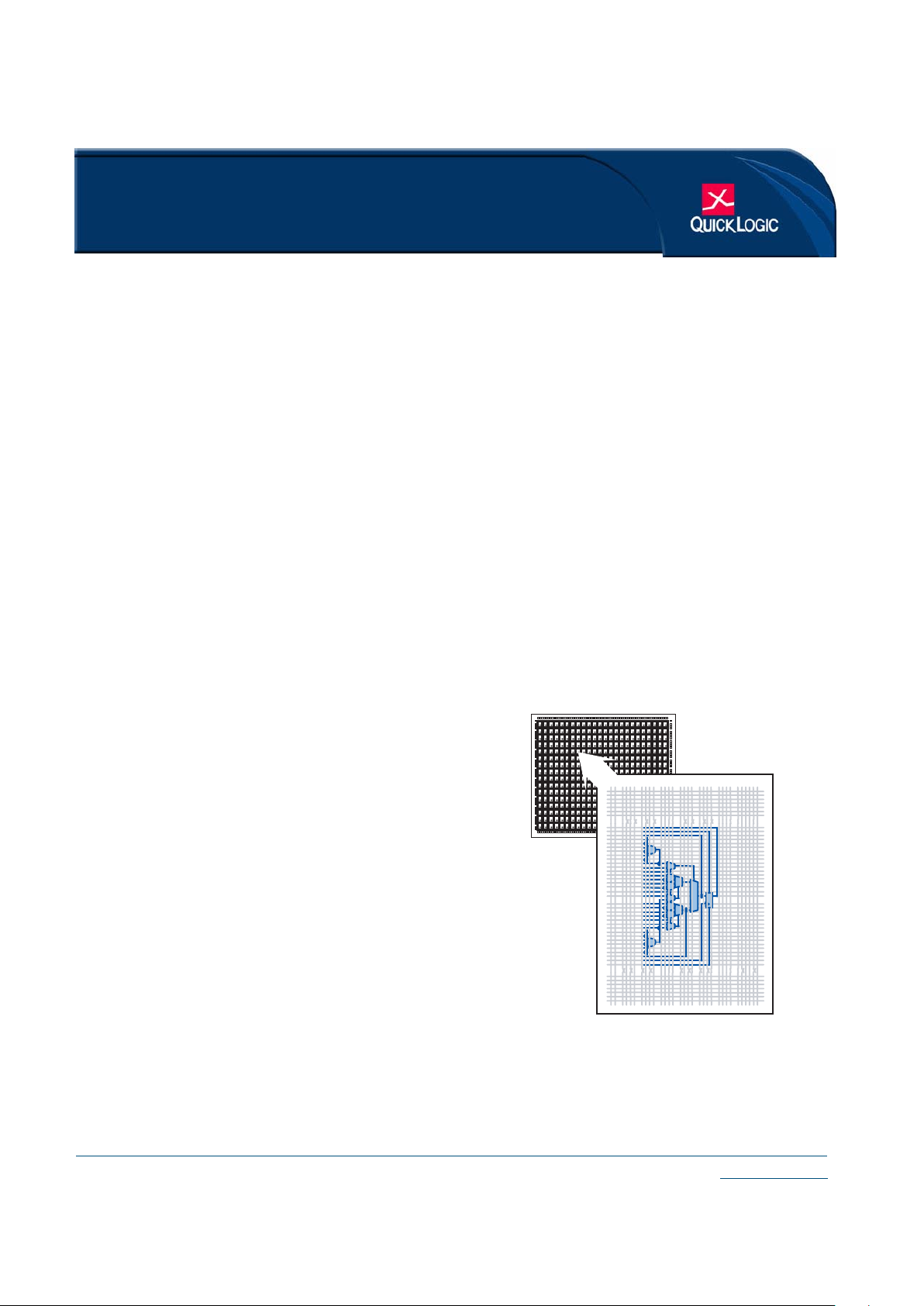
Figure 1: 320 pASIC 3 Logic Cells
QL3012 pASIC 3 FPGA Data Sheet
12,000 Usable PLD Gate pASIC 3 FPGA Combining High Performance
and High Density
Page 2

2
www.quicklogic.com
© 2002 QuickLogic Corporation
•
•
•
•
•
•
QL3012 pASIC 3 FPGA Data Sheet Rev E
Architecture Overview
The QL3012 is a 12,000 usable PLD gate member of the pASIC 3 family of FPGAs. pASIC
3 FPGAs are fabricated on a 0.35 µm four-layer metal process using QuickLogic
's patented
ViaLink
technology to provide a unique combination of high performance, high density,
low cost, and extreme ease-of-use.
The QL3012 contains 320 logic cells. With a maximum of 118 I/Os, the QL3012 is
available in 84-pin PLCC, 100-pin TQFP, and 144-pin TQFP packages.
Software support for the complete pASIC 3 family, including the QL3012, is available
through three basic packages. The turnkey QuickWork s
package provides the most
complete FPGA software solution from design entry to logic synthesis, to place and route,
to simulation. The QuickTools
TM
for Workstations package provides a solution for designers
who use Cadence
, ExemplarTM, Mentor, Synopsys, Synplicity, ViewlogicTM, AldecTM,
or other third-party tools for design entry, synthesis, or simulation.
Page 3
© 2002 QuickLogic Corporation
www.quicklogic.com
3
•
•
•
•
•
•
QL3012 pASIC 3 FPGA Data Sheet Rev E
Electrical Specifications
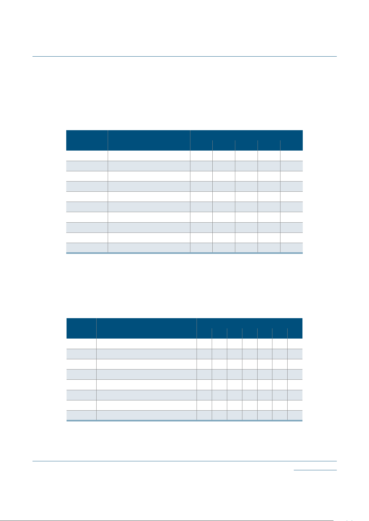
AC Characteristics at VCC = 3.3 V, TA = 25°C (K = 1.00)
To calculate delays, multiply the appropriate K factor from Table 7 by the numbers provided
in
Table 1 through Table 5.
Table 1: Logic Cells
Symbol Parameter Propagation Delays (ns) Fanout
a
a. Stated timing for worst case Propagation Delay over process variation at V
CC
= 3.3 V and
TA = 25°C. Multiply by the appropriate Delay Factor, K, for speed grade, voltage, and temperature
settings as specified in
Table 7.
1 2 3 4 8
t
PD
Combinatorial Delay
b
b. These limits are derived from a representative selection of the slowest paths through the pASIC
3 logic cell including typical net delays. Worst case delay values for sp ecific paths should be determined from timing analysis of your particular design.
1.4 1.7 1.9 2.2 3.2
t
SU
Setup Time
b
1.7 1.7 1.7 1.7 1.7
t
H
Hold Time 0.0 0.0 0.0 0.0 0.0
t
CLK
Clock to Q Delay 0.7 1.0 1.2 1.5 2.5
t
CWHI
Clock High Time 1.2 1.2 1.2 1.2 1.2
t
CWLO
Clock Low Time 1.2 1.2 1.2 1.2 1.2
t
SET
Set Delay 1.0 1.3 1.5 1.8 2.8
t
RESET
Reset Delay 0.8 1.1 1.3 1.6 2.6
t
SW
Set Width 1.9 1.9 1.9 1.9 1.9
t
RW
Reset Width 1.8 1.8 1.8 1.8 1.8
Table 2: Input-Only/Clock Cells
Symbol Parameter Propagation Delays (ns) F a no ut
a
a. Stated timing for worst case Propagation Delay over process variation at V
CC
= 3.3 V and
TA = 25
°C. Multiply by the appropriate Delay Factor, K, for speed grade, voltag e, and tempera-
ture settings as specified in
Table 7.
1 2 3 4 8 12 24
t
IN
High Drive Input Delay 1.5 1.6 1.8 1.9 2.4 2.9 4.4
t
INI
High Drive Input, Inverting Delay 1.6 1.7 1.9 2.0 2.5 3.0 4.5
t
ISU
Input Register Set-Up Time 3.1 3.1 3.1 3.1 3.1 3.1 3.1
t
IH
Input Register Hold Time 0.0 0.0 0.0 0.0 0.0 0.0 0.0
t
lCLK
Input Register Clock To Q 0.7 0.8 1.0 1.1 1.6 2.1 3.6
t
lRST
Input Register Reset Delay 0.6 0.7 0.9 1.0 1.5 2.0 3.5
t
lESU
Input Register clock Enable Set-Up Time 2.3 2.3 2.3 2.3 2.3 2.3 2.3
t
lEH
Input Register Clock Enable Hold Time 0.0 0.0 0.0 0.0 0.0 0.0 0.0
Page 4
4
www.quicklogic.com
© 2002 QuickLogic Corporation
•
•
•
•
•
•
QL3012 pASIC 3 FPGA Data Sheet Rev E
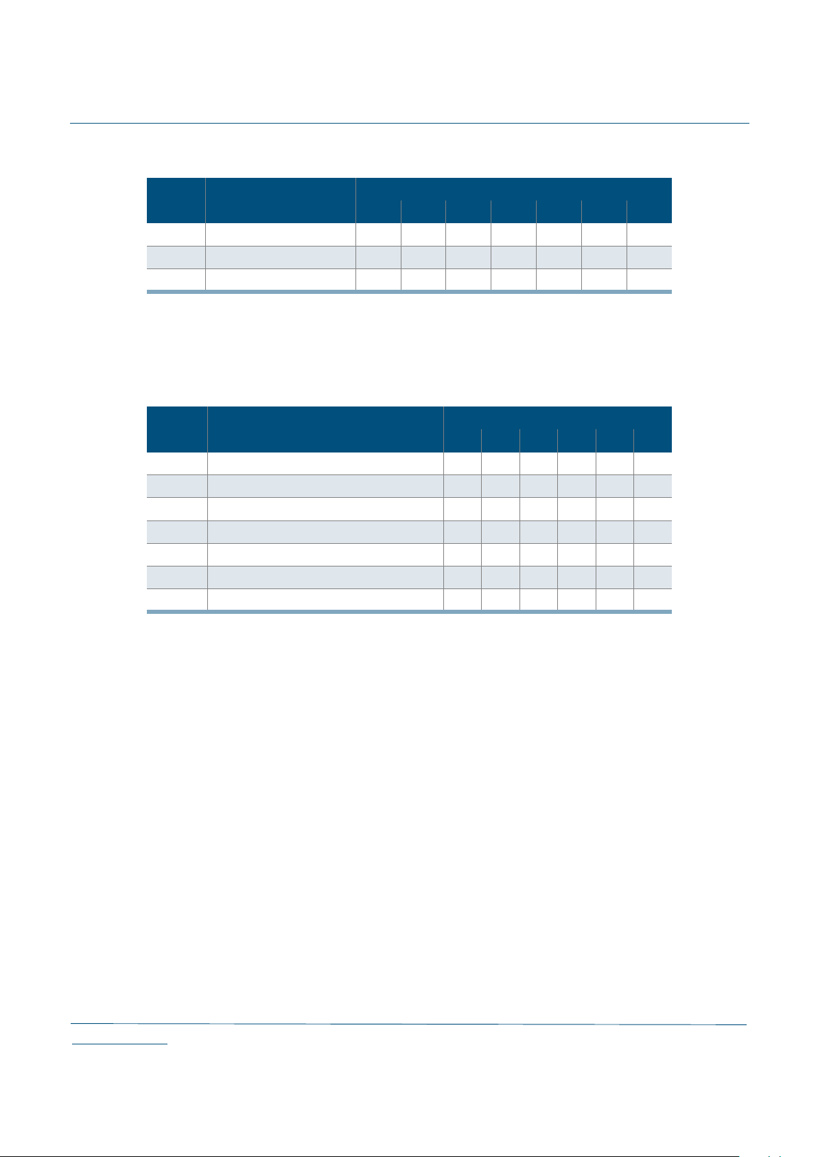
Table 3: Clock Cells
Symbol Parameter Propagation Delays (ns) Loads per Half Column
a
a. The array distributed networks consist of 40 half columns and the global distributed networks con-
sist of 44 half columns, each driven by an independent buffer. The number of half columns used
does not affect clock buffer delay. The array clock has up to eight loads per half column. The global clock has up to 11 loads per half column.
1 2 3 4 8 10 11
t
ACK
Array Clock Delay 1.2 1.2 1.3 1.3 1.5 1.6 1.7
t
GCKP
Global Clock Pin Delay 0.7 0.7 0.7 0.7 0.7 0.7 0.7
t
GCKB
Global Clock Buffer Delay 0.8 0.8 0.9 0.9 1.1 1.2 1.3
Table 4: Input-Only I/O Cells
Symbol Parameter Propagation Delays (ns) Fanout
a
a. Stated timing for worst case Propagation Delay over process variation at V
CC
= 3.3 V and
TA = 25°C. Multiply by the appropriate Delay Factor, K, for speed grade, voltage, and temperature
settings as specified in Table 7.
1 2 3 4 8 10
t
I/O
Input Delay (bidirectional pad) 1.3 1.6 1.8 2.1 3.1 3.6
t
ISU
Input Register Set-Up Time 3.1 3.1 3.1 3.1 3.1 3.1
t
IH
Input Register Hold Time 0.0 0.0 0.0 0.0 0.0 0.0
t
lOCLK
Input Register Clock To Q 0.7 1.0 1.2 1.5 2.5 3.0
t
lORST
Input Register Reset Delay 0.6 0.9 1.1 1.4 2.4 2.9
t
lESU
Input Register clock Enable Set-Up Time 2.3 2.3 2.3 2.3 2.3 2.3
t
lEH
Input Register Clock Enable Hold Time 0.0 0.0 0.0 0.0 0.0 0.0
Page 5
© 2002 QuickLogic Corporation
www.quicklogic.com
5
•
•
•
•
•
•
QL3012 pASIC 3 FPGA Data Sheet Rev E
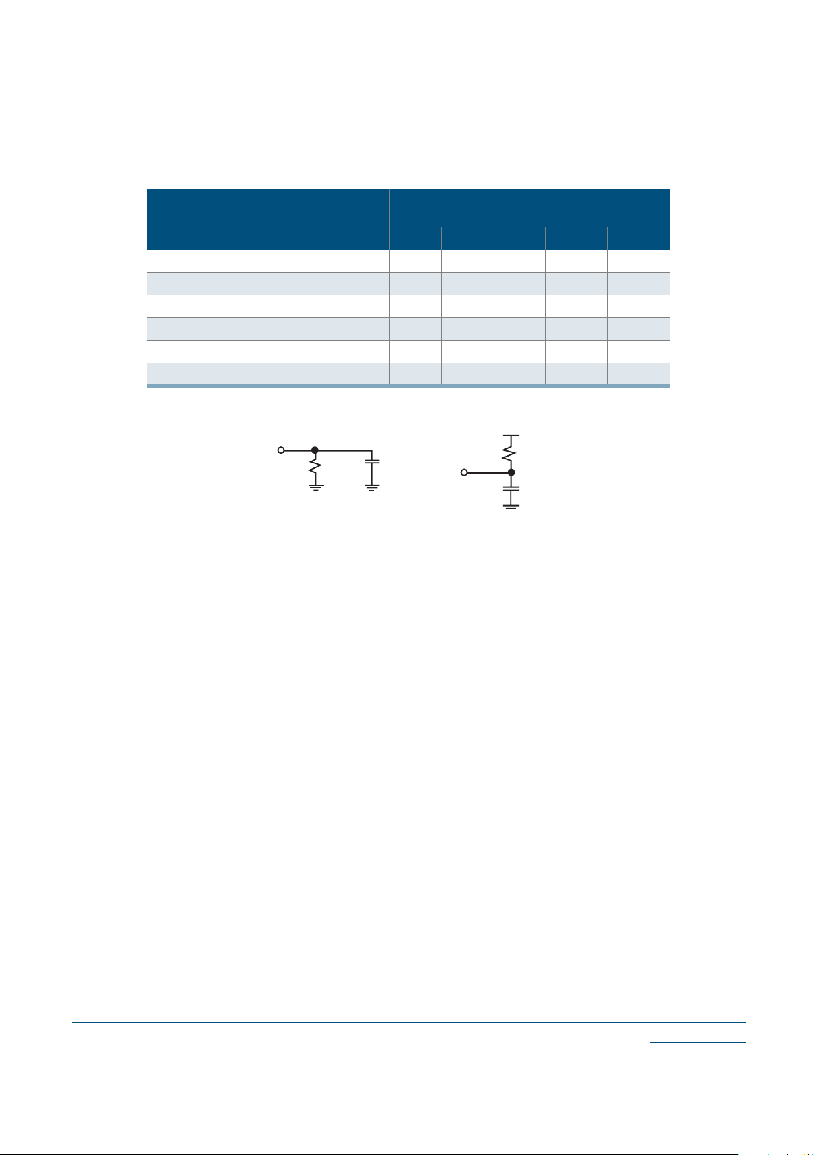
Figure 2: Loads used for t
PXZ
Table 5: Output-Only I/O Cells
Symbol Parameter
Propagation Delays (ns) Output Load
Capacitance (pF)
30 50 75 100 150
t
OUTLH
Output Delay Low to High 2.1 2.5 3.1 3.6 4.7
t
OUTHL
Output Delay High to Low 2.2 2.6 3.2 3.7 4.8
t
PZH
Output Delay Tri-state to High 1.2 1.7 2.2 2.8 3.9
t
PZL
Output Delay Tri-state to Low 1.6 2.0 2.6 3.1 4.2
t
PHZ
Output Delay High to Tri-State
a
a. The loads presented in Figure 2 are used for t
PXZ
:
2.0 - - - -
t
PLZ
Output Delay Low to Tri-State 1.2 - - - -
1ΚΩ
1ΚΩ
t
PHZ
t
PLZ
5 pF
5 pF
Page 6

6
www.quicklogic.com
© 2002 QuickLogic Corporation
•
•
•
•
•
•
QL3012 pASIC 3 FPGA Data Sheet Rev E
DC Characteristics
The DC specifications are provided in Table 6 through Table 8.
Table 6: Absolute Maximum Ratings
Parameter Value Parameter Value
VCC Voltage -0.5 V to 4.6 V DC Input Current ±20 mA
V
CCIO
Voltage -0.5 V to 7.0 V ESD Pad Protection ±2000 V
Input Voltage -0.5 V to V
CCIO
+0.5 V Storage Temperature -65°C to +150°C
Latch-up Immunity ±200 mA Lead Temperature 300°C
Table 7: Operating Range
Symbol Parameter Military Industrial Commercial Unit
Min Max Min Max Min Max
V
CC
Supply Voltage 3.0 3.6 3.0 3.6 3.0 3.6 V
V
CCIO
I/O Input Tolerance Voltage 3.0 5.5 3.0 5.5 3.0 5.25 V
TA Ambient Temperature -55 - -40 85 0 70 °C
TC Case Temperature - 125 - - - - °C
K Delay Factor
-0 Speed Grade - - 0.43 1.90 0.46 1.85 n/a
-1 Speed Grade 0.42 1.64 0.43 1.54 0.46 1.50 n/a
-2 Speed Grade 0.42 1.37 0.43 1.28 0.46 1.25 n/a
-3 Speed Grade 0.43 0.90 0.46 0.88 n/a
-4 Speed Grade 0.43 0.82 0.46 0.80 n/a
Page 7
© 2002 QuickLogic Corporation
www.quicklogic.com
7
•
•
•
•
•
•
QL3012 pASIC 3 FPGA Data Sheet Rev E
Table 8: DC Characteristics
Symbol Parameter Conditions Min Max Units
V
IH
Input HIGH Voltage 0.5 V
CCVCCIO
+0.5 V
V
IL
Input LOW Voltage -0.5 0.3 V
CC
V
V
OH
Output HIGH Voltage
IOH = -12 mA 2.4 V
IOH = -500 µA 0.9 V
CC
V
V
OL
Output LOW Voltage
IOL = 16 mA
a
a. Applies only to -1/-2/-3/-4 commercial grade devices. These speed grades are also PCI-compliant. All
other devices have 8 mA IOL specifications.
0.45 V
IOL = 1.5 mA 0.1 V
CC
V
I
I
I or I/O Input Leakage Current VI = V
CCIO
or GND -10 10 µA
I
OZ
3-State Output Leakage Current VI = V
CCIO
or GND -10 10 µA
C
I
Input Capacitance
b
b. Capacitance is sample tested only. Clock pins are 12 pF maximum.
10 pF
I
OS
Output Short Circuit Current
c
c. Only one output at a time. Duration should not exceed 30 seconds.
VO = GND -15 -180 mA
VO = V
CC
40 210 mA
I
CC
D.C. Supply Current
d
d. For -1/-2/-3/-4 commercial grade devices only. Maximum ICC is 3 mA for -0 commercial grade and all
industrial grade devices, and 5 mA for all military grade devices. For AC conditions, contact QuickLogic customer applications group (see
Contact Information).
VI, VIO = V
CCIO
or GND 0.50 (typ) 2 mA
I
CCIO
D.C. Supply Current on V
CCIO
0 100 µA
Page 8

8
www.quicklogic.com
© 2002 QuickLogic Corporation
•
•
•
•
•
•
QL3012 pASIC 3 FPGA Data Sheet Rev E
Kv and Kt Graphs
Figure 3: Voltage Fa cto r vs. Supply Voltage
Figure 4: Temperature Factor vs. Operating Temperature
0.9200
0.9400
0.9600
0.9800
1.0000
1.0200
1.0400
1.0600
1.0800
1.1000
3 3.1 3 .2 3 .3 3 .4 3.5 3.6
Voltage Factor vs. Supply Voltage
Supply Voltage (V)
Kv
0.85
0.90
0.95
1.00
1.05
1.10
1.15
-60 -40 -20 0 20 40 60 80
Temper ature Factor vs. Ope ra ting Tempe ra tur e
Junction Tem per ature C
Kt
Page 9

© 2002 QuickLogic Corporation
www.quicklogic.com
9
•
•
•
•
•
•
QL3012 pASIC 3 FPGA Data Sheet Rev E
Power-up Sequencing
Figure 5: Power-up Requirements
The following requirements must be met when powering up the device: (Refer to Figure 5)
• When ramping up the power supplies keep (V
CCIO
-VCC)
MAX
≤ 500 mV. Deviation from
this recommendation can cause permanent damage to the device.
• V
CCIO
must lead VCC when ramping the device.
• The power supply must take greater than or equal to 400 µs to reach V
CC
. Ramping to
V
CC/VCCIO
earlier than 400 µs can cause the device to behave improperly.
An internal diode is present in-between VCC and V
CCIO
, as shown in Figure 6.
Figure 6: Internal Diode Between VCC and V
CCIO
Voltage
V
CCIO
V
CC
(V
CCIO
-VCC)
MAX
Time
400 us
V
CC
V
CC
V
CCIO
Internal Logic
Cells, RAM
blocks, etc
IO Cells
Page 10

10
www.quicklogic.com
© 2002 QuickLogic Corporation
•
•
•
•
•
•
QL3012 pASIC 3 FPGA Data Sheet Rev E
JTAG
Figure 7: JTAG Block Diagram
Microprocessors and Application Specific Integrated Circuits (ASICs) pose many design
challenges, not the least of which concerns the accessibility of test points. The Joint Test
Access Group (JTAG) formed in response to this challenge, resulting in IEEE standard
1149.1, the Standard Test Access Port and Boundary Scan Architecture.
The JTAG boundary scan test methodology allows complete observation and control of the
boundary pins of a JTAG-compatible device through JTAG software. A Test Access Port
(TAP) controller works in concert with the Instruction Register (IR); these allow users to run
three required tests, along with several user-defined tests.
JTAG tests allow users to reduce system debug time, reuse test platforms and tools, and reuse
subsystem tests for fuller verification of higher level system elements.
TCK
TMS
TRSTB
RDI
TDO
Instruction Decode
&
Control Logic
TAp Controller
State Machine
(16 States)
Instruction Register
Boundary-Scan Register
(Data Register)
Mux
Bypass
Register
Mux
Internal
Register
I/O Registers
User Defined Data Register
Page 11

© 2002 QuickLogic Corporation
www.quicklogic.com
11
•
•
•
•
•
•
QL3012 pASIC 3 FPGA Data Sheet Rev E
The 1149.1 standard requires the following three tests:
• Extest Instruction. The Extest instruction performs a PCB interconnect test. This test
places a device into an external boundary test mode, selecting the boundary scan
register to be connected between the TAP's Test Data In (TDI) and Test Data Out (TDO)
pins. Boundary scan cells are preloaded with test patterns (via the Sample/Preload
Instruction), and input boundary cells capture the input data for analysis.
• Sample/Preload Instruction. This instruction allows a device to remain in its
functional mode, while selecting the boundary scan register to be connected between
the TDI and TDO pins. For this test, the boundary scan register can be accessed via a
data scan operation, allowing users to sample the functional data entering and leaving
the device.
• Bypass Instruction. The Bypass instruction allows data to skip a device's boundary
scan entirely, so the data passes through the bypass register. The Bypass instruction
allows users to test a device without passing through other devices. The bypass register
is connected between the TDI and TDO pins, allowing serial data to be transferred
through a device without affecting the operation of the device.
Page 12

12
www.quicklogic.com
© 2002 QuickLogic Corporation
•
•
•
•
•
•
QL3012 pASIC 3 FPGA Data Sheet Rev E
Pin Descriptions
Ordering Information
* Contact QuickLogic regarding availability (see Contact Information)
Table 9: Pin Descriptions
Pin Function Description
TDI Test Data In for JTAG
Hold HIGH during normal operation. Connect to
V
CC
if not used for JTAG.
TRSTB Active low Reset for JTAG
Hold LOW during normal operation. Connect to
ground if not used for JTAG.
TMS Test Mode Select for JTAG
Hold HIGH during normal operation. Connect to
V
CC
if not used for JTAG.
TCK Test Clock for JTAG
Hold HIGH or LOW during normal operation.
Connect to VCC or ground if not used for JTAG.
TDO Test data out for JTAG
Output that must be left unconnected if not used for
JTAG.
STM Special Test Mode Must be grounded during normal operation.
I/ACLK
High-drive input and/or array
network driver
Can be configured as either or both.
I/GCLK
High-drive input and/or global
network driver
Can be configured as either or both.
I High-drive input Use for input signals with high fanout.
I/O Input/Output pin Can be configured as an input and/or output.
V
CC
Power supply pin Connect to 3.3 V supply.
V
CCIO
Input voltage tolerance pin
Connect to 5.0 V supply if 5 V input tolerance is
required, otherwise connect to 3.3 V supply.
GND Ground pin Connect to ground.
QL 3012 - 1 PQ208 C
QuickLogic device
pASIC 3 device
part number
Speed Grade
0 = Quick
1 = Fast
2 = Faster
3 = Faster
*4 = Wow
Operating Range
C = Commercial
I = Industrial
M = Military
Package Code
PL84 = 84-pin PLCC
PF100 = 100-pin TQFP
PF144 = 144-pin TQFP
Page 13

© 2002 QuickLogic Corporation
www.quicklogic.com
13
•
•
•
•
•
•
QL3012 pASIC 3 FPGA Data Sheet Rev E
84 PLCC Pinout Diagram
Figure 8: Top View of 84 Pin PLCC
84 PLCC Pinout Diagram
Table 10: 84 PLCC Pinout Diagram
84 PLCC Function 84 PLCC Function 84 PLCC Function 84 PLCC Function
1
I/O
22
ACLK/I
43
I/O
64
ACLK/I
2
I/O
23
I
44
I/O
65
I
3
I/O
24
GCLK/I
45
I/O
66
GCLK/I
4
V
CCIO
25
V
CC
46
V
CCIO
67
V
CC
5
I/O
26
I/O
47
I/O
68
I/O
6
I/O
27
I/O
48
I/O
69
I/O
7
I/O
28
I/O
49
I/O
70
I/O
8
I/O
29
I/O
50
I/O
71
I/O
9
I/O
30
I/O
51
I/O
72
I/O
10
I/O
31
I/O
52
TRSTB
73
I/O
11
TDO
32
I/O
53
TMS
74
I/O
12
I/O
33
TDI
54
I/O
75
TCK
13
I/O
34
I/O
55
I/O
76
STM
14
I/O
35
I/O
56
I/O
77
I/O
15
I/O
36
V
CC
57
I/O
78
I/O
16
I/O
37
I/O
58
I/O
79
V
CC
17
I/O
38
I/O
59
I/O
80
I/O
18
I/O
39
I/O
60
I/O
81
I/O
19
GND
40
GND
61
GND
82
GND
20
I/O
41
I/O
62
I/O
83
I/O
21
I
42
I/O
63
I
84
I/O
TDO
IOIOIOIOIO
IO
VCCIO
IOIOIOIOIO
GND
IO
IO
VCC
IO
IO
STM
TCK
IO
IO
IO
IO
IO
IO
IO
VCC
GCLK/I
I
ACLK/I
I
IO
GND
IO
IO
IO
IO
IO
IO
IO
TDIIOIO
VCCIOIOIOGNDIOIOIOIOIOVCCIOIOIOIOIOIOTRSTB
TMS
74
73
72
71
70
69
68
67
66
65
64
63
62
61
60
59
58
57
56
55
54
33 34 35 36 37 38 39 40 41 42 43 44 45 46 47 48 49 50 51 52 53
12
13
14
15
16
17
18
19
20
21
22
23
24
25
26
27
28
29
30
31
32
QL3012-1PF84C
pASIC 3
IO
IO
IO
IO
IO
IO
IO
GND
IO
I
ACLK/I
I
GCLK/I
VCC
IO
IO
IO
IO
IO
IO
IO
11 10 9 8 7 6 5 4 3 2 1 84 83 82 81 80 79 78 77 76 75
Page 14
14
www.quicklogic.com
© 2002 QuickLogic Corporation
•
•
•
•
•
•
QL3012 pASIC 3 FPGA Data Sheet Rev E
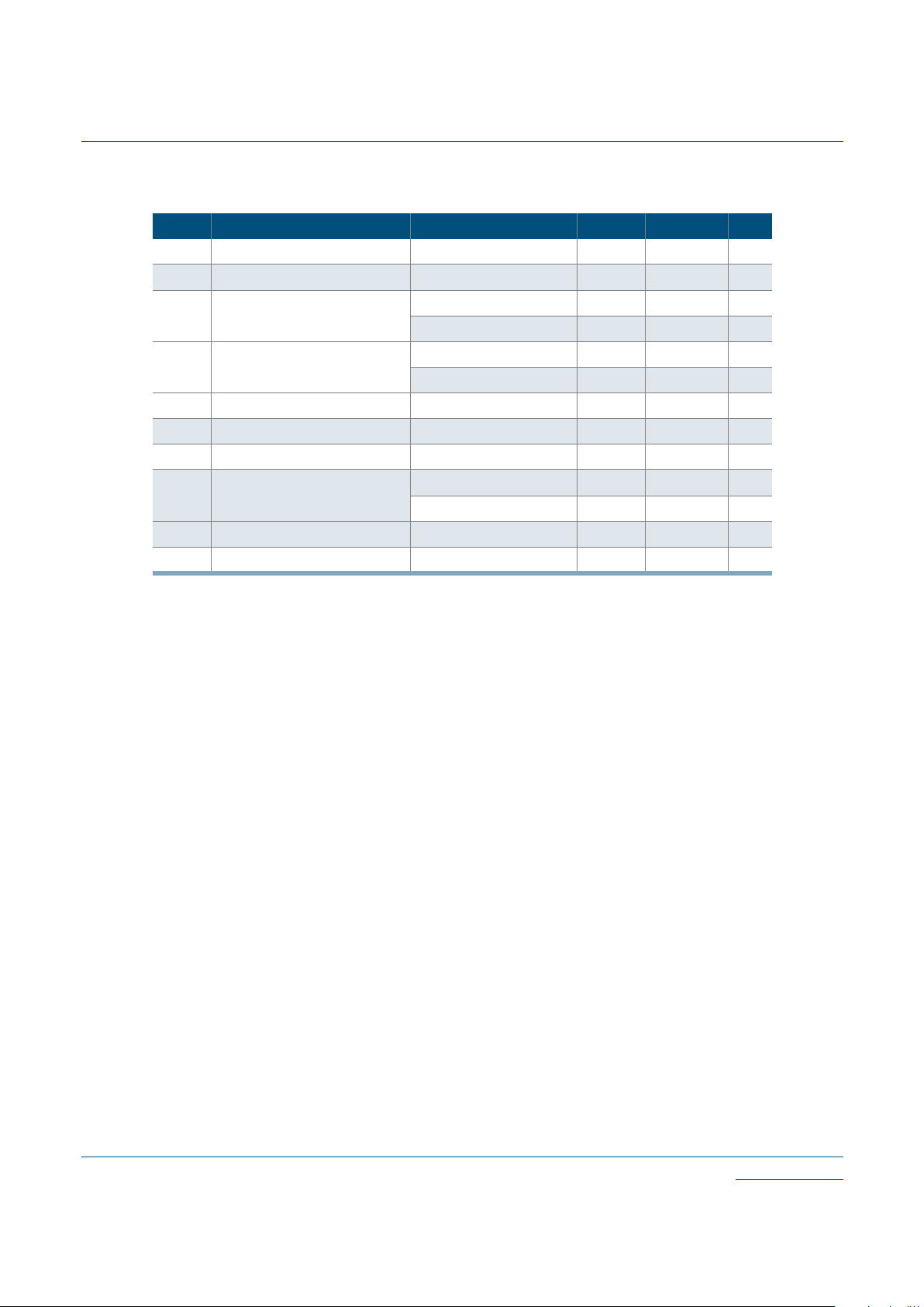
100 TQFP Pinout Diagram
Figure 9: Top View of 100 Pin TQFP
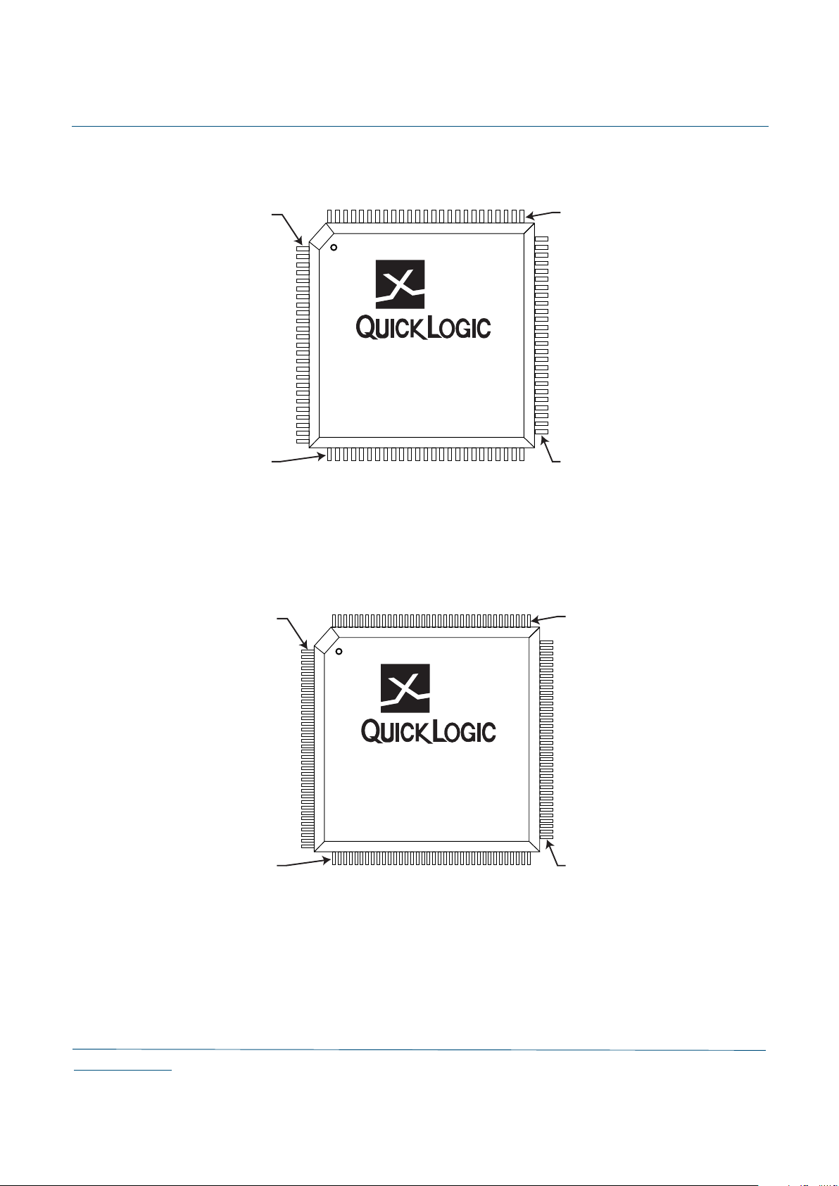
144 TQFP Pinout Diagram
Figure 10: Top View of 144 Pin TQFP
Pin 1
Pin 26 Pin 51
Pin 76
QL3012-1PF100C
pASIC 3
Pin 1
Pin 37 Pin 73
Pin 109
QL3012-1PF144C
pASIC 3
Page 15

© 2002 QuickLogic Corporation
www.quicklogic.com
15
•
•
•
•
•
•
QL3012 pASIC 3 FPGA Data Sheet Rev E
100 & 144 TQFP Pinout Table
Table 11: 100 & 144 TQFP Pinout Table
144
TQFP
100
TQFP
Function
144
TQFP
100
TQFP
Function
144
TQFP
100
TQFP
Function
144
TQFP
100
TQFP
Function
12
I/O
38 26
TDI
75 53
I/O 111 78 I/O
2 3
I/O
39 27
I/O
76 54
I/O
112 79
I/O
3NC
I/O
40 28
I/O
77 55
I/O
113 80
I/O
4 4
I/O
41 29
I/O
78 NC
I/O
114 NC
V
CC
5NC
I/O
42 NC
V
CC
79 NC
V
CC
115 81
I/O
6 5
I/O
43 30
I/O
80 NC
I/O
116 82
I/O
7NC
V
CC
44 31
I/O
81 56
I/O
117 83
I/O
8 6
I/O
45 NC
I/O
82 NC
I/O
118 NC
I/O
9NC
I/O
46 32
I/O
83 57
I/O
119 84
I/O
10 7
I/O
47 33
I/O
84 NC
I/O
120 NC
I/O
11 NC
I/O
48 NC
I/O
85 58
I/O
121 NC
I/O
12 NC
I/O
49 34
I/O
86 NC
I/O
122 85
GND
13 8
I/O
50 35
GND
87 59
GND
123 NC
I/O
14 NC
I/O
51 36
I/O
88 60
I/O
124 86
I/O
15 9
GND
52 NC
I/O
89 61
I
125 87
I/O
16 10
I/O
53 37
I/O
90 62
ACLK / I
126 88
GND
17 11
I
54 38
GND
91 63
V
CC
127 89
I/O
18 12
ACLK / I
55 39
I/O
92 64
I
128 90
I/O
19 13
V
CC
56 40
I/O
93 65
GCLK / I
129 91
I/O
20 14
I
57 41
I/O
94 66
V
CC
130 92
V
CCIO
21 15
GCLK / I
58 42
V
CCIO
95 67
I/O
131 NC
I/O
22 16
V
CC
59 NC
I/O
96 NC
I/O
132 93
I/O
23 17
I/O
60 43
I/O
NC 68
I/O
133 NC
I/O
24 18
I/O
61 44
I/O
97 NC
I/O
134 94
I/O
25 NC
I/O
62 45
I/O
98 69
I/O
135 NC
I/O
26 19
I/O
63 NC
I/O
99 NC
I/O
136 NC
I/O
27 NC
I/O
64 NC
I/O
100 70
I/O
NC 95
I/O
28 20
I/O
65 46
I/O
101 71
I/O
137 NC
I/O
29 21
I/O
66 NC
GND
102 NC
GND
138 NC
GND
30 NC
GND
67 NC
I/O
103 NC
I/O
139 96
I/O
31 NC
I/O
68 NC
I/O
104 72
I/O
140 97
I/O
32 22
I/O
69 47
I/O
105 NC
I/O
141 98
I/O
33 23
I/O
70 48
I/O
106 73
I/O
142 99
I/O
34 NC
I/O
71 49
TRSTB
107 74
I/O
143 100
TDO
35 NC
I/O
72 50
TMS
108 75
I/O
144 1
I/O
36 24
I/O
73 51
I/O
109 76
TCK
37 25
I/O
74 52
I/O
110 77
STM
Page 16

16
www.quicklogic.com
© 2002 QuickLogic Corporation
•
•
•
•
•
•
QL3012 pASIC 3 FPGA Data Sheet Rev E
Contact Information
Telephone: 408 990 4000 (US)
416 497 8884 (Canada)
44 1932 57 9011 (Europe)
49 89 930 86 170 (Germany)
852 8106 9091 (Asia)
81 45 470 5525 (Japan)
E-mail: info@quicklogic.com
Support: support@quicklogic.com
Web site: http://www.quicklogic.com/
Revision History
Copyright Information
Copyright © 2002 QuickLogic Corporation.
All Rights Reserved.
The information contained in this product brief, and the accompanying software programs
are protected by copyright. All rights are reserved by QuickLogic Corporation. QuickLogic
Corporation reserves the right to make periodic modifications of this product without
obligation to notify any person or entity of such revision. Copying, duplicating, selling, or
otherwise distributing any part of this product without the prior written consent of an
authorized representative of QuickLogic is prohibited.
QuickLogic, QuickWorks, pASIC, and ViaLink are registered trademarks of QuickLogic
Corporation.
Verilog is a registered trademark of Cadence Design Systems, Inc.
All trademarks and registered trademarks are the property of their respective owners.
Table 12: Revision History
Revision Date Comments
A not avail. First release.
B not avail.
C not avail
D May 2001 Update of AC/DC Specs and reformat
E June 2002
Added Kfactor, Power-up, JTAG and mechanical
drawing information. Reformatted.
 Loading...