

Datasheet QL2009-0PB256C, QL2009-0PB256I, QL2009-0PF144C, QL2009-0PF144I, QL2009-0PQ208C Datasheet (QUICK LOGIC)
...Page 1
QL2009
3.3V and 5.0V pASIC 2 FPGA
Combining Speed, Density, Low Cost and Flexibility
Rev. C
pASIC 2
HIGHLIGHTS
… 9,000
usable ASIC gates,
225 I/O pins
QL2009
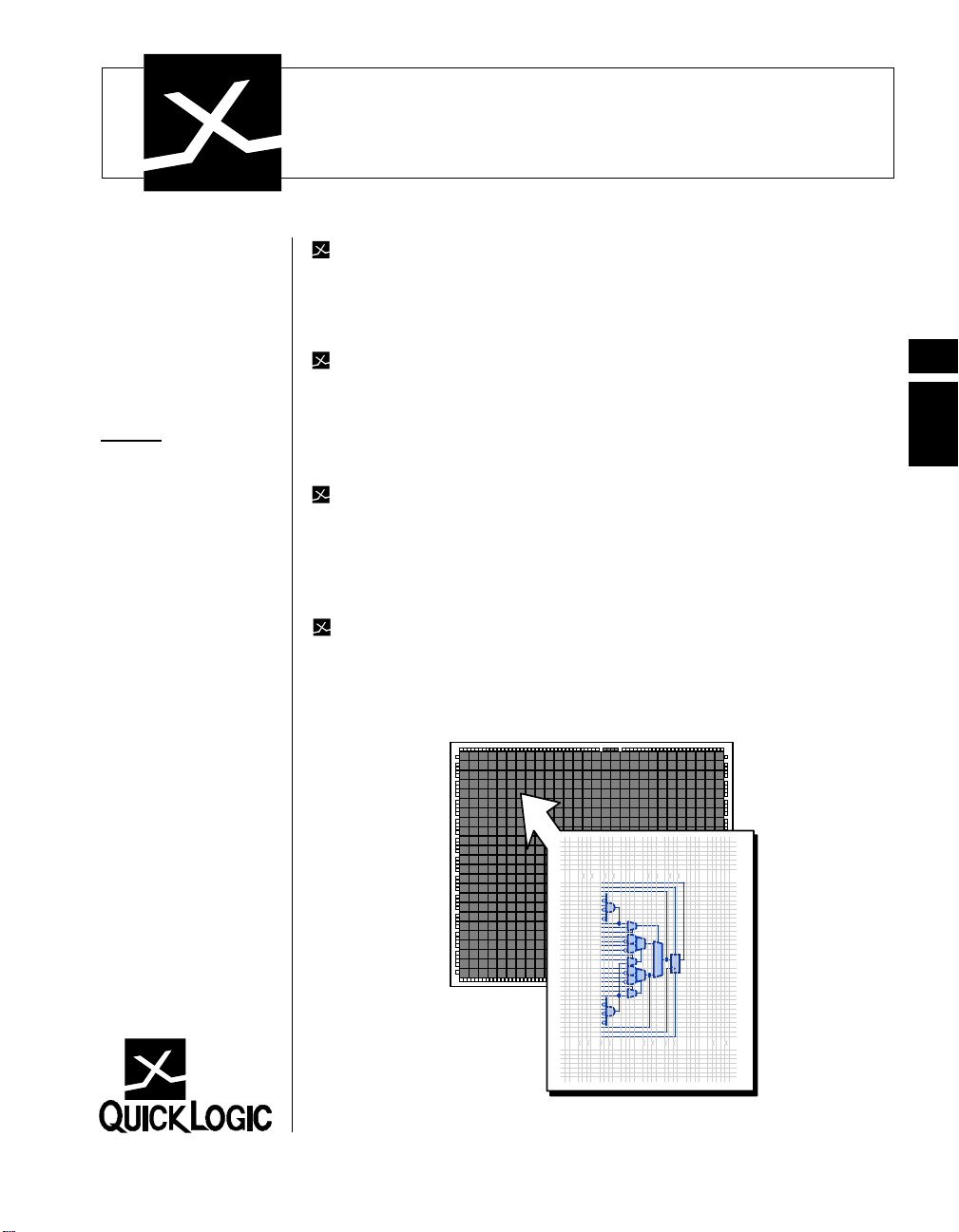
Block Diagram
Ultimate Verilog/VHDL Silicon Solution
-Abundant, high-speed interconnect eliminates manual routing
-Flexible logic cell provides high efficiency and performance
-Design tools produce fast, efficient Verilog/VHDL synthesis
Speed, Density, Low Cost and Flexibility in One Device
-16-bit counter speeds exceeding 200 MHz
-9,000 usable ASIC gates, 16,000 usable PLD gates, 225 I/Os
-3-layer metal ViaLink process for small die sizes
-100% routable and pin-out maintainable
Advanced Logic Cell and I/O Capabilities
-Complex functions (up to 16 inputs) in a single logic cell
-High synthesis gate utilization from logic cell fragments
-Full IEEE Standard JTAG boundary scan capability
-Individually-controlled input/feedback registers and OEs on all I/O pins
Other Important Family Features
-3.3V and 5.0V operation with low standby power
-I/O pin-compatibility between different devices in the same packages
-PCI compliant (at 5.0V), full speed 33 MHz implementations
-High design security provided by security fuses
3
pASIC 2
672
Logic
Cells
3-35
Page 2
QL2009
PRODUCT
SUMMARY
FEATURES
The QL2009 is a 9,000 usable ASIC gate,16,000 usable PLD gate member of
the pASIC 2 family of FPGAs. pASIC 2 FPGAs employ a unique combination
of architecture, technology, and software tools to provide high speed, high
usable density, low price, and flexibility in the same devices. The flexibility
and speed make pASIC 2 devices an efficient and high performance silicon
solution for designs described using HDLs such as Verilog and VHDL, as well
as schematics.
The QL2009 contains 672 logic cells. With 225 maximum I/Os, the QL2009
is available in 144-pin TQFP, 208-PQFP, and 256-pin PBGA packages.
Software support for the complete pASIC families, including the QL2009, is
available through three basic packages. The turnkey QuickWorks package
provides the most complete FPGA software solution from design entry to logic
synthesis (by Synplicity, Inc.), to place and route, to simulation. The
QuickToolsTM and QuickChipTM packages provide a solution for designers
who use Cadence, Mentor, Synopsys, Viewlogic, Veribest, or other third-party
tools for design entry, synthesis, or simulation.
Total of 225 I/O Pins
- 217 bidirectional input/output pins, PCI-compliant at 5.0V
in -1/-2 speed grades
- 4 high-drive input-only pins
- 4 high-drive input/distributed network pins
Four Low-Skew (less than 0.5ns) Distributed Networks
- Two array networks available to logic cell flip-flop clock, set, and
reset - each driven by an input-only pin
- Two global clock/control networks available to F1 logic input, and
logic cell flip-flop clock, set, reset; input and I/O register clock, reset,
enable; and output enable controls - each driven by an input-only pin, or
any input or I/O pin, or any logic cell output or I/O cell feedback
High Performance
- Input + logic cell + output delays under 6 ns
- Datapath speeds exceeding 225 MHz
- Counter speeds over 200 MHz
3-36
Page 3
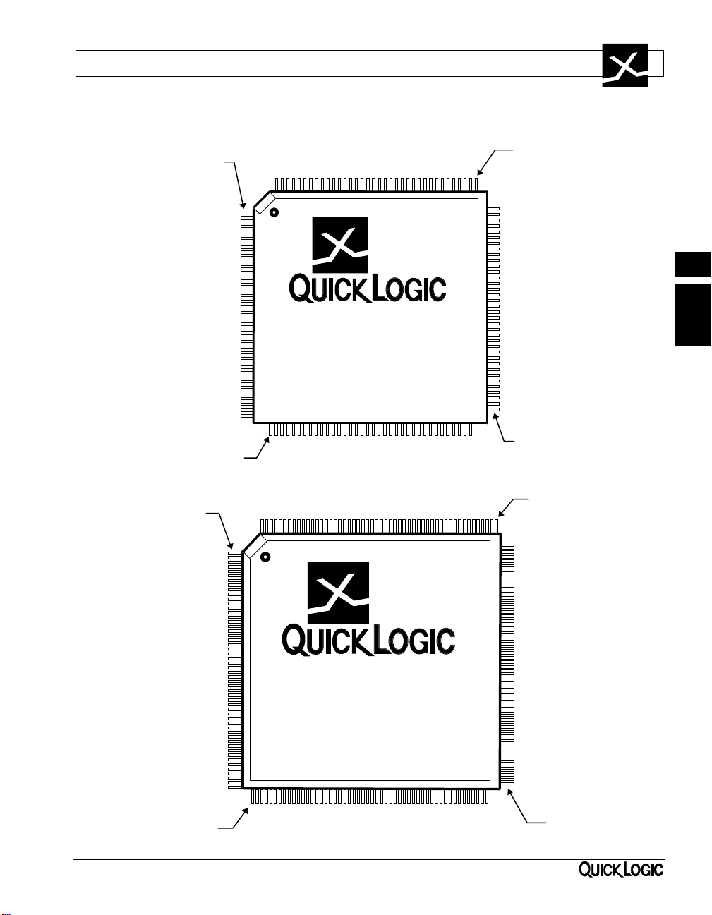
QL2009
PIN # 1
PINOUT DIAGRAMS
PIN # 109
144-PIN TQFP
3
pASIC 2
pASIC
QL2009-1PF144C
PIN # 37
PIN # 1
PIN # 53
208-PIN PQFP
PIN # 73
PIN # 157
pASIC
QL2009-1PQ208C
PIN # 105
3-37
Page 4
QL2009
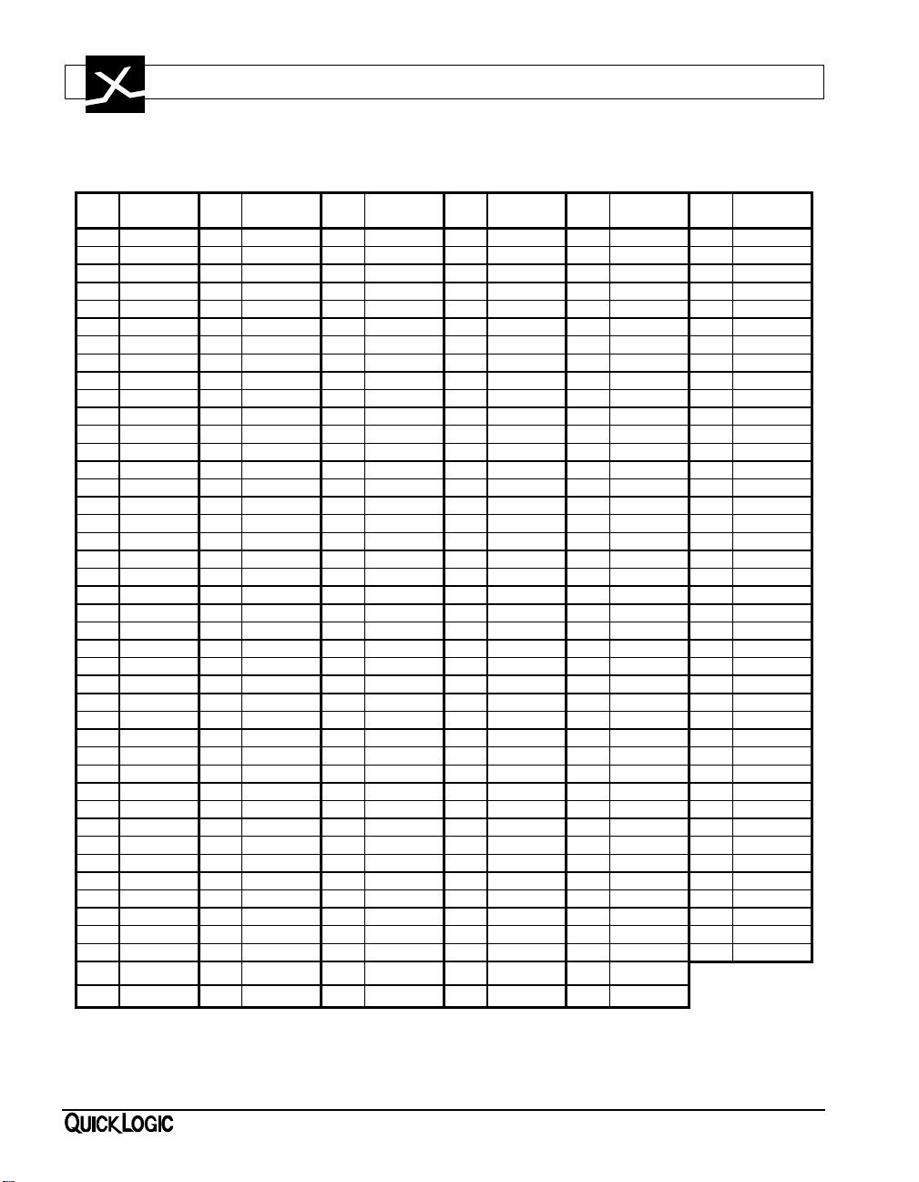
PQFP 208 and TQFP 144 Pinout Table
208 144 Function 208 144 Function 208 144 Function 208 144 Function 208 144 Function
PQFP TQFP PQFP TQFP PQFP TQFP PQFP TQFP PQFP TQFP
1 NC I/O 43 30 GND 85 60 I/O 127 87 GND 169 117 I/O
2 1 I/O 44 31 I/O 86 61 I/O 128 88 I/O 170 118 I/O
3 2 I/O 45 NC I/O 87 NC I/O 129 89 I 171 119 I/O
4 3 I/O 46 32 I/O 88 62 I/O 130 90 ACLK / I 172 120 I/O
5 NC I/O 47 NC I/O 89 63 I/O 131 91 VCC 173 NC I/O
6 4 I/O 48 33 I/O 90 NC I/O 132 92 I 174 NC I/O
7 5 I/O 49 NC I/O 91 NC I/O 133 93 GCLK / I 175 121 I/O
8 NC I/O 50 34 I/O 92 64 I/O 134 94 VCC 176 NC I/O
9 6 I/O 51 35 I/O 93 NC I/O 135 95 I/O 177 122 GND
10 7 VCC 52 36 I/O 94 65 I/O 136 NC I/O 178 123 I/O
11 NC I/O 53 37 I/O 95 66 GND 137 96 I/O 179 124 I/O
12 NC GND 54 38 TDI 96 67 I/O 138 NC I/O 180 NC I/O
13 8 I/O 55 39 I/O 97 NC VCC 139 97 I/O 181 125 I/O
14 NC I/O 56 NC I/O 98 NC I/O 140 98 I/O 182 126 GND
15 9 I/O 57 40 I/O 99 68 I/O 141 NC I/O 183 127 I/O
16 NC I/O 58 NC I/O 100 69 I/O 142 99 I/O 184 128 I/O
17 10 I/O 59 NC GND 101 NC I/O 143 NC I/O 185 129 I/O
18 11 I/O 60 41 I/O 102 70 I/O 144 100 I/O 186 NC I/O
19 12 I/O 61 42 VCC 103 71 TRSTB 145 NC VCC 187 130 VCC
20 13 I/O 62 43 I/O 104 72 TMS 146 101 I/O 188 131 I/O
21 NC I/O 63 NC I/O 105 NC I/O 147 102 GND 189 132 I/O
22 14 I/O 64 44 I/O 106 73 I/O 148 103 I/O 190 NC I/O
23 15 GND 65 45 I/O 107 NC I/O 149 104 I/O 191 133 I/O
24 16 I/O 66 NC I/O 108 74 I/O 150 NC I/O 192 134 I/O
25 17 I 67 46 I/O 109 75 I/O 151 105 I/O 193 NC I/O
26 18 ACLK / I 68 47 I/O 110 76 I/O 152 106 I/O 194 135 I/O
27 19 VCC 69 48 I/O 111 77 I/O 153 NC I/O 195 136 I/O
28 20 I 70 NC I/O 112 NC I/O 154 107 I/O 196 NC I/O
29 21 GCLK / I 71 49 I/O 113 78 I/O 155 NC I/O 197 137 I/O
30 22 VCC 72 NC I/O 114 79 VCC 156 108 I/O 198 NC I/O
31 23 I/O 73 50 GND 115 80 I/O 157 109 TCK 199 138 GND
32 NC I/O 74 51 I/O 116 NC GND 158 110 STM 200 139 I/O
33 24 I/O 75 52 I/O 117 81 I/O 159 111 I/O 201 NC VCC
34 NC I/O 76 NC I/O 118 82 I/O 160 NC I/O 202 140 I/O
35 25 I/O 77 53 I/O 119 NC I/O 161 112 I/O 203 NC I/O
36 NC I/O 78 54 GND 120 83 I/O 162 113 I/O 204 141 I/O
37 26 I/O 79 55 I/O 121 NC I/O 163 NC GND 205 142 I/O
38 27 I/O 80 56 I/O 122 84 I/O 164 NC I/O 206 NC I/O
39 28 I/O 81 NC I/O 123 85 I/O 165 114 VCC 207 143 TDO
40 NC I/O 82 57 I/O 124 NC I/O 166 115 I/O 208 144 I/O
41 NC VCC 83 58 VCC 125 86 I/O 167 116 I/O
42 29 I/O 84 59 I/O 126 NC I/O 168 NC I/O
3-38
Page 5

QL2009
PINOUT DIAGRAM
256-PIN PBGA
pASIC
QL2009-1PB256C
TOP
19 17 15 13 11 9 7 5 3 1
A
B
C
D
E
F
G
H
J
K
L
M
N
P
R
T
U
V
W
Y
3
pASIC 2
PIN A1
CORNER
BOTTOM
3-39
Page 6
QL2009
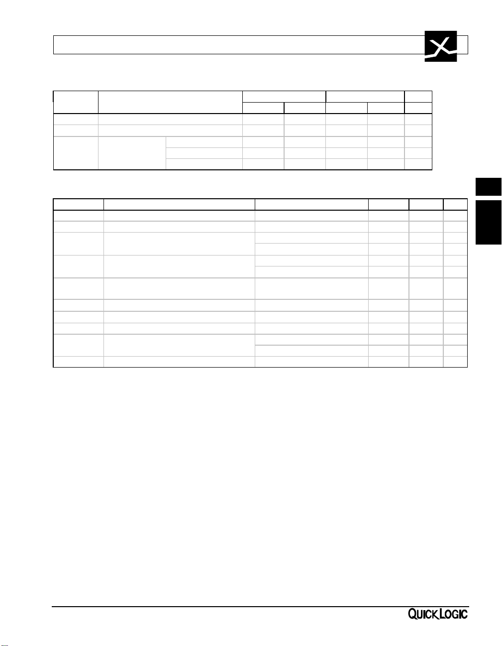
PBGA 256 Pinout Table
256 Function 256 Function 256 Function 256 Function 256 Function 256 Function
PBGA PBGA PBGA PBGA PBGA PBGA
A1 VSS C4 I/O E19 I/O L2 ACLK / I T17 I/O V20 I/O
A2 I/O C5 I/O E20 I/O L3 I T18 I/O W1 I/O
A3 I/O C6 I/O F1 I/O L4 GCLK / I T19 I/O W2 I/O
A4 I/O C7 I/O F2 I/O L17 VCC T20 I/O W3 TDI
A5 I/O C8 I/O F3 I/O L18 I/O U1 I/O W4 I/O
A6 I/O C9 I/O F4 VCC L19 I/O U2 I/O W5 I/O
A7 I/O C10 I/O F17 VCC L20 I/O U3 I/O W6 I/O
A8 I/O C11 I/O F18 I/O M1 I/O U4 VSS W7 I/O
A9 I/O C12 I/O F19 I/O M2 I/O U5 I/O W8 I/O
A10 I/O C13 I/O F20 I/O M3 I/O U6 VCC W9 I/O
A11 I/O C14 I/O G1 I/O M4 I/O U7 I/O W10 I/O
A12 I/O C15 I/O G2 I/O M17 I/O U8 VSS W11 I/O
A13 I/O C16 I/O G3 I/O M18 I/O U9 I/O W12 I/O
A14 I/O C17 I/O G4 I/O M19 I/O U10 VCC W13 I/O
A15 I/O C18 I/O G17 I/O M20 I/O U11 I/O W14 I/O
A16 I/O C19 I/O G18 I/O N1 I/O U12 I/O W15 I/O
A17 I/O C20 I/O G19 I/O N2 I/O U13 VSS W16 I/O
A18 I/O D1 I/O G20 I/O N3 I/O U14 I/O W17 I/O
A19 TCK D2 I/O H1 I/O N4 VSS U15 VCC W18 I/O
A20 I/O D3 I/O H2 I/O N17 VSS U16 I/O W19 I/O
B1 TDO D4 VSS H3 I/O N18 I/O U17 VSS W20 TRSTB
B2 I/O D5 I/O H4 VSS N19 I/O U18 I/O Y1 I/O
B3 I/O D6 VCC H17 VSS N20 I/O U19 I/O Y2 I/O
B4 I/O D7 I/O H18 I/O P1 I/O U20 I/O Y3 I/O
B5 I/O D8 VSS H19 I/O P2 I/O V1 I/O Y4 I/O
B6 I/O D9 I/O H20 I/O P3 I/O V2 I/O Y5 I/O
B7 I/O D10 I/O J1 I/O P4 I/O V3 I/O Y6 I/O
B8 I/O D11 VCC J2 I/O P17 I/O V4 I/O Y7 I/O
B9 I/O D12 I/O J3 I/O P18 I/O V5 I/O Y8 I/O
B10 I/O D13 VSS J4 I/O P19 I/O V6 I/O Y9 I/O
B11 I/O D14 I/O J17 I/O P20 I/O V7 I/O Y10 I/O
B12 I/O D15 VCC J18 I/O R1 I/O V8 I/O Y11 I/O
B13 I/O D16 I/O J19 I/O R2 I/O V9 I/O Y12 I/O
B14 I/O D17 VSS J20 GCLK / I R3 I/O V10 I/O Y13 I/O
B15 I/O D18 I/O K1 I/O R4 VCC V11 I/O Y14 I/O
B16 I/O D19 I/O K2 I/O R17 VCC V12 I/O Y15 I/O
B17 I/O D20 I/O K3 I/O R18 I/O V13 I/O Y16 I/O
B18 STM E1 I/O K4 VCC R19 I/O V14 I/O Y17 I/O
B19 I/O E2 I/O K17 I R20 I/O V15 I/O Y18 I/O
B20 I/O E3 I/O K18 ACLK / I T1 I/O V16 I/O Y19 I/O
C1 I/O E4 I/O K19 I T2 I/O V17 I/O Y20 I/O
C2 I/O E17 I/O K20 I/O T3 I/O V18 I/O
C3 I/O E18 I/O L1 I T4 I/O V19 TMS
3-40
Page 7

QL2009
PIN DESCRIPTIONS
Pin Function Description
TDI Test Data In for JTAG Hold HIGH during normal operation. Connect to
VCC if not used for JTAG.
TRSTB Active low Reset for JTAG Hold LOW during normal operation. Connect to
ground if not used for JTAG.
TMS Test Mode Select for JTAG Hold HIGH during normal operation. Connect to
VCC if not used for JTAG.
TCK Test Clock for JTAG Hold HIGH or LOW during normal operation.
Connect to VCC or ground if not used for JTAG.
TDO Test data out for JTAG Ou t p u t t h a t m u s t b e l e f t u n c onnected if not used for JTAG.
STM Special Test Mode Must be grounded during normal operation.
I/ACLK High-drive input and/or array
network driver
I/GCLK High-drive input and/or global
network driver
I High-drive input Use for input signals with high fanout.
I/O Input/Output pin Can be configured as an input and/or output.
VCC Power supply pin Connect to 3.3V supply.
GND Ground pin Connect to ground.
Can be configured as either or both.
Can be configured as either or both.
3
pASIC 2
QuickLogic
pASIC device
pASIC 2 device
part number
Speed Grade
X = quick
0 = fast
1 = faster
2 = fastest
QL 2009 - 1 PQ208 C
ORDERING
INFORMATION
Operating Range
C = Commercial
I = Industrial
Package Code
PF144 = 144-pin TQFP
PQ208 = 208-pin PQFP
PB256 = 256-pin PBGA
3-41
Page 8

QL2009
ABSOLUTE MAXIMUM RATINGS
Supply Voltage ……………….. -0.5 to 7.0V Storage Temperature……..…….. -65°C to + 150°C
Input Voltage ……….… -0.5 to VCC +0.5V Lead Temperature ………….………………. 300°C
ESD Pad Protection ….…………… ±2000V
DC Input Current ….……………… ±20 mA
Latch-up Immunity ………………. ±200 mA
5 Volt OPERATING RANGE
Symbol Parameter Industrial Commercial Unit
Min Max Min Max
VCC Supply Voltage 4.5 5.5 4.75 5.25 V
TA Ambient Temperature -40 85 0 70
TC Case Temperature
-X Speed Grade 0.4 2.75 0.46 2.55
K Delay Factor -0 Speed Grade 0.4 2.00 0.46 1.85
-1 Speed Grade 0.4 1.61 0.46 1.50
-2 Speed Grade 0.4 1.35 0.46 1.25
DC CHARACTERISTICS over 5V operating range
Symbol Parameter Conditions Min Max Unit
VIH Input HIGH Voltage 2.0 V
VIL Input LOW Voltage 0.8 V
IOH = -4 mA 3.7 V
VOH Output HIGH Voltage IOH = -24 mA/-16 mA [1] 2.4 V
IOH = -10 µA
VOL Output LOW Voltage IOL = 24 mA/16 mA [1] 0.45 V
IOL = 10 µA
II Input Leakage Current VI = VCC or GND -10 10
IOZ 3-State Output Leakage Current VI = VCC or GND -10 10
CI Input Capacitance [2] 10 pF
IOS Output Short Circuit Current [3] VO = GND -15 -120 mA
VO = VCC 40 210 mA
ICC D.C. Supply Current [4] VI, VIO = VCC or GND 2 (typ) 10 mA
VCC-0.1 V
°C
°C
0.1 V
µA
µA
Notes:
[1] -24 mA IOH and 24 mA IOL apply only to -1/-2 commercial grade devices. These speed grades are
also PCI-compliant. All other devices have -16 mA IOH and 16 mA IOL specifications.
[2] Capacitance is sample tested only.
[3] Only one output at a time. Duration should not exceed 30 seconds.
[4] For -0/-1/-2 commercial grade devices only. Maximum ICC is 20 mA for -X commercial grade
devices and 15mA for all industrial grade devices. For AC conditions, contact QuickLogic customer
engineering.
3-42
Page 9
QL2009
3.3 Volt OPERATING RANGE
Symbol Parameter Industrial Commercial Unit
Min Max Min Max
VCC Supply Voltage 3.0 3.6 3.0 3.6 V
TA Ambient Temperature -40 85 0 70
-0 Speed Grade 0.56 2.74 0.61 2.65
K Delay Factor -1 Speed Grade 0.56 2.21 0.61 2.14
-2 Speed Grade 0.56 1.85 0.61 1.79
°C
DC CHARACTERISTICS over 3.3V operating range
Symbol Parameter Conditions Min Max Unit
VIH Input HIGH Voltage 2.0 V
VIL Input LOW Voltage 0.8 V
VOH Output HIGH Voltage IOH = -2.4 mA 2.4 V
IOH = -10 µA
VOL Output LOW Voltage IOL = 4 mA 0.4 V
IOL = 10 µA
IIH Input High Current Sink
(for tolerance to 5V devices)
II Input Leakage Current VI = VCC or GND -10 10
IOZ 3-State Output Leakage Current VI = VCC or GND -10 10
CI Input Capacitance [5] 10 pF
IOS Output Short Circuit Current [6] VO = GND -10 -70 mA
ICC D.C. Supply Current [7] VI, VIO = VCC or GND 0.5 (typ) 3 mA
Notes:
[5] Capacitance is sample tested only.
[6] Only one output at a time. Duration should not exceed 30 seconds.
[7] For commercial grade devices only. Maximum ICC is 5 mA for all industrial grade devices. For AC
conditions, contact QuickLogic customer engineering.
5.5V > VI > VCC 12 mA
VO = VCC 25 130 mA
VCC-0.1 V
0.1 V
3
pASIC 2
µA
µA
3-43
Page 10

QL2009
AC CHARACTERISTICS at VCC = 5V, TA = 25°°C (K = 1.00)
Propagation delays depend on routing, fanout, load capacitance, supply voltage, junction temperature,
and process variation. The AC Characteristics are a design guide to provide initial timing estimates at
nominal conditions. Worst case estimates are obtained when nominal propagation delays are multiplied
by the appropriate Delay Factor, K, as specified in the Delay Factor table (Operating Range). The
QuickChip/QuickTools/QuickWorks software incorporates data sheet AC Characteristics into the
design database for precise path analysis or simulation results following place and route.
Logic Cells
Propagation Delays (ns)
Symbol Parameter
12348
tPD Combinatorial Delay [9] 1.4 1.7 2.0 2.3 3.5
tSU Setup Time [9] 1.8 1.8 1.8 1.8 1.8
tH Hold Time 0.0 0.0 0.0 0.0 0.0
tCLK Clock to Q Delay 0.8 1.1 1.4 1.7 2.9
tCWHI Clock High Time 2.0 2.0 2.0 2.0 2.0
tCWLO Clock Low Time 2.0 2.0 2.0 2.0 2.0
tSET Set Delay 1.4 1.7 2.0 2.3 3.5
tRESET Reset Delay 1.2 1.5 1.8 2.1 3.3
tSW Set Width 1.9 1.9 1.9 1.9 1.9
tRW Reset Width 1.8 1.8 1.8 1.8 1.8
Fanout
[8]
Input-Only Cells
Propagation Delays (ns)
Symbol Parameter
123481224
tIN High Drive Input Delay 2.5 2.6 2.6 2.7 3.5 4.6 5.8
tINI High Drive Input, Inverting Delay 2.6 2.7 2.7 2.8 3.6 4.7 5.9
tISU Input Register Set-Up Time 4.8 4.8 4.8 4.8 4.8 4.8 4.8
tIH Input Register Hold Time 0.0 0.0 0.0 0.0 0.0 0.0 0.0
tlCLK Input Register Clock To Q 0.9 1.0 1.0 1.1 1.9 3.0 4.2
tlRST Input Register Reset Delay 0.8 0.9 0.9 1.0 1.8 2.9 4.1
tlESU Input Register clock Enable Set-Up Time 4.1 4.1 4.1 4.1 4.1 4.1 4.1
tlEH Input Register Clock Enable Hold Time 0.0 0.0 0.0 0.0 0.0 0.0 0.0
Notes:
[8] Stated timing for worst case Propagation Delay over process variation at VCC=5.0V and TA=25°C.
Multiply by the appropriate Delay Factor, K, for speed grade, voltage and temperature settings as
specified in the Operating Range.
[9] These limits are derived from a representative selection of the slowest paths through the pASIC 2 logic
cell including typical net delays. Worst case delay values for specific paths should be determined from
timing analysis of your particular design.
Fanout
[8]
3-44
Page 11

QL2009
Clock Cells
Propagation Delays (ns)
Symbol Parameter
Loads per Half Column
123481013
tACK Array Clock Delay 2.2 2.2 2.3 2.4 2.5 2.6
tGCKP Global Clock Pin Delay 1.2 1.2 1.2 1.2 1.2 1.2 1.2
tGCKB Global Clock Buffer Delay 1.5 1.6 1.6 1.7 1.8 1.9 2.0
[10]
I/O Cells
Propagation Delays (ns)
Symbol Parameter
Fanout
1234810
tI/O Input Delay (bidirectional pad) 1.8 2.1 2.4 2.7 3.9 4.6
tISU Input Register Set-Up Time 4.8 4.8 4.8 4.8 4.8 4.8
tIH Input Register Hold Time 0.0 0.0 0.0 0.0 0.0 0.0
tlOCLK Input Register Clock To Q 0.8 1.1 1.4 1.7 2.9 3.6
tlORST Input Register Reset Delay 0.7 1.0 1.3 1.6 2.8 3.5
tlESU Input Register clock Enable Set-Up Time 4.1 4.1 4.1 4.1 4.1 4.1
tlEH Input Register Clock Enable Hold Time 0.0 0.0 0.0 0.0 0.0 0.0
Propagation Delays (ns)
Symbol Parameter
Output Load Capacitance (pF)
30 50 75 100 150
tOUTLH Output Delay Low to High 2.6 3.0 3.6 4.1 5.2
tOUTHL Output Delay High to Low 2.8 3.3 3.9 4.5 5.7
tPZH Output Delay Tri-state to High 2.1 2.6 3.1 3.7 4.8
tPZL Output Delay Tri-state to Low 2.6 3.3 4.1 4.9 6.5
tPHZ Output Delay High to Tri-State [11] 2.9
tPLZ Output Delay Low to Tri-State [11] 3.3
Notes:
[10] The array distributed networks consist of 48 half columns and the global distributed networks consist of
52 half columns, each driven by an independent buffer. The number of half columns used does not affect
clock buffer delay. The array clock has up to 10 loads per half column. The global clock has up to 13
loads per half column.
[11] The following loads are used for tPXZ:
tPHZ
1K
Ω
5 pF
[8]
1K
Ω
3
pASIC 2
tPLZ
5 pF
3-45
Page 12

QL2009
3-46
 Loading...