

Quectel UG95 Hardware Design

UG95 Hardware Design
UMTS/HSPA Module Series
Rev. UG95_Hardware_Design_V1.3
Date: 2015-03-25
www.quectel.com

UMTS/HSPA Module Series
Quectel
Confidential
UG95 Hardware Design
Our aim is to provide customers with timely and comprehensive service. For any
assistance, please contact our company headquarters:
Quectel Wireless Solutions Co., Ltd.
Office 501, Building 13, No.99, Tianzhou Road, Shanghai, China, 200233
Tel: +86 21 5108 6236
Mail: info@quectel.com
Or our local office, for more information, please visit:
http://www.quectel.com/support/salesupport.aspx
For technical support, to report documentation errors, please visit:
http://www.quectel.com/support/techsupport.aspx
Or Email: Support@quectel.com
GENERAL NOTES
QUECTEL OFFERS THIS INFORMATION AS A SERVICE TO ITS CUSTOMERS. THE INFORMATION
PROVIDED IS BASED UPON CUSTOMERS’ REQUIREMENTS. QUECTEL MAKES EVERY EFFORT
TO ENSURE THE QUALITY OF THE INFORMATION IT MAKES AVAILABLE. QUECTEL DOES NOT
MAKE ANY WARRANTY AS TO THE INFORMATION CONTAINED HEREIN, AND DOES NOT ACCEPT
ANY LIABILITY FOR ANY INJURY, LOSS OR DAMAGE OF ANY KIND INCURRED BY USE OF OR
RELIANCE UPON THE INFORMATION. THE INFORMATION SUPPLIED HEREIN IS SUBJECT TO
CHANGE WITHOUT PRIOR NOTICE.
COPYRIGHT
THIS INFORMATION CONTAINED HERE IS PROPRIETARY TECHNICAL INFORMATION OF
QUECTEL CO., LTD. TRANSMITTABLE, REPRODUCTION, DISSEMINATION AND EDITING OF THIS
DOCUMENT AS WELL AS UTILIZATION OF THIS CONTENTS ARE FORBIDDEN WITHOUT
PERMISSION. OFFENDERS WILL BE HELD LIABLE FOR PAYMENT OF DAMAGES. ALL RIGHTS
ARE RESERVED IN THE EVENT OF A PATENT GRANT OR REGISTRATION OF A UTILITY MODEL
OR DESIGN.
Copyright © Quectel Wireless Solutions Co., Ltd. 2015. All rights reserved.
UG95_Hardware_Design Confidential / Released 1 / 72

UMTS/HSPA Module Series
Revision
Date
Author
Description
1.0
2014-06-20
Yeoman CHEN
Initial
1.1
2014-08-21
Yeoman CHEN
1. Updated transmitting power information.
2. Added reference design for power supply in
Chapter 3.6.3.
3. Updated timing of turning on module in Figure 9.
4. Added definition for the backup capacitor value
in Chapter 3.9.
5. Added reference design of 5V level match circuit
in Figure 18.
6. Updated RS232 level match circuit in Figure 19.
7. Updated frequency range in Table 23.
8. Updated reference circuit of USB interface in
Figure 24.
9. Added diagram for USB upgrade test points.
10. Updated RF output power in Table 28.
11. Updated recommended footprint in Figure 36.
1.2
2014-11-18
Yeoman CHEN
1. Modified VBAT input low voltage to 3.3V.
2. Modified preconditions of entering into the sleep
mode in Chapter 3.5.1.
3. Updated Chapter 3.7.2.
4. Deleted Chapter 3.11.2.
5. Updated antenna requirements in Table 21.
6. Updated recommended footprint in Figure 35.
7. Updated packaging information in Chapter 7.3.
1.3
2015-03-25
Yeoman CHEN/
Jackie WANG
1. Updated Figure 4 & 5.
2. Updated Chapter 3.13.
3. Opened PIN25 CLK_OUT.
4. Added recommended stencil in Chapter 6.2.
Quectel
Confidential
UG95 Hardware Design
About the Document
History
UG95_Hardware_Design Confidential / Released 2 / 72

UMTS/HSPA Module Series
Quectel
Confidential
UG95 Hardware Design
Contents
About the Document ................................................................................................................................... 2
Contents ....................................................................................................................................................... 3
Table Index ................................................................................................................................................... 5
Figure Index ................................................................................................................................................. 6
1 Introduction .......................................................................................................................................... 8
1.1. Safety Information...................................................................................................................... 9
2 Product Concept ................................................................................................................................ 10
2.1. General Description ................................................................................................................. 10
2.2. Key Features ........................................................................................................................... 11
2.3. Functional Diagram ................................................................................................................. 13
2.4. Evaluation Board ..................................................................................................................... 14
3 Application Interface ......................................................................................................................... 15
3.1. General Description ................................................................................................................. 15
3.2. Pin Assignment ........................................................................................................................ 16
3.3. Pin Description ......................................................................................................................... 17
3.4. Operating Modes ..................................................................................................................... 22
3.5. Power Saving ........................................................................................................................... 23
3.5.1. Sleep Mode .................................................................................................................... 23
3.5.1.1. UART Application ................................................................................................. 23
3.5.1.2. USB Application with Suspend Function ............................................................. 24
3.5.1.3. USB Application without Suspend Function ........................................................ 25
3.5.2. Minimum Functionality Mode ......................................................................................... 26
3.6. Power Supply ........................................................................................................................... 26
3.6.1. Power Supply Pins ......................................................................................................... 26
3.6.2. Decrease Voltage Drop .................................................................................................. 27
3.6.3. Reference Design for Power Supply .............................................................................. 28
3.6.4. Monitor the Power Supply .............................................................................................. 29
3.7. Turn on and off Scenarios ....................................................................................................... 29
3.7.1. Turn on Module .............................................................................................................. 29
3.7.2. Turn off Module .............................................................................................................. 31
3.7.2.1. Turn off Module Using AT Command ................................................................... 31
3.7.2.2. Emergency Shutdown .......................................................................................... 32
3.7.2.3. Automatic Shutdown ............................................................................................ 34
3.8. Reset the Module..................................................................................................................... 34
3.9. RTC Interface .......................................................................................................................... 36
3.10. UART Interface ........................................................................................................................ 37
3.11. USIM Card Interface ................................................................................................................ 39
3.12. USB Interface .......................................................................................................................... 42
3.13. PCM and I2C Interface ............................................................................................................ 44
3.14. Network Status Indication ........................................................................................................ 46
UG95_Hardware_Design Confidential / Released 3 / 72

UMTS/HSPA Module Series
Quectel
Confidential
UG95 Hardware Design
3.15. Operating Status Indication ..................................................................................................... 47
4 Antenna Interface ............................................................................................................................... 48
4.1. GSM/UMTS Antenna Interface ................................................................................................ 48
4.1.1. Pin Definition .................................................................................................................. 48
4.1.2. Operating Frequency ..................................................................................................... 48
4.1.3. Reference Design .......................................................................................................... 49
4.2. Antenna Installation ................................................................................................................. 49
4.2.1. Antenna Requirement .................................................................................................... 49
4.2.2. Install the Antenna with RF Connector .......................................................................... 50
5 Electrical, Reliability and Radio Characteristics ............................................................................ 52
5.1. Absolute Maximum Ratings ..................................................................................................... 52
5.2. Power Supply Ratings ............................................................................................................. 52
5.3. Operating Temperature ............................................................................................................ 53
5.4. Current Consumption .............................................................................................................. 53
5.5. RF Output Power ..................................................................................................................... 55
5.6. RF Receiving Sensitivity .......................................................................................................... 56
5.7. Electrostatic Discharge ............................................................................................................ 56
6 Mechanical Dimensions .................................................................................................................... 57
6.1. Mechanical Dimensions of the Module.................................................................................... 57
6.2. Footprint of Recommendation ................................................................................................. 59
6.3. Top View of the Module ........................................................................................................... 61
6.4. Bottom View of the Module ...................................................................................................... 61
7 Storage and Manufacturing .............................................................................................................. 62
7.1. Storage..................................................................................................................................... 62
7.2. Manufacturing and Welding ..................................................................................................... 62
7.3. Packaging ................................................................................................................................ 64
8 Appendix A Reference ....................................................................................................................... 66
9 Appendix B GPRS Coding Scheme ................................................................................................. 70
10 Appendix C GPRS Multi-slot Class .................................................................................................. 71
11 Appendix D EDGE Modulation and Coding Scheme ..................................................................... 72
UG95_Hardware_Design Confidential / Released 4 / 72

UMTS/HSPA Module Series
Quectel
Confidential
UG95 Hardware Design
Table Index
TABLE 1: UG95 SERIES FREQUENCY BANDS .............................................................................................. 10
TABLE 2: UG95 KEY FEATURES ...................................................................................................................... 11
TABLE 3: IO PARAMETERS DEFINITION ........................................................................................................ 17
TABLE 4: PIN DESCRIPTION ........................................................................................................................... 17
TABLE 5: OVERVIEW OF OPERATING MODES ............................................................................................. 22
TABLE 6: VBAT AND GND PINS ....................................................................................................................... 26
TABLE 7: PWRKEY PIN DESCRIPTION .......................................................................................................... 29
TABLE 8: PWRDWN_N PIN DESCRIPTION .................................................................................................... 32
TABLE 9: RESET_N PIN DESCRIPTION ......................................................................................................... 34
TABLE 10: PIN DEFINITION OF THE MAIN UART INTERFACE ..................................................................... 37
TABLE 11: LOGIC LEVELS OF DIGITAL I/O .................................................................................................... 37
TABLE 12: PIN DEFINITION OF THE USIM INTERFACE ............................................................................... 40
TABLE 13: USB PIN DESCRIPTION ................................................................................................................ 42
TABLE 14: PIN DEFINITION OF PCM AND I2C INTERFACE .......................................................................... 44
TABLE 15: PIN DEFINITION OF NETWORK INDICATOR ............................................................................... 46
TABLE 16: WORKING STATE OF THE NETWORK INDICATOR..................................................................... 46
TABLE 17: PIN DEFINITION OF STATUS ........................................................................................................ 47
TABLE 18: PIN DEFINITION OF THE RF ANTENNA ....................................................................................... 48
TABLE 19: THE MODULE OPERATING FREQUENCIES ................................................................................ 48
TABLE 20: ANTENNA CABLE REQUIREMENTS ............................................................................................. 49
TABLE 21: ANTENNA REQUIREMENTS .......................................................................................................... 50
TABLE 22: ABSOLUTE MAXIMUM RATINGS .................................................................................................. 52
TABLE 23: THE MODULE POWER SUPPLY RATINGS .................................................................................. 52
TABLE 24: OPERATING TEMPERATURE ........................................................................................................ 53
TABLE 25: THE MODULE CURRENT CONSUMPTION .................................................................................. 53
TABLE 26: CONDUCTED RF OUTPUT POWER ............................................................................................. 55
TABLE 27: CONDUCTED RF RECEIVING SENSITIVITY ................................................................................ 56
TABLE 28: REEL PACKING .............................................................................................................................. 65
TABLE 29: RELATED DOCUMENTS ................................................................................................................ 66
TABLE 30: TERMS AND ABBREVIATIONS ...................................................................................................... 66
TABLE 31: DESCRIPTION OF DIFFERENT CODING SCHEMES .................................................................. 70
TABLE 32: GPRS MULTI-SLOT CLASSES ...................................................................................................... 71
TABLE 33: EDGE MODULATION AND CODING SCHEME ............................................................................. 72
UG95_Hardware_Design Confidential / Released 5 / 72

UMTS/HSPA Module Series
Quectel
Confidential
UG95 Hardware Design
Figure Index
FIGURE 1: FUNCTIONAL DIAGRAM ............................................................................................................... 14
FIGURE 2: PIN ASSIGNMENT (TOP VIEW) .................................................................................................... 16
FIGURE 3: UART SLEEP APPLICATION ......................................................................................................... 24
FIGURE 4: USB APPLICATION WITH SUSPEND FUNCTION ........................................................................ 25
FIGURE 5: USB SLEEP APPLICATION WITHOUT SUSPEND FUNCTION .................................................... 25
FIGURE 6: VOLTAGE DROP DURING TRANSMITTING BURST .................................................................... 27
FIGURE 7: STAR STRUCTURE OF THE POWER SUPPLY............................................................................ 28
FIGURE 8: REFERENCE CIRCUIT OF POWER SUPPLY .............................................................................. 28
FIGURE 9: TURN ON THE MODULE USING DRIVING CIRCUIT ................................................................... 29
FIGURE 10: TURN ON THE MODULE USING KEYSTROKE ......................................................................... 30
FIGURE 11: TIMING OF TURNING ON MODULE ........................................................................................... 30
FIGURE 12: TIMING OF TURNING OFF THROUGH AT COMMAND ............................................................. 31
FIGURE 13: TURN OFF THE MODULE USING DRIVING CIRCUIT ............................................................... 32
FIGURE 14: TURN OFF THE MODULE USING KEYSTROKE ........................................................................ 33
FIGURE 15: TIMING OF EMERGENCY SHUTDOWN ..................................................................................... 33
FIGURE 16: REFERENCE CIRCUIT OF RESET_N BY USING DRIVING CIRCUIT ...................................... 35
FIGURE 17: REFERENCE CIRCUIT OF RESET_N BY USING BUTTON ...................................................... 35
FIGURE 18: TIMING OF RESETTING MODULE ............................................................................................. 35
FIGURE 19: RTC SUPPLY FROM CAPACITOR .............................................................................................. 36
FIGURE 20: REFERENCE CIRCUIT OF LOGIC LEVEL TRANSLATOR ......................................................... 38
FIGURE 21: REFERENCE CIRCUIT WITH TRANSISTOR CIRCUIT .............................................................. 38
FIGURE 22: RS232 LEVEL MATCH CIRCUIT .................................................................................................. 39
FIGURE 23: REFERENCE CIRCUIT OF THE 8-PIN USIM CARD .................................................................. 40
FIGURE 24: REFERENCE CIRCUIT OF THE 6-PIN USIM CARD .................................................................. 41
FIGURE 25: REFERENCE CIRCUIT OF USB APPLICATION ......................................................................... 42
FIGURE 26: TEST POINTS OF FIRMWARE UPGRADE ................................................................................. 43
FIGURE 27: PCM MASTER MODE TIMING ..................................................................................................... 45
FIGURE 28: REFERENCE CIRCUIT OF PCM APPLICATION WITH AUDIO CODEC .................................... 45
FIGURE 29: REFERENCE CIRCUIT OF THE NETLIGHT ............................................................................... 47
FIGURE 30: REFERENCE CIRCUIT OF THE STATUS ................................................................................... 47
FIGURE 31: REFERENCE CIRCUIT OF ANTENNA INTERFACE ................................................................... 49
FIGURE 32: DIMENSIONS OF THE UF.L-R-SMT CONNECTOR (UNIT: MM) ................................................ 50
FIGURE 33: MECHANICALS OF UF.L-LP CONNECTORS (UNIT: MM) .......................................................... 51
FIGURE 34: SPACE FACTOR OF MATED CONNECTOR (UNIT: MM) ........................................................... 51
FIGURE 35: UG95 TOP AND SIDE DIMENSIONS ........................................................................................... 57
FIGURE 36: UG95 BOTTOM DIMENSION (TOP VIEW) .................................................................................. 58
FIGURE 37: RECOMMENDED FOOTPRINT (TOP VIEW) .............................................................................. 59
FIGURE 38: RECOMMENDED STENCIL OF UG95 (TOP VIEW) ................................................................... 60
FIGURE 39: TOP VIEW OF THE MODULE ...................................................................................................... 61
FIGURE 40: BOTTOM VIEW OF THE MODULE .............................................................................................. 61
FIGURE 41: REFLOW SOLDERING PROFILE ................................................................................................ 63
UG95_Hardware_Design Confidential / Released 6 / 72

UMTS/HSPA Module Series
Quectel
Confidential
UG95 Hardware Design
FIGURE 42: TAPE AND REEL SPECIFICATION .............................................................................................. 64
FIGURE 43: DIMENSIONS OF REEL ............................................................................................................... 65
UG95_Hardware_Design Confidential / Released 7 / 72

UMTS/HSPA Module Series
Quectel
Confidential
UG95 Hardware Design
1 Introduction
This document defines the UG95 module and describes its hardware interface which are connected with
your application and the air interface.
This document can help you quickly understand module interface specifications, electrical and
mechanical details. Associated with application notes and user guide, you can use UG95 module to
design and set up mobile applications easily.
UG95_Hardware_Design Confidential / Released 8 / 72
UMTS/HSPA Module Series
Full attention must be given to driving at all times in order to reduce the risk of an
accident. Using a mobile while driving (even with a handsfree kit) cause distraction
and can lead to an accident. You must comply with laws and regulations restricting
the use of wireless devices while driving.
Switch off the cellular terminal or mobile before boarding an aircraft. Make sure it
switched off. The operation of wireless appliances in an aircraft is forbidden to
prevent interference with communication systems. Consult the airline staff about
the use of wireless devices on boarding the aircraft, if your device offers a Airplane
Mode which must be enabled prior to boarding an aircraft.
Switch off your wireless device when in hospitals or clinics or other health care
facilities. These requests are desinged to prevent possible interference with
sentitive medical equipment.
Cellular terminals or mobiles operate over radio frequency signal and cellular
network and cannot be guaranteed to connect in all conditions, for example no
mobile fee or an invalid SIM card. While you are in this condition and need
emergent help, please remember using emergency call. In order to make or
receive call, the cellular terminal or mobile must be switched on and in a service
area with adequate cellular signal strength.
Your cellular terminal or mobile contains a transmitter and receiver. When it is ON ,
it receives and transmits radio frequency energy. RF interference can occur if it is
used close to TV set, radio, computer or other electric equipment.
In locations with potencially explosive atmospheres, obey all posted signs to turn
off wireless devices such as your phone or other cellular terminals. Areas with
potencially exposive atmospheres including fuelling areas, below decks on boats,
fuel or chemical transfer or storage facilities, areas where the air contains
chemicals or particles such as grain, dust or metal powders.
Quectel
Confidential
UG95 Hardware Design
1.1. Safety Information
The following safety precautions must be observed during all phases of the operation, such as usage,
service or repair of any cellular terminal or mobile incorporating UG95 module. Manufacturers of the cellular
terminal should send the following safety information to users and operating personnel and to incorporate
these guidelines into all manuals supplied with the product. If not so, Quectel does not take on any liability
for customer failure to comply with these precautions.
UG95_Hardware_Design Confidential / Released 9 / 72
UMTS/HSPA Module Series
Module
GSM
850
EGSM
900
DCS
1800
PCS
1900
UMTS
850
UMTS
900
UMTS
1900
UMTS
2100
UG95-A
UG95-E
1)
UG95 series (UG95-A/UG95-E) includes Data-only and Telematics versions. Data-only version does
not support voice function, Telematics version supports it.
NOTE
Quectel
Confidential
UG95 Hardware Design
2 Product Concept
2.1. General Description
UG95 series are embedded 3G wireless communication modules, support GSM/GPRS/EDGE and
UMTS/HSDPA/HSUPA networks. They can also provide voice functionality1) for your specific application.
UG95 offers a maximum data rate of 7.2Mbps on downlink and 5.76Mbps on uplink in HSPA mode.
GPRS supports the coding schemes CS-1, CS-2, CS-3 and CS-4. EDGE supports CS1-4 and MCS1-9
coding schemes. UG95 contains two variants UG95-A and UG95-E. You can choose the dedicated type
based on the wireless network configuration. The following table shows the entire radio band
configuration of UG95 series.
Table 1: UG95 Series Frequency Bands
More details about GPRS/EDGE multi-slot configuration and coding schemes, please refer to Appendix
B, C and D.
With a tiny profile of 23.6mm × 19.9mm × 2.2mm, UG95 can meet almost all requirements for M2M
application such as automotive, metering, tracking system, security solutions, routers, wireless POS, etc..
UG95 is an SMD type module, which can be embedded in application through its 102 LGA pads.
UG95 is integrated with internet service protocols like TCP/UDP and PPP. Extended AT commands have
been developed for you to use these internet service protocols easily.
UG95_Hardware_Design Confidential / Released 10 / 72
UMTS/HSPA Module Series
Feature
Details
Power Supply
Supply voltage: 3.3V ~ 4.3V
Typical supply voltage: 3.8V
Frequency Bands
UG95-A:
UMTS Dual-band: 850/1900MHz
UG95-E:
GSM Dual-band: 900/1800MHz
UMTS Dual-band: 900/2100MHz
Transmission Data
HSDPA category 8: Max 7.2Mbps
HSUPA category 6: Max 5.76Mbps
UMTS: Max 384kbps (DL)/Max 384kbps (UL)
EDGE: Max 236.8kbps (DL only)
GPRS: Max 85.6kbps (DL)/Max 85.6kbps (UL)
CSD: 14.4kbps
Transmitting Power
Class 4 (33dBm±2dB) for EGSM900
Class 1 (30dBm±2dB) for DCS1800
Class 3 (24dBm+1.7/-3.7dB) for UMTS 850/900/1900/2100
HSPA/UMTS Features
Compliant with 3GPP Release 7
WCDMA data rate is corresponded with 3GPP R4
384kbps on downlink and 384kbps on uplink
Support both QPSK and 16-QAM modulations
GSM/GPRS/EDGE
Data Features
GPRS:
Support GPRS multi-slot class 12
Coding scheme: CS-1, CS-2, CS-3 and CS-4
Maximum of four Rx time slots per frame
EDGE:
Support EDGE multi-slot class 12
Support GMSK and 8-PSK for different MCS (Modulation and Coding
scheme)
Coding scheme: MCS 1-9
Downlink only
CSD:
CSD transmission rates: 14.4kbps non-transparent
Support Unstructured Supplementary Services Data (USSD)
Internet Protocol Features
Support TCP/UDP/PPP protocols
Quectel
Confidential
UG95 Hardware Design
2.2. Key Features
The following table describes the detailed features of UG95 module.
Table 2: UG95 Key Features
UG95_Hardware_Design Confidential / Released 11 / 72

UMTS/HSPA Module Series
Support the protocols PAP (Password Authentication Protocol) and
CHAP (Challenge Handshake Authentication Protocol) usually used
for PPP connections
SMS
Text and PDU mode
Point to point MO and MT
SMS cell broadcast
SMS storage: SIM card by default
USIM Interface
Support USIM card: 1.8V, 3.0V
Support USIM and SIM
PCM Interface
Used for audio function with external codec
Supports 8, 16, 32 bit mode with short frame synchronization
Support master mode
UART Interface
Support one UART interface.
7-wire on UART interface, without DSR
Support RTS and CTS hardware flow control
Baud rate 300 to 921600bps
Default autobauding 4800 to 115200bps
Used for AT command, data transmission or firmware upgrade
Multiplexing function
USB Interface
Compliant with USB 1.1/2.0 specification (slave only), the data transfer
rate can reach up to 480Mbps
Used for AT command communication, data transmission, software
debug and firmware upgrade
USB Driver: Support Windows XP, Windows Vista, Windows 7,
Windows 8, Windows CE5.0/6.0*, Linux, Android
AT Commands
Compliant with 3GPP TS 27.007, 27.005 and Quectel enhanced AT
commands
Real Time Clock
Implemented
Network Indication
One pin NETLIGHT to indicate network connectivity status
Antenna Interface
GSM/UMTS antenna, 50Ω
Physical Characteristics
Size: 19.9±0.15 × 23.6±0.15 × 2.2±0.2mm
Interface: LGA
Weight: 2.5g
Temperature Range
Normal operation: -35°C ~ +80°C
Restricted operation: -40°C ~ -35°C and +80°C ~ +85°C 1)
Storage temperature: -45°C ~ +90°C
Firmware Upgrade
USB interface or UART interface
RoHS
All hardware components are fully compliant with EU RoHS directive
Quectel
Confidential
UG95 Hardware Design
UG95_Hardware_Design Confidential / Released 12 / 72

UMTS/HSPA Module Series
1.
1)
means when the module works within this temperature range, RF performance might degrade. For
example, the frequency error or the phase error would increase.
2. *means this feature is under development.
NOTES
Quectel
Confidential
UG95 Hardware Design
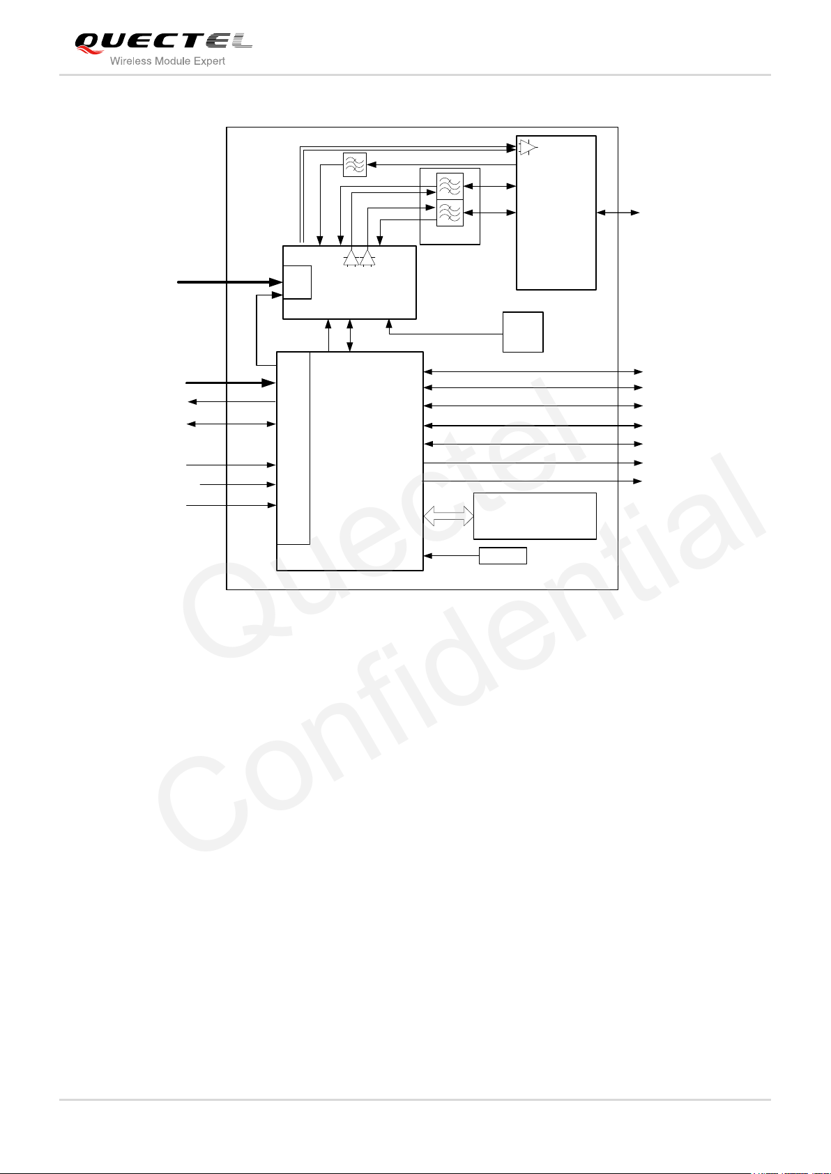
2.3. Functional Diagram
The following figure shows a block diagram of UG95 and illustrates the major functional parts.
RF transceiver
Baseband
DDR+NAND flash
Radio frequency
Peripheral interfaces
--UART interface
--USIM card interface
--USB interface
--PCM interface
--I2C interface
--Status indication
--Control interface
UG95_Hardware_Design Confidential / Released 13 / 72
UMTS/HSPA Module Series
PWRKEY
RESET_N
32kHz
PMU
Baseband
FEM
MCP
RF_ANT
USIM
STATUS
UART
VBAT_BB
USB
VBAT_RF
GSM TX H
UMTS
VDD_EXT
VRTC
Nand+DDR
PWRDWN_N
RF
Transceiver
NETLIGHT
26MHz
DCXO
GSM RX H
UMTS
GSM RX L
3G TX HB
3G TX LB
3G RX HB
3G RX LB
Isoplexer
PCM
GSM TX L
PMU
Reset
I2C
Quectel
Confidential
UG95 Hardware Design
2.4. Evaluation Board
In order to help you to develop applications with UG95, Quectel supplies an evaluation board
(UMTS<E-EVB), RS-232 to USB cable, USB data cable, power adapter, earphone, antenna and other
peripherals to control or test the module. For details, please refer to document [2].
UG95_Hardware_Design Confidential / Released 14 / 72
Figure 1: Functional Diagram

UMTS/HSPA Module Series
Quectel
Confidential
UG95 Hardware Design
3 Application Interface
3.1. General Description
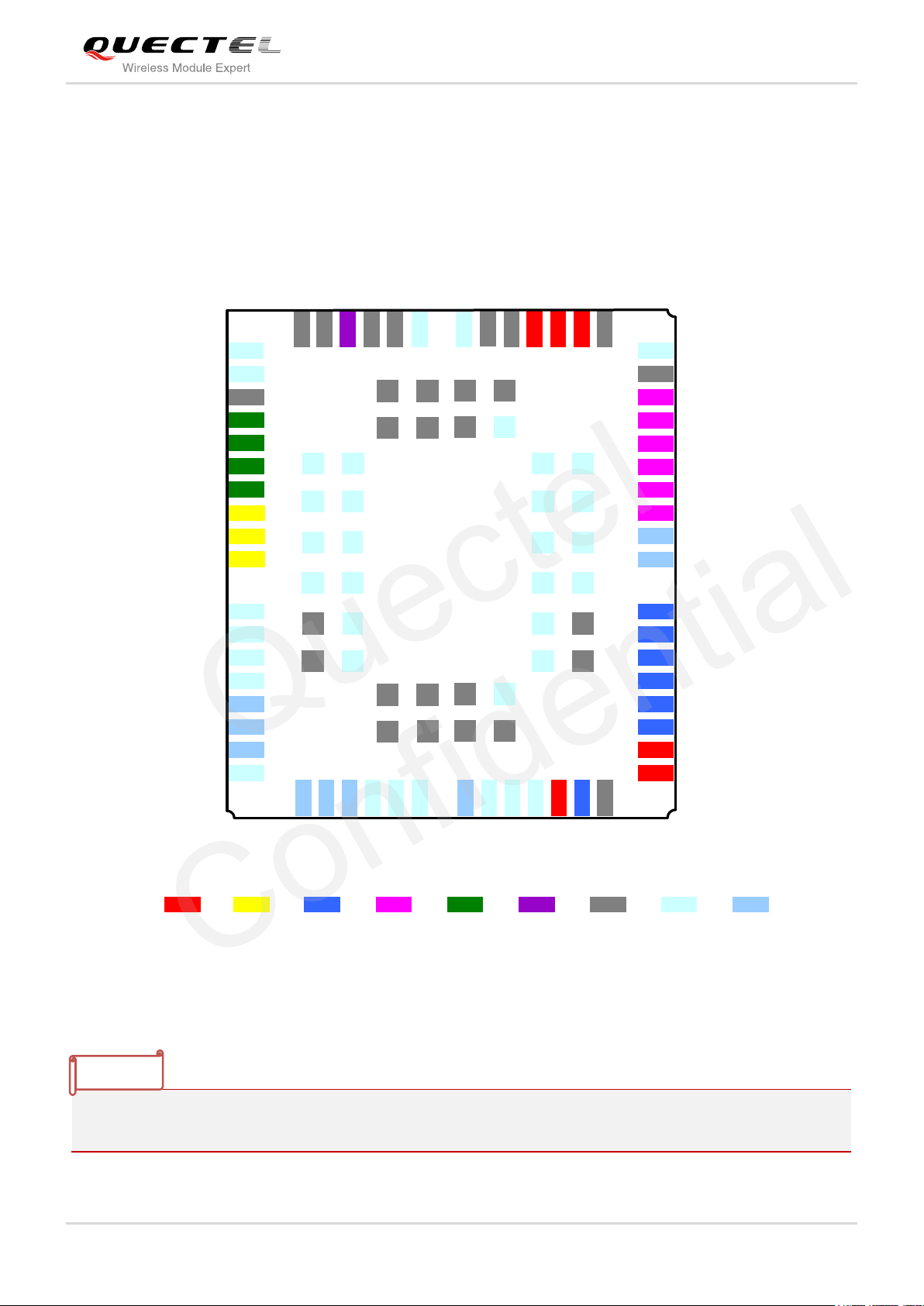
UG95 is equipped with a 62-pin 1.1mm pitch SMT pads plus 40-pin ground pads and reserved pads that
connect to customer’s cellular application platform. Sub-interfaces included in these pads are described in
detail in the following chapters:
Power supply
RTC interface
UART interface
USIM interface
USB interface
PCM interface
Status indication
UG95_Hardware_Design Confidential / Released 15 / 72
UMTS/HSPA Module Series
RESERVED
PCM_SYNC
PCM_CLK
PCM_DIN
PCM_DOUT
RESERVED
RESERVED
PWRKEY
PWRDWN_N
RESET_N
RESERVED
1
2
3
4
5
6
7
11
12
13
14
15
16
17
18
50
51
52
53
54
55
58
59
60
61
62
USB_DM
AP_READY
STATUS
NETLIGHT
RESERVED
RESERVED
RESERVED
CLK_OUT
RESERVED
RESERVED
RESERVED
VDD_EXT
DTR
GND
USIM_CLK
USIM_DATA
USIM_RST
USIM_VDD
RI
DCD
CTS
TXD
RXD
VBAT_BB
VBAT_BB
USIM_GND
GND
RESERVED
31
30
29
28
27
26
23
22
21
20
19
10
9
USB_DP
USB_VBUS
RESERVED
GND
RESERVED
RESERVED
RTS
I2C_SCL
I2C_SDA
8
49
48
47
46
45
44
43
40
41
42
39
38
37
36
35
34
33
32
24
25
57
56
GND
GND
RF_ANT
GND
GND
RESERVED
VBAT_RF
VBAT_RF
GND
GND
RESERVED
VRTC
GND
USIM_PRESENCE
63
64
65
66
67
68
83
84
85
86
87
88
98
97
96
95
94
93
78
77
76
75
74
73
91 92
89 90
71
72
69 70
80 79
82 81
100
99
102 101
POWER USB UART
USIM
OTHERSGND
RESERVED
PCM
ANT
1. Keep all RESERVED pins and unused pins unconnected.
2. GND pads should be connected to ground in the design.
NOTES
Quectel
Confidential
UG95 Hardware Design
3.2. Pin Assignment
The following figure shows the pin assignment of the UG95 module.
Figure 2: Pin Assignment (Top View)
UG95_Hardware_Design Confidential / Released 16 / 72
UMTS/HSPA Module Series
Type
Description
IO
Bidirectional input/output
DI
Digital input
DO
Digital output
PI
Power input
PO
Power output
AI
Analog input
AO
Analog output
OD
Open drain
Power Supply
Pin Name
Pin No.
I/O
Description
DC Characteristics
Comment
VBAT_BB
32, 33
PI
Power supply for
module baseband
part.
Vmax=4.3V
Vmin=3.3V
Vnorm=3.8V
It must be able to
provide sufficient
current in a transmitting
burst which typically
rises to 2.0A.
VBAT_RF
52, 53
PI
Power supply for
module RF part.
Vmax=4.3V
Vmin=3.3V
Vnorm=3.8V
VRTC
51
PI/
PO
Power supply for
internal RTC circuit.
Vnorm=1.8V when
VBAT ≥ 3.3V.
VI=1V~1.9V at
IIN max=2uA when
VBAT is not applied.
If unused, keep this pin
open.
VDD_EXT
29
PO
Provide 1.8V for
external circuit.
Vnorm=1.8V
IOmax=20mA
Power supply for
external GPIO’s pull up
circuits.
Quectel
Confidential
UG95 Hardware Design
3.3. Pin Description
The following tables show the UG95’s pin definition.
Table 3: IO Parameters Definition
Table 4: Pin Description
UG95_Hardware_Design Confidential / Released 17 / 72
UMTS/HSPA Module Series
If unused, keep this pin
open.
GND
3, 31, 48,
50, 54, 55,
58, 59, 61,
62, 67~74,
79~82,
89~91,
100~102
Ground
Turn On/Off
Pin Name
Pin No.
I/O
Description
DC Characteristics
Comment
PWRKEY
15
DI
Turn on the module
RPU≈200kΩ
VIHmax=2.1V
VIHmin=1.3V
VILmax=0.5V
Pull-up to VRTC
internally.
Active low.
PWRDWN_N
16
DI
Turn off the module
RPU≈4.7kΩ
VIHmax=2.1V
VIHmin=1.3V
VILmax=0.5V
Pull-up to VRTC
internally.
Active low.
If unused, keep this
pin open.
RESET_N
17
DI
Reset the module
RPU≈200kΩ
VIHmax=2.1V
VIHmin=1.3V
VILmax=0.5V
Pull-up to VRTC
internally.
Active low.
If unused, keep this
pin open.
Status Indication
Pin Name
Pin No.
I/O
Description
DC Characteristics
Comment
STATUS
20
DO
Indicate the module
operating status.
VOHmin=1.3V
VOLmax=0.5V
1.8V power domain.
If unused, keep this
pin open.
NETLIGHT
21
DO
Indicate the module
network status.
VOHmin=1.3V
VOLmax=0.5V
1.8V power domain.
If unused, keep this
pin open.
USB Interface
Pin Name
Pin No.
I/O
Description
DC Characteristics
Comment
USB_VBUS
8
PI
USB insert
detection.
Vmax=5.25V
Vmin=2.5V
Vnorm=5.0V
USB insert detection.
Quectel
Confidential
UG95 Hardware Design
UG95_Hardware_Design Confidential / Released 18 / 72

UMTS/HSPA Module Series
USB_DP
9
IO
USB differential data
bus.
Compliant with USB
2.0 standard
specification.
Require differential
impedance of 90Ω.
USB_DM
10
IO
USB differential data
bus.
Compliant with USB
2.0 standard
specification.
Require differential
impedance of 90Ω.
USIM Interface
Pin Name
Pin No.
I/O
Description
DC Characteristics
Comment
USIM_GND
47
Specified ground for
USIM card.
USIM_VDD
43
PO
Power supply for
USIM card.
For 1.8V USIM:
Vmax=1.85V
Vmin=1.75V
For 3.0V USIM:
Vmax=2.9V
Vmin=2.8V
Either 1.8V or 3.0V is
supported by the
module automatically.
USIM_DATA
45
IO
Data signal of USIM
card.
For 1.8V USIM:
VILmax=0.35V
VIHmin=1.25V
VOLmax=0.25V
VOHmin=1.25V
For 3.0V USIM:
VILmax=0.5V
VIHmin=2.05V
VOLmax=0.25V
VOHmin=2.05V
Pull-up to USIM_VDD
with 4.7K resistor
internally.
USIM_CLK
46
DO
Clock signal of USIM
card.
For 1.8V USIM:
VOLmax=0.25V
VOHmin=1.25V
For 3.0V USIM:
VOLmax=0.25V
VOHmin=2.05V
USIM_RST
44
DO
Reset signal of
USIM card.
For 1.8V USIM:
VOLmax=0.25V
VOHmin=1.25V
For 3.0V USIM:
VOLmax=0.3V
VOHmin=2.05V
Quectel
Confidential
UG95 Hardware Design
UG95_Hardware_Design Confidential / Released 19 / 72
UMTS/HSPA Module Series
USIM_PRES
ENCE
42
DI
USIM card input
detection.
VILmax=0.35V
VIHmin=1.3V
VIHmax=1.85V
1.8V power domain.
External pull-up
resistor is required.
Main UART Interface
Pin Name
Pin No.
I/O
Description
DC Characteristics
Comment
RI
39
DO
Ring indicator
VOLmax=0.25V
VOHmin=1.55V
1.8V power domain.
If unused, keep this
pin open.
DCD
38
DO
Data carrier
detection
VOLmax=0.25V
VOHmin=1.55V
1.8V power domain.
If unused, keep this
pin open.
CTS
36
DO
Clear to send
VOLmax=0.25V
VOHmin=1.55V
1.8V power domain.
If unused, keep this
pin open.
RTS
37
DI
Request to send
VILmax=0.35V
VIHmin=1.3V
VIHmax=1.85V
1.8V power domain.
If unused, keep this
pin open.
DTR
30
DI
Data terminal ready
VILmax=0.35V
VIHmin=1.3V
VIHmax=1.85V
1.8V power domain.
If unused, keep this
pin open.
TXD
35
DO
Transmit data
VOLmax=0.25V
VOHmin=1.55V
1.8V power domain.
If unused, keep this
pin open.
RXD
34
DI
Receive data
VILmax=0.35V
VIHmin=1.3V
VIHmax=1.85V
1.8V power domain.
If unused, keep this
pin open.
RF Interface
Pin Name
Pin No.
I/O
Description
DC Characteristics
Comment
RF_ANT
60
IO
RF antenna
50Ω impedance
PCM Interface
Pin Name
Pin No.
I/O
Description
DC Characteristics
Comment
PCM_IN
6
DI
PCM data input
VILmin=-0.3V
VILmax=0.35V
VIHmin=1.3V
VIHmax=1.85V
1.8V power domain.
If unused, keep this
pin open.
PCM_OUT
7
DO
PCM data output
VOLmax=0.25V
VOHmin=1.55V
1.8V power domain.
If unused, keep this
pin open.
Quectel
Confidential
UG95 Hardware Design
UG95_Hardware_Design Confidential / Released 20 / 72
UMTS/HSPA Module Series
PCM_SYNC
5
DO
PCM data frame
sync signal
VOLmax=0.25V
VOHmin=1.55V
1.8V power domain.
In master mode, it is
an output signal.
If unused, keep this
pin open.
PCM_CLK
4
DO
PCM data bit clock
VOLmax=0.25V
VOHmin=1.55V
1.8V power domain.
In master mode, it’s
an output signal.
If unused, keep this
pin open.
I2C Interface
Pin Name
Pin No.
I/O
Description
DC Characteristics
Comment
I2C_SCL
40
OD
I2C serial clock
1.8V power domain.
External pull-up
resistor is required.
If unused, keep this
pin open.
I2C_SDA
41
OD
I2C serial data
1.8V power domain.
External pull-up
resistor is required.
If unused, keep this
pin open.
Other Pins
Pin Name
Pin No.
I/O
Description
DC Characteristics
Comment
AP_READY
19
DI
Application
processor sleep
state detection.
VILmin=-0.3V
VILmax=0.35V
VIHmin=1.3V
VIHmax=1.85V
1.8V power domain.
If unused, keep this
pin open.
CLK_OUT
25
DO
Clock output
Provide a digital clock
output for an external
audio codec.
If unused, keep this
pin open.
RESERVED Pins
Pin Name
Pin No.
I/O
Description
DC Characteristics
Comment
RESERV
ED
1, 2,
11~14,
18,
22~24,
Reserved
Keep these pins
unconnected.
Quectel
Confidential
UG95 Hardware Design
UG95_Hardware_Design Confidential / Released 21 / 72
 Loading...