

Quectel Mini PCIe EVB User Manual

Mini PCIe EVB User Guide
UMTS/HSPA/LTE Module Series
Rev: Mini_PCIe_EVB_User_Guide_V1.0
Date: 2015-03-03
www.quectel.com

UMTS/HSPA/LTE Module Series
Mini PCIe EVB User Guide
Mini_PCIe_EVB_User_Guide Confidential / Released 1 / 30
Our aim is to provide customers with timely and comprehensive service. For any
assistance, please contact our company headquarters:
Quectel Wireless Solutions Co., Ltd.
Office 501, Building 13, No.99, Tianzhou Road, Shanghai, China, 200233
Tel: +86 21 5108 6236
Mail: info@quectel.com
Or our local office, for more information, please visit:
http://www.quectel.com/support/salesupport.aspx
For technical support, to report documentation errors, please visit:
http://www.quectel.com/support/techsupport.aspx
Or Email: Support@quectel.com
GENERAL NOTES
QUECTEL OFFERS THIS INFORMATION AS A SERVICE TO ITS CUSTOMERS. THE INFORMATION
PROVIDED IS BASED UPON CUSTOMERS’ REQUIREMENTS. QUECTEL MAKES EVERY EFFORT
TO ENSURE THE QUALITY OF THE INFORMATION IT MAKES AVAILABLE. QUECTEL DOES NOT
MAKE ANY WARRANTY AS TO THE INFORMATION CONTAINED HEREIN, AND DOES NOT ACCEPT
ANY LIABILITY FOR ANY INJURY, LOSS OR DAMAGE OF ANY KIND INCURRED BY USE OF OR
RELIANCE UPON THE INFORMATION. THE INFORMATION SUPPLIED HEREIN IS SUBJECT TO
CHANGE WITHOUT PRIOR NOTICE.
COPYRIGHT
THIS INFORMATION CONTAINED HERE IS PROPRIETARY TECHNICAL INFORMATION OF
QUECTEL CO., LTD. TRANSMITTABLE, REPRODUCTION, DISSEMINATION AND EDITING OF THIS
DOCUMENT AS WELL AS UTILIZATION OF THIS CONTENTS ARE FORBIDDEN WITHOUT
PERMISSION. OFFENDERS WILL BE HELD LIABLE FOR PAYMENT OF DAMAGES. ALL RIGHTS
ARE RESERVED IN THE EVENT OF A PATENT GRANT OR REGISTRATION OF A UTILITY MODEL
OR DESIGN.
Copyright © Quectel Wireless Solutions Co., Ltd. 2015. All rights reserved.
Quectel
Confidential

UMTS/HSPA/LTE Module Series
Mini PCIe EVB User Guide
Mini_PCIe_EVB_User_Guide Confidential / Released 2 / 30
About the Document
History
Revision
Date
Author
Description
1.0
2015-03-03
Radom XIANG
Initial
Quectel
Confidential

UMTS/HSPA/LTE Module Series
Mini PCIe EVB User Guide
Mini_PCIe_EVB_User_Guide Confidential / Released 3 / 30
Contents
About the Document ................................................................................................................................... 2
Contents ....................................................................................................................................................... 3
Table Index ................................................................................................................................................... 4
Figure Index ................................................................................................................................................. 5
1 Introduction .......................................................................................................................................... 6
1.1. Safety Information ................................................................................................................... 7
2 General Overview ................................................................................................................................. 8
2.1. Scope of the EVB .................................................................................................................... 8
2.2. Key Features ........................................................................................................................... 8
2.3. System Overview..................................................................................................................... 9
2.4. Interface Overview................................................................................................................... 9
2.5. EVB View ............................................................................................................................... 11
2.6. EVB Accessories ................................................................................................................... 11
3 Interface Application ......................................................................................................................... 13
3.1. Power Interface ..................................................................................................................... 13
3.2. USB Device Interface ............................................................................................................ 14
3.3. Audio Interface ...................................................................................................................... 15
3.3.1. Earphone (J401/J403).................................................................................................... 16
3.3.2. Handset (J404/J402) ...................................................................................................... 18
3.4. USIM Card Interface .............................................................................................................. 19
3.5. UART Interface ...................................................................................................................... 21
3.6. Switch and Button.................................................................................................................. 22
3.7. Status LEDs ........................................................................................................................... 23
3.8. Jumpers ................................................................................................................................. 24
3.9. Test Points ............................................................................................................................. 24
4 Operation of Mini PCIe Module ......................................................................................................... 26
4.1. Power On Mini PCIe Module ................................................................................................. 26
4.2. Power Off Mini PCIe Module ................................................................................................. 26
4.3. Reset Mini PCIe Module ........................................................................................................ 27
4.4. Communication via USB or UART Interface ......................................................................... 27
4.4.1. Communication via USB Interface ................................................................................. 27
4.4.2. Communication via UART Interface ............................................................................... 27
4.5. Firmware Upgrade ................................................................................................................. 27
5 EVB Accessories Assembly ............................................................................................................. 29
6 Appendix A Reference ....................................................................................................................... 30
Quectel
Confidential

UMTS/HSPA/LTE Module Series
Mini PCIe EVB User Guide
Mini_PCIe_EVB_User_Guide Confidential / Released 4 / 30
Table Index
TABLE 1: FEATURES .......................................................................................................................................... 8
TABLE 2: INTERFACES OF MINI PCIE EVB...................................................................................................... 9
TABLE 3: ACCESSORIES LIST ......................................................................................................................... 11
TABLE 4: PIN ASSIGNMENT OF USB DEVICE INTERFACE J302 ................................................................. 15
TABLE 5: PIN ASSIGNMENT OF J401/J403 .................................................................................................... 17
TABLE 6: PIN ASSIGNMENT OF J404/J402 .................................................................................................... 19
TABLE 7: PIN ASSIGNMENT OF J303 ............................................................................................................. 20
TABLE 8: PIN ASSIGNMENT OF J301 ............................................................................................................. 22
TABLE 9: DESCRIPTION OF SWITCH AND BUTTON .................................................................................... 23
TABLE 10: DESCRIPTION OF STATUS LEDS ................................................................................................. 24
TABLE 11: JUMPER OPERATION OF J304/J405 ............................................................................................ 24
TABLE 12: TEST POINTS ................................................................................................................................. 25
TABLE 13: INDICATION OF D101 .................................................................................................................... 26
TABLE 14: RELATED DOCUMENTS ................................................................................................................ 30
Quectel
Confidential

UMTS/HSPA/LTE Module Series
Mini PCIe EVB User Guide
Mini_PCIe_EVB_User_Guide Confidential / Released 5 / 30
Figure Index
FIGURE 1: SYSTEM OVERVIEW ....................................................................................................................... 9
FIGURE 2: EVB TOP VIEW ............................................................................................................................... 11
FIGURE 3: EVB ACCESSORIES ...................................................................................................................... 12
FIGURE 4: SIMPLIFIED POWER SUPPLY SCHEMATIC ................................................................................ 13
FIGURE 5: POWER INTERFACE ..................................................................................................................... 14
FIGURE 6: POWER PLUG ................................................................................................................................ 14
FIGURE 7: CIRCUIT OF USB INTERFACE ...................................................................................................... 15
FIGURE 8: AUDIO CODEC CIRCUIT ............................................................................................................... 16
FIGURE 9: J401 EARPHONE CIRCUIT ........................................................................................................... 16
FIGURE 10: J403 EARPHONE CIRCUIT ......................................................................................................... 17
FIGURE 11: PIN ASSIGNMENT OF J401/J403 ................................................................................................ 17
FIGURE 12: THE SKETCH OF CTIA AUDIO PLUG ......................................................................................... 18
FIGURE 13: J404 HANDSET CIRCUIT ............................................................................................................ 18
FIGURE 14: J402 HANDSET CIRCUIT ............................................................................................................ 19
FIGURE 15: SIMPLIFIED USIM CARD INTERFACE SCHEMATIC ................................................................. 20
FIGURE 16: PINS ASSIGNMENT OF USIM CARD HOLDER .......................................................................... 20
FIGURE 17: UART BLOCK DIAGRAM ............................................................................................................. 21
FIGURE 18: MAIN UART PORT (J301) ............................................................................................................ 22
FIGURE 19: SWITCH AND BUTTON ................................................................................................................ 23
FIGURE 20: STATUS LEDS .............................................................................................................................. 23
FIGURE 21: TEST POINTS ............................................................................................................................... 25
FIGURE 22: SELECT THE USB DM PORT TO UPDATE FIRMWARE ............................................................ 28
FIGURE 23: EVB AND ACCESSORIES EQUIPMENT ..................................................................................... 29
Quectel
Confidential

UMTS/HSPA/LTE Module Series
Mini PCIe EVB User Guide
Mini_PCIe_EVB_User_Guide Confidential / Released 6 / 30
1 Introduction
This document describes the evaluation board of Mini PCIe card. The Mini PCIe evaluation board is an
assistant system integrator for developing and evaluating products based on Quectel Wireless Modules.
Quectel
Confidential
UMTS/HSPA/LTE Module Series
Mini PCIe EVB User Guide
Mini_PCIe_EVB_User_Guide Confidential / Released 7 / 30
1.1. Safety Information
The following safety precautions must be observed during all phases of the operation, such as usage,
service or repair of any cellular terminal or mobile incorporating module. Manufacturers of the cellular
terminal should send the following safety information to users and operating personnel and to incorporate
these guidelines into all manuals supplied with the product. If not so, Quectel does not take on any liability
for customer failure to comply with these precautions.
Full attention must be given to driving at all times in order to reduce the risk of an
accident. Using a mobie while driving (even with a handsfree kit) cause distraction
and can lead to an accident. You must comply with laws and regulations restrcting
the use of wireless devices while driving.
Switch off the cellular terminal or mobile before boarding an aircraft. Make sure it
switched off. The operation of wireless appliances in an aircraft is forbidden to
prevent interference with communication systems. Consult the airline staff about
the use of wireless devices on boarding the aircraft, if your device offers a Fight
Mode which must be enabled prior to boarding an aircraft.
Switch off your wireless device when in hospitals or clinics or other health care
facilities. These requests are desinged to prevent possible interference with
sentitive medical equipment.
Cellular terminals or mobiles operate over radio frequency signal and cellular
network and cannot be guaranteed to connect in all conditions, for example no
mobile fee or an invalid SIM card. While you are in this condition and need
emergent help, Please Remember using emergency call. In order to make or
receive call, the cellular terminal or mobile must be switched on and in a service
area with adequate cellular signal strength.
Your cellular terminal or mobile contains a transmitter and receiver. When it is ON ,
it receives and transmits radio frequency energy. RF interference can occur if it is
used close to TV set, radio, computer or other electric equipment.
In locations with potencially explosive atmospheres, obey all posted signs to turn
off wireless devices such as your phone or other cellular terminals. Areas with
potencially exposive atmospheres including fuelling areas, below decks on boats,
fuel or chemical transfer or storage facilities, areas where the air contains
chemicals or particles such as grain, dust or metal powders.
Quectel
Confidential
UMTS/HSPA/LTE Module Series
Mini PCIe EVB User Guide
Mini_PCIe_EVB_User_Guide Confidential / Released 8 / 30
2 General Overview
Quectel supplies Mini PCIe-EVB kit for designers to develop applications based on Quectel Mini PCIe
module. This EVB can test all functionalities of Quectel Mini PCIe module.
2.1. Scope of the EVB
Mini PCIe EVB is applicable to the following modules. Please refer to document [3] to obtain more details
for these modules.
UC20 Mini PCIe
UC15 Mini PCIe
EC20 Mini PCIe
2.2. Key Features
Table 1: Features
Features
Implementation
Power Supply
DC supply 4.5~5.5V typically 5V
VBAT: 3.3V at J202
USIM Card Interface
USIM/SIM card (6 pins) connector with push loading
USIM/SIM card: 3V and 1.8V
Audio Interface
Used for earphone and handset
UART Interface
COM-serial interface for data communication (default 115200bps)
Max. baud rate: 460800bps
USB Interface
USB 2.0
Signal Indication
2 LEDs are available for signal indication
Physical Characteristics
Size: 94 × 58mm
Quectel
Confidential
UMTS/HSPA/LTE Module Series
Mini PCIe EVB User Guide
Mini_PCIe_EVB_User_Guide Confidential / Released 9 / 30
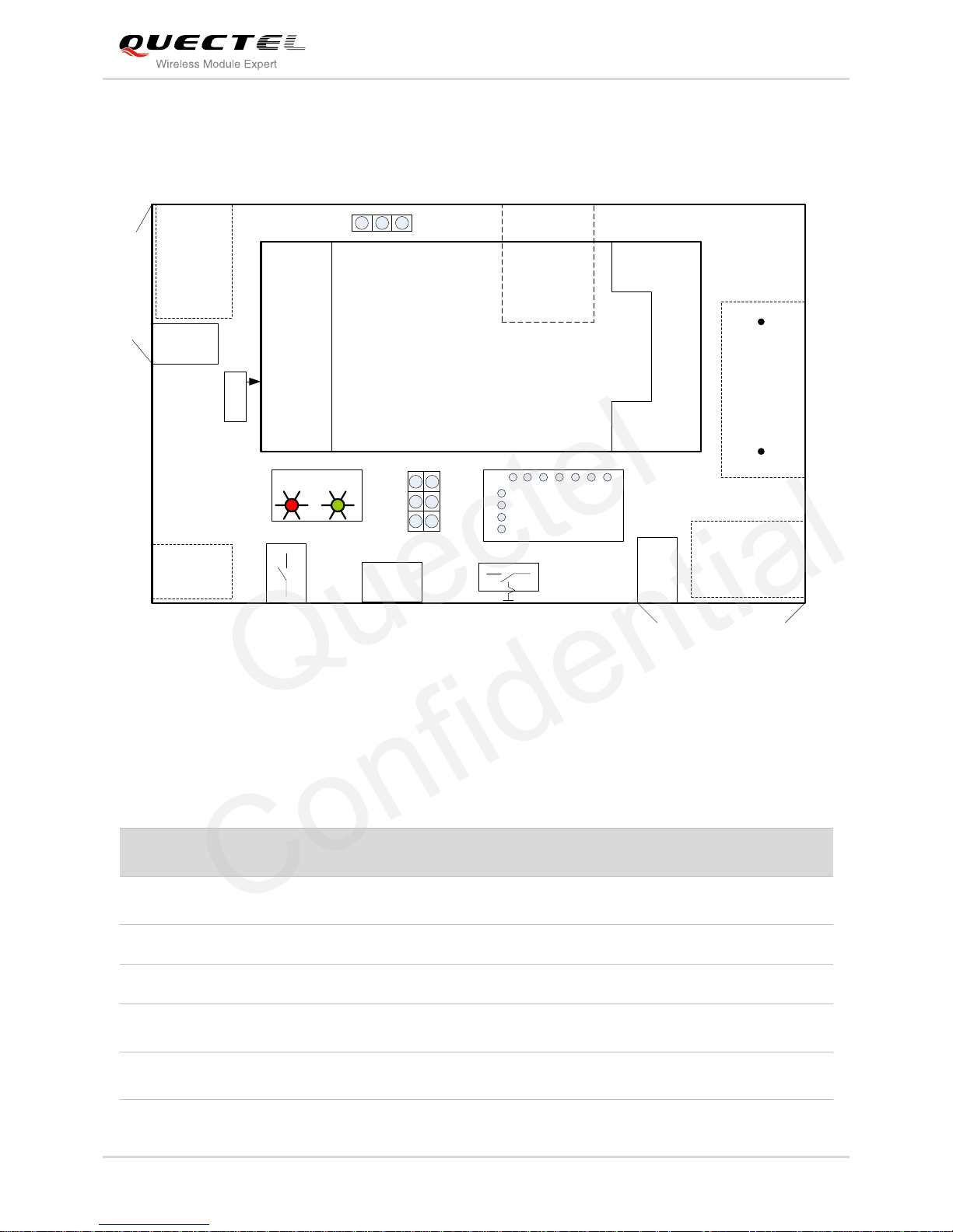
2.3. System Overview
3V3
J202
Mini PCIe card
J301
COM (UART Port)
J201
J302
S201
S101
Micro USB
interface
J303
J404
USIM card holder
Audio interface
Power
supply
Power
switch
RESET
D103 D101
Status LEDs
1 5
6 9
Test points
VBAT
3V 3V
UART PCM
1.8V 1.8V
GND
J304 J405
J103
USB_ON W_DISABLE
J101 J102
1
51252
J401
J403
J402
Audio interface
Figure 1: System Overview
2.4. Interface Overview
Table 2: Interfaces of Mini PCIe EVB
Interface
Reference
Number
Description
Power Supply
J201
(bottom side)
The power jack on the EVB board. Supply voltage typically +5V
Power Switch
S201
Control power supply VBAT ON/OFF
RESET
S101
Reset button. It is used to reset the Mini PCIe module
Micro USB
J302
USB device interface
It can also be used to supply power to EVB board
Audio
J401
Used for Ф3.5mm CTIA earphone by default
Used to test module PCM function
Quectel
Confidential
 Loading...