

Quectel M10 Hardware Description
M10
Quectel Cellular Engine
Hardware Design
M10_HD_V1.00

M10 Hardware Design
Quectel
Document Title
Revision
Date
Status
Document Control ID
General Notes
Quectel offers this information as a service to its customers, to support application and
engineering efforts that use the products designed by Quectel. The information provided is
based upon requirements specifically provided to Quectel by the customers. Quectel has not
undertaken any independent search for additional relevant information, including any
information that may be in the customer’s possession. Furthermore, system validation of this
product designed by Quectel within a larger electronic system remains the responsibility of
the customer or the customer’s system integrator. All specifications supplied herein are
subject to change.
Copyright
This document contains proprietary technical information which is the property of Quectel
Limited., copying of this document and giving it to others and the using or communication of
the contents thereof, are forbidden without express authority. Offenders are liable to the
payment of damages. All rights reserved in the event of grant of a patent or the registration of
a utility model or design. All specification supplied herein are subject to change without
notice at any time.
Copyright © Shanghai Quectel Wireless Solutions Co., Ltd. 2009
M10 Hardware Design
1.00
2009-06-27
Release
M10_HD_V1.00
M10_HD_V1.00 - 1 -

M10 Hardware Design
Quectel
Contents
Contents ............................................................................................................................................2
0 Revision history........................................................................................................................... 7
1 Introduction ..................................................................................................................................8
1.1 Related documents ............................................................................................................... 8
1.2 Terms and abbreviations.......................................................................................................9
1.3 Safety caution..................................................................................................................... 11
2 Product concept ........................................................................................................................13
2.1 Key features .......................................................................................................................13
2.2 Functional diagram.............................................................................................................15
2.3 Evaluation board ................................................................................................................16
3 Application interface.................................................................................................................17
3.1 Pin description....................................................................................................................17
3.2 Operating modes ................................................................................................................20
3.3 Power supply ......................................................................................................................21
3.3.1 Power supply pins ....................................................................................................23
3.3.2 Minimizing power losses..........................................................................................23
3.3.3 Monitoring power supply .........................................................................................23
3.4 Power up and power down scenarios .................................................................................24
3.4.1 Turn on .....................................................................................................................24
3.4.2 Turn off.....................................................................................................................26
3.4.3 Restart module using the PWRKEY pin...................................................................29
3.5 Power saving ......................................................................................................................30
3.5.1 Minimum functionality mode...................................................................................30
3.5.2 SLEEP mode (slow clock mode)..............................................................................31
3.5.3 Wake up module from SLEEP mode .......................................................................31
3.6 Summary of state transitions (except SLEEP mode)..........................................................31
3.7 RTC backup .......................................................................................................................32
3.8 Serial interfaces..................................................................................................................33
3.8.1 Function of serial port & debug port supporting......................................................35
3.8.2 Software upgrade and software debug......................................................................36
3.9 Audio interfaces..................................................................................................................38
3.9.1 Microphone interfaces configuration........................................................................40
3.9.2 Speaker interface configuration................................................................................41
3.9.3 Earphone interface configuration .............................................................................43
3.10 Buzzer ..............................................................................................................................44
3.11 SIM card interface............................................................................................................45
3.11.1 SIM card application ..............................................................................................45
3.11.2 Design considerations for SIM card holder............................................................46
3.12 LCD interface...................................................................................................................48
3.13 Keypad interface ..............................................................................................................49
3.14 ADC..................................................................................................................................50
M10_HD_V1.00 - 2 -

M10 Hardware Design
Quectel
3.15 Behaviors of the RI ..........................................................................................................51
3.16 Network status indication.................................................................................................52
3.17 General purpose input & output (GPIO) ..........................................................................53
3.18 Open drain output (LIGHT_MOS)...................................................................................53
4 Antenna interface......................................................................................................................55
4.1 Antenna installation............................................................................................................55
4.2 RF output power.................................................................................................................55
4.3 RF receive sensitivity.........................................................................................................56
4.4 Operating frequencies ........................................................................................................56
5 Electrical, reliability and radio characteristics....................................................................... 57
5.1 PIN assignment of the module ........................................................................................... 57
5.2 Absolute maximum ratings.................................................................................................59
5.3 Operating temperatures ...................................................................................................... 59
5.4 Power supply ratings ..........................................................................................................59
5.5 Current consumption..........................................................................................................60
5.6 Electro-static discharge ...................................................................................................... 62
6 Product information...................................................................................................................64
7 Mechanics.................................................................................................................................. 65
7.1 Mechanical dimensions of module..................................................................................... 65
7.2 Footprint of recommendation.............................................................................................67
7.3 Top view of the module .....................................................................................................69
7.4 Bottom view of the module................................................................................................ 69
M10_HD_V1.00 - 3 -

M10 Hardware Design
Quectel
Table Index
TABLE 1: RELATED DOCUMENTS.....................................................................................................8
TABLE 2: TERMS AND ABBREVIATIONS ......................................................................................... 9
TABLE 3: MODULE KEY FEATURES................................................................................................13
TABLE 4: CODING SCHEMES AND MAXIMUM NET DATA RATES OVER AIR INTERFACE .. 15
TABLE 5: PIN DESCRIPTION .............................................................................................................17
TABLE 6: OVERVIEW OF OPERATING MODES..............................................................................20
TABLE 7: AT COMMANDS USED IN ALARM MODE .....................................................................26
TABLE 8: SUMMARY OF STATE TRANSITIONS.............................................................................31
TABLE 9: LOGIC LEVELS OF THE SERIAL PORT AND DEBUG PORT .......................................34
TABLE 10: PIN DEFINITION OF THE SERIAL INTERFACES ........................................................34
TABLE 11: PIN DEFINITION OF AUDIO INTERFACE .................................................................... 39
TABLE 12: MIC INPUT CHARACTERISTICS...................................................................................43
TABLE 13: SPK OUTPUT CHARACTERISTICS ...............................................................................43
TABLE 14: PIN DEFINITION OF THE BUZZER ...............................................................................44
TABLE 15: BUZZER OUTPUT CHARACTERISTICS ....................................................................... 44
TABLE 16: PIN DEFINITION OF THE SIM INTERFACE .................................................................45
TABLE 17: PIN DESCRIPTION (AMPHENOL SIM CARD HOLDER) ............................................ 47
TABLE 18: PIN DESCRIPTION (MOLEX SIM CARD HOLDER) ....................................................48
TABLE 19: PIN DEFINITION OF THE LCD INTERFACE ................................................................49
TABLE 20: PIN DEFINITION OF THE KEYPAD INTERFACE ........................................................49
TABLE 21: PIN DEFINITION OF THE ADC.......................................................................................51
TABLE 22: CHARACTERISTICS OF THE ADC ................................................................................51
TABLE 23: BEHAVIOURS OF THE RI................................................................................................51
TABLE 24: WORKING STATE OF THE NETLIGHT .........................................................................52
TABLE 25: PIN DEFINITION OF THE GPIO INTERFACE ............................................................... 53
TABLE 26: PIN DEFINITION OF THE LIGHT_MOS ........................................................................54
TABLE 27: PIN DEFINITION OF THE RF_ANT................................................................................ 55
TABLE 28: THE MODULE CONDUCTED RF OUTPUT POWER ....................................................55
TABLE 29: THE MODULE CONDUCTED RF RECEIVE SENSITIVITY ........................................56
TABLE 30: THE MODULE OPERATING FREQUENCIES................................................................56
TABLE 31: M10 CONNECTION DIAGRAMS....................................................................................58
TABLE 32: ABSOLUTE MAXIMUM RATINGS.................................................................................59
TABLE 33: OPERATING TEMPERATURE......................................................................................... 59
TABLE 34: THE MODULE POWER SUPPLY RATINGS................................................................... 59
TABLE 35: THE MODULE CURRENT CONSUMPTION..................................................................60
TABLE 36: THE ESD ENDURE STATUE MEASURED TABLE (TEMPERATURE: 25℃,
HUMIDITY: 45 %) ........................................................................................................................ 62
TABLE 37: ORDERING INFORMATION ...........................................................................................64
M10_HD_V1.00 - 4 -

M10 Hardware Design
Quectel
Figure Index
FIGURE 1: MODULE FUNCTIONAL DIAGRAM .............................................................................16
FIGURE 2: REFERENCE CIRCUIT OF THE VBAT INPUT ..............................................................22
FIGURE 3: REFERENCE CIRCUIT OF THE SOURCE POWER SUPPLY INPUT...........................22
FIGURE 4: POWER SUPPLY LIMITS DURING TRANSMITTING BURST .................................... 23
FIGURE 5: TURN ON THE MODULE USING DRIVING CIRCUIT.................................................24
FIGURE 6: TURN ON THE MODULE USING KEYSTROKE...........................................................25
FIGURE 7: TIMING OF TURN ON SYSTEM ..................................................................................... 25
FIGURE 8: TIMING OF TURN OFF SYSTEM ...................................................................................27
FIGURE 9: REFERENCE CIRCUIT FOR EMERG_OFF USING DRIVING CIRCUIT .................... 28
FIGURE 10: REFERENCE CIRCUIT FOR EMERG_OFF USING KEYSTOKE ...............................29
FIGURE 11 : TIMING OF RESTART SYSTEM...................................................................................29
FIGURE 12 : TIMING OF RESTART SYSTEM AFTER EMERGENCY SHUTDOWN.................... 30
FIGURE 13: RTC SUPPLY FROM NON-CHARGEABLE BATTERY ...............................................32
FIGURE 14: RTC SUPPLY FROM RECHARGEABLE BATTERY ....................................................32
FIGURE 15: RTC SUPPLY FROM CAPACITOR ................................................................................33
FIGURE 16: SEIKO XH414H-IV01E CHARGE CHARACTERISTIC ...............................................33
FIGURE 17: CONNECTION OF SERIAL INTERFACES ...................................................................35
FIGURE 18: CONNECTION OF SOFTWARE UPGRADE.................................................................37
FIGURE 19: CONNECTION OF SOFTWARE DEBUG......................................................................37
FIGURE 20: RS232 LEVEL CONVERTER CIRCUIT .........................................................................38
FIGURE 21: MICROPHONE INTERFACE CONFIGURATION OF AIN1&AIN2 ............................40
FIGURE 22: SPEAKER INTERFACE CONFIGURATION OF AOUT1 ............................................. 41
FIGURE 23: SPEAKER INTERFACE WITH AMPLIFIER CONFIGURATION OF AOUT1 ............41
FIGURE 24: SPEAKER INTERFACE CONFIGURATION OF AOUT2 ............................................. 42
FIGURE 25: SPEAKER INTERFACE WITH AMPLIFIER CONFIGURATION OF AOUT2 ............42
FIGURE 26: EARPHONE INTERFACE CONFIGURATION..............................................................43
FIGURE 27: REFERENCE CIRCUIT FOR BUZZER..........................................................................44
FIGURE 28: REFERENCE CIRCUIT OF THE 8 PINS SIM CARD....................................................46
FIGURE 29: REFERENCE CIRCUIT OF THE 6 PINS SIM CARD....................................................46
FIGURE 30: AMPHENOL C707 10M006 512 2 SIM CARD HOLDER.............................................. 47
FIGURE 31: MOLEX 91228 SIM CARD HOLDER ............................................................................48
FIGURE 32: REFERENCE CIRCUIT OF THE KEYPAD INTERFACE.............................................50
FIGURE 33: INTERNAL CIRCUIT OF THE ADC..............................................................................51
FIGURE 34: MODULE SERVICES AS RECEIVER............................................................................52
FIGURE 35 : MODULE SERVICES AS CALLER...............................................................................52
FIGURE 36: REFERENCE CIRCUIT OF THE NETLIGHT................................................................53
FIGURE 37: REFERENCE CIRCUIT OF THE LIGHT_MOS.............................................................54
FIGURE 38: M10 TOP AND SIDE DIMENSIONS(UNIT: MM)....................................................65
FIGURE 39: M10 BOTTOM DIMENSIONS(UNIT: MM) .............................................................66
M10_HD_V1.00 - 5 -

M10 Hardware Design
Quectel
FIGURE 40: PAD BOTTOM DIMENSIONS(UNIT: MM) .............................................................66
FIGURE 41: FOOTPRINT OF RECOMMENDATION(UNIT: MM)..............................................68
FIGURE 42: TOP VIEW OF THE MODULE .......................................................................................69
FIGURE 43: BOTTOM VIEW OF THE MODULE..............................................................................69
M10_HD_V1.00 - 6 -

M10 Hardware Design
Quectel
0 Revision history
Revision Date Author Description of change
1.00 2009-06-27 Tracy ZHANG Initial
M10_HD_V1.00 - 7 -
M10 Hardware Design
Quectel
1 Introduction
This document defines and specifies the M10 module series. For detail product information,
please refer to the chapter 6
of the Quectel’s M10 module series that connects to the specific application and the air interface.
This document can help you quickly understand module interface specifications, electrical and
mechanical details. With the help of this document and other M10 application notes, user guide,
you can use M10 module to design and set up mobile applications quickly.
1.1 Related documents
Table 1: Related documents
Product Information.This document describes the hardware interface
SN Document name Remark
[ 1 ] M1 0 _ AT C AT co m m a n d s s e ts
[2] ITU-T Draft new
recommendation
V.25ter:
[3] GSM 07.07: Digital cellular telecommunications (Phase 2+); AT command
[4] GSM 07.10: Support GSM 07.10 multiplexing protocol
[5] GSM 07.05: Digital cellular telecommunications (Phase 2+); Use of Data
[6] GSM 11.14: Digital cellular telecommunications system (Phase 2+);
[7] GSM 11.11: Digital cellular telecommunications system (Phase 2+);
[8] GSM 03.38: Digital cellular telecommunications system (Phase 2+);
[9] GSM 11.10 Digital cellular telecommunications system (Phase 2) ;
[10] GSM_UART_AN The document of UART port application notes
[11] M10_HD_AN01 The document of M10 hardware design application notes
Serial asynchronous automatic dialing and control
set for GSM Mobile Equipment (ME)
Terminal Equipment – Data Circuit terminating Equipment
(DTE – DCE) interface for Short Message Service (SMS) and
Cell Broadcast Service (CBS)
Specification of the SIM Application Toolkit for the Subscriber
Identity module – Mobile Equipment (SIM – ME) interface
Specification of the Subscriber Identity module – Mobile
Equipment (SIM – ME) interface
Alphabets and language-specific information
Mobile Station (MS) conformance specification ; Part 1:
Conformance specification
M10_HD_V1.00 - 8 -
M10 Hardware Design
Quectel
1.2 Terms and abbreviations
Table 2: Terms and abbreviations
Abbreviation Description
ADC Analog-to-Digital Converter
AMR Adaptive Multi-Rate
ARP Antenna Reference Point
ASIC Application Specific Integrated Circuit
BER Bit Error Rate
BTS Base Transceiver Station
CHAP Challenge Handshake Authentication Protocol
CS Coding Scheme
CSD Circuit Switched Data
CTS Clear to Send
DAC Digital-to-Analog Converter
DRX Discontinuous Reception
DSP Digital Signal Processor
DTE Data Terminal Equipment (typically computer, terminal, printer)
DTR Data Terminal Ready
DTX Discontinuous Transmission
EFR Enhanced Full Rate
EGSM Enhanced GSM
EMC Electromagnetic Compatibility
ESD Electrostatic Discharge
ETS European Telecommunication Standard
FCC Federal Communications Commission (U.S.)
FDMA Frequency Division Multiple Access
FR Full Rate
GMSK Gaussian Minimum Shift Keying
GPRS General Packet Radio Service
GSM Global Standard for Mobile Communications
HR Half Rate
I/O Input/Output
IC Integrated Circuit
IMEI International Mobile Equipment Identity
Inorm Normal Current
Imax Maximum Load Current
kbps Kilo bits per second
LED Light Emitting Diode
Li-Ion Lithium-Ion
ESD Electro-Static discharge
M10_HD_V1.00 - 9 -
M10 Hardware Design
Quectel
Abbreviation Description
MO Mobile Originated
MS Mobile Station (GSM engine), also referred to as TE
MT Mobile Terminated
PAP Password Authentication Protocol
PBCCH Packet Switched Broadcast Control Channel
PCB Printed Circuit Board
PDU Protocol Data Unit
PPP Point-to-point protocol
RF Radio Frequency
RMS Root Mean Square (value)
RTC Real Time Clock
Rx Receive Direction
SIM Subscriber Identification Module
SMS Short Message Service
TDMA Time Division Multiple Access
TE Terminal Equipment, also referred to as DTE
TX Transmitting Direction
UART Universal Asynchronous Receiver & Transmitter
URC Unsolicited Result Code
USSD Unstructured Supplementary Service Data
VSWR Voltage Standing Wave Ratio
Vmax Maximum Voltage Value
Vnorm Normal Voltage Value
Vmin Minimum Voltage Value
VIHmax Maximum Input High Level Voltage Value
VIHmin Minimum Input High Level Voltage Value
VILmax Maximum Input Low Level Voltage Value
VILmin Minimum Input Low Level Voltage Value
VImax Absolute Maximum Input Voltage Value
VImin Absolute Minimum Input Voltage Value
VOHmax Maximum Output High Level Voltage Value
VOHmin Minimum Output High Level Voltage Value
VOLmax Maximum Output Low Level Voltage Value
VOLmin Minimum Output Low Level Voltage Value
Phonebook abbreviations
FD SIM fix dialing phonebook
LD SIM last dialing phonebook (list of numbers most recently dialed)
MC Mobile Equipment list of unanswered MT calls (missed calls)
ON SIM (or ME) own numbers (MSISDNs) list
M10_HD_V1.00 - 10 -
M10 Hardware Design
p
Quectel
Abbreviation Description
RC Mobile Equipment list of received calls
SM SIM phonebook
FWP Fixed Wireless Phone
FWT Fixed Wireless Terminal
NC Not connect
1.3 Safety caution
The following safety precautions must be observed during all phases of the operation. Usage ,
service or repair of any cellular terminal or mobile incorporating M10 module. Manufactures of
the cellular terminal should send words the following safety information to users and operating
personnel and to incorporate these guidelines into all manuals supplied with the product. If not so,
Quectel does not take on any liability for customer failure to comply with these precautions.
When in a hospital or other health care facility, observe the restrictions about the
use of mobiles. Switch the cellular terminal or mobile off, medical equipment
may be sensitive to not operate normally for RF energy interference.
Switch off the cellular terminal or mobile before boarding an aircraft.
Make sure it be switched off. The operation of wireless appliances in an
aircraft is forbidden to prevent interference with communication systems.
Forget to think much of these instructions may lead to the flight safety or
offend against local legal action, or both.
Do not operate the cellular terminal or mobile in the presence of flammable
gases or fumes. Switch off the cellular terminal when you are near petrol
stations, fuel depots, chemical plants or where blasting operations are in
progress. Operation of any electrical equipment in potentially explosive
atmos
heres can constitute a safety hazard.
Your cellular terminal or mobile receives and transmits radio frequency
energy while switched on. RF interference can occur if it is used close to TV
sets, radios, computers or other electric equipment.
Road safety comes first! Do not use a hand-held cellular terminal or mobile
when driving a vehicle, unless it is securely mounted in a holder for
handsfree operation. Before making a call with a hand-held terminal or
mobile, park the vehicle.
M10_HD_V1.00 - 11 -

M10 Hardware Design
Quectel
GSM cellular terminals or mobiles operate over radio frequency signals and
cellular networks and cannot be guaranteed to connect in all conditions, for
example no mobile fee or a invalid SIM card. While you are in this condition
and need emergent help, Please Remember using emergency calls. In order to
make or receive calls, the cellular terminal or mobile must be switched on
and in a service area with adequate cellular signal strength.
Some networks do not allow for emergency call if certain network services
or phone features are in use (e.g. lock functions, fixed dialing etc.). You may
have to deactivate those features before you can make an emergency call.
Also, some networks require that a valid SIM card be properly inserted in the
cellular terminal or mobile.
M10_HD_V1.00 - 12 -
M10 Hardware Design
Quectel
2 Product concept
The M10 is a Quad-band GSM/GPRS engine that works at frequencies GSM850, EGSM 900
MHz, DCS 1800 MHz and PCS 1900 MHz. The M10 features GPRS multi-slot class 12(default)/
class 10/class8 and supports the GPRS coding schemes CS-1, CS-2, CS-3 and CS-4.
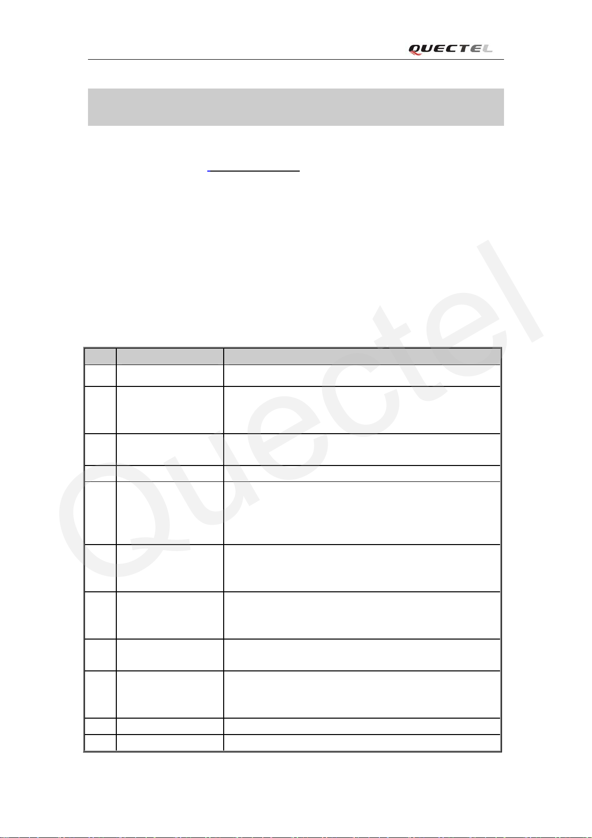
With a tiny profile of 29mm x 29mm x 3.6 mm(the thickness of PCB is 1.6mm), the module can
meet almost all the requirements, such as M2M, Telemetry and other mobile data communication
systems.
The M10 is a an SMD type module, which can be embedded in customer applications through it’s
64-pin pads. It provides all hardware interfaces between the module and customers’ boards.
z The keypad and LCD interface are flexible to develop customized applications.
z Serial port can help you easily develop your applications.
z Two audio channels include two microphone inputs and two speaker outputs. This can be
easily configured by AT command.
The module is designed with power saving technique so that the current consumption is as low as
1.1 mA in SLEEP mode.
The M10 is integrated with the TCP/IP protocol; extended TCP/IP AT commands are developed
for customers to use the TCP/IP protocol easily, which is very useful for those data transfer
applications.
The modules are fully RoHS compliant to EU regulation.
2.1 Key features
Table 3: Module key features
Feature Implementation
Power supply Single supply voltage 3.4V – 4.5V
Power saving Typical power consumption in SLEEP mode to 1.1 mA@ DRX=5
0.7 mA@ DRX=9
Frequency bands
GSM class Small MS
Transmitting power z Class 4 (2W) at GSM 850 and EGSM 900
M10_HD_V1.00 - 13 -
z Quad-band: GSM850, EGSM 900, DCS1800, PCS1900.
z The module can search these frequency bands automatically.
The frequency bands also can be set by AT command.
z Compliant to GSM Phase 2/2+
M10 Hardware Design
Quectel
z Class 1 (1W) at DCS 1800 and PCS 1900
GPRS connectivity
Temperature range
DATA GPRS:
CSD:
SMS z MT, MO, CB, Text and PDU mode
FAX Group 3 Class 1
SIM interface Support SIM card: 1.8V, 3V
Antenna interface Connected via 50 Ohm antenna pad
Audio features Speech codec modes:
Serial port and Debug port z Serial Port: Seven lines on Serial Port Interface
Phonebook management Support phonebook types: SM, FD, LD, RC, ON, MC.
SIM Application Toolkit Support SAT class 3, GSM 11.14 Release 99
Real time clock Implemented
Alarm function Programmable via AT command
Physical characteristics Size:
z GPRS multi-slot class 12 (default)
z GPRS multi-slot class 10 (option)
z GPRS multi-slot class 8 (option)
z GPRS mobile station class B
z Normal operation: -35°C ~ +80°C
1
z Restricted operation: -45°C ~ -35°C and +80°C ~ +85°C
z Storage temperature: -45°C ~ +90°C
z GPRS data downlink transfer: max. 85.6 kbps
z GPRS data uplink transfer: max. 85.6 kbps
z Coding scheme: CS-1, CS-2, CS-3 and CS-4
z Supports the protocols PAP (Password Authentication Protocol)
usually used for PPP connections.
z Integrates the TCP/IP protocol.
z Support Packet Switched Broadcast Control Channel (PBCCH)
z CSD transmission rates: 2.4, 4.8, 9.6, 14.4 kbps,
non-transparent
z Unstructured Supplementary Services Data (USSD) support
z SMS storage: SIM card
z Half Rate (ETS 06.20)
z Full Rate (ETS 06.10)
z Enhanced Full Rate (ETS 06.50 / 06.60 / 06.80)
z Adaptive multi rate (AMR)
z Echo Cancellation
z Echo Suppression
z Noise Reduction
z Serial Port can be used for CSD FAX, GPRS service and send
AT command of controlling module.
z Serial Port can use multiplexing function.
z Autobauding supports baud rate from 4800 bps to 115200bps.
z Debug Port: Two lines on Serial Port Interface /TXD and /RXD
z Debug Port only used for debugging
○
M10_HD_V1.00 - 14 -
M10 Hardware Design
Quectel
29±0.15 x 29±0.15 x 3.6±0.3mm
Weight: 8g
Firmware upgrade Firmware upgrade over serial port
1
○
When the module works in this temperature range, the deviations from the GSM specification
might occur. For example, the frequency error or the phase error could increase.
Table 4: Coding schemes and maximum net data rates over air interface
Coding scheme 1 Timeslot 2 Timeslot 4 Timeslot
CS-1: 9.05kbps 18.1kbps 36.2kbps
CS-2: 13.4kbps 26.8kbps 53.6kbps
CS-3: 15.6kbps 31.2kbps 62.4kbps
CS-4: 21.4kbps 42.8kbps 85.6kbps
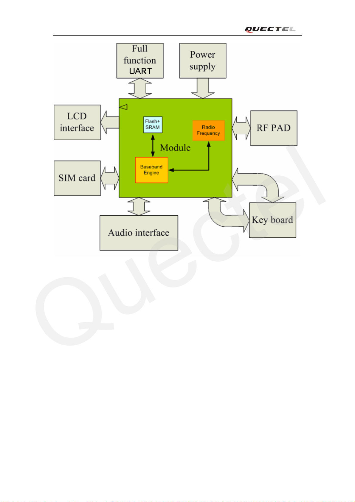
2.2 Functional diagram
The following figure shows a block diagram of the M10 module and illustrates the major
functional part:
z The GSM baseband engine
z Flash and SRAM
z The GSM radio frequency part
z The SMT pads interface
—LCD interface
—SIM card interface
—Audio interface
—Key board interface
—UART interface
—Power supply
—RF interface
M10_HD_V1.00 - 15 -
M10 Hardware Design
Quectel
Figure 1
2.3 Evaluation board
In order to help you on the application of M10, Quectel can supply an Evaluation Board (EVB)
and a link-board that interfaces the module directly with appropriate power supply, SIM card
holder, RS232 serial interface, handset port, earphone port, antenna and all GPIOs of the module.
For details, please refer to the M10_EVB_UGD document.
: Module functional diagram
M10_HD_V1.00 - 16 -
M10 Hardware Design
Quectel
3 Application interface
The module is equipped with a 64-pin 1.3mm pitch SMT pad that connects to the cellular
application platform. Sub-interfaces included in these pads are described in detail in following
chapters:
z Power supply (
z Serial interfaces (
z Two analog audio interfaces (
z SIM interface (refer to Chapter 3.11)
Electrical and mechanical characteristics of the SMT pad are specified in Chapter 5&Chapter7.
3.1 Pin description
refer to Chapter 3.3)
refer to Chapter 3.8)
refer to Chapter 3.9)
Table 5: Pin description
Power Supply
PIN NAME I/O DESCRIPTION DC CHARACTERISTICS COMMENT
VBAT I VBAT pins of the SMT pad
are dedicated to connect the
supply voltage. The power
supply of module has to be a
single voltage source of
VBAT= 3.4V...4.5V. It must
be able to provide sufficient
current in a transmitting
burst which typically rises to
2A.mostly, These 3 pins are
voltage inputs.
VRTC I/O Current input for RTC when
the battery is not supplied for
the system.
Current output for backup
battery when the main
battery is present and the
backup battery is in low
voltage state.
VDD_EXT O Supply 2.8V voltage for
external circuit. By
measuring this pin, user can
Vmax= 4.5V
Vmin=3.4V
Vnorm=4.0V
Vmax=2.85V
Vmin=2.6V
Vnorm=2.75V
Iout(max)= 730uA
Iin=2.6~5 uA
Vmax=2.9V
Vmin=2.7V
Vnorm=2.8V
Recommend to
connected to a
battery or a
capacitor.
1.If unused,keep
pin open.
2. Recommend
M10_HD_V1.00 - 17 -
M10 Hardware Design
Quectel
judge whether the system is
power on or off. When the
voltage is low, the system is
power off. Otherwise, the
system is power on.
GND Digital ground
Power on or power off
PIN NAME I/O DESCRIPTION DC CHARACTERISTICS COMMENT
PWRKEY I Voltage input for power
on/off key. PWRKEY should
be pulled down to turn on or
turn off the system. The user
should keep pressing the key
for a moment when turn on
or turn off the system.
Because the system need
margin time in order to assert
the software.
Emergency shutdown
PIN NAME I/O DESCRIPTION DC CHARACTERISTICS COMMENT
EMERG_OFF I Voltage input for emergency
shutdown under emergent
situation. EMERG_OFF
should be pulled down for at
least 20ms to emergency
shutdown the system. The
module can restart if
PWRKEY is activated after
emergency shutdown.
Audio interfaces
Imax=20mA
VILmax=0.3*VBAT
VIHmin=0.7*VBAT
VImax=VBAT
VILmax=0.4V
VIHmin=2.2V
V
max=2.8V
open
to add a
2.2~4.7uF bypass
capacitor, when
using this pin for
power supply.
Pull up to VBAT
Internally.
Open
drain/collector
driver required in
cellular device
application.
If unused keep
pin open.
PIN NAME I/O DESCRIPTION DC CHARACTERISTICS COMMENT
MIC1P
MIC1N
MIC2P
MIC2N
SPK1P
SPK1N
SPK2P O Auxiliary positive
AGND AGND is separate ground
BUZZER O Buzzer output If unused keep
M10_HD_V1.00 - 18 -
I Positive and negative
voice-band input
I Auxiliary positive and
negative voice-band input
O Positive and negative
voice-band output
voice-band output
connection for external audio
circuits.
Audio DC Characteristics
refer to chapter 3.9.4
If unused keep
If unused keep
If unused keep
pins open
pin open
pins open.
M10 Hardware Design
Quectel
pin open
General purpose input/output
PIN NAME I/O DESCRIPTION DC CHARACTERISTICS COMMENT
KBC0~KBC4 I If unused keep
KBR0~KBR4 O
DISP_DATA I/O
DISP_CLK O
DISP_CS O
DISP_D/C O
DISP_RST O
NETLIGHT O Network status indication
GPIO0 I/O Normal input/output port
GPIO1_KBC5 I/O Normal input/output
LIGHT_MOS O Open drain output port Imax=100mA If unused keep
Serial port
PIN NAME I/O DESCRIPTION DC CHARACTERISTICS COMMENT
DTR I Data terminal ready
RXD I Receive data
TXD O Transmitting data
RTS I Request to send
CTS O Clear to send
RI O Ring indicator
DCD O Data carrier detection
Debug port
DBG_TXD O
DBG_RXD I
Keypad interface
LCD display interface If unused keep
port/Keypad interface
Serial interface for
debugging only.
VILmin=0V
VILmax=0.67V
VIHmin=1.7V
VIHmax= VDD_EXT+0.3
VOLmin=GND
VOLmax=0.34V
VOHmin=2.0V
VOHmax= VDD_EXT
VILmin=0V
VILmax=0.67V
VIHmin=1.7V
VIHmax= VDD_EXT+0.3
VOLmin=GND
VOLmax=0.34V
VOHmin=2.0V
VOHmax= VDD_EXT
pins open
Pull up to
VDD_EXT, if
unused keep pins
open
pins open
If unused keep
pins open
pin open
If only use TXD
RXD GND to
communicate,
RTS pin should
connect to GND
directly.
If unused keep
pins open.
If unused keep
pins open
SIM interface
PIN NAME I/O DESCRIPTION DC CHARACTERISTICS COMMENT
SIM_VDD O Voltage supply for SIM card The voltage can be
selected by software
automatically either 1.8V
or 3V
SIM_DATA I/O SIM data output
SIM_CLK O SIM clock
M10_HD_V1.00 - 19 -
VIHmin=0.7*SIM_VDD
VOHmin=0.8*SIM_VDD
All signals of
SIM interface
should be
protected against
ESD with a TVS
diode array.
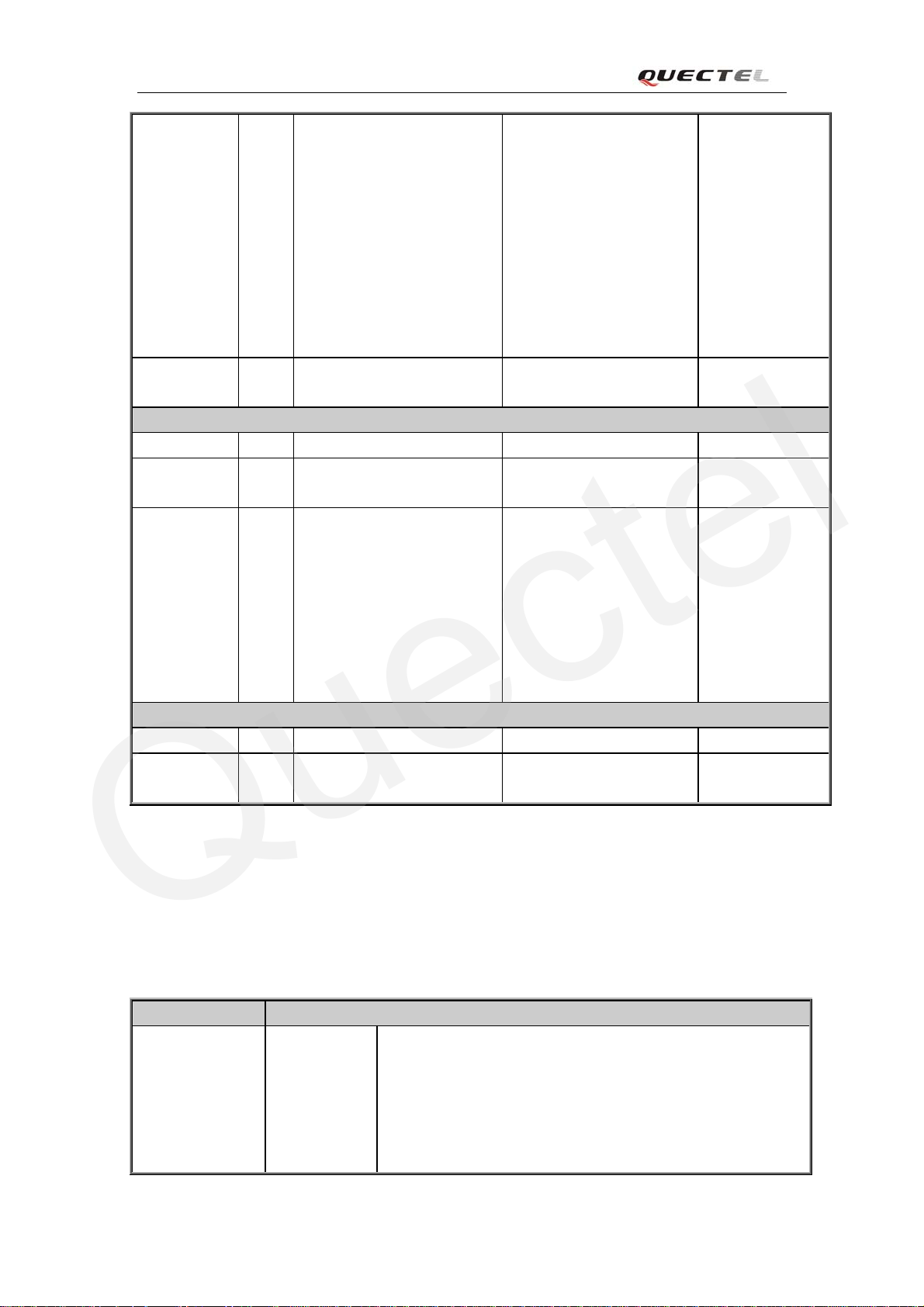
M10 Hardware Design
Quectel
SIM_RST O SIM reset VOLmax=0.4V
When SIM_VDD=3V
VILmax=0.4V
When SIM_VDD=1.8V
VILmax=0.2* SIM_VDD
VOHmin=0.9*SIM_VDD
When SIM_VDD=3V
VOLmax=0.4V
When SIM_VDD=1.8V
VOLmax=0.2* SIM_VDD
SIM_PRESE
NCE
AUXADC
PIN NAME I/O DESCRIPTION DC CHARACTERISTICS COMMENT
ADC0 I General purpose analog to
TEMP_BAT I ADC input for battery
RF interface
PIN NAME I/O DESCRIPTION DC CHARACTERISTICS COMMENT
RF_ANT I/O RF antenna pad. impedance of 50Ω Refer to chapter
I SIM card detection VILmax=0.67V
VIHmin=1.7V
voltage range: 0V to 2.8V If unused keep
digital converter.
voltage range: 0V to 2.8V NTC should be
temperature over NTC
resistor.
Maximum cable
length 200mm
from the module
pad to SIM card
holder.
If unused , keep
pin open.
pin open
installed inside
or near battery
pack to deliver
temperature
values.
If unused keep
pin open.
4
3.2 Operating modes
The table below briefly summarizes the various operating modes referred to in the following
chapters.
Table 6: Overview of operating modes
Mode Function
Normal operation GSM/GPRS
SLEEP
M10_HD_V1.00 - 20 -
The module will automatically go into SLEEP mode if DTR is
set to high level and there is no interrupt (such as GPIO
interrupt or data on serial port).
In this case, the current consumption of module will reduce to
the minimal level.
During SLEEP mode, the module can still receive paging
M10 Hardware Design
Quectel
message and SMS from the system normally.
GSM IDLE Software is active. The module has registered to the GSM
network, and the module is ready to send and receive.
GSM TALK Connection is going on between two subscribers. In this case,
the power consumption depends on network settings such as
DTX off/on, FR/EFR/HR, hopping sequences.
GPRS
STANDBY
GPRS DATA There is GPRS data in transfer (PPP or TCP or UDP). In this
POWER DOWN Normal shutdown by sending the “AT+QPOWD=1” command, using the
PWRKEY or using the EMERG_OFF
disconnects the power supply from the base band part of the module, and only
the power supply for the RTC is remained. Software is not active. The serial
interfaces are not accessible. Operating voltage (connected to VBAT) remains
applied.
Minimum
functionality
mode (without
remove power
supply)
Alarm mode RTC alert function launches this restricted operation while the module is in
Use the “AT+CFUN” command can set the module to a minimum functionality
mode without remove the power supply. In this case, the RF part of the module
will not work or the SIM card will not be accessible, or both RF part and SIM
card will be closed all, and the serial interface is still accessible. The power
consumption in this case is very low.
POWER DOWN mode. The module will not be registered to GSM network and
only parts of AT commands can be available.
The module is ready for GPRS data transfer, but no data is
currently sent or received. In this case, power consumption
depends on network settings and GPRS configuration.
case, power consumption is related with network settings (e.g.
power control level), uplink / downlink data rates and GPRS
configuration (e.g. used multi-slot settings).
①. The power management ASIC
①Use the EMERG_OFF only when, due to serious problems. Please refer to chapter3.4.2.4.
3.3 Power supply
The power supply of module is from a single voltage source of VBAT= 3.4V...4.5V. In some case,
the ripple in a transmitting burst may cause voltage drops when current consumption rise to
typical peaks of 2A. So the power supply must be able to provide sufficient current up to 2A.For
the VBAT input, a local bypass capacitor is recommended. A capacitor (about 100 µF, low ESR)
is recommended. Multi-layer ceramic chip (MLCC) capacitors can provide the best combination
of low ESR and small size but may not be cost effective. A lower cost choice may be a 100 µF
tantalum capacitor (low ESR) with a small (0.1µF to 1µF) ceramic in parallel, which is illustrated
as following figure. The capacitors should put as close as possible to the M10 VBAT pins. The
following figure is the recommended circuit.
M10_HD_V1.00 - 21 -
 Loading...