

Quectel L50 Hardware Design
L50 Hardware Design
L50
Quectel GPS Engine
Hardware Design
L50_HD_V1.0
L50 Hardware Design
Document Title
L50 Hardware Design
Revision
1.0
Date
2011-7-25
Status
Preliminary
Document Control ID
L50_HD_V1.0
Quectel
Preliminary
General Notes
Quectel offers this information as a service to its customers, to support application and
engineering efforts that use the products designed by Quectel. The information provided is
based upon requirements specifically provided for customers of Quectel. Quectel has not
undertaken any independent search for additional information, relevant to any information that
may be in the customer’s possession. Furthermore, system validation of this product designed
by Quectel within a larger electronic system remains the responsibility of the customer or the
customer’s system integrator. All specifications supplied herein are subject to change.
Copyright
This document contains proprietary technical information of Quectel Co., Ltd. Copying of this
document, distribution to others and communication of the contents thereof, are forbidden
without permission. Offenders are liable to the payment of damages. All rights are reserved in
the event of a patent grant or registration of a utility model or design. All specification supplied
herein are subject to change without notice at any time.
Copyright © Quectel Wireless Solutions Co., Ltd. 2011
L50_HD_V1.0 -1 -

L50 Hardware Design
Quectel
Preliminary
Contents
Contents ............................................................................................................................................ 2
Table Index ........................................................................................................................................ 4
Figure Index ...................................................................................................................................... 5
0. Revision History ........................................................................................................................... 6
1. Introduction ................................................................................................................................... 7
1.1 Related Documents ................................................................................................................. 7
1.2 Terms and Abbreviations ......................................................................................................... 7
2. Product Concept ............................................................................................................................ 9
2.1 Key Features ............................................................................................................................ 9
2.2 Functional Diagram ............................................................................................................... 11
2.3 Evaluation Board ................................................................................................................... 11
2.4 Protocol ................................................................................................ ................................. 11
3. Application .................................................................................................................................. 12
3.1 Pin Assignment of the Module .............................................................................................. 12
3.2 Pin Description ...................................................................................................................... 13
3.3 Operating Modes ................................................................................................................... 16
3.4 Power Management ............................................................................................................... 16
3.4.1 VCC Power.................................................................................................................. 16
3.4.2 VIO/RTC Power .......................................................................................................... 16
3.4.3 Energy Saving Mode ................................................................................................... 17
3.5 Power Supply ........................................................................................................................ 18
3.5.1 Power Reference Design ............................................................................................. 18
3.5.2 Battery ......................................................................................................................... 19
3.6 Timing Sequence ................................................................................................................... 20
3.7 Communication Interface ................................................................................................ ...... 22
3.7.1 UART Interface ........................................................................................................... 22
3.7.2 I2C Interface ................................................................................................................ 23
3.7.3 SPI Interface ................................................................................................................ 25
3.8 Assisted GPS ......................................................................................................................... 25
4. Radio Frequency ................................................................................................ ......................... 27
4.1 Antenna ................................................................................................................................. 27
4.2 Design notice ......................................................................................................................... 28
5. Electrical, Reliability and Radio Characteristics ......................................................................... 30
5.1 Absolute Maximum Ratings .................................................................................................. 30
5.2 Operating Conditions ............................................................................................................ 30
5.3 Current Consumption ............................................................................................................ 31
5.4 Electro-Static Discharge ........................................................................................................ 31
5.5 Reliability Test ...................................................................................................................... 32
6. Mechanical Dimensions .............................................................................................................. 33
6.1 Mechanical Dimensions of the Module ................................................................................. 33
6.2 Recommended Footprint ....................................................................................................... 34
6.3 Top View of the Module ....................................................................................................... 35
6.4 Bottom View of the Module .................................................................................................. 35
L50_HD_V1.0 -2 -

L50 Hardware Design
Quectel
Preliminary
7. Manufacturing ............................................................................................................................. 36
7.1 Assembly and Soldering ........................................................................................................ 36
7.2 Moisture Sensitivity .............................................................................................................. 36
7.3 ESD Safe ............................................................................................................................... 37
7.4 Tape and Reel ........................................................................................................................ 37
L50_HD_V1.0 -3 -

L50 Hardware Design
Quectel
Preliminary
Table Index
TABLE 2: TERMS AND ABBREVIATIONS ......................................................................................... 7
TABLE 3: MODULE KEY FEATURES ................................................................ .................................. 9
TABLE 4: THE MODULE SUPPORTS PROTOCOLS ........................................................................ 11
TABLE 5: PIN DESCRIPTION ............................................................................................................. 13
TABLE 6: OVERVIEW OF OPERATING MODES.............................................................................. 16
TABLE 7: PIN DEFINITION OF THE VCC PIN ................................................................................. 16
TABLE 8: PIN DEFINITION OF THE VIO/RTC PIN .......................................................................... 17
TABLE 9: MULTIPLEXED FUNCTION PINS FOR COMMUNICATION INTERFACE .................. 22
TABLE 10: RECOMMENDED EEPROMS .......................................................................................... 25
TABLE 11: PIN DEFINITION OF THE DR_I2C INTERFACES ......................................................... 25
TABLE 12: ANTENNA SPECIFICATION FOR L50 MODULE .......................................................... 27
TABLE 14: RECOMMENDED OPERATING CONDITIONS ............................................................. 30
TABLE 15: THE MODULE CURRENT CONSUMPTION .................................................................. 31
TABLE 16: THE ESD ENDURANCE TABLE (TEMPERATURE: 25°C , HUMIDITY: 45 %) ........... 31
TABLE 17: RELIABILITY TEST ......................................................................................................... 32
L50_HD_V1.0 -4 -

L50 Hardware Design
Quectel
Preliminary
Figure Index
FIGURE 1: FUNCTIONAL DIAGRAM FOR L50 ............................................................................... 11
FIGURE 2: ATP TIMING SEQUENCE ................................................................................................. 17
FIGURE 3: PTF TIMING SEQUENCE ................................................................................................. 18
FIGURE 4: POWER DESIGN REFERENCE FOR L50 MODULE ..................................................... 19
FIGURE 5: REFERENCE CHARGING CIRCUIT FOR CHARGEABLE BATTERY ....................... 19
FIGURE 6: SEIKO XH414 CHARGING AND DISCHARGING CHARACTERISTICS ................... 20
FIGURE 7: TURN ON TIMING SEQUENCE OF MODULE .............................................................. 21
FIGURE 8: STATE CONVERSION OF MODULE .............................................................................. 21
FIGURE 9: UART DESIGN REFERENCE FOR L50 MODULE ......................................................... 22
FIGURE 10: RS-232 LEVEL SHIFT CIRCUIT .................................................................................... 23
FIGURE 11: I2C TIMING SEQUENCE ................................................................................................ 24
FIGURE 12: I2C DESIGN REFERENCE FOR L50 MODULE ........................................................... 25
FIGURE 13: REFERENCE DESIGN FOR CGEE FUNCTION ........................................................... 26
FIGURE 14: PATCH ANTENNA TEST RESULT ................................................................................. 28
FIGURE 15: EVB OF L50 ..................................................................................................................... 29
FIGURE 16: L50 TOP VIEW AND SIDE VIEW(UNIT:MM) ......................................................... 33
FIGURE 17: L50 BOTTOM VIEW(UNIT:MM) .............................................................................. 33
FIGURE 18: RECOMMENDED FOOTPRINT (UNIT:MM) ......................................................... 34
FIGURE 19: TOP VIEW OF MODULE ................................................................................................ 35
FIGURE 20: BOTTOM VIEW OF MODULE ...................................................................................... 35
FIGURE 21: RAMP-SOAK-SPIKE-REFLOW OF FURNACE TEMPERATURE .............................. 36
FIGURE 22: TAPE AND REEL SPECIFICATION ............................................................................... 37
L50_HD_V1.0 -5 -
L50 Hardware Design
Revision
Date
Author
Description of change
1.0
2011-07-25
Baly BAO/Harry LIU
Initial
Quectel
Preliminary
0. Revision History
L50_HD_V1.0 -6 -
L50 Hardware Design
SN
Document name
Remark
[1]
L50_EVB _UGD
L50 EVB User Guide
[2]
L50_GPS_Protocol
L50 GPS Protocol Specification
[3]
SIRF_AGPS_AN
SIRF Platform A-GPS Application Note
Abbreviation
Description
CGEE
Client Generated Extended Ephemeris
EMC
Electromagnetic Compatibility
ESD
Electrostatic Discharge
EGNOS
European Geostationary Navigation Overlay Service
GPS
Global Positioning System
GNSS
Global Navigation Satellite System
GGA
GPS Fix
Data
GLL
Geographic Position – Latitude/Longitude
GSA
GNSS DOP and Active Satellites
GSV
GNSS Satellites in View
HDOP
Horizontal Dilution of Precision
IC
Integrated Circuit
I/O
Input/Output
Kbps
Kilo Bits Per Second
LNA
Low Noise Amplifier
MSAS
Multi-Functional Satellite Augmentation System
NMEA
National Marine Electronics Association
Quectel
Preliminary
1. Introduction
This document defines and specifies L50 GPS module. It describes L50 hardware interface and its
external application reference circuits, mechanical size and air interface.
This document can help customer quickly understand module interface specifications, electrical and
mechanical characteristics. With the help of this document and other application notes, customers can
use L50 module to design and set up application quickly.
1.1 Related Documents
Table 1: Related documents
1.2 Terms and Abbreviations
Table 2: Terms and abbreviations
L50_HD_V1.0 -7-
L50 Hardware Design
OSP
One Socket Protocol
PDOP
Position Dilution of Precision
RMC
Recom
mended Minimum Specific GNSS Data
SBAS
Satellite-based Augmentation System
SUPL
Secure User Plane Location
SAW
Surface Acoustic Wave
TBD
To Be Determined
TTFF
Time-To-First-Fix
UART
Universal Asynchronous Receiver & Transmitter
VDOP
Vertical Dilution of Precision
VTG
Course over Ground and Ground Speed, Horizontal Course and Horizontal
Velocity
WAAS
Wide Area Augmentation System
ZDA
Time & Date
Inom
Nominal Current
Imax
Maximum Load Current
Vmax
Maximum Voltage Value
Vnom
Nominal Voltage Value
Vmin
Minimum Voltage Value
VIHmax
Maximum Input High Level Voltage Value
VIHmin
Minimum Input High Level Voltage Value
VILmax
Maximum Input Low Level Voltage Value
VILmin
Minimum Input Low Level Voltage Value
VImax
Absolute Maximum Input Voltage Value
VImin
Absolute Minimum Input Voltage Value
VOHmax
Maximum Output High Level Voltage Value
VOHmin
Minimum Output High Level Voltage Value
VOLmax
Maximum Output Low Level Voltage Value
VOLmin
Minimum Output Low Level Voltage Value
Quectel
Preliminary
L50_HD_V1.0 -8-
L50 Hardware Design
Feature
Implementation
Power supply
supply voltage: 1.71V – 1.89V typical : 1.8V
Power consumption
Acquisition 45 mA @ -130dBm
Tracking 35 mA @ -130dBm
Hibernate 20uA
Receiver Type
GPS L1 1575.42MHz C/A Code
48 search channels
Sensitivity¹
Cold Start (Autonomous) -148 dBm
Reacquisition -160dBm
Hot Start -160 dBm
Tracking -163 dBm
Navigation -160 dBm
Time-To-First-Fix¹
Cold Start (Autonomous) <33s
Warm Start (Autonomous) <33s
Warm Start (With CGEE) 10s typ.
Hot Start (Autonomous) <1s
Horizontal Position Accuracy
<2.5 m CEP
Max Update Rate
1Hz
Quectel
Preliminary
2. Product Concept
L50 is a GPS ROM-based module with embedded GPS patch antenna and features fast acquisition
and tracking with the latest SiRF Star IV technology. This module provides outstanding GPS
performance in a slim package. Based on an external optional EEPROM which provides capability of
storing ephemeris and downloading patch codes through UART, L50 can support Standalone and
A-GPS (CGEE function). Advanced jamming suppression mechanism and innovative RF architecture,
L50 provides a higher level of anti-jamming and ensures maximum GPS performance. The module
supports location, navigation and industrial applications including autonomous GPS C/A, SBAS
(WAAS or EGNOS) and A-GPS. Furthermore, a patch antenna has been designed into the L50
module. This will reduce customers’ design complexity greatly.
L50, in SMD type, can be embedded in customer applications via the 24-pin pads with the slim
16 x 28 x 3mm package. It provides all hardware interfaces between the module and host board.
The multiplexed communication interface: UART/I2C/SPI interface.
The Dead Reckoning I2C interface up to 400Kbps can be used to connect with an external
EEPROM to save ephemeris data for CGEE function and to store patch codes.
The module is RoHS compliant to EU regulation.
2.1 Key Features
Table 3: Module key features
L50_HD_V1.0 -9-
L50 Hardware Design
Accuracy of 1PPS Signal
Typical accuracy 61 ns
Time pulse 200ms
Velocity Accuracy
Without aid 0.01 m/s
Acceleration Accuracy
Without aid 0.1 m/s²
Dynamic Performance
Maximum altitude 18288m
Maximum velocity 514m/s
Acceleration 4 G
Dead Reckoning I2C
Interface
CGEE
Open drain output
MEMS support (TBD devices)
Standard I2C bus maximum data rate 400kbps
Minimum data rate 100kbps
Communication interface
Support multiplexed UART/I2C interface
The output is CMOS 1.8V compatible and the input is 3.6V
tolerant
Temperature range
Normal operation: -40°C ~ +85°C
Storage temperature: -45°C ~ +125°C
Physical Characteristics
Size:
16±0.15 mm x 28±0.15 mm x 3±0.2mm
Weight: Approx. 4 g
Quectel
Preliminary
¹Measured in conducted method by 8-star GPS simulator
L50_HD_V1.0 -10-
L50 Hardware Design
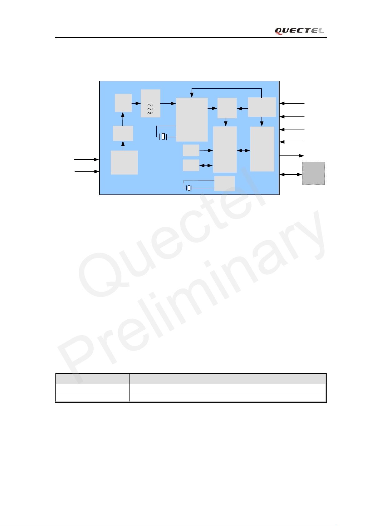
RF Front-
E
nd With
Integrated L
NA
Fractional-N
Synthesizer
GPS
Engine
ROM
Saw
Filter
Power
Management
ARM7
Processor
Peripheral
Controller
RTC
VCC
VIO/RTC
UART/I2C
RESET
EINT0
1PPS
ON/OFF
Optional
EEPROM
For CGEE
DR_I2C
Match
Network
RAM
LNA
PATCH
ANTENNA
Protocol
Type
NMEA
Input/output, ASCII, 0183, 3.01
OSP
Input/output, OSP protocol
Quectel
Preliminary
2.2 Functional Diagram
The block diagram of L50 is shown in the Figure 1.
Figure 1: Functional diagram for L50
2.3 Evaluation Board
In order to help customers to develop applications with L50, Quectel offers an Evaluation Board (EVB)
with appropriate power supply, RS-232 serial port and EEPROM.
Note: For more details, please refer to the document [1].
2.4 Protocol
L50 supports standard NMEA-0183 protocol and the One Socket Protocol (OSP), which is the binary
protocol interface that enables customers’ host device to access all SiRF GPS chip products of the
SiRF Star IV family and beyond. The module is capable of supporting the following NMEA formats:
GGA, GSA, GLL, GSV, RMC, and VTG..
Table 4: The module supports protocols
Note: Please refer to document [2] about NMEA standard protocol and SiRF private protocol.
L50_HD_V1.0 -11-
 Loading...