


BC660K-GL
Hardware Design
NB-IoT Module Series
Version: 1.0.0
Date: 2020-11-20
Status: Preliminary
www.quectel.com
NB-IoT Module Series
BC660K-GL Hardware Design
Our aim is to provide customers with timely and comprehensive service. For any assistance,
please contact our company headquarters:
Quectel Wireless Solutions Co., Ltd.
Building 5, Shanghai Business Park Phase III (Area B), No.1016 Tianlin Road, Minhang District, Shanghai
200233, China
Tel: +86 21 5108 6236
Email: info@quectel.com
Or our local office. For more information, please visit:
http://www.quectel.com/support/sales.htm.
For technical support, or to report documentation errors, please visit:
http://www.quectel.com/support/technical.htm
Or email to support@quectel.com.
General Notes
Quectel offers the information as a service to its customers. The information provided is based upon
customers’ requirements. Quectel makes every effort to ensure the quality of the information it makes
available. Quectel does not make any warranty as to the information contained herein, and does not
accept any liability for any injury, loss or damage of any kind incurred by use of or reliance upon the
information. All information supplied herein is subject to change without prior notice.
Disclaimer
While Quectel has made efforts to ensure that the functions and features under development are free from
errors, it is possible that these functions and features could contain errors, inaccuracies and omissions.
Unless otherwise provided by valid agreement, Quectel makes no warranties of any kind, implied or
express, with respect to the use of features and functions under development. To the maximum extent
permitted by law, Quectel excludes all liability for any loss or damage suffered in connection with the use of
the functions and features under development, regardless of whether such loss or damage may have been
foreseeable.
Duty of Confidentiality
The Receiving Party shall keep confidential all documentation and information provided by Quectel, except
when the specific permission has been granted by Quectel. The Receiving Party shall not access or use
Quectel’s documentation and information for any purpose except as expressly provided herein.
Furthermore, the Receiving Party shall not disclose any of the Quectel's documentation and information to
any third party without the prior written consent by Quectel. For any noncompliance to the above
requirements, unauthorized use, or other illegal or malicious use of the documentation and information,
Quectel will reserve the right to take legal action.
BC660K-GL_Hardware_Design
1
/ 59

NB-IoT Module Series
BC660K-GL Hardware Design
Copyright
The information contained here is proprietary technical information of Quectel wireless solutions co., ltd.
Transmitting, reproducing, disseminating and editing this document as well as using the content without
permission are forbidden. Offenders will be held liable for payment of damages. All rights are reserved in
the event of a patent grant or registration of a utility model or design.
Copyright © Quectel Wireless Solutions Co., Ltd. 2020. All rights reserved.
BC660K-GL_Hardware_Design
2
/ 59
About the Document
Version
Date
Author
Description
-
2020-09-30
Clifton HE/
Ellison WANG/
Randy LI
Creation of the document
1.0.0
2020-11-20
Clifton HE/
Ellison WANG/
Randy LI
Preliminary
Revision History
NB-IoT Module Series
BC660K-GL Hardware Design
BC660K-GL_Hardware_Design
3
/ 59

NB-IoT Module Series
BC660K-GL Hardware Design
Contents
About the Document.................................................................................................................................................3
Contents....................................................................................................................................................................... 4
Table Index.................................................................................................................................................................. 6
Figure Index.................................................................................................................................................................7
1 Introduction......................................................................................................................................................... 8
1.1. Safety Information....................................................................................................................................9
2 Product Concept..............................................................................................................................................10
2.1. General Description...............................................................................................................................10
2.2. Key Features.......................................................................................................................................... 11
2.3. Functional Diagram............................................................................................................................... 12
2.4. Evaluation Board....................................................................................................................................13
3 Application Interfaces.................................................................................................................................... 14
3.1. Pin Assignment...................................................................................................................................... 15
3.2. Pin Description.......................................................................................................................................16
3.3. Operating Modes................................................................................................................................... 20
3.4. Power Saving......................................................................................................................................... 21
3.4.1. Light Sleep..................................................................................................................................21
3.4.2. Deep Sleep.................................................................................................................................21
3.5. Power Supply......................................................................................................................................... 22
3.5.1. Power Supply Pins....................................................................................................................22
3.5.2. Reference Design for Power Supply......................................................................................23
3.5.3. Power Supply Voltage Detection*.......................................................................................... 23
3.6. Power-up/Power-down Scenarios...................................................................................................... 24
3.6.1. Power-up.................................................................................................................................... 24
3.6.2. Power-down............................................................................................................................... 25
3.6.3. Reset........................................................................................................................................... 25
3.6.4. Download....................................................................................................................................26
3.7. UART Interfaces.................................................................................................................................... 27
3.7.1. Main UART Port........................................................................................................................ 28
3.7.2. Debug UART Port..................................................................................................................... 28
3.7.3. UART Application......................................................................................................................29
3.8. (U)SIM Interface.....................................................................................................................................31
3.9. ADC Interface*....................................................................................................................................... 33
3.10. RI Interface*............................................................................................................................................33
3.11. NETLIGHT Interface*............................................................................................................................34
4 Antenna Interface............................................................................................................................................ 36
4.1. Pin Definition.......................................................................................................................................... 36
4.2. Operating Frequencies......................................................................................................................... 36
4.3. RF Antenna Reference Design........................................................................................................... 37
BC660K-GL_Hardware_Design
4
/ 59

NB-IoT Module Series
BC660K-GL Hardware Design
4.4. Reference Design of RF Layout..........................................................................................................38
4.5. Antenna Requirements.........................................................................................................................40
4.6. RF Output Power...................................................................................................................................41
4.7. RF Receiving Sensitivity.......................................................................................................................42
4.8. Recommended RF Connector for Antenna Installation.................................................................. 43
5 Reliability and Electrical Characteristics..................................................................................................45
5.1. Operating and Storage Temperatures............................................................................................... 45
5.2. Current Consumption............................................................................................................................46
5.3. Electrostatic Discharge.........................................................................................................................48
6 Mechanical Features.......................................................................................................................................49
6.1. Mechanical Dimensions........................................................................................................................49
6.2. Recommended Footprint......................................................................................................................51
6.3. Top and Bottom Views..........................................................................................................................52
7 Storage, Manufacturing and Packaging....................................................................................................53
7.1. Storage.................................................................................................................................................... 53
7.2. Manufacturing and Soldering...............................................................................................................54
7.3. Tape and Reel Packaging....................................................................................................................55
8 Appendix A References.................................................................................................................................57
BC660K-GL_Hardware_Design
5
/ 59

NB-IoT Module Series
BC660K-GL Hardware Design
Table Index
Table 1: Frequency Bands of BC660K-GL............................................................................................................10
Table 2: BC660K-GL Key Features........................................................................................................................11
Table 3: I/O Parameters Definition......................................................................................................................... 16
Table 4: Pin Description........................................................................................................................................... 16
Table 5: AP Operating Modes................................................................................................................................. 20
Table 6: Modem Operating Modes.........................................................................................................................20
Table 7: Module Operating Modes......................................................................................................................... 20
Table 8: Power Supply Pins.....................................................................................................................................23
Table 9: Reset Pin Definition................................................................................................................................... 25
Table 10: Pin Definition of UART Interfaces......................................................................................................... 27
Table 11: Pin Definition of (U)SIM Interface......................................................................................................... 31
Table 12: Pin Definition of ADC Interface..............................................................................................................33
Table 13: RI Signal Status....................................................................................................................................... 33
Table 14: Pin Definition of NB-IoT Antenna Interface.........................................................................................36
Table 15: Module Operating Frequencies.............................................................................................................36
Table 16: Antenna Cable Insertion Loss Requirements.....................................................................................40
Table 17: Required Antenna Parameters..............................................................................................................40
Table 18: RF Conducted Output Power................................................................................................................ 41
Table 19: Receiving Sensitivity (with RF Retransmissions)...............................................................................42
Table 20: Operation and Storage Temperatures................................................................................................. 45
Table 21: Module Current Consumption (3.3 V VBAT Power Supply).............................................................46
Table 22: Electrostatic Discharge Characteristics (25 ºC, 45 % Relative Humidity)..................................... 48
Table 23: Recommended Thermal Profile Parameters...................................................................................... 55
Table 24: Related Documents.................................................................................................................................57
Table 25: Terms and Abbreviations....................................................................................................................... 57
BC660K-GL_Hardware_Design
6
/ 59

NB-IoT Module Series
BC660K-GL Hardware Design
Figure Index
Figure 1: Functional Diagram.................................................................................................................................. 13
Figure 2: Pin Assignment......................................................................................................................................... 15
Figure 3: Module Power Consumption in Different Modes (Modem)............................................................... 21
Figure 4: Timing of Waking up Module from PSM............................................................................................... 22
Figure 5: Reference Circuit for Power Supply...................................................................................................... 23
Figure 6: Power-up Timing.......................................................................................................................................24
Figure 7: Power-down Timing..................................................................................................................................25
Figure 8: Reference Circuit of RESET_N by Using Driving Circuit...................................................................25
Figure 9: Reference Circuit of RESET_N by Using Button................................................................................ 26
Figure 10: Reference Circuit of BOOT by Using Button.....................................................................................27
Figure 11: Reference Design for Main UART Port.............................................................................................. 28
Figure 12: Reference Design of Debug UART Port............................................................................................ 28
Figure 13: Reference Circuit Design of UART..................................................................................................... 29
Figure 14: Sketch Map for RS-232 Interface Match............................................................................................30
Figure 15: Reference Circuit with Transistor Circuit............................................................................................31
Figure 16: Reference Circuit for (U)SIM Interface with a 6-pin (U)SIM Card Connector..............................32
Figure 17: RI Behaviour When a URC is Received.............................................................................................34
Figure 18: Reference Design of NETLIGHT.........................................................................................................35
Figure 19: Reference Design of NB-IoT Antenna Interface............................................................................... 38
Figure 20: Microstrip Design on a 2-layer PCB....................................................................................................38
Figure 21: Coplanar Waveguide Design on a 2-layer PCB................................................................................39
Figure 22: Coplanar Waveguide Design on a 4-layer PCB (Layer 3 as Reference Ground).......................39
Figure 23: Coplanar Waveguide Design on a 4-layer PCB (Layer 4 as Reference Ground).......................39
Figure 24: Dimensions of the U.FL-R-SMT Connector (Unit: mm)...................................................................43
Figure 25: Mechanicals of U.FL-LP Connectors.................................................................................................. 43
Figure 26: Space Factor of Mated Connector (Unit: mm).................................................................................. 44
Figure 27: BC660K-GL Top and Side Dimensions (Unit: mm)..........................................................................49
Figure 28: Module Bottom Dimension (Bottom View).........................................................................................50
Figure 29: Recommended Footprint (Unit: mm)...................................................................................................51
Figure 30: Top View of the Module.........................................................................................................................52
Figure 31: Bottom View of the Module...................................................................................................................52
Figure 32: Recommended Reflow Soldering Thermal Profile........................................................................... 54
Figure 33: Tape Dimensions (Unit: mm)................................................................................................................56
Figure 34: Reel Dimensions (Unit: mm)................................................................................................................ 56
BC660K-GL_Hardware_Design
7
/ 59

NB-IoT Module Series
BC660K-GL Hardware Design
1 Introduction
This document defines the BC660K-GL module and describes its air interfaces and hardware interface
which are connected with the customers’ applications.
This document helps customers quickly understand the interface specifications, electrical and mechanical
details, as well as other related information of the module. To facilitate application designs, it also
includes some reference designs for customers’ reference. The document, coupled with application notes
and user guides, makes it easy to design and set up mobile applications with BC660K-GL.
BC660K-GL_Hardware_Design
1-8
/ 59
NB-IoT Module Series
Full attention must be paid to driving at all times in order to reduce the risk of an
accident. Using a mobile while driving (even with a handsfree kit) causes
distraction and can lead to an accident. Please comply with laws and regulations
restricting the use of wireless devices while driving.
Switch off the cellular terminal or mobile before boarding an aircraft. The operation
of wireless appliances in an aircraft is forbidden to prevent interference with
communication systems. If there is an Airplane Mode, it should be enabled prior to
boarding an aircraft. Please consult the airline staff for more restrictions on the use
of wireless devices on an aircraft.
Wireless devices may cause interference on sensitive medical equipment, so
please be aware of the restrictions on the use of wireless devices when in
hospitals, clinics or other healthcare facilities.
Cellular terminals or mobiles operating over radio signals and cellular network
cannot be guaranteed to connect in all possible conditions (for example, with
unpaid bills or with an invalid (U)SIM card). When emergency help is needed in
such conditions, please remember using emergency call. In order to make or
receive a call, the cellular terminal or mobile must be switched on in a service area
with adequate cellular signal strength.
The cellular terminal or mobile contains a transmitter and receiver. When it is ON, it
receives and transmits radio frequency signals. RF interference can occur if it is
used close to TV set, radio, computer or other electric equipment.
In locations with potentially explosive atmospheres, obey all posted signs to turn
off wireless devices such as mobile phone or other cellular terminals. Areas with
potentially explosive atmospheres include fuelling areas, below decks on boats,
fuel or chemical transfer or storage facilities, areas where the air contains
chemicals or particles such as grain, dust or metal powders, etc.
BC660K-GL Hardware Design
1.1. Safety Information
The following safety precautions must be observed during all phases of operation, such as usage, service
or repair of any cellular terminal or mobile incorporating the module. Manufacturers of the cellular terminal
should notify users and operating personnel of the following safety information by incorporating these
guidelines into all manuals of the product. Otherwise, Quectel assumes no liability for customers’ failure to
comply with these precautions.
BC660K-GL_Hardware_Design
1-9
/ 59
NB-IoT Module Series
“*” means under development.
Mode
BC660K-GL
H-FDD
B1/B2/B3/B4/B5/B8/B12/B13/B14/B17/B18/B19/B20/B25/B28/B66/B70/B85
NOTE
BC660K-GL Hardware Design
2 Product Concept
2.1. General Description
BC660K-GL is a high-performance NB-IoT module with extremely low power consumption. It is designed
to communicate with infrastructures of mobile network operators through NB-IoT radio protocols (3GPP
Rel-13 and 3GPP Rel-14). BC660K-GL supports a broad range of frequency bands as listed below.
Table 1: Frequency Bands of BC660K-GL
BC660K-GL is an SMD type module with LCC and LGA package, and has an ultra-compact profile of
17.7 mm × 15.8 mm × 2.0 mm, which makes it easily embedded into size-constrained applications and
provide reliable connectivity with the applications.
BC660K-GL provides abundant external interfaces (UART, ADC, (U)SIM, etc) and protocol stacks
(UDP/TCP/LwM2M*/MQTT*, etc.), which provide great convenience for customers' applications.
Due to compact form factor, ultra-low power consumption and extended temperature range, BC660K-GL
is a best choice for a wide range of IoT applications, such as smart metering, bike sharing, smart
wearables, smart parking, smart city, home appliances, security and asset tracking, agricultural and
environmental monitoring, etc. It is able to provide a complete range of SMS* and data transmission
services to meet customers’ demands.
The module fully complies with the RoHS directive of the European Union.
BC660K-GL_Hardware_Design
2-10
/ 59
BC660K-GL Hardware Design
Feature
Details
Power Supply
Supply voltage: 2.2–4.3 V
Typical supply voltage: 3.3 V
Power Saving
Typical power consumption: 800 nA
Frequency Bands
LTE Cat NB2:
B1/B2/B3/B4/B5/B8/B12/B13/B14/B17/B18/B19/B20/B25/B28/B66/B70/
B85
Transmitting Power
23 dBm ±2 dB
(U)SIM Interface
Support 1.8/3.0 V (U)SIM card
UART Interfaces
Main UART Port:
Used for AT command communication and data transmission, the baud
rate is 115200 bps by default. For more details, see Chapter 3.7.1.
Used for firmware upgrade, and in such case, the baud rate is 921600
bps by default.
Debug UART Port:
Used for firmware debugging
Default baud rate: 6 Mbps
Network Protocols
UDP/TCP/SNTP/LwM2M*/MQTT*/TLS*/DTLS*
SMS*Text/PDU Mode
Data Transmission
Features
Single-tone (max): 25.5 kbps (DL)/16.7 kbps (UL)
Multi-tone (max): 127 kbps (DL)/158.5 kbps (UL)
AT Commands
3GPP TS 27.005/3GPP TS 27.007 AT commands (3GPP Rel-13 and
3GPP Rel-14) and Quectel enhanced AT commands
Firmware Update
Upgrade firmware via main UART port
Upgrade firmware via DFOTA
Real Time Clock
Supported
Physical Characteristics
Size: (17.7 ±0.15) mm × (15.8 ±0.15) mm × (2.0 ±0.2) mm
Weight: 1.0 ±0.2 g
Temperature Range
Operating temperature range: -35 to +75 °C
1)
Extended temperature range: -40 to +85 °C
2)
Storage temperature range: -40 to +90 °C
2.2. Key Features
The following table describes the detailed features of BC660K-GL module.
Table 2: BC660K-GL Key Features
NB-IoT Module Series
BC660K-GL_Hardware_Design
2-11
/ 59
NB-IoT Module Series
1.
1)
Within operating temperature range, the module is 3GPP compliant.
2.
2)
Within extended temperature range, the module remains the ability to establish and maintain
functions such as SMS* and data transmission, without any unrecoverable malfunction. Radio
spectrum and radio network will not be influenced, while one or more specifications, such as Pout,
may exceed the specified tolerances of 3GPP. When the temperature returns to the normal operation
temperature levels, the module will meet 3GPP specifications again.
3. "*" means under development.
Antenna Interface
50 Ω impedance control
RoHS
All hardware components are fully compliant with EU RoHS directive
NOTES
BC660K-GL Hardware Design
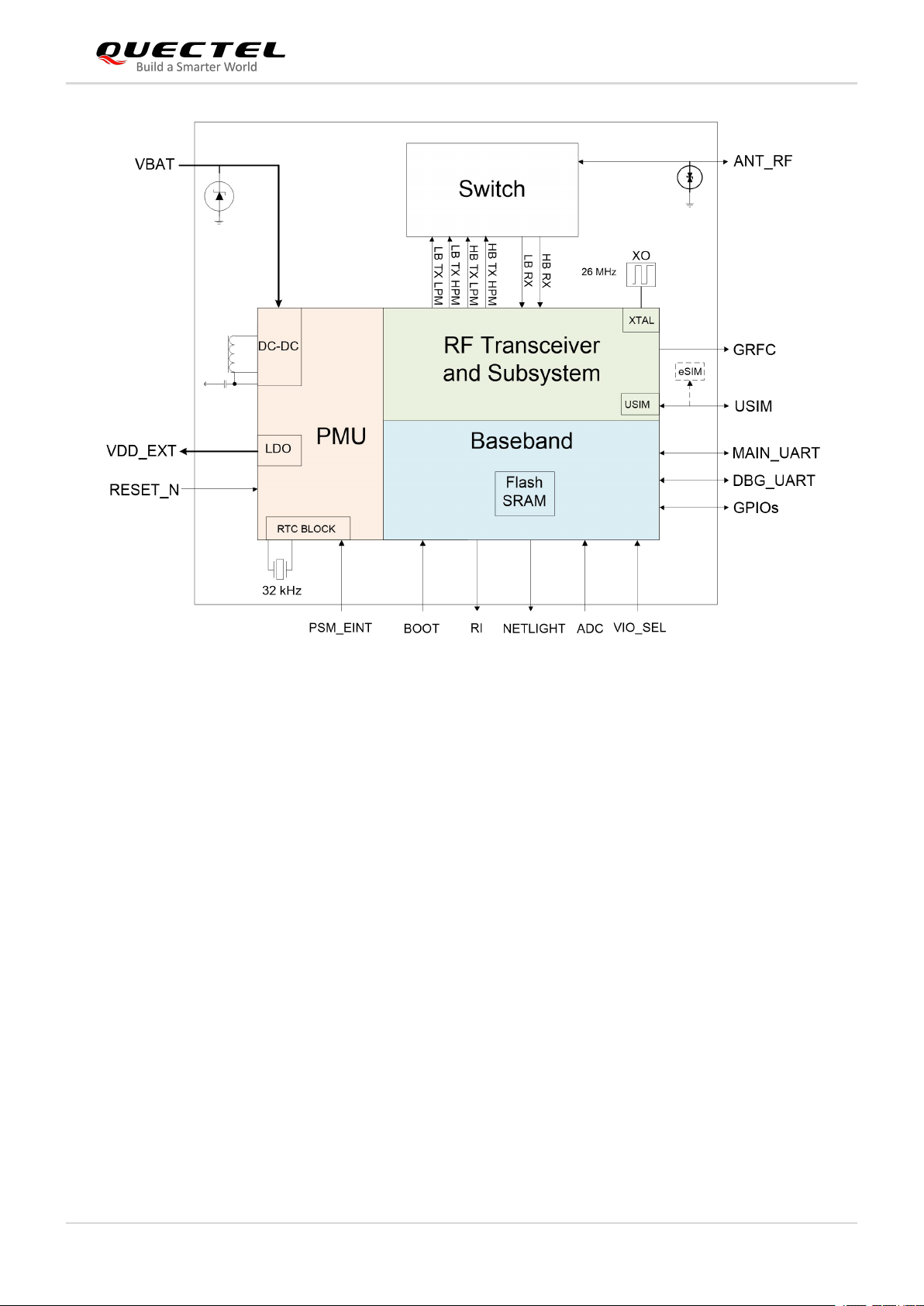
2.3. Functional Diagram
The following figure shows a block diagram of BC660K-GL and illustrates the major functional parts.
Radio frequency
Baseband
Power management
Peripheral interfaces
BC660K-GL_Hardware_Design
2-12
/ 59
NB-IoT Module Series
BC660K-GL Hardware Design
Figure 1: Functional Diagram
2.4. Evaluation Board
Quectel provides a complete set of development tools to facilitate the use and testing of BC660K-GL
module. The development tool kit includes the TE-B board, a USB cable, an antenna and other
peripherals. For more details, see document [1].
BC660K-GL_Hardware_Design
2-13
/ 59
NB-IoT Module Series
"*" means under development.
NOTE
BC660K-GL Hardware Design
3 Application Interfaces
BC660K-GL is equipped with a total of 58 pins, including 44 LCC pins and 14 LGA pins. The subsequent
chapters will provide detailed descriptions of the following functions/pins/interfaces:
Power Supply
PSM_EINT
RESET_N
BOOT
UART Interfaces
(U)SIM Interface
ADC Interface*
RI Interface*
NETLIGHT Interface*
BC660K-GL_Hardware_Design
3-14
/ 59
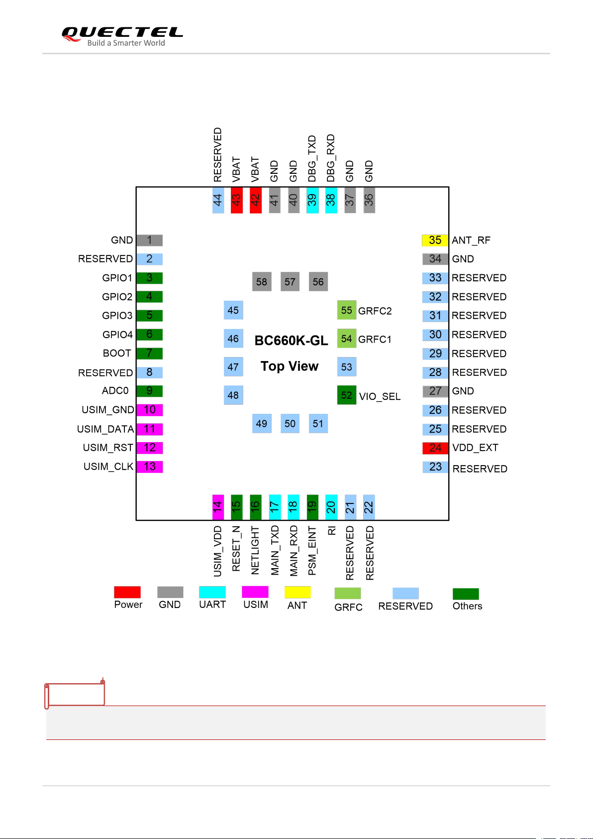
3.1. Pin Assignment
Keep all reserved and unused pins unconnected.
NOTE
NB-IoT Module Series
BC660K-GL Hardware Design
BC660K-GL_Hardware_Design
Figure 2: Pin Assignment
3-15
/ 59
3.2. Pin Description
Type
Description
AI
Analog input
AO
Analog output
DI
Digital input
DO
Digital output
IO
Bidirectional
PI
Power input
PO
Power output
Power Supply
Pin Name
Pin No.
I/O
Description
DC Characteristics
Comment
VBAT
42, 43
PI
Power supply for
the module
Vmax = 4.3 V
Vmin = 2.2 V
Vnorm = 3.3 V
VDD_EXT
24
PO
1.8/3.3 V output
for external
circuit
Vnorm = 1.8/3.3 V
No voltage output in
Deep Sleep/Light
Sleep mode.
It is intended to supply
power for the module’s
pull-up circuits, and is
not recommended to
be used as the power
supply for external
circuits.
GND
1, 27, 34, 36, 37, 40, 41, 56, 57, 58
Power Key Interface
Pin Name
Pin No.
I/O
Description
DC Characteristics
Comment
Table 3: I/O Parameters Definition
NB-IoT Module Series
BC660K-GL Hardware Design
Table 4: Pin Description
BC660K-GL_Hardware_Design
3-16
/ 59
NB-IoT Module Series
BOOT
7
DI
Control module
enter download
mode
VILmax = 0.2 × VDD_EXT
VIHmin = 0.7 × VDD_EXT
Active low.
Reset Interface
Pin Name
Pin No.
I/O
Description
DC Characteristics
Comment
RESET_N
15
DI
Reset the
module
VILmax = 0.38 V
VIHmin = 1.33 V
VIHmax = 3.6 V
Active low.
PSM_EINT Interface
Pin Name
Pin No.
I/O
Description
DC Characteristics
Comment
PSM_EINT
19
DI
Dedicated
external interrupt
pin used to wake
up the module
from Deep
Sleep/Light
Sleep mode..
VILmax = 0.38 V
VIHmin = 1.33 V
VIHmax = 3.6 V
Active on falling
edge.
Network Status Indication*
Pin Name
Pin No.
I/O
Description
DC Characteristics
Comment
NETLIGHT
16
DO
Indicate the
module's
network activity
status
VOLmax = 0.15 × VDD_EXT
VOHmin = 0.8 × VDD_EXT
ADC Interface*
Pin Name
Pin No.
I/O
Description
DC Characteristics
Comment
ADC0
9
AI
General-purpose
analog to digital
converter
interface
Voltage range:
0–1.2 V
Main UART Port
Pin Name
Pin No.
I/O
Description
DC Characteristics
Comment
MAIN_RXD
18
DI
Main UART
receive
VILmax = 0.2×VDD_EXT
VIHmin = 0.7×VDD_EXT
MAIN_TXD
17
DO
Main UART
transmit
VOLmax = 0.15 × VDD_EXT
VOHmin = 0.8 × VDD_EXT
VDD_EXT
power domain.
BC660K-GL Hardware Design
BC660K-GL_Hardware_Design
3-17
/ 59
NB-IoT Module Series
Debug UART Port
Pin Name
Pin No.
I/O
Description
DC Characteristics
Comment
DBG_RXD
38
DI
Debug UART
receive
VILmax = 0.2 × VDD_EXT
VIHmin = 0.7 × VDD_EXT
VDD_EXT
power domain.
DBG_TXD
39
DO
Debug UART
transmit
VOLmax = 0.15×VDD_EXT
VOHmin = 0.8×VDD_EXT
Ringing Signal*
Pin Name
Pin No.
I/O
Description
DC Characteristics
Comment
RI20DO
Ring indication
VOLmax = 0.15×VDD_EXT
VOHmin = 0.8×VDD_EXT
VDD_EXT
power domain.
(U)SIM Interface
Pin Name
Pin No.
I/O
Description
DC Characteristics
Comment
(U)SIM_VDD
14
DO
(U)SIM card
power supply
Vnorm = 1.8/3.0 V
(U)SIM_RST
12
DO
(U)SIM card
reset
VOLmax = 0.15 × (U)SIM_VDD
VOHmin = 0.8 × (U)SIM_VDD
(U)SIM_DAT
A
11
IO
(U)SIM card
data
VILmax = 0.2 × (U)SIM_VDD
VIHmin = 0.7 × (U)SIM_VDD
VOLmax = 0.15 × (U)SIM_VDD
VOHmin = 0.8 ×(U)SIM_VDD
(U)SIM_CLK
13
DO
(U)SIM card
clock
VOLmax = 0.15 × (U)SIM_VDD
VOHmin = 0.8 × (U)SIM_VDD
(U)SIM_GND
10
Specified
ground for
(U)SIM card
Antenna Interface
Pin Name
Pin No.
I/O
Description
DC Characteristics
Comment
ANT_RF
35
IO
RF antenna
interface
50 Ω
characteristic
impedance
GPIO Interfaces
Pin Name
Pin No.
I/O
Description
DC Characteristics
Comment
GPIO1
3
IO
General-purpose
input/output
VILmax = 0.2×VDD_EXT
VIHmin = 0.7×VDD_EXT
VOLmax = 0.15×VDD_EXT
VOHmin = 0.8 × VDD_EXT
VDD_EXT
power domain.
GPIO2
4
IO
General-purpose
input/output
BC660K-GL Hardware Design
BC660K-GL_Hardware_Design
3-18
/ 59
NB-IoT Module Series
1. Keep all reserved and unused pins unconnected.
2. When VIO_SEL is grounded and VBAT ˂ 3.3 V, VDD_EXT = VBAT;
When VIO_SEL is grounded and VBAT ≥ 3.3 V, VDD_EXT = 3.3 V;
When VIO_SEL is floating, VDD_EXT = 1.8 V.
3. “*” means under development.
If unused, keep
these pins open.
GPIO3
5
IO
General-purpose
input/output
GPIO4
6
IO
General-purpose
input/output
GRFC Interfaces
Pin Name
Pin No.
I/O
Description
DC Characteristics
Comment
GRFC1
54
DO
Generic RF
controller
1.8 V power
domain.
If unused, keep
these pins open.
GRFC2
55
DO
Generic RF
controller
Other Interface Pin
Pin Name
Pin No.
I/O
Description
DC Characteristics
Comment
VIO_SEL
52
DI
IO Voltage
selection
Floating: 1.8 V
0: 3.3 V
Control
VDD_EXT
voltage select
1.8 V or 3.3 V
Reserved Pins
Pin Name
Pin No.
I/O
Description
DC Characteristics
Comment
RESERVED
2, 8, 21–23, 25, 26, 28–33, 44–51, 53
Keep these pins
open.
NOTES
BC660K-GL Hardware Design
BC660K-GL_Hardware_Design
3-19
/ 59
BC660K-GL Hardware Design
Mode
Description
Normal
In normal mode, the AP handles tasks, such as AT command communication.
Idle
When all tasks are suspended, the AP will enter idle mode.
Mode
Description
Connected
The network is connected and the module supports data transmission. In such a case,
the modem can switch to DRX/eDRX mode.
DRX/eDRX
The modem is in idle mode, and downlink data can be received during PTW only. In
such a case, the modem can switch to PSM or connected mode.
PSM
In power saving mode, the modem is disconnected from the network and cannot
receive any downlink data. In such a case, the modem can switch to eDRX/DRX.
Mode
Description
Active
When the AP is in normal mode or the modem is in connected mode, the module will be
active and supports all services and functions.
The current consumption in active mode is higher than that in sleep modes.
Light Sleep
Generally, when the AP is in idle mode and the modem is in DRX/eDRX mode, the
module will enter Light Sleep mode. In such a case, the AP tasks will be suspended and
the modem will be able to receive downlink data during PTW only.
In Light Sleep mode, the current consumption of the module is reduced greatly.
Deep Sleep
When the AP is in idle mode and the modem is idle or inactive, the module will enter
deep sleep mode in which the CPU is powered off and only the 32 kHz RTC clock is
working.
In deep sleep mode, the current consumption will be reduced to the minimum (typical
value: 800 nA).
3.3. Operating Modes
The following table describes the three working modes of the module briefly.
Table 5: AP Operating Modes
NB-IoT Module Series
Table 6: Modem Operating Modes
Table 7: Module Operating Modes
BC660K-GL_Hardware_Design
3-20
/ 59

NB-IoT Module Series
BC660K-GL Hardware Design
3.4. Power Saving
Upon system requirement, there are several ways to drive the module to enter low current consumption
status.
3.4.1. Light Sleep
In Light Sleep mode, the serial port does not work, and the module can be woken up through the falling
edge of PSM_EINT.
In this mode, the UART port is inactive and the module can be awakened through the main UART port.
3.4.2. Deep Sleep
The module consumes extremely low current in Deep Sleep mode (typical value: 800 nA). The main
purpose of Deep Sleep is to reduce the power consumption of the module and prolong the power supply
time of the battery.
In Deep Sleep mode, the serial port does not work. The following figure shows the power consumption
diagram of the module in different modes.
Figure 3: Module Power Consumption in Different Modes (Modem)
BC660K-GL_Hardware_Design
3-21
/ 59

NB-IoT Module Series
BC660K-GL Hardware Design
When the modem remains in PSM and the AP is in idle mode, the module will enter deep sleep mode.
The procedure of the modem entering PSM is as follows:
The modem requests to enable PSM in ATTACH REQUEST or TAU REQUEST message during
ATTACH/TAU (Tracking Area Update) procedure. Then the network accepts the request and provides an
active time value (T3324) to the modem and the mobile reachable timer starts. When the T3324 timer
expires, the modem enters PSM for the duration of T3412 (periodic TAU timer). Please note that the
module cannot request entering PSM when it is establishing an emergency attachment or initializing the
PDN (Public Data Network) connection
When the module is in deep sleep mode, it will be woken up in the following cases:
After the T3412 timer expires, the module will exit deep sleep automatically.
Send an AT command to the module (this AT command will be lost), pull down the MAIN_RXD, and
in falling edge, the module will be woken up from deep sleep.
Pulling down PSM_EINT (falling edge) will wake up the module from deep sleep.
The timing of waking up the module from PSM is illustrated below.
Figure 4: Timing of Waking up Module from PSM
3.5. Power Supply
3.5.1. Power Supply Pins
The module provides two VBAT pins for connection with an external power supply. The table below
describes the module's VBAT and ground pins.
BC660K-GL_Hardware_Design
3-22
/ 59

NB-IoT Module Series
Pin Name
Pin No.
Description
Min.
Typ.
Max.
Unit
VBAT
42, 43
Power supply for the
module
2.2
3.3
4.3
V
GND
1, 27, 34, 36,
37, 40, 41, 56,
57, 58
GND
BC660K-GL Hardware Design
Table 8: Power Supply Pins
3.5.2. Reference Design for Power Supply
Power design for a module is critical to its performance. It is recommended to use a low quiescent current
LDO with output current capacity of 0.5 A as the power supply for BC660K-GL.
(Li-SOCl2) batteries and Lithium manganese oxide (LiMn2O4) batteries
supply. The supply voltage of the module ranges from 2.2 V to 4.3 V. When the module is working, ensure
its input voltage will never drop below 2.2 V; otherwise the module will be abnormal.
can also be used as the power
Lithium-thionyl chloride
For better power performance, it is recommended to place a 100 μF tantalum capacitor with low ESR
(ESR = 0.7 Ω) and three ceramic capacitors (100 nF, 100 pF and 22 pF) near the VBAT pins. Also, it is
recommended to add a TVS diode on the VBAT trace (near VBAT pins) to improve surge voltage
withstand capability. In principle, the longer the VBAT trace is, the wider it should be. A reference circuit
for power supply is illustrated in the following figure.
3.5.3. Power Supply Voltage Detection*
You can use AT+CBC to monitor and query the current VBAT voltage. The unit of the voltage value is
millivolt. For detailed information about the command, see document [2].
BC660K-GL_Hardware_Design
Figure 5: Reference Circuit for Power Supply
3-23
/ 59

NB-IoT Module Series
“*” means under development.
1. After the VBAT is powered down, its voltage must be lower than 0.7 V. The specific discharge time
needs to be evaluated based on the actual circuit test, and enough margin is left to avoid abnormal
startup when the it is powered on again.
2. The power-up time of VBAT must be within 10 ms.
3. It is recommended that the MCU retain the RESET_N control pin. When the abnormal power-on
sequence causes the module to start abnormally, the RESET_N control pin can control the module to
reset to exit the abnormal state.
4. After VBAT is powered on, RESET_N and BOOT automatically rise to high level due to internal
pull-ups.
NOTES
NOTE
BC660K-GL Hardware Design
3.6. Power-up/Power-down Scenarios
3.6.1. Power-up
After the module VBAT is powered on, keep the RESET_N and BOOT inputs not being pulled down, and
the module can turn on automatically. The power-up timing is illustrated in the following figure.
Figure 6: Power-up Timing
BC660K-GL_Hardware_Design
3-24
/ 59

3.6.2. Power-down
Pin Name
Pin No.
Description
Reset Pull-down Time
RESET_N
15
Reset the module.
Active low.
≥
50 ms
The module can be shut down through disconnecting VBAT power supply.
Figure 7: Power-down Timing
NB-IoT Module Series
BC660K-GL Hardware Design
3.6.3. Reset
Driving RESET_N low for at least 50 ms will reset the module.
Table 9: Reset Pin Definition
The recommended circuits of resetting the module are shown below. An open drain/collector driver or
button can be used to control the RESET_N pin.
BC660K-GL_Hardware_Design
Figure 8: Reference Circuit of RESET_N by Using Driving Circuit
3-25
/ 59

NB-IoT Module Series
1. When the high level output of RESET_CONTROL is more than 1.7 V and less than 3.6 V, and the low
level output is less than 0.35 V, it is recommended to use the direct connection method to control the
RESET_N pin of the module. In other cases, it must be controlled by an open collector drive circuit.
2. It is recommended to reserve a 100 nF capacitor position, which is not mounted by default.
NOTES
BC660K-GL Hardware Design
Figure 9: Reference Circuit of RESET_N by Using Button
3.6.4. Download
In the process of system reset or power-on, keep the BOOT pin input low and the module will enter the
download mode.
In download mode, the firmware can be downloaded through the main serial port. After the download is
complete, the module needs to be reset to exit the download mode.
An open drain/collector driver or button can be used to control the BOOT pin.
BC660K-GL_Hardware_Design
3-26
/ 59

NB-IoT Module Series
If the BOOT pin is connected to a filter capacitor in parallel, the capacitance of the capacitor cannot be
higher than 33 pF.
Interface
Pin Name
Pin No.
Description
Main UART Port
MAIN_TXD
17
Main UART transmit
MAIN_RXD
18
Main UART receive
Debug UART Port
DBG_RXD
38
Debug UART receive
DBG_TXD
39
Debug UART transmit
Ring Indication
RI*
20
Ring indication (when there is a SMS or a URC
output, the module will inform DTE with the RI pin)
NOTE
BC660K-GL Hardware Design
Figure 10: Reference Circuit of BOOT by Using Button
3.7. UART Interfaces
The module provides two UART ports: main UART port and debug UART port. The module is designed
as DCE (Data Communication Equipment), following the traditional DCE-DTE (Data Terminal Equipment)
connection.
Table 10: Pin Definition of UART Interfaces
BC660K-GL_Hardware_Design
3-27
/ 59

NB-IoT Module Series
BC660K-GL Hardware Design
3.7.1. Main UART Port
The main UART port supports AT command communication, data transmission and firmware upgrade.
Default baud rate: 115200 bps
Fixed baud rates: 2400 bps, 4800 bps, 9600 bps, 19200 bps, 38400 bps, 57600 bps, 115200 bps,
230400 bps, 460800 bps
When the port is used for firmware upgrade, the baud rate is 921600 bps by default.
When the module enters Deep Sleep/Light Sleep mode, it can wake up the module by sending AT
commands through the main serial port. It is generally recommended to send the command AT
continuously until OK is returned before sending AT commands to other services.
The figure below shows the connection between DCE and DTE.
Figure 11: Reference Design for Main UART Port
3.7.2. Debug UART Port
Through debug tools, the debug UART port can be used to output logs for firmware debugging. Its baud
rate is 6 Mbps by default. The following is a reference design of debug UART port.
Figure 12: Reference Design of Debug UART Port
BC660K-GL_Hardware_Design
3-28
/ 59

NB-IoT Module Series
BC660K-GL Hardware Design
3.7.3. UART Application
The serial port voltage domain of this module is optional. Customers can select the appropriate voltage
domain through VIO_SEL according to the actual situation. When VIO_SEL is floating, the VDD_EXT
voltage domain is 1.8 V; when VIO_SEL is grounded, the VDD_EXT voltage domain is 3.3 V.
If the voltage domain of the customer application system is 1.8 V, VIO_SEL can be floating; If the voltage
domain of the customer application system is 3.3 V, VIO_SEL can be grounded.
The following figure shows the reference circuit design:
Figure 13: Reference Circuit Design of UART
The following circuit shows a reference design for the communication between the module and a PC with
standard RS-232 interface. Make sure to select appropriate voltage domain through VIO_SEL according
to the actual situation.
BC660K-GL_Hardware_Design
3-29
/ 59

NB-IoT Module Series
1. If the voltage domain of your application system is 1.8 V, keep the R1 marked in red not mounted; If
the voltage domain of your application system is 3.3 V, keep the R1 marked in red mounted.
2. “ ” represents the test points of UART interfaces. It is also recommended to reserve the test points
of VBAT, BOOT and RESET_N, for convenient firmware upgrade and debugging when necessary.
3. VDD_EXT cannot pull up the module MAIN_RXD directly. If VDD_EXT need pull up the module
MAIN_RXD, you need to connect a Schottky diode in series first, and then pull up the module
MAIN_RXD through a 4.7-20 kΩ resistor. For more details, see document [3].
4. When VIO_SEL is grounded and VBAT ˂ 3.3 V, VDD_EXT = VBAT;
When VIO_SEL is grounded and VBAT ≥ 3.3 V, VDD_EXT = 3.3 V;
When VIO_SEL is floating, VDD_EXT = 1.8 V.
NOTES
BC660K-GL Hardware Design
Figure 14: Sketch Map for RS-232 Interface Match
Please visit vendors’ websites to select a suitable RS-232 transceiver, such as: http://www.exar.com and
http://www.maximintegrated.com.
When the serial port voltage is neither 1.8 V nor 3.3 V, it is recommended to use a transistor level
conversion circuit. The circuit design of dotted line section can refer to the design of solid line section, in
terms of both module input and output circuit designs, but please pay attention to the direction of
connection.
BC660K-GL_Hardware_Design
3-30
/ 59

BC660K-GL Hardware Design
1. VDD_EXT cannot pull up MAIN_RXD directly. Due to the anti-backflow design of the MAIN_RXD pin,
MAIN_RXD pin can be directly connected to the TXD of DTE in the 1.8–3.3 V voltage domain. If the
Deep Sleep/Light Sleep mode wake-up function of the MAIN_RXD is enabled, it is recommended
that MAIN_RXD does not use a level conversion circuit to avoid abnormal wake-up.
2. If you choose the transistor conversion circuit, don’t mount the R1 marked in red.
3. If VDD_EXT need pull up the module MAIN_RXD, you need to connect a Schottky diode in series
first, and then pull up the module MAIN_RXD through a 4.7-20 kΩ resistor. For more details, see
document [3].
4. Transistor circuit solution is not suitable for applications with high baud rates exceeding 460 kbps.
Pin Name
Pin
No.
Description
Comment
(U)SIM_VDD
14
(U)SIM card power supply
When 3.0 V ≤ VBAT ≤ 4.3 V, support
1.8/3.0 V (U)SIM card;
When 2.2 V ≤ VBAT < 3 V, only support
1.8 V (U)SIM card;
Maximum supply current: about 80 mA.
NOTES
Figure 15: Reference Circuit with Transistor Circuit
NB-IoT Module Series
3.8. (U)SIM Interface
The (U)SIM card is powered by an internal regulator in the module. Both 1.8 V and 3.0 V (U)SIM cards
are supported.
Table 11: Pin Definition of (U)SIM Interface
BC660K-GL_Hardware_Design
3-31
/ 59

NB-IoT Module Series
(U)SIM_CLK
13
(U)SIM card clock
(U)SIM_DATA
11
(U)SIM card data
(U)SIM_RST
12
(U)SIM card reset
(U)SIM_GND
10
Specified ground for (U)SIM card
BC660K-GL Hardware Design
A reference circuit design for (U)SIM interface with a 6-pin (U)SIM card connector is illustrated below.
Figure 16: Reference Circuit for (U)SIM Interface with a 6-pin (U)SIM Card Connector
To enhance the reliability and availability of the (U)SIM card in applications, follow the criteria below in
(U)SIM circuit design:
Keep the placement of (U)SIM card connector as close to the module as possible. Keep the trace
length as less than 200 mm as possible.
Keep (U)SIM card signals away from RF and VBAT traces.
Assure the trace between the ground of the module and that of (U)SIM card connector is short and
wide. Keep the trace width of the ground no less than 0.5 mm to maintain the same electric potential.
The decoupling capacitor between (U)SIM_VDD and GND should be not more than 1 μF and be
placed close to the (U)SIM card connector.
To avoid cross-talk between (U)SIM_DATA and (U)SIM_CLK, keep them away from each other and
shield them separately with the surrounded ground.
In order to offer good ESD protection, it is recommended to add a TVS diode array whose parasitic
capacitance should be not more than 50 pF. The ESD protection device should be placed as close to
(U)SIM card connector as possible, and ensure the (U)SIM card signal lines go through the ESD
protection device first from (U)SIM card connector and then to the module. The 22 Ω resistors should
be connected in series between the module and the (U)SIM card connector to suppress EMI spurious
transmission and enhance ESD protection. Please note that the (U)SIM peripheral circuit should be
BC660K-GL_Hardware_Design
3-32
/ 59

NB-IoT Module Series
It is necessary (U)SIM_DATA must add a 10 kΩ pull-up resistor to (U)SIM_VDD to improve
anti-interference ability.
1. 320 kΩ pull-down resistor is integrated inside the ADC pin. This resistor needs to be considered
when calculating the resistor divider relationship.
2. “*” means under development.
Pin Name
Pin No.
Description
Sample Range
ADC0
9
Analog to digital converter interface
0–1.2 V
Module Status
RI Signal Level
Standby
High pulse
URC
When a URC is received, RI outputs 120 ms low pulse and starts data output.
NOTES
NOTE
BC660K-GL Hardware Design
close to the (U)SIM card connector.
The pull-up resistor on the SIM_DATA line can improve anti-jamming capability and should be placed
close to the (U)SIM card connector.
3.9. ADC Interface*
The module provides a 12-bit ADC input channel to read the voltage value.
Table 12: Pin Definition of ADC Interface
3.10. RI Interface*
When there is a message received or a URC output, the module will notify DTE through the RI interface.
Table 13: RI Signal Status
BC660K-GL_Hardware_Design
3-33
/ 59

BC660K-GL Hardware Design
“*” means under development.
NOTE
Figure 17: RI Behaviour When a URC is Received
NB-IoT Module Series
3.11. NETLIGHT Interface*
NETLIGHT can be used to indicate the network status of the module. The following table illustrates the
module status indicated by NETLIGHT.
A reference circuit is shown as below.
BC660K-GL_Hardware_Design
3-34
/ 59

BC660K-GL Hardware Design
“*” means under development.
NOTE
Figure 18: Reference Design of NETLIGHT
NB-IoT Module Series
BC660K-GL_Hardware_Design
3-35
/ 59

BC660K-GL Hardware Design
Pin Name
Pin No.
Description
ANT_RF
35
RF antenna interface
GND
34, 36, 37
Ground
Frequency Band
Receiving Frequency
Transmitting Frequency
B1
2110–2170 MHz
1920–1980 MHz
B2
1930–1990 MHz
1850–1910 MHz
B3
1805–1880 MHz
1710–1785 MHz
B4
2110–2155 MHz
1710–1755 MHz
B5
869–894 MHz
824–849 MHz
B8
925–960 MHz
880–915 MHz
B12
729–746 MHz
699–716 MHz
B13
746–756 MHz
777–787 MHz
4 Antenna Interface
The pin 35 is the RF antenna pad. The antenna port has an impedance of 50 Ω.
4.1. Pin Definition
Table 14: Pin Definition of NB-IoT Antenna Interface
NB-IoT Module Series
4.2. Operating Frequencies
Table 15: Module Operating Frequencies
BC660K-GL_Hardware_Design
4-36
/ 59

NB-IoT Module Series
B14
758–768 MHz
788–798 MHz
B17
734–746 MHz
704–716 MHz
B18
860–875 MHz
815–830 MHz
B19
875–890 MHz
830–845 MHz
B20
791–821 MHz
832–862 MHz
B25
1930–1995 MHz
1850–1915 MHz
B28
758–803 MHz
703–748 MHz
B66
2110–2180 MHz
1710–1780 MHz
B70
1995–2020 MHz
1695–1710 MHz
B85
728–746 MHz
698–716 MHz
BC660K-GL Hardware Design
4.3. RF Antenna Reference Design
BC660K-GL provides an RF antenna pin for external NB-IoT antenna connection.
The RF trace on host PCB connected to the module’s RF antenna pad should be coplanar
waveguide or microstrip, whose characteristic impedance should be close to 50 Ω.
The module comes with ground pads which are next to the antenna pad to give a better grounding.
In order to achieve better RF performance, it is recommended to reserve a π type matching circuit
and place the π-type matching components (R1/C1/C2) as close to the antenna as possible. By
default, the capacitors (C1/C2) are not mounted and a 0 Ω resistor is mounted on R1.
A reference design of the RF interface is shown as below.
BC660K-GL_Hardware_Design
4-37
/ 59

Figure 19: Reference Design of NB-IoT Antenna Interface
4.4. Reference Design of RF Layout
NB-IoT Module Series
BC660K-GL Hardware Design
For users’ PCB, the characteristic impedance of all RF traces should be controlled to 50 Ω. The
impedance of the RF traces is usually determined by the trace width (W), the materials’ dielectric constant,
height from the reference ground to the signal layer (H), and the clearance between RF traces and
grounds (S). Microstrip or coplanar waveguide is typically used in RF layout to control characteristic
impedance. The following are reference designs of microstrip or coplanar waveguide with different PCB
structures.
.
Figure 20: Microstrip Design on a 2-layer PCB
BC660K-GL_Hardware_Design
4-38
/ 59

NB-IoT Module Series
BC660K-GL Hardware Design
Figure 21: Coplanar Waveguide Design on a 2-layer PCB
Figure 22: Coplanar Waveguide Design on a 4-layer PCB (Layer 3 as Reference Ground)
Figure 23: Coplanar Waveguide Design on a 4-layer PCB (Layer 4 as Reference Ground)
To ensure RF performance and reliability, the following principles should be complied with in RF layout
design:
BC660K-GL_Hardware_Design
4-39
/ 59

NB-IoT Module Series
Band
Requirements
LTE B5/B8/B12/B13/B14/B17/B18/B19/B20/B28/B85
Cable insertion loss: < 1 dB
LTE B1/B2/B3/B4/B25/B66/B70
Cable insertion loss: < 1.5 dB
Parameters
Requirements
Frequency Range
698–2200 MHz
VSWR
≤ 2
Efficiency
> 30 %
Max Input Power (W)
50
Input Impedance (Ω)
50
BC660K-GL Hardware Design
Use an impedance simulation tool to accurately control the characteristic impedance of RF traces to
50 Ω.
The GND pins adjacent to RF pins should not be designed as thermal relief pads, and should be fully
connected to ground.
The distance between the RF pins and the RF connector should be as short as possible, and all the
right-angle traces should be changed to curved ones.
There should be clearance under the signal pin of the antenna connector or solder joint.
The reference ground of RF traces should be complete. Meanwhile, adding some ground vias around
RF traces and the reference ground could help to improve RF performance. The distance between
the ground vias and RF traces should be no less than two times as wide as RF signal traces (2 × W).
For more details, see document [4].
4.5. Antenna Requirements
To minimize the loss on RF trace and RF cable, pay attention to the antenna design. The following tables
show the requirements on NB-IoT antenna.
Table 16: Antenna Cable Insertion Loss Requirements
Table 17: Required Antenna Parameters
BC660K-GL_Hardware_Design
4-40
/ 59

4.6. RF Output Power
The design conforms to the NB-IoT radio protocols in 3GPP Rel.13.
Frequency Band
Max.
Min.
B1
23 dBm ±2 dB
< -39 dBm
B2
23 dBm ±2 dB
< -39 dBm
B3
23 dBm ±2 dB
< -39 dBm
B4
23 dBm ±2 dB
< -39 dBm
B5
23 dBm ±2 dB
< -39 dBm
B8
23 dBm ±2 dB
< -39 dBm
B12
23 dBm ±2 dB
< -39 dBm
B13
23 dBm ±2 dB
< -39 dBm
B14
23 dBm ±2 dB
< -39 dBm
B17
23 dBm ±2 dB
< -39 dBm
B18
23 dBm ±2 dB
< -39 dBm
B19
23 dBm ±2 dB
< -39 dBm
B20
23 dBm ±2 dB
< -39 dBm
B25
23 dBm ±2 dB
< -39 dBm
B28
23 dBm ±2 dB
< -39 dBm
B66
23 dBm ±2 dB
< -39 dBm
B70
23 dBm ±2 dB
< -39 dBm
B85
23 dBm ±2 dB
< -39 dBm
NOTE
Table 18: RF Conducted Output Power
NB-IoT Module Series
BC660K-GL Hardware Design
BC660K-GL_Hardware_Design
4-41
/ 59

4.7. RF Receiving Sensitivity
Frequency Band
Receiving Sensitivity
B1
≤ -129 dBm
B2
≤ -129 dBm
B3
≤ -129 dBm
B4
≤ -129 dBm
B5
≤ -129 dBm
B8
≤ -129 dBm
B12
≤ -129 dBm
B13
≤ -129 dBm
B14
≤ -129 dBm
B17
≤ -129 dBm
B18
≤ -129 dBm
B19
≤ -129 dBm
B20
≤ -129 dBm
B25
≤ -129 dBm
B28
≤ -129 dBm
B66
≤ -129 dBm
B70
≤ -129 dBm
B85
≤ -129 dBm
Table 19: Receiving Sensitivity (with RF Retransmissions)
NB-IoT Module Series
BC660K-GL Hardware Design
BC660K-GL_Hardware_Design
4-42
/ 59

NB-IoT Module Series
BC660K-GL Hardware Design
4.8. Recommended RF Connector for Antenna Installation
If RF connector is used for antenna connection, it is recommended to use the U.FL-R-SMT connector
provided by HIROSE.
Figure 24: Dimensions of the U.FL-R-SMT Connector (Unit: mm)
U.FL-LP serial connectors listed in the following figure can be used to match the U.FL-R-SMT.
Figure 25: Mechanicals of U.FL-LP Connectors
BC660K-GL_Hardware_Design
4-43
/ 59

The following figure describes the space factor of mated connector.
NB-IoT Module Series
BC660K-GL Hardware Design
Figure 26: Space Factor of Mated Connector (Unit: mm)
For more details, please visit http://www.hirose.com.
BC660K-GL_Hardware_Design
4-44
/ 59

BC660K-GL Hardware Design
1.
1)
Within operating temperature range, the module is 3GPP compliant.
2.
2)
Within extended temperature range, the module remains the ability to establish and maintain
functions such as SMS* and data transmission, without any unrecoverable malfunction. Radio
spectrum and radio network will not be influenced, while one or more specifications, such as Pout,
may exceed the specified tolerances of 3GPP. When the temperature returns to the normal operation
temperature levels, the module will meet 3GPP specifications again.
3. “*” means under development.
Parameter
Min.
Typ.
Max.
Unit
Operating Temperature Range
1)
-35
+25
+75
ºC
Extended Temperature Range
2)
-40
+85
ºC
Storage Temperature Range
-40
+90
ºC
NOTES
5 Reliability and Electrical
Characteristics
5.1. Operating and Storage Temperatures
The following table lists the operating and storage temperatures of the module.
NB-IoT Module Series
Table 20: Operation and Storage Temperatures
BC660K-GL_Hardware_Design
5-45
/ 59

NB-IoT Module Series
Deep Sleep
AP Mode
Modem Mode
Min.
Typ.
Max.
Unit
Idle
PSM
/
0.8/μA
Light Sleep
AP Mode
Modem Mode
Min.
Typ.
Max.
Unit
Idle
eDRX = 40.96 s, PTW = 10.24 s, ECL = 0
/38/
µA
@ DRX = 1.28 s
/
220/μA
@ DRX = 2.56 s
/
110/μA
Active
1)
AP Mode
Modem Mode
Min.
Typ.
Max.
2)
Unit
Normal
Single-tone
(15 kHz subcarrier
spacing)
B1 @ 23dBm
/
111
300
mA
B2 @ 23 dBm
/
108
305
mA
B3 @ 23 dBm
/
100
280
mA
B4 @ 23 dBm
/
100
277
mA
B5 @ 23 dBm
/98270
mA
B8 @ 23 dBm
/
105
299
mA
B12 @ 23 dBm
/
120
332
mA
B13 @ 23 dBm
/
100
283
mA
B14 @ 23 dBm
/
100
282
mA
B17 @ 23 dBm
/
115
325
mA
B18 @ 23 dBm
/94265
mA
BC660K-GL Hardware Design
5.2. Current Consumption
The table below lists the current consumption of BC660K-GL under different states.
Table 21: Module Current Consumption (3.3 V VBAT Power Supply)
BC660K-GL_Hardware_Design
5-46
/ 59

NB-IoT Module Series
B19 @ 23 dBm
/95270
mA
B20 @ 23 dBm
/98272
mA
B25 @ 23 dBm
/
108
301
mA
B28 @ 23 dBm
/
109
310
mA
B66 @ 23 dBm
/
101
280
mA
B70 @ 23 dBm
/
104
276
mA
B85 @ 23 dBm
/
115
329
mA
Single-tone
(3.75 kHz subcarrier
spacing)
B1 @ 23 dBm
/
240
311
mA
B2 @ 23 dBm
/
230
296
mA
B3 @ 23 dBm
/
213
274
mA
B4 @ 23 dBm
/
212
273
mA
B5 @ 23 dBm
/
202
263
mA
B8 @ 23 dBm
/
221
298
mA
B12 @ 23 dBm
/
259
328
mA
B13 @ 23 dBm
/
218
279
mA
B14 @ 23 dBm
/
217
278
mA
B17 @ 23 dBm
/
252
325
mA
B18 @ 23 dBm
/
199
258
mA
B19 @ 23 dBm
/
201
260
mA
B20 @ 23 dBm
/
207
267
mA
B25 @ 23 dBm
/
232
297
mA
B28 @ 23 dBm
/
240
306
mA
B66 @ 23 dBm
/
213
274
mA
B70 @ 23 dBm
/
216
273
mA
B85 @ 23 dBm
/
252
323
mA
BC660K-GL Hardware Design
BC660K-GL_Hardware_Design
5-47
/ 59

NB-IoT Module Series
1.
1)
Power consumption under instrument test condition.
2.
2)
The “maximum value” in “Active” mode refers to the maximum pulse current during RF emission.
Tested Interfaces
Contact Discharge
Air Discharge
Unit
VBAT, GND
±5
±10
kV
Antenna interface
±5
±10
kV
Other interfaces
±0.5
±1
kV
NOTES
BC660K-GL Hardware Design
5.3. Electrostatic Discharge
The module is not protected against electrostatics discharge (ESD) in general. Consequently, it is subject
to ESD handling precautions that typically apply to ESD sensitive components. Proper ESD handling and
packaging procedures must be applied throughout the processing, handling and operation of any
application that incorporates the module.
The following table shows the module’s electrostatic discharge characteristics.
Table 22: Electrostatic Discharge Characteristics (25 ºC, 45 % Relative Humidity)
BC660K-GL_Hardware_Design
5-48
/ 59

NB-IoT Module Series
17.7 ±0.15
15.8 ±0.15
14.15 ±0.15
16.05 ±0.15
2.0 ±0.2
0.6 ±0.1
0.7
Pin 1
BC660K-GL Hardware Design
6 Mechanical Features
This chapter describes the mechanical dimensions of the module. All dimensions are measured in
millimeter (mm), and the dimensional tolerances are ±0.05 mm unless otherwise specified.
6.1. Mechanical Dimensions
BC660K-GL_Hardware_Design
Figure 27: BC660K-GL Top and Side Dimensions (Unit: mm)
6-49
/ 59

NB-IoT Module Series
3.7
0.7
1.1
17.7
15.8
4.4
1.5
3.5
1.0
4.35
4.3
1.8
1.9
2.25
4.4
±0.15
±0.15
0.7
The package warpage level of the module conforms to JEITA ED-7306 standard.
Pin 1
NOTE
BC660K-GL Hardware Design
Figure 28: Module Bottom Dimension (Bottom View)
BC660K-GL_Hardware_Design
6-50
/ 59

6.2. Recommended Footprint
0.70
0.35
1
1.10
14
23
36
4.35
1.00
1.00
17.70±0.15 20.00±0.15
15.80±0.15
18.10±0.15
1.00
2.50
0.35
4.30
1.80
1.80
0.35
6.10
6.15
For easy maintenance of the module, it is recommended to keep about 3 mm between the module and
other components on the motherboard.
NOTE
Pin 1
NB-IoT Module Series
BC660K-GL Hardware Design
Figure 29: Recommended Footprint (Unit: mm)
BC660K-GL_Hardware_Design
6-51
/ 59

6.3. Top and Bottom Views
Images above are for illustration purpose only and may differ from the actual module. For authentic
appearance and label, please refer to the module received from Quectel.
NOTE
NB-IoT Module Series
BC660K-GL Hardware Design
Figure 30: Top View of the Module
Figure 31: Bottom View of the Module
BC660K-GL_Hardware_Design
6-52
/ 59

NB-IoT Module Series
BC660K-GL Hardware Design
7 Storage, Manufacturing and
Packaging
7.1. Storage
The module is provided with vacuum-sealed packaging. MSL of the module is rated as 3. The storage
requirements are shown below.
1. Recommended Storage Condition: The temperature should be 23 ±5 °C and the relative humidity
should be 35–60 %.
2. The storage life (in vacuum-sealed packaging) is 12 months in Recommended Storage Condition.
3. The floor life of the module is 168 hours1)in a plant where the temperature is 23 ±5 °C and relative
humidity is below 60 %. After the vacuum-sealed packaging is removed, the module must be
processed in reflow soldering or other high-temperature operations within 168 hours. Otherwise, the
module should be stored in an environment where the relative humidity is less than 10 % (e.g. a
drying cabinet).
4. The module should be pre-baked to avoid blistering, cracks and inner-layer separation in PCB under
the following circumstances:
The module is not stored in Recommended Storage Condition;
Violation of the third requirement above occurs;
Vacuum-sealed packaging is broken, or the packaging has been removed for over 24 hours;
Before module repairing.
5. If needed, the pre-baking should follow the requirements below:
The module should be baked for 8 hours at 120 ±5 °C;
All modules must be soldered to PCB within 24 hours after the baking, otherwise they should be
put in a dry environment such as in a drying oven.
BC660K-GL_Hardware_Design
7-53
/ 59

1.1)This floor life is only applicable when the environment conforms to IPC/JEDEC J-STD-033.
2. To avoid blistering, layer separation and other soldering issues, it is forbidden to expose the modules
to the air for a long time. If the temperature and moisture do not conform to IPC/JEDEC J-STD-033 or
the relative moisture is over 60%, It is recommended to start the solder reflow process within 24 hours
after the package is removed. And do not remove the packages of tremendous modules if they are
not ready for soldering.
3. Please take the module out of the packaging and put it on high-temperature resistant fixtures before
the baking. If shorter baking time is desired, please refer to IPC/JEDEC J-STD-033 for baking
procedure.
7.2. Manufacturing and Soldering
NOTES
NB-IoT Module Series
BC660K-GL Hardware Design
Push the squeegee to apply the solder paste on the surface of stencil, thus making the paste fill the
stencil openings and then penetrate to the PCB. The force on the squeegee should be adjusted properly
so as to produce a clean stencil surface on a single pass. To ensure the module soldering quality, the
thickness of stencil for the module is recommended to be 0.15–0.18 mm. For more details, see
document [5].
It is suggested that the peak reflow temperature is 238–245 ºC, and the absolute maximum reflow
temperature is 245 ºC. To avoid damage to the module caused by repeated heating, it is strongly
recommended that the module should be mounted after reflow soldering for the other side of PCB has
been completed. The recommended reflow soldering thermal profile (lead-free reflow soldering) and
related parameters are shown below.
BC660K-GL_Hardware_Design
Figure 32: Recommended Reflow Soldering Thermal Profile
7-54
/ 59

Table 23: Recommended Thermal Profile Parameters
1. During manufacturing and soldering, or any other processes that may contact the module directly,
NEVER wipe the module’s shielding can with organic solvents, such as acetone, ethyl alcohol,
isopropyl alcohol, trichloroethylene, etc. Otherwise, the shielding can may become rusted.
2. The shielding can for the module is made of Cupro-Nickel base material. It is tested that after 12
hours’ Neutral Salt Spray test, the laser engraved label information on the shielding can is still clearly
identifiable and the QR code is still readable, although white rust may be found.
3. If a conformal coating is necessary for the module, do NOT use any coating material that may
chemically react with the PCB or shielding cover, and prevent the coating material from flowing into
the module.
Factor
Recommendation
Soak Zone
Max slope
1–3 °C/s
Soak time (between A and B: 150°C and 200°C)
70–120 s
Reflow Zone
Max slope
2–3 °C/s
Reflow time (D: over 220°C)
45–70 s
Max temperature
238 to 246 °C
Cooling down slope
-1.5 to -3 °C/s
Reflow Cycle
Max reflow cycle
1
NOTES
NB-IoT Module Series
BC660K-GL Hardware Design
7.3. Tape and Reel Packaging
The modules are stored in a vacuum-sealed bag which is ESD-proof. The bag should not be opened until
the devices are ready to be soldered onto the application.
The reel is 330 mm in diameter and each reel contains 250 modules.
BC660K-GL_Hardware_Design
7-55
/ 59

NB-IoT Module Series
BC660K-GL Hardware Design
Figure 33: Tape Dimensions (Unit: mm)
Figure 34: Reel Dimensions (Unit: mm)
BC660K-GL_Hardware_Design
7-56
/ 59

8 Appendix A References
SN
Document Name
Description
[1]
Quectel_BC660K-GL-TE-B_User_Guide
BC660K-GL-TE-B User Guide
[2]
Quectel_BC660K-GL_AT_Commands_Manual
BC660K-GL AT Commands Manual
[3]
Quectel_BC660K-GL_Reference_Design
BC660K-GL Reference Design
[4]
Quectel_RF_Layout_Application_Note
RF Layout Application Note
[5]
Quectel_Module_Secondary_SMT_User_Guide
Module Secondary SMT User Guide
Abbreviation
Description
ADC
Analog-to-Digital Converter
DCE
Data Communications Equipment (typically module)
DRX
Discontinuous Reception
DTE
Data Terminal Equipment (typically computer, external controller)
DTLS
Datagram Transport Layer Security
eDRX
extended Discontinuous Reception
EMI
Electromagnetic Interference
ESD
Electrostatic Discharge
H-FDD
Half Frequency Division Duplexing
HTTP
Hyper Text Transfer Protocol
HTTPS
Hyper Text Transfer Protocol over Secure Socket Layer
Table 24: Related Documents
NB-IoT Module Series
BC660K-GL Hardware Design
Table 25: Terms and Abbreviations
BC660K-GL_Hardware_Design
57
/ 59

NB-IoT Module Series
I/O
Input/Output
kbps
Kilo Bits Per Second
LED
Light Emitting Diode
LTE
Long Term Evolution
LwM2M
Lightweight M2M
MQTT
Message Queuing Telemetry Transport
NB-IoT
N
arrow Band- Internet of Things
PCB
Printed Circuit Board
PDU
Protocol Data Unit
PSM
Power Save Mode
PTW
Paging Time Window
RF
Radio Frequency
RTC
Real Time Clock
RXD
Receive Data
SMS
Short Message Service
TCP
Transmission Control Protocol
TE
Terminal Equipment
TLS
Transport Layer Security
TXD
Transmitting Data
UART
Universal Asynchronous Receiver & Transmitter
UDP
User Datagram Protocol
URC
Unsolicited Result Code
(U)SIM
Universal Subscriber Identification Module
VSWR
Voltage Standing Wave Ratio
Vmax
Maximum Voltage Value
BC660K-GL Hardware Design
BC660K-GL_Hardware_Design
58
/ 59

Vnorm Normal Voltage Value
Vmin Minimum Voltage Value
VIHmax Maximum Input High Level Voltage Value
VIHmin Minimum Input High Level Voltage Value
VILmax Maximum Input Low Level Voltage Value
VILmin Minimum Input Low Level Voltage Value
VImax Absolute Maximum Input Voltage Value
VInorm Absolute Normal Input Voltage Value
VImin Absolute Minimum Input Voltage Value
NB-IoT Module Series
BC660K-GL Hardware Design
VOHmax Maximum Output High Level Voltage Value
VOHmin Minimum Output High Level Voltage Value
VOLmax Maximum Output Low Level Voltage Value
VOLmin Minimum Output Low Level Voltage Value
Installation engineers need to be aware of the potential risk of the thermal effects of radio frequency
energy and how to stay protected against undue risk.
The EUT is a mobile device; maintain at least a 20 cm separation between the EUT and the user's body
and must not transmit simultaneously with any other antenna or transmitter.
BC660K-GL_Hardware_Design
59
/ 59

OEM/Integrators Installation Manual
Important Notice to OEM integrators 1. This module is limited to OEM installation ONLY. 2. This module
is limited to installation in mobile or fixed applications, according to Part 2.1091(b). 3. The separate
approval is required for all other operating configurations, including portable configurations with respect
to Part 2.1093 and different antenna configurations 4. For FCC Part 15.31 (h) and (k): The host
manufacturer is responsible for additional testing to verify compliance as a composite system. When
testing the host device for compliance with Part 15 Subpart B, the host manufacturer is required to show
compliance with Part 15 Subpart B while the transmitter module(s) are installed and operating. The
modules should be transmitting and the evaluation should confirm that the module's intentional
emissions are compliant (i.e. fundamental and out of band emissions). The host manufacturer must
verify that there are no additional unintentional emissions other than what is permitted in Part 15 Subpart
B or emissions are complaint with the transmitter(s) rule(s). The Grantee will provide guidance to the
host manufacturer for Part 15 B requirements if needed.
Important Note
notice that any deviation(s) from the defined parameters of the antenna trace, as described by the
instructions, require that the host product manufacturer must notify to Quectel that they wish to change
the antenna trace design. In this case, a Class II permissive change application is required to be filed by
the USI, or the host manufacturer can take responsibility through the change in FCC ID (new application)
procedure followed by a Class II permissive change application
End Product Labeling
When the module is installed in the host device, the FCC/IC ID label must be visible through a window
on the final device or it must be visible when an access panel, door or cover is easily re-moved. If not, a
second label must be placed on the outside of the final device that contains the following text: “Contains
FCC ID: XMR2021BC660KGL” “Contains IC: 10224A-2021BC660GL”.
when all FCC/IC compliance requirements are met.
The FCC ID/IC ID can be used only

Antenna
(1) The antenna must be installed such that 20 cm is maintained between the antenna and users,
(2) The transmitter module may not be co-located with any other transmitter or antenna.
In the event that these conditions cannot be met (for example certain laptop configurations or co-location
with another transmitter), then the FCC/IC authorization is no longer considered valid and the FCC ID/IC
ID cannot be used on the final product. In these circumstances, the OEM integrator will be responsible
for re-evaluating the end product (including the transmitter) and obtaining a separate FCC/IC
authorization.
To comply with FCC regulations limiting both maximum RF output power and human exposure to RF
radiation, maximum antenna gain (including cable loss) must not exceed
Test Mode
Antenna Gain (dBi)
Test Mode
Antenna Gain (dBi)
NB-IoT Band 2
8.00
NB-IoT Band 14
5.00
NB-IoT Band 4*
8.00
NB-IoT Band 17
5.00
NB-IoT Band 5
5.00
NB-IoT Band 25
8.00
NB-IoT Band 12
5.00
NB-IoT Band 66*
8.00
NB-IoT Band 13
5.00
NB-IoT Band 85
5.00
Note: “*” means when using these max gain antenna, the host manufacturer should reduce the
conducted power to meet the FCC maximum RF output power limit.
Manual Information to the End User
The OEM integrator has to be aware not to provide information to the end user regarding how to install
or remove this RF module in the user’s manual of the end product which integrates this module. The end
user manual shall include all required regulatory information/warning as show in this manual

Federal Communication Commission Interference Statement
This device complies with Part 15 of the FCC Rules. Operation is subject to the following two conditions:
(1) This device may not cause harmful interference, and (2) this device must accept any interference
received, including interference that may cause undesired operation.
This equipment has been tested and found to comply with the limits for a Class B digital device, pursuant
to Part 15 of the FCC Rules. These limits are designed to provide reasonable protection against harmful
interference in a residential installation. This equipment generates, uses and can radiate radio frequency
energy and, if not installed and used in accordance with the instructions, may cause harmful interference
to radio communications. However, there is no guarantee that interference will not occur in a particular
installation. If this equipment does cause harmful interference to radio or television reception, which can
be determined by turning the equipment off and on, the user is encouraged to try to correct the
interference by one of the following measures:
- Reorient or relocate the receiving antenna.
- Increase the separation between the equipment and receiver
- Connect the equipment into an outlet on a circuit different from that to which the receiver is connected.
- Consult the dealer or an experienced radio/TV technician for help.
Any changes or modifications not expressly approved by the party responsible for compliance could void
the user's authority to operate this equipment. This transmitter must not be co-located or operating in
conjunction with any other antenna or transmitter.
List of applicable FCC rules
This module has been tested and found to comply with part 22, part 24, part 27, part 90 requirements for
Modular Approval.
The modular transmitter is only FCC authorized for the specific rule parts (i.e., FCC transmitter rules)
listed on the grant, and that the host product manufacturer is responsible for compliance to any other
FCC rules that apply to the host not covered by the modular transmitter grant of certification. If the
grantee markets their product as being Part 15 Subpart B compliant (when it also contains unintentional-
radiator digital circuity), then the grantee shall provide a notice stating that the final host product still
requires Part 15 Subpart B compliance testing with the modular transmitter installed.

This device is intended only for OEM integrators under the following
conditions: (For module device use)
1) The antenna must be installed such that 20 cm is maintained between the antenna and users, and
2) The transmitter module may not be co-located with any other transmitter or antenna.
As long as 2 conditions above are met, further transmitter test will not be required. However, the OEM
integrator is still responsible for testing their end-product for any additional compliance requirements
required with this module installed.
Radiation Exposure Statement
This equipment complies with FCC radiation exposure limits set forth for an uncontrolled environment.
This equipment should be installed and operated with minimum distance 20 cm between the radiator &
your body.

Industry Canada Statement
This device complies with Industry Canada’s licence-exempt RSSs. Operation is subject to the following
two conditions:
(1) This device may not cause interference; and
(2) This device must accept any interference, including interference that may cause undesired operation
of the device.
Le présent appareil est conforme aux CNR d'Industrie Canada applicables aux appareils radio exempts
de licence. L'exploitation est autorisée aux deux conditions suivantes:
(1) l'appareil ne doit pas produire de brouillage, et
(2) l'utilisateur de l'appareil doit accepter tout brouillage radioélectrique subi, même si le brouillage est
susceptible d'en compromettre le fonctionnement."
Radiation Exposure Statement
This equipment complies with IC radiation exposure limits set forth for an uncontrolled environment. This
equipment should be installed and operated with minimum distance 20 cm between the radiator & your
body
Déclaration d'exposition aux radiations:
Cet équipement est conforme aux limites d'exposition aux rayonnements ISED établies pour un
environnement non contrôlé. Cet équipement doit être installé et utilisé avec un minimum de 20 cm de
distance entre la source de rayonnement et votre corps.
This device is intended only for OEM integrators under the following
conditions: (For module device use)
1) The antenna must be installed such that 20 cm is maintained between the antenna and users, and
2) The transmitter module may not be co-located with any other transmitter or antenna. As long as 2
conditions above are met, further transmitter test will not be required. However, the OEM integrator is still
responsible for testing their end-product for any additional compliance requirements required with this
module installed.

Cet appareil est conçu uniquement pour les intégrateurs OEM dans les
conditions suivantes: (Pour utilisation de dispositif module)
1) L'antenne doit être installée de telle sorte qu'une distance de 20 cm est respectée entre l'antenne et
les utilisateurs, et
2) Le module émetteur peut ne pas être coïmplanté avec un autre émetteur ou antenne.
Tant que les 2 conditions ci-dessus sont remplies, des essais supplémentaires sur l'émetteur ne seront
pas nécessaires. Toutefois, l'intégrateur OEM est toujours responsable des essais sur son produit final
pour toutes exigences de conformité supplémentaires requis pour ce module installé.
IMPORTANT NOTE:
In the event that these conditions cannot be met (for example certain laptop configurations or colocation
with another transmitter), then the Canada authorization is no longer considered valid and the IC ID
cannot be used on the final product. In these circumstances, the OEM integrator will be responsible for
re-evaluating the end product (including the transmitter) and obtaining a separate Canada authorization.
NOTE IMPORTANTE:
Dans le cas où ces conditions ne peuvent être satisfaites (par exemple pour certaines configurations
d'ordinateur portable ou de certaines co-localisation avec un autre émetteur), l'autorisation du Canada
n'est plus considéré comme valide et l'ID IC ne peut pas être utilisé sur le produit final. Dans ces
circonstances, l'intégrateur OEM sera chargé de réévaluer le produit final (y compris l'émetteur) et
l'obtention d'une autorisation distincte au Canada.
End Product Labeling
This transmitter module is authorized only for use in device where the antenna may be installed such
that 20 cm may be maintained between the antenna and users. The final end product must be labeled in
a visible area with the following: “Contains IC: 10224A-2021BC660GL”.
Plaque signalétique du produit final
Ce module émetteur est autorisé uniquement pour une utilisation dans un dispositif où l'antenne peut
être installée de telle sorte qu'une distance de 20cm peut être maintenue entre l'antenne et les
utilisateurs. Le produit final doit être étiqueté dans un endroit visible avec l'inscription suivante: "Contient
des IC: 10224A-2021BC660GL ".

Manual Information to the End User
The OEM integrator has to be aware not to provide information to the end user regarding how to install
or remove this RF module in the user’s manual of the end product which integrates this module.
The end user manual shall include all required regulatory information/warning as show in this manual.
Manuel d'information à l'utilisateur final
L'intégrateur OEM doit être conscient de ne pas fournir des informations à l'utilisateur final quant à la
façon d'installer ou de supprimer ce module RF dans le manuel de l'utilisateur du produit final qui intègre
ce module.
Le manuel de l'utilisateur final doit inclure toutes les informations réglementaires requises et
avertissements comme indiqué dans ce manuel.
 Loading...