


AG521R-NA QuecOpen
Hardware Design
Automotive Module Series
Version: 1.0.0
Date: 2021-01-26
Status: Preliminary www.quectel.com

Automotive Module Series
AG521R-NA QuecOpen Hardware Design
AG521R-NA_QuecOpen_Hardware_Design 1 / 104
Our aim is to provide customers with timely and comprehensive service. For any assistance, please contact
our company headquarters:
Quectel Wireless Solutions Co., Ltd.
Building 5, Shanghai Business Park Phase III (Area B), No.1016 Tianlin Road, Minhang District, Shanghai 200233,
China
Tel: +86 21 5108 6236
Email: info@quectel.com
Or our local office. For more information, please visit:
http://www.quectel.com/support/sales.htm.
For technical support, or to report documentation errors, please visit:
http://www.quectel.com/support/technical.htm
Or email to support@quectel.com.
General Notes
Quectel offers the information as a service to its customers. The information provided is based upon customers’
requirements. Quectel makes every effort to ensure the quality of the information it makes available. Quectel does
not make any warranty as to the information contained herein, and does not accept any liability for any injury, loss
or damage of any kind incurred by use of or reliance upon the information. All information supplied herein is
subject to change without prior notice.
Disclaimer
While Quectel has made efforts to ensure that the functions and features under development are free from errors, it
is possible that these functions and features could contain errors, inaccuracies and omissions. Unless otherwise
provided by valid agreement, Quectel makes no warranties of any kind, implied or express, with respect to the use
of features and functions under development. To the maximum extent permitted by law, Quectel excludes all
liability for any loss or damage suffered in connection with the use of the functions and features under development,
regardless of whether such loss or damage may have been foreseeable.
Duty of Confidentiality
The Receiving Party shall keep confidential all documentation and information provided by Quectel, except when
the specific permission has been granted by Quectel. The Receiving Party shall not access or use Quectel’s
documentation and information for any purpose except as expressly provided herein. Furthermore, the Receiving
Party shall not disclose any of the Quectel's documentation and information to any third party without the prior
written consent by Quectel. For any noncompliance to the above requirements, unauthorized use, or other illegal or
malicious use of the documentation and information, Quectel will reserve the right to take legal action.
Copyright

Automotive Module Series
AG521R-NA QuecOpen Hardware Design
AG521R-NA_QuecOpen_Hardware_Design 2 / 104
The information contained here is proprietary technical information of Quectel Wireless Solutions Co., Ltd.
Transmitting, reproducing, disseminating and editing this document as well as using the content without permission
are forbidden. Offenders will be held liable for payment of damages. All rights are reserved in the event of a patent
grant or registration of a utility model or design.
Copyright © Quectel Wireless Solutions Co., Ltd. 2020. All rights reserved.

Automotive Module Series
AG521R-NA QuecOpen Hardware Design
AG521R-NA_QuecOpen_Hardware_Design 3 / 104
About the Document
Revision History
Version
Date
Author
Description
-
2020-04-04
Leon HUANG/
Alex ZHANG/ Evan
SHEN/
Creation of the document
1.0
2021-01-26
Charlie Bao/
Jacky CHEN/ Evan
SHEN
Preliminary

Automotive Module Series
AG521R-NA QuecOpen Hardware Design
AG521R-NA_QuecOpen_Hardware_Design 4 / 104
Contents
About the Document ................................................................................................................................................... 3
Contents ....................................................................................................................................................................... 4
Table Index .................................................................................................................................................................. 6
Figure Index ................................................................................................................................................................ 8
1 Introduction ...................................................................................................................................................... 10
1.1. Safety Information .................................................................................................................................. 11
2 Product Concept ............................................................................................................................................... 12
2.1. General Description ................................................................................................................................ 12
2.2. Key Features ........................................................................................................................................... 13
2.3. Functional Diagram ................................................................................................................................ 15
2.4. Evaluation Board .................................................................................................................................... 16
3 Application Interfaces ...................................................................................................................................... 17
3.1. General Description ................................................................................................................................ 17
3.2. Pin Assignment ....................................................................................................................................... 18
3.3. Pin Description ....................................................................................................................................... 19
3.4. Operating Modes .................................................................................................................................... 35
3.5. Power Saving .......................................................................................................................................... 35
3.5.1. Sleep Mode ................................................................................................................................. 35
3.5.1.1. USB Application with USB Remote Wakeup Function .................................................. 36
3.5.1.2. USB Application without USB Remote Wakeup Function ............................................. 36
3.5.1.3. USB Application without USB Suspend Function.......................................................... 37
3.5.2. Airplane Mode ............................................................................................................................ 38
3.6. Power Supply .......................................................................................................................................... 38
3.6.1. Power Supply Pins ...................................................................................................................... 38
3.6.2. Decrease Voltage Drop................................................................................................................ 39
3.6.3. Reference Design for Power Supply ........................................................................................... 40
3.6.4. Monitor the Power Supply .......................................................................................................... 40
3.7. Power on and off Scenarios .................................................................................................................... 40
3.7.1. Turn on Module with PWRKEY ................................................................................................ 40
3.7.2. Turn on Module with PON_1 ..................................................................................................... 42
3.7.3. Turn off Module .......................................................................................................................... 43
3.7.3.1. Turn off Module Using PWRKEY ................................................................................. 43
3.7.3.2. Turn off Module Using API Interface ............................................................................. 44
3.8. Reset the Module .................................................................................................................................... 44
3.9. (U)SIM Interfaces ................................................................................................................................... 46
3.10. USB Interfaces ........................................................................................................................................ 48
3.11. UART Interfaces ..................................................................................................................................... 50
3.12. I2S and I2C Interfaces ............................................................................................................................ 52

Automotive Module Series
AG521R-NA QuecOpen Hardware Design
AG521R-NA_QuecOpen_Hardware_Design 5 / 104
3.13. SDIO Interface ........................................................................................................................................ 53
3.14. SPI Interfaces .......................................................................................................................................... 56
3.15. RGMII Interface ..................................................................................................................................... 57
3.16. WLAN and BT Interfaces* ..................................................................................................................... 60
3.17. ADC Interfaces ....................................................................................................................................... 63
3.18. USB_BOOT Interface ............................................................................................................................. 64
3.19. GPIO Interfaces ...................................................................................................................................... 64
4 Antenna Interfaces............................................................................................................................................ 66
4.1. Main/Rx-diversity Antenna Interface ..................................................................................................... 66
4.1.1. Pin Definition .............................................................................................................................. 66
4.1.2. Operating Frequency ................................................................................................................... 66
4.1.3. Reference Design of RF Antenna Interfaces ............................................................................... 67
4.1.4. Reference Design of RF Layout ................................................................................................. 68
4.2. Antenna Installation ................................................................................................................................ 70
4.2.1. Antenna Requirements ................................................................................................................ 70
4.2.2. Recommended RF Connector for Antenna Installation .............................................................. 71
5 Reliability, Radio and Electrical Characteristics ........................................................................................... 72
5.1. Absolute Maximum Ratings ................................................................................................................... 72
5.2. Power Supply Ratings ............................................................................................................................. 72
5.3. Operation and Storage Temperatures ...................................................................................................... 73
5.4. Current Consumption .............................................................................................................................. 73
5.5. RF Output Power .................................................................................................................................... 75
5.6. RF Receiving Sensitivity ........................................................................................................................ 76
5.7. Electrostatic Discharge ........................................................................................................................... 77
5.8. Thermal Consideration ........................................................................................................................... 77
6 Mechanical Dimensions .................................................................................................................................... 80
6.1. Mechanical Dimensions .......................................................................................................................... 80
6.2. Recommended Footprint ........................................................................................................................ 82
6.3. Top and Bottom Views............................................................................................................................ 83
7 Storage, Manufacturing and Packaging ......................................................................................................... 84
7.1. Storage .................................................................................................................................................... 84
7.2. Manufacturing and Soldering ................................................................................................................. 85
7.3. Packaging ................................................................................................................................................ 86
8 Appendix A References .................................................................................................................................... 88

Automotive Module Series
AG521R-NA QuecOpen Hardware Design
AG521R-NA_QuecOpen_Hardware_Design 6 / 104
Table Index
Table 1: Frequency Bands of AG521R-NA QuecOpen® Module .............................................................................. 12
Table 2: Key Features ................................................................................................................................................ 13
Table 3: I/O Parameters Definition ............................................................................................................................ 19
Table 4: Pin Description ............................................................................................................................................ 20
Table 5: Alternate Functions of Multiplexing Pins .................................................................................................... 31
Table 6: Overview of Operating Modes .................................................................................................................... 35
Table 7: VBAT and GND Pins ................................................................................................................................... 38
Table 8: PWRKEY Pin Description ........................................................................................................................... 40
Table 9: PON_1 Pin Description ............................................................................................................................... 42
Table 10: RESET Pin Description ............................................................................................................................. 44
Table 11: Pin Definition of (U)SIM Interface ............................................................................................................ 46
Table 12: Pin Description of USB Interface .............................................................................................................. 48
Table 13: Pin Definition of UART1 Interface ............................................................................................................ 50
Table 14: Pin Definition of BT UART Interface ........................................................................................................ 50
Table 15: Pin Definition of Debug UART Interface .................................................................................................. 51
Table 16: Logic Levels of Digital I/O ........................................................................................................................ 51
Table 17: Pin Definition of I2S Interface ................................................................................................................... 52
Table 18: Pin Definition of I2C Interface .................................................................................................................. 53
Table 19: Pin Definition of SDIO Interface ............................................................................................................... 53
Table 20: Pin Definition of SPI Interfaces ................................................................................................................. 56
Table 21: Parameters of SPI Interface Timing ........................................................................................................... 56
Table 22: Pin Definition of RGMII Interface ............................................................................................................ 57
Table 23: Pin Definition of WLAN and BT Interfaces .............................................................................................. 60
Table 24: Pin Definition of ADC Interfaces .............................................................................................................. 63
Table 25: Characteristic of ADC Interface................................................................................................................. 63
Table 26: Pin Definition of USB_BOOT Interface .................................................................................................... 64
Table 27: Pin Definition of GPIOs ............................................................................................................................ 65
Table 28: Pin Definition of Main/Rx-diversity Antenna Interfaces ........................................................................... 66
Table 29: Module Operating Frequencies .................................................................................................................. 66
Table 30: Antenna Requirements ............................................................................................................................... 70
Table 31: Absolute Maximum Ratings ...................................................................................................................... 72
Table 32: Power Supply Ratings ................................................................................................................................ 72
Table 33: Operation and Storage Temperatures ......................................................................................................... 73
Table 34: Module Current Consumption (25 °C, 3.8 V Power Supply) .................................................................... 74
Table 35: RF Output Power ....................................................................................................................................... 75
Table 36: RF Receiving Sensitivity (Unit: dBm) ....................................................................................................... 76
Table 37: Electrostatic Discharge Characteristics ...................................................................................................... 77
Table 38: Recommended Thermal Profile Parameters .............................................................................................. 85
Table 39: Related Documents .................................................................................................................................... 88
Table 40: Terms and Abbreviations ........................................................................................................................... 88
Table 41: Description of Different Coding Schemes ................................................................................................. 91

Automotive Module Series
AG521R-NA QuecOpen Hardware Design
AG521R-NA_QuecOpen_Hardware_Design 7 / 104
Table 42: GPRS Multi-slot Classes ........................................................................................................................... 91
Table 43: EDGE Modulation and Coding Schemes .................................................................................................. 91

Automotive Module Series
AG521R-NA QuecOpen Hardware Design
AG521R-NA_QuecOpen_Hardware_Design 8 / 104
Figure Index
Figure 1: Functional Diagram for AG521R-NA QuecOpen® .................................................................................... 16
Figure 2: Pin Assignment (Top View) ....................................................................................................................... 18
Figure 3: Sleep Mode Current Consumption Diagram .............................................................................................. 36
Figure 4: Sleep Mode Application with USB Remote Wakeup ................................................................................. 36
Figure 5: Sleep Mode Application without USB Remote Wakeup ............................................................................ 37
Figure 6: Sleep Mode Application without Suspend Function .................................................................................. 38
Figure 7: Power Supply Limits during Burst Transmission ....................................................................................... 39
Figure 8: VBAT Reference Design ............................................................................................................................ 39
Figure 9: 12/24 V Power Supply System Reference Design ..................................................................................... 40
Figure 10: Turn on the Module Using Driving Circuit .............................................................................................. 41
Figure 11: Turn on the Module Using Keystroke ...................................................................................................... 41
Figure 12: Power-on Timing ...................................................................................................................................... 42
Figure 13: Turn on the Module using PON_1 ........................................................................................................... 43
Figure 14: Power-off Timing ..................................................................................................................................... 43
Figure 15: Reference Circuit of RESET by Using Driving Circuit ........................................................................... 45
Figure 16: Reference Circuit of RESET by Using Button ......................................................................................... 45
Figure 17: Timing of Resetting Module .................................................................................................................... 45
Figure 18: Reference Circuit of (U)SIM Interface with an 8-Pin (U)SIM Card Connector ...................................... 47
Figure 19: Reference Circuit of (U)SIM Interface with a 6-Pin (U)SIM Card Connector ........................................ 47
Figure 20: Reference Circuit of USB 2.0 Application ............................................................................................... 49
Figure 21: Reference Circuit of USB 3.0 Application ............................................................................................... 49
Figure 22: Reference Circuit with Translator Chip.................................................................................................... 51
Figure 23: Reference Circuit with Transistor Circuit ................................................................................................ 52
Figure 24: Reference Circuit of I2S and I2C Application with Audio Codec ........................................................... 53
Figure 25: Reference Design of SDIO Interface for eMMC Application .................................................................. 55
Figure 26: SPI Timing ............................................................................................................................................... 56
Figure 27: Simplified Block Diagram for Ethernet Application ................................................................................ 58
Figure 28: Reference Circuit of RGMII Interface with PHY Application ................................................................. 59
Figure 29: Reference Circuit for Connection with WLAN&BT PHY....................................................................... 62
Figure 30: Reference Circuit of USB_BOOT Interface............................................................................................. 64
Figure 31: Reference Circuit of RF Antenna Interfaces ............................................................................................ 68
Figure 32: Microstrip Design on a 2-layer PCB ........................................................................................................ 68
Figure 33: Coplanar Waveguide Design on a 2-layer PCB........................................................................................ 69
Figure 34: Coplanar Waveguide Design on a 4-layer PCB (Layer 3 as Reference Ground) ..................................... 69
Figure 35: Coplanar Waveguide Design on a 4-layer PCB (Layer 4 as Reference Ground) ..................................... 69
Figure 36: Description of the HFM Connector .......................................................................................................... 71
Figure 37: Referenced Heatsink Design (Heatsink at the Top of the Module) .......................................................... 78
Figure 38: Referenced Heatsink Design (Heatsink at the Backside of Customers’ PCB) ......................................... 78
Figure 39: Module Top and Side Dimensions ........................................................................................................... 80
Figure 40: Module Bottom Dimensions (Top View) ................................................................................................. 81
Figure 41: Recommended Footprint (Top View) ....................................................................................................... 82

Automotive Module Series
AG521R-NA QuecOpen Hardware Design
AG521R-NA_QuecOpen_Hardware_Design 9 / 104
Figure 42: Top View of the Module ........................................................................................................................... 83
Figure 43: Bottom View of the Module ..................................................................................................................... 83
Figure 44: Recommended Reflow Soldering Thermal Profile .................................................................................. 85
Figure 45: Tape Specifications .................................................................................................................................. 87
Figure 46: Reel Specifications ................................................................................................................................... 87

Automotive Module Series
AG521R-NA QuecOpen Hardware Design
AG521R-NA_QuecOpen_Hardware_Design 10 / 104
1 Introduction
QuecOpen® is an application solution where the module acts as a main processor. With the development of
communication technology and the ever-changing market demands, more and more customers have realized the
advantages of QuecOpen® solution. Especially, its advantage in reducing the product cost is greatly valued by
customers. With QuecOpen® solution, development flow for wireless application and hardware design will be
simplified. Main features of QuecOpen® solution are listed below:
⚫ Simplifies the development of embedded applications, and shortens product development cycle
⚫ Simplifies circuit design, and reduces product cost
⚫ Decreases the size of terminal products
⚫ Reduces power consumption
⚫ Supports remote upgrade of firmware over the air
⚫ Improves products’ cost-performance ratio, and enhances products’ competitiveness
This document, describing AG521R-NA QuecOpen® module and its air interface and hardware interfaces
connected to your applications, informs you of the interface specifications, electrical and mechanical details, as
well as other related information of the module.
With the application notes and user guides provided separately, you can easily use the module to design and set up
mobile applications.

Automotive Module Series
AG521R-NA QuecOpen Hardware Design
AG521R-NA_QuecOpen_Hardware_Design 11 / 104
1.1. Safety Information
The following safety precautions must be observed during all phases of operation, such as usage, service or repair
of any cellular terminal or mobile incorporating the module. Manufacturers of the cellular terminal should notify
users and operating personnel of the following safety information by incorporating these guidelines into all manuals
of the product. Otherwise, Quectel assumes no liability for customers’ failure to comply with these precautions.
Full attention must be paid to driving at all times in order to reduce the risk of an accident.
Using a mobile while driving (even with a handsfree kit) causes distraction and can lead to an
accident. Please comply with laws and regulations restricting the use of wireless devices
while driving.
Switch off the cellular terminal or mobile before boarding an aircraft. The operation of
wireless appliances in an aircraft is forbidden to prevent interference with communication
systems. If there is an Airplane Mode, it should be enabled prior to boarding an aircraft.
Please consult the airline staff for more restrictions on the use of wireless devices on an
aircraft.
Wireless devices may cause interference on sensitive medical equipment, so please be aware
of the restrictions on the use of wireless devices when in hospitals, clinics or other healthcare
facilities.
Cellular terminals or mobiles operating over radio signal and cellular network cannot be
guaranteed to connect in certain conditions, such as when the mobile bill is unpaid or the
(U)SIM card is invalid. When emergent help is needed in such conditions, use emergency call
if the device supports it. In order to make or receive a call, the cellular terminal or mobile
must be switched on in a service area with adequate cellular signal strength. In an emergency,
the device with emergency call function cannot be used as the only contact method
considering network connection cannot be guaranteed under all circumstances.
The cellular terminal or mobile contains a transceiver. When it is ON, it receives and
transmits radio frequency signals. RF interference can occur if it is used close to TV sets,
radios, computers or other electric equipment.
In locations with explosive or potentially explosive atmospheres, obey all posted signs and
turn off wireless devices such as mobile phone or other cellular terminals. Areas with
explosive or potentially explosive atmospheres include fuelling areas, below decks on boats,
fuel or chemical transfer or storage facilities, and areas where the air contains chemicals or
particles such as grain, dust or metal powders.

Automotive Module Series
AG521R-NA QuecOpen Hardware Design
AG521R-NA_QuecOpen_Hardware_Design 12 / 104
2 Product Concept
2.1. General Description
AG521R-NA QuecOpen module is a baseband processor platform based on ARM Cortex A7 kernel. The maximum
dominant frequency is up to 1.497 GHz.
AG521R-NA QuecOpen module is a series of automotive-grade LTE-FDD/LTE-TDD/WCDMA/GSM wireless
communication modules with receive diversity. It provides data connectivity on LTE-FDD, LTE-TDD, DC-HSDPA,
HSPA+, HSDPA, HSUPA, WCDMA, EDGE and GPRS networks. It also provides GNSS function (optional) and
audio function to meet specific application demands.
AG521R-NA QuecOpen contains global main bands to meet varied market demands.
Engineered to meet the demanding requirements in automotive applications and other harsh operating conditions,
the module offers a premium solution for high performance automotive and intelligent transportation system (ITS)
applications, such as fleet management, onboard vehicle telematics, in-car entertainment systems, emergency
calling, and roadside assistance.
With a compact profile of 38.0 mm × 42.0 mm × 2.65 mm, the module can meet almost all requirements for
automobile applications. It is an SMD type module which can be embedded into applications through its 400 LGA
pins.
Table 1: Frequency Bands of AG521R-NA QuecOpen® Module
Network Type
AG521R-NA QuecOpen Module
LTE-FDD
(with Rx-diversity)
2 × 2 MIMO: B2/B4/B5/B7/B12/B13/B14/B25/B26/B29 1)/B66/B71
WCDMA
(with Rx-diversity)
B2/B4/B5
GSM
No supported
GNSS
GPS, GLONASS, BeiDou, Galileo, QZSS

Automotive Module Series
AG521R-NA QuecOpen Hardware Design
AG521R-NA_QuecOpen_Hardware_Design 13 / 104
1.
1)
LTE-FDD B29, B30 and B32 support Rx only.
2.2. Key Features
The following table describes detailed features of the module.
Table 2: Key Features
Feature
Details
Power Supply
VBAT_BB/VBAT_RF:
⚫ Supply voltage: 3.3–4.3 V
⚫ Typical supply voltage: 3.8 V
Transmitting Power
⚫ Class 3 (24dBm +1/-3 dB) for WCDMA bands
⚫ Class 3 (23 dBm ±2 dB) for LTE-FDD bands
⚫ Class 3 (23 dBm ±2 dB) for LTE-TDD bands
LTE Features
⚫ Support up to 3 × CA Cat 12 LTE FDD and TDD
⚫ Support 1.4/3/5/10/15/20 MHz RF bandwidth
⚫ Support Multiuser 2 × 2 MIMO in DL direction
⚫ FDD: Max 600 Mbps (DL)/100 Mbps (UL)
UMTS Features
⚫ Support 3GPP R8 DC-HSDPA, HSPA+, HSDPA, HSUPA, WCDMA
⚫ Support QPSK, 16-QAM and 64-QAM modulation
⚫ DC-HSDPA: Max 42 Mbps (DL)
⚫ HSUPA: Max 5.76 Mbps (UL)
⚫ WCDMA: Max 384 kbps (DL)/384 kbps (UL)
Internet Protocol Features
⚫ Support TCP/UDP/PPP/FTP/HTTP/NTP/PING/QMI/HTTPS/
MMS/FTPS/SSL protocols
⚫ Support PAP and CHAP used for PPP connections
SMS
⚫ Text and PDU modes
⚫ Point to point MO and MT
⚫ SMS cell broadcast
⚫ SMS storage: ME by default
(U)SIM Interfaces
Support USIM/SIM card: 1.8/3.0 V
Audio Features
⚫ Provide one digital audio interface: I2S interface
⚫ GSM: HR/FR/EFR/AMR/AMR-WB
⚫ WCDMA: AMR/AMR-WB
NOTE

Automotive Module Series
AG521R-NA QuecOpen Hardware Design
AG521R-NA_QuecOpen_Hardware_Design 14 / 104
⚫ LTE: AMR/AMR-WB
⚫ Support echo cancellation and noise suppression
I2S Interface
Used for external codec function
PCM Interface
⚫ Used for external BT function
⚫ Support 16-bit linear data format
⚫ Support long frame sync and short frame sync
⚫ Support master and slave modes, but must be the master in long frame sync
USB Interfaces
⚫ USB 3.0 and 2.0 interfaces (slave mode by default; support USB master
mode), with maximum transmission rates up to 5 Gbps on USB 3.0 and 480
Mbps on USB 2.0
⚫ Used for AT command communication, data transmission, firmware
upgrade, software debugging, and voice over USB*
⚫ Support USB serial drivers for: Windows 7/8/8.1/10, Linux 2.6~5.4, and
Android 4.x/5.x/6.x/7.x/8.x/9.x
UART Interfaces
UART1:
⚫ Baud rate reach up to 921600 bps, 115200 bps by default
⚫ Support RTS and CTS hardware flow control
BT UART:
⚫ Baud rate reach up to 921600 bps, 115200 bps by default
⚫ Support RTS and CTS hardware flow control
Debug UART:
⚫ Used for Linux console and log output, 115200 bps baud rate
SDIO Interface
Support eMMC 4.5.1
SPI Interfaces
⚫ Support master mode only
⚫ Maximum clock frequency rate: 50 MHz
I2C Interface
⚫ Compliant with I2C specification version 3.0
⚫ Multi-master is not supported
⚫ Used for codec configuration by default
RGMII Interface
Support 10/100/1000 Mbps
Wireless Connectivity
Interface*
⚫ PCIe (Gen2) interface for WLAN
⚫ UART & PCM interfaces for Bluetooth*
Rx-diversity
Support LTE/WCDMA Rx-diversity
Antenna Interfaces
⚫ Main antenna interface (ANT_MAIN)
⚫ Rx-diversity antenna interface (ANT_DIV)
⚫ GNSS antenna interface (ANT_GNSS)
Physical Characteristics
⚫ Dimensions: (38.0 ±0.2) mm × (42.0 ±0.2) mm × (2.65 ±0.2) mm
⚫ Weight: approx. 9.23 g
Temperature Range
⚫ Operation temperature range: -35 °C to +75 °C 1)
⚫
Extended temperature range: -40 °C to +85 °C
2)
⚫ eCall temperature range: -40 °C to +90 °C 3)

Automotive Module Series
AG521R-NA QuecOpen Hardware Design
AG521R-NA_QuecOpen_Hardware_Design 15 / 104
⚫ Storage temperature range: -40 °C to +95 °C
Firmware Upgrade
⚫ USB 2.0 interface
⚫ DFOTA
RoHS
All hardware components are fully compliant with EU RoHS directive
1. 1) Within operation temperature range, the module is 3GPP compliant, and emergency call can be dialed out
with a maximum power and data rate.
2. 2) Within extended temperature range, the module remains fully functional and retains the ability to establish
and maintain functions such as voice, SMS, data transmission and emergency call, without any unrecoverable
malfunction. Radio spectrum and radio network will not be influenced, while one or more specifications, such
as P
out
, may undergo a reduction in value, exceeding the specified tolerances of 3GPP. When the temperature
returns to the normal operating temperature level, the module will meet 3GPP specifications again.
3. 3) Within eCall temperature range, the emergency call function must be functional until the module is broken.
When the ambient temperature is between 75 °C and 90 °C and the module temperature has reached the
threshold value, the module will trigger protective measures (such as reduce power, decrease throughput and
unregister the device) to ensure the full function of emergency call.
4. “*” means under development.
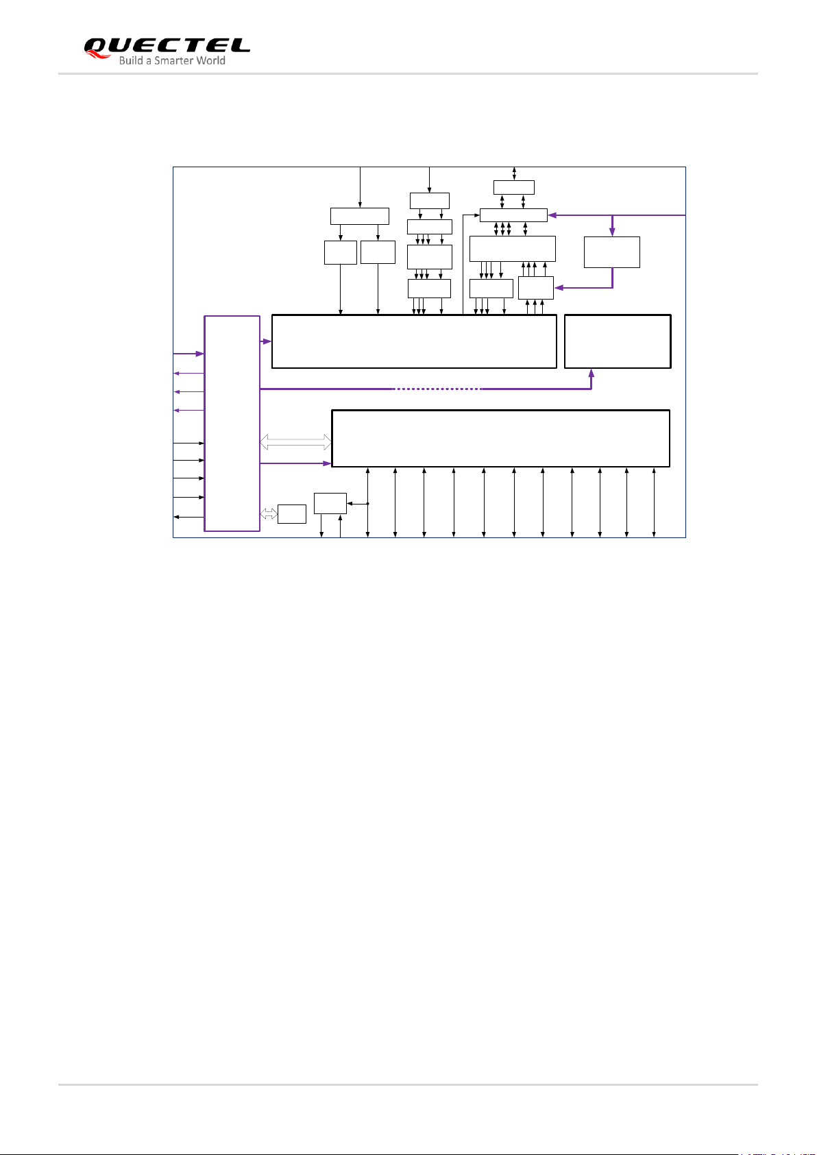
2.3. Functional Diagram
The following figure shows a block diagram of the module and illustrates the major functional parts.
⚫ Power management
⚫ Baseband
⚫ LPDDR4X + NAND flash
⚫ Radio frequency
⚫ Peripheral interfaces
NOTES
Automotive Module Series
AG521R-NA QuecOpen Hardware Design
AG521R-NA_QuecOpen_Hardware_Design 16 / 104
Baseband
PMIC
Transceiver
NAND
LPDDR4
ANT_GNSS
VBAT_BB
PWRKEY
ADCx2
VREG_UIM1
RESET_N
38.4M
XO
Control
Control
L2&L5
SAW
QLINK
Audio
SPKs MICs PCM PCIeUSB2.0&3.0 SPIx2 UARTx2 I2Cx2 SDIORGMII (U)SIMx2GPIOsI2S
VREG_UIM2
VDD_EXT
NET_STATUS
LED
DRx
SAWs
MMPA
QLNA*2
DP12T
Diplexer
Duplexers, SAWs
and Qualplexers
2G PA+DP16T
Diplexer
QLNA*2
...
...
...
...
...
...
L1
SAW
Diplexer
ANT_DIV
...
ANT_MAIN
VBAT_RF
APT or ET
Figure 1: Functional Diagram for AG521R-NA QuecOpen®
2.4. Evaluation Board
To help you develop applications conveniently with the module, Quectel supplies the evaluation board (EVB), USB
data cables, a pair of earphones, antennas and other peripherals to control or test the module. For more details, see
document [1].
Automotive Module Series
AG521R-NA QuecOpen Hardware Design
AG521R-NA_QuecOpen_Hardware_Design 17 / 104
3 Application Interfaces
3.1. General Description
The module is designed with 400 LGA pins that can be connected to cellular application platforms. Module
interfaces are described in detail in the following sub-chapters:
⚫ Power supply
⚫ (U)SIM interfaces
⚫ USB 2.0/3.0 interface
⚫ UART interfaces
⚫ I2S and I2C interfaces
⚫ SDIO interface
⚫ SPI interfaces
⚫ RGMII interface
⚫ WLAN and BT interfaces*
⚫ ADC interfaces
⚫ USB_BOOT interface
⚫ GPIO interfaces
“*” means under development.
NOTE
Automotive Module Series
AG521R-NA QuecOpen Hardware Design
AG521R-NA_QuecOpen_Hardware_Design 18 / 104
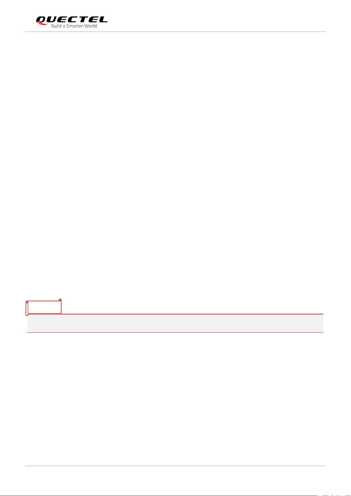
3.2. Pin Assignment
Power Pins
GND Pins RESVRVED Pins
PCIe Pins
I2S Pins
(U)SIM Pins
USB Pins
SPI Pins
SDIO Pins
RGMII Pins
306
305
304
303
302
301
300
299
298
297
296
295
294
293
292
291
290
RESERVED
RESERVED
RESERVED
RESERVED
RESERVED
RESERVED
RESERVED
RESERVED
RESERVED
RESERVED
RESERVED
RESERVED
RESERVED
RESERVED
RESERVED
RESERVED
RESERVED
196
RESERVED
RESERVED
193
190
RESERVED
184
RESERVED
187
IMU_INT2
181
IMU_PWR_EN
178
RESERVED
175
RESERVED
172
GND
169
IMU_INT1
166
RESERVED
163
RESERVED
160
GND
157
RESERVED
154
RESERVED
151
GND
148
GND
145
GND
142
RESERVED
139
RESERVED
138
GND
137
GND
141
GND
140
GND
144
GND
143
ANT_MAIN
147
GND
146
GND
150
GND
149
GND
153
GND
152
RESERVED
156
GND
155
GND
159
GND
158
GND
161
RESERVED
162
GND
164
GND
165
GND
167
GND
168
GND
171
GND
170
ANT_DIV
GND
174
173
GND
176
GND
177
GND
179
GND
RESERVED
180
GND
182
GND
182
183
GND
185
GND
186
188
RESERVED
GND
189
191
GND
192
GND
194
GND
195
GND
198
GND
197
RESERVED
199
GND
200
RESERVED
201
GND
202
GND
203
GND
204
RESERVED
205
RESERVED
206
RESERVED
GND
207
208
GND
209
GND
210
SPI1_MOSI
211
GND
212
GND
213
SPI1_CS
214
GND
GND
215
GND
216
SPI1_CLK
217
GND
218
GND
219
SPI1_MISO
220
GND
221
GND
222
WLAN_PWR_EN1
223
RESERVED
224
RESERVED
225
WLAN_PWR_EN2
226
RESERVED
227
RESERVED
228
WLEN_EN
229
RESERVED
230
GND
231
WLAN_SLP_CLK
232
GND
GND
233
234
GND
GND
235
RESERVED
236
RESERVED
237
GND
GND
238
RESERVED
239
RESERVED
240
GND
241
VBAT_BB
242
VBAT_BB
243
GPIO6
244
VBAT_BB
245
ADC1
246
GPIO7
246
247
ADC0
248
PON_1
249
GPIO8
250
USIM1_RST
251
USIM1_VDD
252
RESERVED
253
USIM1_CLK
254
USIM1_DATA
255
USIM1_DET
258
USIM2_DET
257
USIM2_DATA
256
USIM2_VDD
259
USIM2_CLK
260
USIM2_RST
261
I2S_DOUT
262
I2S_SCK
263
I2S_DIN
264
RESERVED
265
I2S_WS
266
RESERVED
267
RESERVED
268
RESERVED
269
RESERVED
270
RESERVED
271
RESERVED
272
RESERVED
1
RESERVED
2
RESERVED
3
RESERVED
4
RESERVED
RESERVED5RESERVED
6
RESERVED
9
RESERVED
8
RESET
7
PWRKEY
10
RGMII_MD_IO
11
RGMII_MD_CLK
12
GND
13
RGMII_RX_0RGMII_RX_0
14
RGMII_RX_1
15
RGMII_CTL_RX
RGMII_RX_1
16
RGMII_RX_2
17
RGMII_RX_3
18
GND
19
RGMII_CK_RX
20
RGMII_TX_0
21
RGMII_CTL_TX
22
RGMII_TX_1
23
RGMII_TX_2
24
RGMII_CK_TX
25
RGMII_TX_3
GND
26
GND
27
RGMII_PWR_EN
28
RGMII_PWR_IN
29
RGMII_INT
30
PCIE_WAKE
31
RGMII_RSTRGMII_RST
32
PCIE_RX_M
33
GND
34
PCIE_RX_P
35
RESERVED
36
PCIE_CLKREQ
37
RESERVED
38
PCIE_REFCLK_M
39
PCIE_RST
40
PCIE_REFCLK_M
41
RESERVED
42
GND
43
RESERVED
44
PCIE_TX_M
45
EMMC_PWR_EN
46
PCIE_TX_P
47
SDC1_CLK47SDC1_CLK
48
SDC1_CMD
49
SDC1_DATA_0
50
SDC1_DATA_1
51
SDC1_DATA_2
52
SDC1_DATA_3
53
SDC1_DATA_4
54
EMMC_RST
55
SDC1_DATA_558SDC1_DATA_7
56
SDC1_DATA_6
57
RESERVED
59
BT_UART_TXD
60
SDIO_VDD
61
BT_UART_RTS61BT_UART_RTS
63
BT_UART_RXD
62
BT_UART_CTS
65
RESERVED
64
RESERVED
66
BT_EN
67
COEX_UART_RXD
68
VDD_EXT
69
COEX_UART_TXD
70
UART1_TXD
71
UART1_CTS
72
UART1_RXD
73
PCM_SYNC
74
UART1_RTS
75
PCM_CLK
76
PCM_IN
78
PCM_OUT
77
CDC_RST
79
I2C1_SCL
80
I2C1_SDA
81
I2S_MCLK
82
RESERVED
83
USB_BOOT
84
USB_VBUS
85
USB_DP
86
GND
87
USB_DM
88
USB_SS_RX_M
89
RESERVED
90
USB_SS_RX_P
91
USB_SS_TX_M
92
GND
93
USB_SS_TX_P
94
RESERVED
95
DR_SYNC
96
RESERVED
97
RESERVED
98
GND
99
RESERVED
100
GPIO1
101
GPIO2
102
GPIO3
103
RESERVED
104
GPIO4
103
105
RESERVED
106
RESERVED
107
DBG_TXD
108
RESERVED
109
VBAT_RF
110
DBG_RXD
111
VBAT_RF
112
VBAT_RF
113
RESERVED
114
VBAT_RF
115
GND
115
GND
116
GPIO5
117
GND
118
GND
119
RESERVED
120
GND
121
GND
122
RESERVED
123
RESERVED
124
GND
125
GND
126
GND
127
GND
128
GND
129
GND
130
GND
131
GND
132
RESERVED
133
GND
134
GND
135
GND
136
RESERVED
273
RESERVED
275
RESERVED
274
RESERVED
276
VDD_WIFI_VM
277
VDD_WIFI_VH
278
RESERVED
279
RESERVED
280
RESERVED
281
RESERVED
282
RESERVED
283
RESERVEDRESERVED
284
RESERVEDRESERVED
285
RESERVEDRESERVED
286
RESERVED
287
RESERVEDRESERVED
288
RESERVED
289
RESERVED
398
GND
397
GND
400
GND
GND
399
GND
307
GND
308
GND
309
GND
310
GND
311
GND
312
GND
313
GND
314
GND
315
GND
GND
324
GND
323
GND
322
GND
321
GND
320
GND
319
GND
318
GND
317
GND
316
GND
326
GND
325
GND
327
GND
328
GND
329
GND
330
GND
331
GND
332
GND
333
GND
334
GND
335
GND
336
GND
337
GND
338
GND
339
GND
340
GND
341
GND
342
GND
344
GND
343
GND
345
GND
346
GND
347
GND
348
GND
349
GND
350
GND
351
GND
352
GND
353
GND
354
GND
355
GND
356
GND
357
GND
358
GND
359
GND
360
GND
361
GND
362
GND
363
GND
364
GND
365
GND
366
GND
367
GND
368
GND
369
GND
370
GND
371
GND
372
GND
373
GND
374
GND
375
GND
376
GND
377
GND
378
GND
379
GND
380
GND
381
GND
382
GND
383
GND
384
GND
385
GND
386
GND
387
GND
388
GND
389
GND
390
GND
391
GND
392
GND
393
GND
394
GND
395
GND
396
Figure 2: Pin Assignment (Top View)
Automotive Module Series
AG521R-NA QuecOpen Hardware Design
AG521R-NA_QuecOpen_Hardware_Design 19 / 104
1. Keep all RESERVED pins and unused pins unconnected.
2. GND pins should be connected to ground in the design.
3.3. Pin Description
The following tables show the pin definition of the module and the alternate functions of multiplexing pins.
Table 3: I/O Parameters Definition
Type
Description
AI
Analog input
AO
Analog output
B
Bidirectional digital with CMOS input
DI
Digital input
DO
Digital output
H
High level
IO
Bidirectional
L
Low level
OD
Open drain
PD
Pull down
PI
Power input
PO
Power output
PU
Pull up
R
Slew-rate limited
S
Schmitt trigger input
NOTES
Automotive Module Series
AG521R-NA QuecOpen Hardware Design
AG521R-NA_QuecOpen_Hardware_Design 20 / 104
Table 4: Pin Description
Power Supply
Pin Name
Pin No.
I/O
Description
DC
Characteristics
Comment
VBAT_BB
241, 242,
244
PI
Power supply for the
module’s baseband
part
Vmax = 4.3 V
Vmin = 3.3 V
Vnorm = 3.8 V
It must be provided
with sufficient current
up to 0.8 A.
VBAT_RF
109, 111,
112, 114
235, 236
238, 239
PI
Power supply for the
module’s RF part
Vmax = 4.3 V
Vmin = 3.3 V
Vnorm = 3.8 V
It must be provided
with sufficient current
up to 2 A.
VDD_EXT
68
PO
1.8 V output power
supply for external
circuits
Vnorm = 1.8 V
IOmax = 50 mA
Power supply for
external GPIO’s pull up
circuits.
LDO_2P7
57
PO
Output power supply
for SD card
Vnorm = 2.95 V
If unused, keep it open.
VDD_WIFI_V
M
276
PO
Power supply for
Wi-Fi
Vnorm = 1.35 V
If unused, keep it open.
VDD_WIFI_VH
277
PO
Power supply for
Wi-Fi
Vnorm = 1.95 V
If unused, keep it open.
GND
12, 18, 26, 33, 42, 86, 92, 98, 115, 117, 118, 120, 121, 124–131, 133–135, 137, 138, 140,
141, 144–151, 153, 155, 156, 158, 159, 160, 162, 164, 165, 167, 168, 171–174, 176, 177,
180, 182, 183, 185, 186, 189, 191, 192, 194, 195, 198, 199, 201–203, 206, 208, 209, 211,
212, 215, 217, 218, 220, 221, 230, 232, 233, 234, 237, 240, 307–400
Turn on/off
Pin Name
Pin No.
I/O
Description
DC
Characteristics
Comment
PWRKEY
7
DI
Turn on/off the
module
VIHmax = 1.89 V
VIHmin = 1.17 V
VILmax = 0.63 V
Internally pulled up to
1.8 V.
Active low.
PON_1
248
DI
Pulling it high will
turn on the module
automatically
Valid trigger range:
0.78–1.89 V.
Active high
RESET
8
DI
Reset the module
VIHmax = 1.89 V
VIHmin = 1.17 V
VILmax = 0.63 V
Internally pulled up to
1.8 V.
Active low.
(U)SIM Interfaces
Pin Name
Pin No.
I/O
Description
DC
Characteristics
Comment

Automotive Module Series
AG521R-NA QuecOpen Hardware Design
AG521R-NA_QuecOpen_Hardware_Design 21 / 104
USIM1_VDD
251
PO
(U)SIM1 card power
supply
IOmax = 50 mA For
1.8 V (U)SIM:
Vmax = 1.9 V
Vmin = 1.7 V
For 3.0 V (U)SIM:
Vmax = 3.05 V
Vmin = 2.7 V
Either 1.8 V or 3.0 V
is supported by the
module automatically.
If unused, keep it
open.
USIM1_DATA
254
IO
(U)SIM1 card data
For 1.8 V (U)SIM:
VILmax = 0.36 V
VIHmin = 1.26 V
VOLmax = 0.4 V
VOHmin = 1.44 V
For 3.0 V (U)SIM:
VILmax = 0.57 V
VIHmin = 2.0 V
VOLmax = 0.4 V
VOHmin = 2.28 V
If unused, keep it
open.
USIM1_CLK
253
DO
(U)SIM1 card clock
For 1.8 V (U)SIM:
VOLmax = 0.4 V
VOHmin = 1.44 V
For 3.0 V (U)SIM:
VOLmax = 0.4 V
VOHmin = 2.28 V
If unused, keep it
open.
USIM1_RST
250
DO
(U)SIM1 card reset
For 1.8 V (U)SIM:
VOLmax = 0.4 V
VOHmin = 1.44 V
For 3.0 V (U)SIM:
VOLmax = 0.4 V
VOHmin = 2.28 V
If unused, keep it
open.
USIM1_DET
255
DI
(U)SIM1 card
hot-plug detect
VILmin = -0.3 V
VILmax = 0.63 V
VIHmin = 1.17 V
VIHmax = 2.1 V
1.8 V power domain.
If unused, keep it
open.
USIM2_VDD
256
PO
(U)SIM2 card
power supply
For 1.8 V (U)SIM:
Vmax = 1.9 V
Vmin = 1.7 V
For 3.0 V (U)SIM:
Vmax = 3.05 V
Vmin = 2.7 V
Either 1.8 V or 3.0 V
is supported by the
module automatically.
If unused, keep it
open.

Automotive Module Series
AG521R-NA QuecOpen Hardware Design
AG521R-NA_QuecOpen_Hardware_Design 22 / 104
IOmax = 50 mA
USIM2_DATA
257
IO
(U)SIM2 card data
For 1.8 V (U)SIM:
VILmax = 0.36 V
VIHmin = 1.26 V
VOLmax = 0.4 V
VOHmin = 1.44 V
For 3.0 V (U)SIM:
VILmax = 0.57 V
VIHmin = 2.0 V
VOLmax = 0.4 V
VOHmin = 2.28 V
If unused, keep it
open.
USIM2_CLK
259
DO
(U)SIM2 card clock
For 1.8 V (U)SIM:
VOLmax = 0.4 V
VOHmin = 1.44 V
For 3.0 V (U)SIM:
VOLmax = 0.4 V
VOHmin = 2.28 V
If unused, keep it
open.
USIM2_RST
260
DO
(U)SIM2 card reset
For 1.8 V (U)SIM:
VOLmax = 0.4 V
VOHmin = 1.44 V
For 3.0 V (U)SIM:
VOLmax = 0.4 V
VOHmin = 2.28 V
If unused, keep it
open.
USIM2_DET
258
DI
(U)SIM2 card
hot-plug detect
VILmin = -0.3 V
VILmax = 0.63 V
VIHmin = 1.17 V
VIHmax = 2.1 V
1.8 V power domain.
If unused, keep it
open.
USB Interfaces
Pin Name
Pin No.
I/O
Description
DC
Characteristics
Comment
USB_VBUS
84
DI
USB connection
detect
Vmax = 5.25 V
Vmin = 3.0 V
Vnorm = 5.0 V
USB_DP
85
AI/
AO
USB differential data
bus (+)
Compliant with USB
2.0 standard
specification. Require
differential impedance
of 90 Ω.
USB_DM
87
AI/
AO
USB differential data
bus (-)
Automotive Module Series
AG521R-NA QuecOpen Hardware Design
AG521R-NA_QuecOpen_Hardware_Design 23 / 104
USB_SS_TX_P
93
AO
USB 3.0 super-speed
transmit (+)
Compliant with USB
3.0 standard
specification. Require
differential impedance
of 90 Ω.
USB_SS_TX_M
91
AO
USB 3.0 super-speed
transmit (-)
USB_SS_RX_P
90
AI
USB 3.0 super-speed
receive (+)
USB_SS_RX_M
88
AI
USB 3.0 super-speed
receive (-)
GPIO Interfaces
Pin Name
Pin No.
I/O
Description
DC
Characteristics
Comment
GPIO1
100
IO
General-purpose
input/output
VILmin = -0.3 V
VILmax = 0.63 V
VIHmin = 1.17 V
VIHmax = 2.1 V
VOLmax = 0.45 V
VOHmin = 1.35 V
1.8 V power domain.
If unused, keep them
open.
GPIO2
101
IO
General-purpose
input/output
GPIO3
102
IO
General-purpose
input/output
GPIO4
104
IO
General-purpose
input/output
GPIO5
116
IO
General-purpose
input/output
GPIO6
243
IO
General-purpose
input/output
GPIO7
246
IO
General-purpose
input/output
GPIO8
249
DO
General-purpose
output
VILmin = TBD
VILmax = 0.63 V
VIHmin = 0.9 V
VIHmax = TBD
VOLmax = 0.36 V
VOHmin = 1.44 V
UART1 Interface
Pin Name
Pin No.
I/O
Description
DC
Characteristics
Comment
UART1_CTS
71
DO
UART1 clear to send
VOLmax = 0.45 V
VOHmin = 1.35 V
1.8 V power domain.
Can be configured to
GPIOs.
If unused, keep them
open.
UART1_RTS
74
DI
UART1 request to
send
VILmin = -0.3 V
VILmax = 0.63 V
VIHmin = 1.17 V
VIHmax = 2.1 V

Automotive Module Series
AG521R-NA QuecOpen Hardware Design
AG521R-NA_QuecOpen_Hardware_Design 24 / 104
UART1_TXD
70
DO
UART1 transmit
VOLmax = 0.45 V
VOHmin = 1.35 V
UART1_RXD
72
DI
UART1 receive
VILmin = -0.3 V
VILmax = 0.63 V
VIHmin = 1.17 V
VIHmax = 2.1 V
BT UART Interface
Pin Name
Pin No.
I/O
Description
DC
Characteristics
Comment
BT_UART_TXD
59
DO
BT UART transmit
VOLmax = 0.45 V
VOHmin = 1.35 V
1.8 V power domain.
Can be configured to
GPIO.
If unused, keep them
open.
BT_UART_RXD
63
DI
BT UART receive
VILmin = -0.3 V
VILmax = 0.63 V
VIHmin = 1.17 V
VIHmax = 2.1 V
BT_UART_RTS
61
DI
BT UART request to
send
VILmin = -0.3 V
VILmax = 0.63 V
VIHmin = 1.17 V
VIHmax = 2.1 V
BT_UART_CTS
62
DO
BT UART clear to
send
VOLmax = 0.45 V
VOHmin = 1.35 V
Debug UART Interface
Pin Name
Pin No.
I/O
Description
DC
Characteristics
Comment
DBG_RXD
110
DI
Debug UART receive
VILmin = -0.3 V
VILmax = 0.63 V
VIHmin = 1.17 V
VIHmax = 2.1 V
1.8 V power domain.
DBG_TXD
107
DO
Debug UART
transmit
VOLmax = 0.45 V
VOHmin = 1.35 V
I2C1 Interface (for Codec Configuration by Default)
Pin Name
Pin No.
I/O
Description
DC
Characteristics
Comment
I2C1_SCL
79
OD
I2C1 serial clock
External pull-up
resistor is required.
1.8 V only.
Can be configured to
GPIO.
If unused, keep them
open.
I2C1_SDA
80
OD
I2C1 serial data
Automotive Module Series
AG521R-NA QuecOpen Hardware Design
AG521R-NA_QuecOpen_Hardware_Design 25 / 104
I2S Interface (for Codec Configuration by Default)
Pin Name
Pin No.
I/O
Description
DC
Characteristics
Comment
CDC_RST
77
DO
Codec reset
VOLmax = 0.45 V
VOHmin = 1.35 V
1.8 V power domain.
Can be configured to
GPIO.
If unused, keep them
open.
I2S_MCLK
81
DO
Clock output for
codec
VOLmax = 0.45 V
VOHmin = 1.35 V
I2S_WS
265
IO
I2S word select
VOLmax = 0.45 V
VOHmin = 1.35 V
VILmin = -0.3 V
VILmax = 0.63 V
VIHmin = 1.17 V
VIHmax = 2.1 V
I2S_SCK
262
DO
I2S clock
VOLmax = 0.45 V
VOHmin = 1.35 V
I2S_DIN
263
DI
I2S data in
VILmin = -0.3 V
VILmax = 0.63 V
VIHmin = 1.17 V
VIHmax = 2.1 V
I2S_DOUT
261
DO
I2S data out
VOLmax = 0.45 V
VOHmin = 1.35 V
PCM Interface
Pin Name
Pin No.
I/O
Description
DC
Characteristics
Comment
PCM_SYNC
73
IO
PCM data frame sync
VOLmax = 0.45 V
VOHmin = 1.35 V
VILmin = -0.3 V
VILmax = 0.63 V
VIHmin = 1.17 V
VIHmax = 2.1 V
1.8 V power domain.
Can be configured to
GPIO.
If unused, keep them
open.
PCM_CLK
75
IO
PCM clock
VOLmax = 0.45 V
VOHmin = 1.35 V
VILmin = -0.3 V
VILmax = 0.63 V
VIHmin = 1.17 V
VIHmax = 2.1 V
PCM_IN
76
DI
PCM data input
VILmin = -0.3 V
VILmax = 0.63 V
VIHmin = 1.17 V
VIHmax = 2.1 V
PCM_OUT
78
DO
PCM data output
VOLmax = 0.45 V
VOHmin = 1.35 V
Automotive Module Series
AG521R-NA QuecOpen Hardware Design
AG521R-NA_QuecOpen_Hardware_Design 26 / 104
PCIe Interface
Pin Name
Pin No.
I/O
Description
DC
Characteristics
Comment
PCIE_REFCLK_
P
40
AO
PCIe reference clock
(+)
Require differential
impedance of 95 Ω.
If unused, keep them
open.
PCIE_REFCLK_
M
38
AO
PCIe reference clock
(-)
PCIE_TX_M
44
AO
PCIe transmit (-)
PCIE_TX_P
46
AO
PCIe transmit (+)
PCIE_RX_M
32
AI
PCIe receive (-)
PCIE_RX_P
34
AI
PCIe receive (+)
PCIE_CLKREQ
36
IO
PCIe clock request
VOLmax = 0.45 V
VOHmin = 1.35 V
VILmin = -0.3 V
VILmax = 0.63 V
VIHmin = 1.17 V
VIHmax = 2.1 V
1.8 V power domain
If unused, keep them
open.
PCIE_RST
39
DO
PCIe reset
VOLmax = 0.45 V
VOHmin = 1.35 V
PCIE_WAKE
30
DI
PCIe wakeup
VILmin = -0.3 V
VILmax = 0.63 V
VIHmin = 1.17 V
VIHmax = 2.1 V
RGMII Interface
Pin Name
Pin No.
I/O
Description
DC
Characteristics
Comment
RGMII_MD_IO
10
IO
RGMII MDIO
management data
Power domain
determined by
RGMII_PWR_IN
If unused, keep them
open.
RGMII_MD_
CLK
11
DO
RGMII MDC
management clock
RGMII_RX_0
13
DI
RGMII receive data
bit 0
RGMII_RX_1
14
DI
RGMII receive data
bit 1
RGMII_CTL_RX
15
DI
RGMII receive
control
RGMII_RX_2
16
DI
RGMII receive data
bit 2

Automotive Module Series
AG521R-NA QuecOpen Hardware Design
AG521R-NA_QuecOpen_Hardware_Design 27 / 104
RGMII_RX_3
17
DI
RGMII receive data
bit 3
RGMII_CK_RX
19
DI
RGMII receive clock
RGMII_TX_0
20
DO
RGMII transmit data
bit 0
RGMII_CTL_TX
21
DO
RGMII transmit
control
RGMII_TX_1
22
DO
RGMII transmit data
bit 1
RGMII_TX_2
23
DO
RGMII transmit data
bit 2
RGMII_CK_TX
24
DO
RGMII transmit clock
RGMII_TX_3
25
DO
RGMII transmit data
bit 3
RGMII_PWR_
EN
27
DO
Enable external LDO
to supply power to
RGMII_PWR_IN
VOLmax = 0.45 V
VOHmin = 1.35 V
1.8 V power domain.
If unused, keep it
open.
RGMII_PWR_IN
28
PI
Power input for
internal RGMII
circuit
1.8/2.5 V power
supply input.
If RGMII is not be
used, connect it to
VDD_EXT.
RGMII_INT
29
DI
RGMII PHY interrupt
output
VILmin = -0.3 V
VILmax = 0.63 V
VIHmin = 1.17 V
VIHmax = 2.1 V
1.8 V power domain.
If unused, keep them
open.
RGMII_RST
31
DO
Reset output for
RGMII PHY
VOLmax = 0.45 V
VOHmin = 1.35 V
SDIO Interface (for eMMC by default)
Pin Name
Pin No.
I/O
Description
DC
Characteristics
Comment
SDIO_VDD
60
PI
SDIO power supply
connect it to
VDD_EXT.
SDC1_DATA_0
49
IO
SDIO data bit 0
VOLmax = 0.45 V
VOHmin = 1.4 V
VILmin = -0.3 V
VILmax = 0.58 V
VIHmin = 1.27 V
VIHmax = 2.0 V
1.8 V power domain
for eMMC
applications.
If unused, keep it
open.
SDC1_DATA_1
50
IO
SDIO data bit 1
SDC1_DATA_2
51
IO
SDIO data bit 2
SDC1_DATA_3
52
IO
SDIO data bit 3

Automotive Module Series
AG521R-NA QuecOpen Hardware Design
AG521R-NA_QuecOpen_Hardware_Design 28 / 104
SDC1_CMD
48
IO
SDIO command
SDC1_DATA_4
53
IO
SDIO data bit 4
VOLmax = 0.45 V
VOHmin = 1.35 V
VILmin = -0.3 V
VILmax = 0.63 V
VIHmin = 1.17 V
VIHmax = 2.1 V
1.8 V power domain
Can be configured to
GPIOs.
If unused, keep them
open.
SDC1_DATA_5
55
IO
SDIO data bit 5
SDC1_DATA_6
56
IO
SDIO data bit 6
SDC1_DATA_7
58
IO
SDIO data bit 7
SDC1_CLK
47
DO
SDIO clock
VOLmax = 0.45 V
VOHmin = 1.4 V
1.8 V power domain
for eMMC
applications.
If unused, keep it
open.
EMMC_RST
54
DO
eMMC reset
VOLmax = 0.45 V
VOHmin = 1.35 V
1.8 V power domain.
If unused, keep it
open.
EMMC_PWR_E
N
45
DO
eMMC power supply
enable control
VOLmax = 0.45 V
VOHmin = 1.35 V
1.8 V power domain.
If unused, keep it
open.
SPI Interfaces
Pin Name
Pin No.
I/O
Description
DC
Characteristics
Comment
SPI1_CLK
216
DO
SPI1 clock
VOLmax = 0.45 V
VOHmin = 1.35 V
1.8 V power domain.
If unused, keep them
open.
Can be configured
into GPIOs.
SPI1_CS
213
DO
SPI1 chip select
VOLmax = 0.45 V
VOHmin = 1.35 V
SPI1_MISO
219
DI
SPI1 master-in
salve-out
VILmin = -0.3 V
VILmax = 0.63 V
VIHmin = 1.17 V
VIHmax = 2.1 V
SPI1_MOSI
210
DO
SPI1 master-out
slave-in
VOLmax = 0.45 V
VOHmin = 1.35 V
ADC Interfaces
Pin Name
Pin No.
I/O
Description
DC
Characteristics
Comment
ADC0
247
AI
General-purpose ADC
interface
Voltage Range:
0–1.875 V
If unused, keep it
open.
ADC1
245
AI
General-purpose ADC
interface
Voltage Range:
0–1.875 V
If unused, keep it
open.
Other Interface Pins

Automotive Module Series
AG521R-NA QuecOpen Hardware Design
AG521R-NA_QuecOpen_Hardware_Design 29 / 104
Pin Name
Pin No.
I/O
Description
DC
Characteristics
Comment
USB_BOOT
83
DI
Force the module into
emergency download
mode
1.8 V power domain.
If unused, keep it
open.
BT_EN
66
DO
BT function enable
control
VOLmax = 0.45 V
VOHmin = 1.35 V
DR_SYNC
95
DO
Navigation 1PPS time
sync output
VOLmax = 0.45 V
VOHmin = 1.35 V
IMU_INT1
169
DI
IMU interrupt 1
VILmin = -0.3 V
VILmax = 0.63 V
VIHmin = 1.17 V
VIHmax = 2.1 V
1.8 V power domain.
Can be configured to
GPIOs.
If unused, keep them
open.
IMU_INT2
187
DI
IMU interrupt 2
VILmin = -0.3 V
VILmax = 0.63 V
VIHmin = 1.17 V
VIHmax = 2.1 V
IMU_PWR_EN
181
DO
IMU power enable
control
VOLmax = 0.45 V
VOHmin = 1.35 V
WLAN Interface
Pin Name
Pin No.
I/O
Description
DC
Characteristics
Comment
WLAN_PWR_
EN2
225
DO
WLAN power supply
enable control 2
VOLmax = 0.45 V
VOHmin = 1.35 V
1.8 V power domain.
If unused, keep them
open.
1.8 V power domain.
If unused, keep them
open.
WLAN_PWR_
EN1
222
DO
WLAN power supply
enable control 1
VOLmax = 0.45 V
VOHmin = 1.35 V
WLAN_EN
228
DO
WLAN enable
VOLmax = 0.45 V
VOHmin = 1.35 V
COEX_UART_
RXD
67
DI
LTE&WLAN/BT
coexistence receive
VILmin = -0.3 V
VILmax = 0.63 V
VIHmin = 1.17 V
VIHmax = 2.1 V
COEX_UART_
TXD
69
DO
LTE&WLAN/BT
coexistence transmit
VOLmax = 0.45 V
VOHmin = 1.35 V
WLAN_SLP_
CLK
231
DO
WLAN sleep clock
VOLmax = 0.45 V
VOHmin = 1.35 V
RF Antenna Interfaces

Automotive Module Series
AG521R-NA QuecOpen Hardware Design
AG521R-NA_QuecOpen_Hardware_Design 30 / 104
1. Keep all RESERVED pins and unused pins unconnected.
2. GND pins should be connected to ground in the design.
Pin Name
Pin No.
I/O
Description
DC
Characteristics
Comment
ANT_MAIN
143
AI/
AO
Main antenna
interface
50 Ω impedance.
ANT_DIV
170
AI
Diversity antenna
interface
RESERVED Pins
Pin Name
Pin No.
Comment
RESERVED
1-6, 9, 35, 37, 41, 43, 64, 65, 82, 89, 94, 96, 97, 99, 103, 105, 106,
108, 113, 119, 122, 123, 132, 136, 139, 142, 152, 154, 157, 161,
163, 166, 175, 178, 179, 184, 188, 190, 193, 196, 197, 200, 204,
205, 207, 214, 223, 224, 226, 227, 229, 252, 264, 266–275,
278–306
Keep these pins open.
NOTES

Automotive Module Series
AG521R-NA QuecOpen Hardware Design
AG521R-NA_QuecOpen_Hardware_Design 31 / 104
Table 5: Alternate Functions of Multiplexing Pins
Pin
No.
Pin Name
Default
Function
Alternate Function 1
Alternate Function 2
Reset
1)
Wake up
Interrupt 2)
Power Domain
Remark
27
RGMII_PWR_EN
RGMII
BS-PD, L
Y
1.8 V
29
RGMII_INT
BS-PD, L
Y
1.8 V
31
RGMII_RST
BS-PD, L
Y
1.8 V
30
PCIE_WAKE
PCIe
BS-PD, L
Y
1.8 V
36
PCIE_CLKREQ
BS-PD, L
Y
1.8 V
39
PCIE_RST
BS-PD, L
Y
1.8 V
45
EMMC_PWR_EN
SDIO
BS-PD, L
Y
1.8 V
53
SDC1_DATA_4
GPIO_92
BSH-PD, L
N
1.8 V
54
EMMC_RST
BS-PD, L
Y
1.8 V
55
SDC1_DATA_5
GPIO_93
BSH-PD, L
Y
1.8 V
56
SDC1_DATA_6
GPIO_94
BSH-PD, L
Y
1.8 V
58
SDC1_DATA_7
GPIO_95
BSH-PD, L
Y
1.8 V
59
BT_UART_TXD
UART
GPIO_63
BS-PD, L
N
1.8 V
61
BT_UART_RTS
GPIO_65
BS-PD, L
Y
1.8 V
62
BT_UART_CTS
GPIO_66
BS-PD, L
N
1.8 V
63
BT_UART_RXD
GPIO_64
BS-PD, L
Y
1.8 V
67
COEX_UART_RXD
BS-PD, L
Y
1.8 V
69
COEX_UART_TXD
BS-PD, L
N
1.8 V
BOOT_CONFIG_0
70
UART1_TXD
GPIO_20
BS-PD, L
N
1.8 V

Automotive Module Series
AG521R-NA QuecOpen Hardware Design
AG521R-NA_QuecOpen_Hardware_Design 32 / 104
71
UART1_CTS
GPIO_23
BS-PD, L
N
1.8 V
72
UART1_RXD
GPIO_21
BS-PU, L
Y
1.8 V
74
UART1_RTS
GPIO_22
BS-PD, L
Y
1.8 V
107
DBG_TXD
BS-PD, L
N
1.8 V
110
DBG_RXD
BS-PD, L
Y
1.8 V
73
PCM_SYNC
PCM
I2S_WS
GPIO_12
BS-PD, L
Y
1.8 V
75
PCM_CLK
I2S_SCK
GPIO_15
BS-PD, L
Y
1.8 V
76
PCM_IN
I2S_DIN
GPIO_13
BS-PD, L
Y
1.8 V
78
PCM_OUT
I2S_DOUT
GPIO_14
BS-PD, L
Y
1.8 V
77
CDC_RST
I2S
GPIO_86
BS-PD, L
Y
1.8 V
81
I2S_MCLK
GPIO_62
BS-PD, L
N
1.8 V
261
I2S_DOUT
PCM_OUT
GPIO_18
BS-PD, L
Y
1.8 V
262
I2S_SCK
PCM_CLK
GPIO_19
BS-PD, L
Y
1.8 V
263
I2S_DIN
PCM_IN
GPIO_17
BS-PD, L
Y
1.8 V
265
I2S_WS
PCM_SYNC
GPIO_16
BS-PD, L
Y
1.8 V
79
I2C1_SCL
I2C
BSR-PD, L
Y
1.8 V
80
I2C1_SDA
BSR-PD, L
Y
1.8 V
250
USIM1_RST
(U)SIM
BSH-PD, L
N
1.8/2.85 V
253
USIM1_CLK
BSH-PD, L
N
1.8/2.85 V
254
USIM1_DATA
BSH-PD, L
N
1.8/2.85 V
255
USIM1_DET
BS-PD, L
Y
1.8 V
260
USIM2_RST
BSH-PD, L
Y
1.8/2.85 V

Automotive Module Series
AG521R-NA QuecOpen Hardware Design
AG521R-NA_QuecOpen_Hardware_Design 33 / 104
259
USIM2_CLK
BSH-PD, L
N
1.8/2.85 V
257
USIM2_DATA
BSH-PD, L
N
1.8/2.85 V
258
USIM2_DET
BS-PD, L
Y
1.8 V
210
SPI1_MOSI
SPI
GPIO_72
BS-PD, L
N
1.8 V
213
SPI1_CS
GPIO_74
BS-PD, L
N
1.8 V
216
SPI1_CLK
GPIO_75
BS-PD, L
Y
1.8 V
219
SPI1_MISO
GPIO_73
BS-PD, L
N
1.8 V
66
BT_EN
Others
BS-PD, L
Y
1.8 V
83
USB_BOOT
BS-PD, L
N
1.8 V
95
DR_SYNC
BS-PD, L
Y
1.8 V
169
IMU_INT1
GPIO_88
BS-PD, L
Y
1.8 V
181
IMU_PWR_EN
GPIO_91
BS-PD, L
N
1.8 V
187
IMU_INT2
GPIO_82
BS-PD, L
Y
1.8 V
222
WLAN_PWR_EN1
BS-PD, L
Y
1.8 V
225
WLAN_PWR_EN2
BS-PD, L
Y
1.8 V
228
WLAN_EN
BS-PD, L
Y
1.8 V
100
GPIO1
GPIO
BS-PD, L
Y
1.8 V
101
GPIO2
BS-PD, L
Y
1.8 V
102
GPIO3
BS-PD, L
N
1.8 V
104
GPIO4
BS-PD, L
N
1.8 V
116
GPIO5
BS-PD, L
N
1.8 V
243
GPIO6
BS-PD, L
N
1.8 V

Automotive Module Series
AG521R-NA QuecOpen Hardware Design
AG521R-NA_QuecOpen_Hardware_Design 34 / 104
1. “Alternate Function 1/2” takes effect only after software configuration.
2. 1) See Table 4 for more details about the symbol description.
3. 2) If the GPIOs without interrupt function are configured as interrupt GPIOs, power consumption of the module will be increased. (“Y” means “interrupt function supported”. “N” means “interrupt function not
supported”.)
4. Pins 69 and 83 cannot be pulled up before power-up.
246
GPIO7
BS-PD, L
Y
1.8 V
249
GPIO8
L
N
1.8 V
NOTES

Automotive Module Series
AG521R-NA QuecOpen Hardware Design
AG521R-NA_QuecOpen_Hardware_Design 35 / 104
3.4. Operating Modes
The table below briefly summarizes the various operating modes referred in the following chapters.
Table 6: Overview of Operating Modes
Mode
Details
Normal Operation
Idle
Software is active. The module has registered on the network, and it is
ready to send and receive data.
Talk/Data
Network connection is ongoing. In this mode, the power consumption is
decided by network setting and data transfer rate.
Minimum
Functionality Mode
AT+CFUN=0 can set the module into a minimum functionality mode without removing
the power supply. In this case, both RF function and (U)SIM card will be invalid.
Airplane Mode
AT+CFUN=4 can set the module into airplane mode. In this case, RF function will be
invalid.
Sleep Mode
In this mode, the current consumption of the module will be reduced to the minimal level.
During this mode, the module can still receive paging message, SMS, voice call and
TCP/UDP data from the network normally.
Power Down Mode
In this mode, the power management unit shuts down the power supply. Software is not
active. The serial interfaces are not accessible. Operating voltage (connected to
VBAT_RF and VBAT_BB) remains applied.
3.5. Power Saving
3.5.1. Sleep Mode
The module is able to reduce its current consumption to a minimum value during the sleep mode. This chapter
mainly introduces some ways to enter or exit from sleep mode. The diagram below illustrates the current
consumption of the module during sleep mode.
Current
Run Time
DRX OFF ON OFF
ON ON OFF OFF
ON
OFF

Automotive Module Series
AG521R-NA QuecOpen Hardware Design
AG521R-NA_QuecOpen_Hardware_Design 36 / 104
Figure 3: Sleep Mode Current Consumption Diagram
DRX cycle index values are broadcasted by the base station through the wireless network.
3.5.1.1. USB Application with USB Remote Wakeup Function
If the host supports USB suspend/resume and remote wakeup function, the following three preconditions must be
met to let the module enter sleep mode.
⚫ Use sleep API to enable the sleep mode.
⚫ Ensure the level of pins that configured as wake-up interrupt in Table 5 are under non-wakeup status.
⚫ The host’s USB bus, which is connected with the module’s USB interface, enters suspended state.
The following figure shows the connection between the module and the host.
USB Interface
VDD
USB Interface
Module
Host
GND
GND
USB_VBUS
Figure 4: Sleep Mode Application with USB Remote Wakeup
⚫ Sending data to the module through USB will wake up the module.
⚫ When the module has URC to report, it will send remote wake-up signals via USB bus so as to wake up the
host.
3.5.1.2. USB Application without USB Remote Wakeup Function
If the host supports USB suspend/resume, but does not support remote wake-up function, it needs to be woken up
via the module’s GPIO.
There are three preconditions to let the module enter sleep mode.
NOTE

Automotive Module Series
AG521R-NA QuecOpen Hardware Design
AG521R-NA_QuecOpen_Hardware_Design 37 / 104
⚫ Use sleep & wakeup API to enable the sleep mode.
⚫ Ensure the level of pins that configured as wake-up interrupt in Table 5 are under non-wakeup status.
⚫ The host’s USB bus, which is connected with the module’s USB interface, enters suspended state.
The following figure shows the connection between the module and the host.
USB Interface
VDD
USB Interface
Module
Host
GND
GND
USB_VBUS
GPIO
EINT
Figure 5: Sleep Mode Application without USB Remote Wakeup
⚫ Sending data to the module through USB will wake up the module.
⚫ When the module has URC to report, the module’s GPIO signal can be used to wake up the host.
3.5.1.3. USB Application without USB Suspend Function
If the host does not support USB suspend function, USB_VBUS should be connected with an external control
circuit to set the module to sleep mode.
⚫ Use sleep API to enable the sleep mode.
⚫ Ensure the level of pins that configured as wake-up interrupt in Table 5 are under non-wakeup status.
⚫ Disconnect USB_VBUS.
The following figure shows the connection between the module and the host.
USB Interface
VDD
USB Interface
Module
Host
GND
GND
USB_VBUS
GPIO
EINT
Power
Switch
GPIO

Automotive Module Series
AG521R-NA QuecOpen Hardware Design
AG521R-NA_QuecOpen_Hardware_Design 38 / 104
Figure 6: Sleep Mode Application without Suspend Function
Switching on the power switch to supply power to USB_VBUS will wake up the module.
Please pay attention to the level match shown in dotted line between the module and the host.
3.5.2. Airplane Mode
When the module enters airplane mode, the RF function does not work, and all AT commands correlative with RF
function will be inaccessible. The mode can be set via AT+CFUN=<fun> command. The parameter <fun>
indicates the module’s functionality levels, as shown below.
⚫ AT+CFUN=0: Minimum functionality mode. Both (U)SIM and RF functions are disabled.
⚫ AT+CFUN=1: Full functionality mode (by default).
⚫ AT+CFUN=4: Airplane mode. RF function is disabled.
3.6. Power Supply
3.6.1. Power Supply Pins
The module provides seven VBAT pins for connection with an external power supply.
⚫ Three VBAT_BB pins for module’s baseband part.
⚫ Four VBAT_RF pins for module’s RF part.
Table 7: VBAT and GND Pins
Pin Name
Pin No.
Description
Min.
Typ.
Max.
Unit
VBAT_BB
241, 242, 244
Power supply for the
module’s baseband part
3.3
3.8
4.3 V VBAT_RF
109, 111, 112, 114
235, 236, 238, 239
Power supply for the
module’s RF part
3.3
3.8
4.3
V
GND
12, 18, 26, 33, 42, 86, 92, 98, 115, 117, 118, 120, 121, 124–131,133–135, 137, 138, 140, 141,
144–151,153, 155, 156, 158, 159, 160, 162, 164, 165, 167, 168, 171–174,176, 177, 180, 182,
183, 185, 186, 189, 191, 192, 194, 195, 198, 199, 201–203, 206, 208, 209, 211, 212, 215, 217,
218, 220, 221, 230, 232, 233, 234, 237, 240, 307–400
NOTE

Automotive Module Series
AG521R-NA QuecOpen Hardware Design
AG521R-NA_QuecOpen_Hardware_Design 39 / 104
3.6.2. Decrease Voltage Drop
The power supply range of the module is from 3.3 to 4.3 V. Please make sure that the input voltage will never drop
below 3.3 V. The following figure shows the voltage drop during burst transmission in 2G network. The voltage
drop will be less in 3G and 4G networks.
VBAT
Burst
Transmission
Min.3.3V
Ripple
Drop
Burst
Transmission
Figure 7: Power Supply Limits during Burst Transmission
To decrease voltage drop, a bypass capacitor of about 100 µF with low ESR should be used, and a multi-layer
ceramic chip capacitor (MLCC) array should also be reserved due to its low ESR. It is recommended to use three
ceramic capacitors (100 nF, 33 pF, 10 pF) for composing the MLCC array, and place these capacitors close to
VBAT pins. DC_3V8 from an external application has to be a single voltage source and can be expanded to two sub
paths with star structure. The width of VBAT_BB trace should be no less than 1 mm. The width of VBAT_RF trace
should be no less than 2 mm. In principle, the longer the VBAT trace is, the wider it will be.
In addition, in order to get a stable power source, it is suggested to use high power TVS diode to prevent static
electricity, and place them as close to the VBAT pins as possible. The following figure shows a reference design of
VBAT power supply pins.
DC_3V8
C1
100 µF
+
3
D1
C
33 pF
C
100 nF
2
C
10 pF
4
VBAT_BB
Module
VBAT_RF
C6
100 nF
C7
33 pF
C8
10 pF
+
C
5
100 µF
Figure 8: VBAT Reference Design

Automotive Module Series
AG521R-NA QuecOpen Hardware Design
AG521R-NA_QuecOpen_Hardware_Design 40 / 104
3.6.3. Reference Design for Power Supply
Power design for the module is very important, as the performance of the module largely depends on the power
source. If the voltage drop between the input and output is not too high, it is recommended to use an LDO to supply
power for the module. If there is a big voltage difference between the input source and the desired output (VBAT),
a buck converter is preferred to be used as the power supply.
The following figure shows a reference design for 12/24 V input power source. The designed output for the power
supply is about 3.8 V and the maximum rated current is 5 A.
2
4
1
3
6
7
8
182K
NM
100K
10 pF
100 pF
100 nF
10 µF
470 µF
100 nF
100 nF
DC_IN
100 µH
5V_EN
100 nF
BOOT
VIN
EN
RT/CLK
SW
GND
COMP
FB
GND
TPS54560-Q1
7.2 µH
9
5
220 µF
1 µF
10 nF
4.3K
4.7 nF
4.7 pF
75k
20k
DC_3V8
Figure 9: 12/24 V Power Supply System Reference Design
To avoid damaging internal flash, do not switch off the power supply when the module works normally. Only after
the module is turned off by PWRKEY, the power supply can be cut off.
3.6.4. Monitor the Power Supply
API can be used to monitor the VBAT_BB voltage value. For more details, see document [2].
3.7. Power on and off Scenarios
3.7.1. Turn on Module with PWRKEY
Table 8: PWRKEY Pin Description
Pin Name
Pin No.
Description
DC Characteristics
Comment
NOTE

Automotive Module Series
AG521R-NA QuecOpen Hardware Design
AG521R-NA_QuecOpen_Hardware_Design 41 / 104
PWRKEY
7
Turn on/off the module
VIHmax = 1.89 V
VIHmin = 1.17 V
VILmax = 0.63 V
1.8 V power domain.
Pulled-up internally.
Active low.
When the module is in power-off mode, it can be turned on by driving PWRKEY low for at least 500 ms. It is
recommended to use an open drain/collector driver to control the PWRKEY. A simple reference circuit is illustrated
in the following figure.
Turn on pulse
PWRKEY
4.7K
47K
500 ms
Figure 10: Turn on the Module Using Driving Circuit
Another way to control the PWRKEY is using a button directly. When pressing the key, electrostatic strike may
generate from the finger. Therefore, a TVS component is indispensable to be placed nearby the button for ESD
protection. A reference circuit is shown in the following figure.
PWRKEY
S1
Close to S1
TVS
Figure 11: Turn on the Module Using Keystroke
The power on scenario is illustrated in the following figure.

Automotive Module Series
AG521R-NA QuecOpen Hardware Design
AG521R-NA_QuecOpen_Hardware_Design 42 / 104
V
IL
≤
0.63 V
V
IH
≥
1.17 V
VBAT
PWRKEY
RESET
Inactive
ActiveUART
Note 1
Inactive
Active
USB
TBD
TBD
VDD_EXT
TBD
≥ 500 ms
Figure 12: Power-on Timing
1. Please make sure that VBAT is stable for at least 30 ms before pulling down PWRKEY pin.
2. It is recommended to use an external OD/OC circuit to control the PWRKEY pin.
3.7.2. Turn on Module with PON_1
Table 9: PON_1 Pin Description
Pin Name
Pin No.
Description
Comment
PON_1
248
Driving it high will turn on the module
automatically
Valid trigger range:
0.78 V~1.89 V.
When the module is powered off, drive PON_1 high for at least 500 ms will turn on the module automatically. A
simple reference circuit is illustrated in the following figure.
NOTES

Automotive Module Series
AG521R-NA QuecOpen Hardware Design
AG521R-NA_QuecOpen_Hardware_Design 43 / 104
PVIN
SS/TR
Module
PON_1
10K
0.78–1.89 V
Figure 13: Turn on the Module using PON_1
If PON_1 is not used, it is recommended to connect it to the ground.
3.7.3. Turn off Module
Either of the following methods can be used to turn off the module:
⚫ Normal power down procedure: Turn off the module using the PWRKEY pin.
⚫ Normal power down procedure: Turn off the module using API interface.
3.7.3.1. Turn off Module Using PWRKEY
Driving PWRKEY low for at least 2 s, the module will execute power-down procedure after PWRKEY is released.
The power-off scenario is illustrated in the following figure.
VBAT
PWRKEY
TBD
2 s
RUNNING
Power
-
down procedure
OFF
Module
Status
VDD_EXT
Figure 14: Power-off Timing
NOTE

Automotive Module Series
AG521R-NA QuecOpen Hardware Design
AG521R-NA_QuecOpen_Hardware_Design 44 / 104
3.7.3.2. Turn off Module Using API Interface
It is also a safe way to use API interface to turn off the module, which is similar to turning off the module via
PWRKEY Pin.
See document [2] for details about API function.
1. To avoid damaging the internal flash, please do not switch off the power supply when the module works
normally. Only after the module is shut down by PWRKEY or API interface, the power supply can be cut off.
2. When turn off module with API, please keep PWRKEY at high level after the execution of power off
command. Otherwise the module will be turned on again after successfully turn-off.
3.8. Reset the Module
RESET can be used to reset the module. The module can be reset by driving RESET low for at least 370 ms. As
the RESET pin is sensitive to interference, the routing trace is recommended to be as short as possible and totally
ground shielded.
Table 10: RESET Pin Description
Pin Name
Pin No.
Description
DC Characteristics
Comment
RESET
8
Reset the module
VIHmax = 1.89 V
VIHmin = 1.17 V
VILmax = 0.63 V
The recommended circuit is similar to the PWRKEY control circuit. An open drain/collector driver or button can be
used to control the RESET.
NOTES

Automotive Module Series
AG521R-NA QuecOpen Hardware Design
AG521R-NA_QuecOpen_Hardware_Design 45 / 104
Reset pulse
RESET
4.7K
47K
370–620 ms
Figure 15: Reference Circuit of RESET by Using Driving Circuit
RESET
S2
Close to S2
TVS
Figure 16: Reference Circuit of RESET by Using Button
The reset scenario is illustrated in the following figure.
VIL≤ 0.63 V
VIH≥ 1.17 V
VBAT
≥ 370 ms
Resetting
Module
Status
Running
RESET
Restart
620 ms
Figure 17: Timing of Resetting Module
NOTE

Automotive Module Series
AG521R-NA QuecOpen Hardware Design
AG521R-NA_QuecOpen_Hardware_Design 46 / 104
Please assure that there is no large capacitance on PWRKEY and RESET pins.
3.9. (U)SIM Interfaces
The (U)SIM interface circuitry meets ETSI and IMT-2000 requirements. Both 1.8 V and 3.0 V (U)SIM cards are
supported.
Table 11: Pin Definition of (U)SIM Interface
The module supports (U)SIM card hot-plug via the USIM_DET pin and either low level or high level detection is
supported. The function is disabled by default and can be enabled by AT+QSIMDET. See document [3] for more
details of the command.
The following figure shows a reference design for (U)SIM interface with an 8-pin (U)SIM card connector.
Pin Name
Pin No.
I/O
Description
Comment
USIM1_VDD
251
PO
(U)SIM1 card power supply
Either 1.8 V or 3.0 V is supported
by the module automatically.
USIM1_DATA
254
IO
(U)SIM1 card data
USIM1_CLK
253
DO
(U)SIM1 card clock
USIM1_RST
250
DO
(U)SIM1 card reset
USIM1_DET
255
DI
(U)SIM1 card hot-plug detect
USIM2_VDD
256
PO
(U)SIM2 card power supply
USIM2_DATA
257
IO
(U)SIM2 card data
USIM2_CLK
259
DO
(U)SIM2 card clock
USIM2_RST
260
DO
(U)SIM2 card reset
USIM2_DET
258
DI
(U)SIM2 card hot-plug detect

Automotive Module Series
AG521R-NA QuecOpen Hardware Design
AG521R-NA_QuecOpen_Hardware_Design 47 / 104
Module
USIM_VDD
USIM_RST
USIM_CLK
USIM_DATA
USIM_DET
22R
22R
22R
VDD_EXT
470K
100 nF (U)SIM Card Connector
GND
GND
VCC
RST
CLK
IO
VPP
GND
USIM_VDD
10K
33 pF 33 pF33 pF
CD1 CD2
Figure 18: Reference Circuit of (U)SIM Interface with an 8-Pin (U)SIM Card Connector
If (U)SIM card detection function is not needed, keep USIM_DET disconnected.
A reference circuit for (U)SIM interface with a 6-pin (U)SIM card connector is illustrated in the following figure.
Module
USIM_VDD
USIM_RST
USIM_CLK
USIM_DATA
22R
22R
22R
100 nF
(U)SIM Card Connector
GND
VCC
RST
CLK IO
VPP
GND
10K
USIM_VDD
33 pF 33 pF33 pF
Figure 19: Reference Circuit of (U)SIM Interface with a 6-Pin (U)SIM Card Connector
To enhance the reliability and availability of the (U)SIM card, follow the criteria below in the (U)SIM circuit
design:
⚫ Keep the placement of (U)SIM card connector as close to the module as possible. Keep the trace length as less
than 200 mm as possible.
⚫ Keep (U)SIM card signals away from RF and VBAT traces.
⚫ Assure the trace between the ground of the module and that of the (U)SIM card connector short and wide.
Keep the trace width of ground and USIM_VDD no less than 0.5 mm to maintain the same electric potential.
⚫ To avoid cross-talk between USIM_DATA and USIM_CLK, keep them away from each other and shield them

Automotive Module Series
AG521R-NA QuecOpen Hardware Design
AG521R-NA_QuecOpen_Hardware_Design 48 / 104
with surrounded ground.
⚫ In order to offer good ESD protection, it is recommended to add a TVS diode array with parasitic capacitance
not exceeding 10 pF. The 22 Ω resistors should be added in series between the module and the (U)SIM card
connector so as to suppress EMI spurious transmission and enhance ESD protection. The 33 pF capacitors are
used for filtering interference of EGSM900. Please note that the (U)SIM peripheral circuit should be close to
the (U)SIM card connector.
⚫ The pull-up resistor on USIM_DATA line can improve anti-jamming capability when long layout trace and
sensitive occasions are applied, and should be placed close to the (U)SIM card connector.
⚫
The load capacitance of (U)SIM interface will affect rise and fall time of the data exchange.
3.10. USB Interfaces
The module provides one USB 3.0 interface and one USB 2.0 interface which support SuperSpeed (5 Gbps on
USB 3.0) and High-Speed (480 Mbps on USB 2.0) modes.
The USB 3.0 interface is used for data communication with AP by default. The USB 2.0 interface supports AT
command communication, data transmission, software debugging, firmware upgrade and voice over USB*.
Table 12: Pin Description of USB Interface
Pin Name
Pin No.
I/O
Description
Comment
USB_VBUS
84
DI
USB connection detect
USB_DP
85
AI/AO
USB differential data bus (+)
Compliant with USB 2.0
standard specification.
Require differential
impedance of 90 Ω.
USB_DM
87
AI/AO
USB differential data bus (-)
USB_SS_TX_P
93
AO
USB 3.0 super-speed transmit (+)
Compliant with USB 3.0
standard specification.
Require differential
impedance of 90 Ω.
USB_SS_TX_M
91
AO
USB 3.0 super-speed transmit (-)
USB_SS_RX_P
90
AI
USB 3.0 super-speed receive (+)
USB_SS_RX_M
88
AI
USB 3.0 super-speed receive (-)
It is recommended to reserve USB 2.0 for firmware upgrade in application design, and reserve test points for
debugging purpose. The following are the reference circuits of USB 3.0 and 2.0 interfaces.
NOTE

Automotive Module Series
AG521R-NA QuecOpen Hardware Design
AG521R-NA_QuecOpen_Hardware_Design 49 / 104
USB_DP
USB_DM
GND
USB_DP
USB_DM
GND
L1
Close to Module
R1
R2
Test Points
NM_0R
NM_0R
Minimize these stubs
Module
Connector
ESD Array
USB_VBUS
USB_VBUS
Figure 20: Reference Circuit of USB 2.0 Application
C1
100 nF
C2
100 nF
C3
100 nF
C4
100 nF
USB_VBUS
Module
USB_SS_TX_P
USB_VBUS
USB_SS_TX_M
USB_SS_RX_P
USB_SS_RX_M
USB_SS_RX_P
USB_SS_RX_M
USB_SS_TX_P
USB_SS_TX_M
AP
Figure 21: Reference Circuit of USB 3.0 Application
To ensure signal integrity of USB data lines, components R1, R2 and L1 must be placed close to the module, and
also these resistors should be placed close to each other. The capacitors C1 and C2 should be placed near the
module. The capacitors C3 and C4 should be placed near the AP. The extra stubs of trace must be as short as
possible.
The following principles of USB interface should be complied with, so as to meet USB 2.0 and USB 3.0
specifications.
⚫ It is important to route the USB 2.0 and 3.0 signal traces as differential pairs with ground surrounded.
The impedance of USB differential trace is 90 Ω.
⚫ For USB 2.0 signal traces, the trace length should be less than 120 mm, and the differential data pair matching
should be less than 0.7 mm (5 ps).
⚫ For USB 3.0 signal traces, the maximum length of each differential data pair (Tx/Rx) is recommended to be
less than 100 mm, and each differential data pair matching should be less than 0.7 mm (5 ps).

Automotive Module Series
AG521R-NA QuecOpen Hardware Design
AG521R-NA_QuecOpen_Hardware_Design 50 / 104
⚫ Do not route signal traces under crystals, oscillators, magnetic devices, PCIe and RF signal traces. It
is important to route the USB differential traces in inner-layer with ground shielding on not only upper
and lower layers but also right and left sides.
⚫ If a USB connector is used, please keep the ESD protection components as close to the USB connector as
possible. Pay attention to the influence of junction capacitance of ESD protection components on USB data
lines. Typically, the capacitance value should be less than 2.0 pF for USB 2.0, and less than 0.4 pF for USB
3.0.
1. USB 2.0 and USB 3.0 share the same controller, therefore they cannot be used simultaneously.
2. “*” means under development.
3.11. UART Interfaces
The module provides three UART interfaces: UART1, BT UART and debug UART.
⚫ UART1 and BT UART support RTS and CTS hardware flow control, and are used for data transmission with
peripherals.
⚫ UART1 and BT UART support 4800, 9600, 19200, 38400, 57600, 115200, 230400, 460800 and 921600 bps
baud rates, and the default is 115200 bps.
⚫ The debug UART interface supports 115200 bps baud rate, and is used for Linux console and log output.
Table 13: Pin Definition of UART1 Interface
Pin Name
Pin No.
I/O
Description
Comment
UART1_CTS
71
DO
UART1 clear to send
1.8 V power domain.
Can be configured to GPIOs.
UART1_RTS
74
DI
UART1 request to send
UART1_TXD
70
DO
UART1 transmit
UART1_RXD
72
DI
UART1 receive
Table 14: Pin Definition of BT UART Interface
Pin Name
Pin No.
I/O
Description
Comment
BT_UART_TXD
59
DO
BT UART transmit
1.8 V power domain.
NOTES

Automotive Module Series
AG521R-NA QuecOpen Hardware Design
AG521R-NA_QuecOpen_Hardware_Design 51 / 104
Table 15: Pin Definition of Debug UART Interface
Pin Name
Pin No.
I/O
Description
Comment
DBG_TXD
107
DO
Debug UART transmit
1.8 V power domain.
DBG_RXD
110
DI
Debug UART receive
1.8 V power domain.
Table 16: Logic Levels of Digital I/O
Parameter
Min.
Max.
Unit
VIL
-0.3
0.63
V
VIH
1.17
2.1
V
VOL 0 0.45
V
VOH
1.35
1.8
V
The module provides 1.8 V UART interfaces. A level translator should be used if customers’ application is
equipped with a 3.3 V UART interface. A level translator TXS0104E-Q1 provided by Texas Instruments (visit
http://www.ti.com for more information) is recommended. The following figure shows a reference design.
VCCA VCCB
OE
A1
A2
A3
A4
NC
GND
B1
B2
B3
B4
NC
VDD_1V8
CTS
RTS
RXD
TXD
0.1 μF
0.1 μF
CTS_MCU
RTS_MCU
RXD_MCU
TXD_MCU
VDD_MCU
Translator
Figure 22: Reference Circuit with Translator Chip
Another example with transistor translation circuit is shown as below. The circuit design of dotted line section can
refer to the design of solid line section, in terms of both module input and output circuit designs, but please pay
BT_UART_RXD
63
DI
BT UART receive
Can be configured to GPIOs
BT_UART_RTS
61
DI
BT UART request to send
BT_UART_CTS
62
DO
BT UART clear to send

Automotive Module Series
AG521R-NA QuecOpen Hardware Design
AG521R-NA_QuecOpen_Hardware_Design 52 / 104
attention to the direction of connection.
MCU/ARM
TXD
RXD
VDD_1V8
10K
VCC_MCU
4.7K
10K
VDD_1V8
TXD
RXD
RTS
CTS
RTS
CTS
GND
Module
VDD_1V8
4.7K
GND
1 nF
1 nF
Figure 23: Reference Circuit with Transistor Circuit
1. Transistor circuit solution is not suitable for applications with high baud rates exceeding 460 kbps.
2. For the purpose of reducing power consumption, it is recommended to switch off the power supply for
VDD_1V8 in sleep mode.
3. Please note that the module CTS is connected to the host CTS, and the module RTS is connected to the host
RTS.
3.12. I2S and I2C Interfaces
The module provides I2S and I2C interfaces for audio function design.
Table 17: Pin Definition of I2S Interface
Pin Name
Pin No.
I/O
Description
Comment
CDC_RST
77
DO
Codec reset
1.8 V power domain.
Can be configured to GPIOs.
I2S_MCLK
81
DO
Clock output for codec
I2S_WS
265
IO
I2S word select
I2S_SCK
262
DO
I2S clock
I2S_DIN
263
DI
I2S data in
NOTES

Automotive Module Series
AG521R-NA QuecOpen Hardware Design
AG521R-NA_QuecOpen_Hardware_Design 53 / 104
Table 18: Pin Definition of I2C Interface
Pin Name
Pin No.
I/O
Description
Comment
I2C1_SCL
79
OD
I2C serial clock
Require external pull-up to 1.8 V.
I2C1_SDA
80
OD
I2C serial data
The following figure shows a reference design of I2S and I2C interfaces with an external codec IC.
CDC_RST
I2S_MCLK
I2S_CLK
I2S_WS
I2S_DIN
I2S_DOUT
I2C1_SCL
I2C1_SDA
Module
BIAS
INP
INN
LOUTP
LOUTN
Codec
RESET
MCLK
BCLK
WCLK
DOUT
DIN
SCL
SDA
1.8V
2.2K
2.2K
Figure 24: Reference Circuit of I2S and I2C Application with Audio Codec
The module works as a master device pertaining to I2C interface.
3.13. SDIO Interface
The module provides an SDIO interface. It is recommended to use the interface for eMMC application.
Table 19: Pin Definition of SDIO Interface
I2S_DOUT
261
DO
I2S data out
Pin Name
Pin No.
I/O
Description
Comment
NOTE

Automotive Module Series
AG521R-NA QuecOpen Hardware Design
AG521R-NA_QuecOpen_Hardware_Design 54 / 104
The following is a reference design of SDIO interface for eMMC application.
SDIO_VDD
60
PI
SDIO power supply
Connect it to VDD_EXT.
SDC1_DATA_0
49
IO
SDIO data bit 0
1.8 V power domain for eMMC.
SDC1_DATA_1
50
IO
SDIO data bit 1
SDC1_DATA_2
51
IO
SDIO data bit 2
SDC1_DATA_3
52
IO
SDIO data bit 3
SDC1_CMD
48
IO
SDIO command
SDC1_DATA_4
53
IO
SDIO data bit 4
1.8 V power domain.
For eMMC configuration by default.
Can be configured to GPIO.
SDC1_DATA_5
55
IO
SDIO data bit 5
SDC1_DATA_6
56
IO
SDIO data bit 6
SDC1_DATA_7
58
IO
SDIO data bit 7
SDC1_CLK
47
DO
SDIO clock
1.8 V power domain for eMMC.
EMMC_RST
54
DO
eMMC reset
1.8 V power domain.
EMMC_PWR_EN
45
DO
eMMC power supply
enable control

Automotive Module Series
AG521R-NA QuecOpen Hardware Design
AG521R-NA_QuecOpen_Hardware_Design 55 / 104
R12
NM
R13
NM
R14
NM
R15
NM
R16
NM
R17
NM
R18
NM
R19
NM
R20
10K
R21
47K
VDD_1V8
C1
NM
C2
NM
C3
NM
C4
NM
C5
NM
C6
NM
C7
NM
C8
NM
C9
NM
C10
NM
C11
NM
VDD_3V
C14
100 nF
C15
2.2 µF
VDD_1.8V
C12
100 nF
C13
1 µF
DAT0
DAT1
DAT2
DAT3
DAT4
DAT5
DAT6
DAT7
CMD
CLK
RSTN
VCCQ
VCC
VSS
eMMC
EMMC_PWR_EN
SDC1_DATA_0
SDC1_DATA_1
SDC1_DATA_2
SDC1_DATA_3
SDC1_DATA_4
SDC1_DATA_5
SDC1_DATA_6
SDC1_DATA_7
SDC1_CMD
SDC1_CLK
EMMC_RST
EMMC_PWR_EN
SDIO_VDD
Module
R1 0R
R2 0R
R3 0R
R4 0R
R5 0R
R6 0R
R7 0R
R8 0R
R9 0R
R10 30-35R
R11 0R
VDD_EXT
Figure 25: Reference Design of SDIO Interface for eMMC Application
Please follow the principles below in eMMC circuit design:
⚫ To avoid jitter of bus, it is recommended to reserve resistors R12–R21 for pulling up SDIOs to
VDD_1.8 V. Resistors R12–R19 are not mounted by default, and the recommended resistor value is
10–100 kΩ.
⚫ In order to improve signal quality, it is recommended to add 0 Ω resistors R1–R9 and R11 in series
between the module and eMMC. Resistor R10 should be 30-35 Ω. The bypass capacitors C1–C11
are reserved and not mounted by default. All resistors and bypass capacitors should be placed close
to the module.
⚫ It is important to route the SDIO signal traces with total grounding. The impedance of SDIO data
trace is 50 Ω (±10%).
⚫ Keep SDIO signals far away from other sensitive circuits/signals such as RF circuits and analog
signals as well as noisy signals such as clock signals and DC-DC signals.
⚫ Spacing DATA to DATA/CLK bus is larger than two times of line width.
⚫ Spacing DATA/CLK/CMD to other signals is larger than two times of line width.
⚫ It is recommended to keep the trace length difference between CLK and DATA/CMD less than 1 mm
and the total routing length less than 50 mm. The total trace length inside the module is 17 mm, so
the exterior total trace length should be less than 33 mm.
⚫ Make sure the adjacent trace spacing is two times of the trace width and the load capacitance of
SDIO bus should be less than 40 pF.

Automotive Module Series
AG521R-NA QuecOpen Hardware Design
AG521R-NA_QuecOpen_Hardware_Design 56 / 104
3.14. SPI Interfaces
The module provides two SPI interfaces supporting only master mode. The maximum clock frequency of SPI is up
to 50 MHz.
Table 20: Pin Definition of SPI Interfaces
The following figure shows the timing relationship of SPI interfaces. The related parameters of SPI timing are
shown in the table below.
SPI_CS
SPI_CLK
SPI_MOSI
SPI_MISO
MSB
1 2 3
T
t(mov)
4
t(mis)
t(mih)
t(ch)
t(cl)
Figure 26: SPI Timing
Table 21: Parameters of SPI Interface Timing
Pin Name
Pin No.
I/O
Description
Comment
SPI1_CLK
216
DO
SPI1 clock
1.8 V power domain.
Can be configured to GPIO.
If unused, keep them open.
SPI1_CS
213
DO
SPI1 chip select
SPI1_MISO
219
DI
SPI1 master-in salve-out
SPI1_MOSI
210
DO
SPI1 master-out slave-in
Parameter
Description
Min.
Typ.
Max.
Unit
T
SPI clock period
20.0
- - ns
t(ch)
SPI clock high-level time
9.0 - -
ns

Automotive Module Series
AG521R-NA QuecOpen Hardware Design
AG521R-NA_QuecOpen_Hardware_Design 57 / 104
The module provides a 1.8 V SPI interface. A level translator should be used between the module and the host if
customers’ application is equipped with a 3.3 V processor or device interface.
3.15. RGMII Interface
The module includes an integrated Ethernet MAC with an RGMII interface. Key features of the RGMII interface
are shown below:
⚫ Support IEEE 1588-2008, IEEE 802.1AS-2011 and 802.1-Qav-2009
⚫ Half/full duplex for 10/100/1000 Mbps
⚫ Support VLAN tagging
⚫ Can be used to connect to external Ethernet PHY like 88EA1512, or an external switch
Table 22: Pin Definition of RGMII Interface
t(cl)
SPI clock low-level time
9.0 - -
ns
t(mov)
SPI master data output valid time
-5.0 - 5.0
ns
t(mis)
SPI master data input setup time
5.0 - -
ns
t(mih)
SPI master data input hold time
1.0 - -
ns
Pin Name
Pin No.
I/O
Description
Comment
RGMII_MD_IO
10
IO
RGMII MDIO management data
Power domain determined by
RGMII_PWR_IN
RGMII_MD_CLK
11
DO
RGMII MDC management clock
RGMII_RX_0
13
DI
RGMII receive data bit 0
RGMII_RX_1
14
DI
RGMII receive data bit 1
RGMII_CTL_RX
15
DI
RGMII receive control
RGMII_RX_2
16
DI
RGMII receive data bit 2
RGMII_RX_3
17
DI
RGMII receive data bit 3
RGMII_CK_RX
19
DI
RGMII receive clock
NOTE

Automotive Module Series
AG521R-NA QuecOpen Hardware Design
AG521R-NA_QuecOpen_Hardware_Design 58 / 104
The following figure shows the simplified block diagram for Ethernet application.
Module
Ethernet
PHY
CMC
RGMII
MDIO
RXD
TXD
MDIO
MDIP/N
Figure 27: Simplified Block Diagram for Ethernet Application
The following figure shows a reference design of RGMII interface with PHY application.
RGMII_TX_0
20
DO
RGMII transmit data bit 0
RGMII_CTL_TX
21
DO
RGMII transmit control
RGMII_TX_1
22
DO
RGMII transmit data bit 1
RGMII_TX_2
23
DO
RGMII transmit data bit 2
RGMII_CK_TX
24
DO
RGMII transmit clock
RGMII_TX_3
25
DO
RGMII transmit data bit 3
RGMII_PWR_EN
27
DO
Enable external LDO to supply
power to RGMII_PWR_IN
1.8 V power domain
RGMII_PWR_IN
28
PI
Power input for internal RGMII
circuit
1.8/2.5 V
power supply input.
If RGMII interface is not
used, please connect it to
VDD_EXT.
RGMII_INT
29
DI
RGMII PHY interrupt output
1.8 V power domain
RGMII_RST
31
DO
Reset output for RGMII PHY

Automotive Module Series
AG521R-NA QuecOpen Hardware Design
AG521R-NA_QuecOpen_Hardware_Design 59 / 104
R13 R14 R15 R16
RGMII_VDDO
R1 0R
R2 0R
R3 0R
R4 0R
R5 0R
R6 0R
R7 0R
R8 0R
R9 0R
R10 0R
R11 0R
R12 0R
RGMII_PWR_EN
RGMII_PWR_IN
RGMII_VDDO
RGMII_RX_0
RGMII_RX_1
RGMII_RX_2
RGMII_RX_3
RGMII_CTL_RX
RGMII_CK_RX
RGMII_TX_0
RGMII_TX_1
RGMII_TX_2
RGMII_TX_3
RGMII_CTL_TX
RGMII_CK_TX
RGMII_PWR_EN
Module
RGMII_RST
RGMII_INT
RGMII_MD_CLK
RGMII_MD_IO
RGMII_PWR_IN
MDIO
INTN
RESETN
Ethernet PHY
MDC
RXD0
RXD1
RXD2
RXD3
RXC
RCLK
TXD0
TXD1
TXD2
TXD3
RCLK
RXC
VDDO
Figure 28: Reference Circuit of RGMII Interface with PHY Application
In order to enhance the reliability and availability of customers’ application, please follow the criteria below in the
Ethernet PHY circuit design:
⚫ The I/O voltage of RGMII matches with that of PHY.
⚫ The voltage of RGMII_INT and RGMII_RST matches with the I/O voltage of PHY.
⚫ The typical power consumption of RGMII_PER_IN is 300 mA @ 1.8 V.
⚫ Keep RGMII data and control signals away from RF and VBAT traces.
⚫ Assure impedance of RGMII signals trace is 50 Ω ±20%.
⚫ The length difference among CK_TX, CTL_TX and TX_[0-3] is less than 2 mm.
⚫ The length difference among CK_RX, CTL_RX and RX_[0-3] is less than 2 mm.
⚫ TX bus (CK_TX to CTL_TX/TX_[0-3]) spacing or RX bus (CK_RX to CTL_RX/RX_[0-3]) spacing is larger
than two times of the line width.
⚫ Spacing between TX bus and RX bus is larger than 2.5 times of line width.
⚫ Spacing to all other signals is larger than three times of line width.
⚫ Resistors R7–R12 should be placed near the module. Resistor R1–R6 should be placed near the Ethernet PHY.

Automotive Module Series
AG521R-NA QuecOpen Hardware Design
AG521R-NA_QuecOpen_Hardware_Design 60 / 104
The value of R1–R16 varies with the selection of PHY.
3.16. WLAN and BT Interfaces*
The module provides a PCIe interface for WLAN function and UART & PCM interfaces for BT function.
Table 23: Pin Definition of WLAN and BT Interfaces
Pin Name Pin No. I/O Description Comment
PCIe Interface
PCIE_REFCLK_P
40
AO
PCIe reference clock (+)
Require differential
impedance of 95 Ω.
PCIE_REFCLK_M
38
AO
PCIe reference clock (-)
PCIE_TX_M
44
AO
PCIe transmit (-)
PCIE_TX_P
46
AO
PCIe transmit (+)
PCIE_RX_M
32
AI
PCIe receive (-)
PCIE_RX_P
34
AI
PCIe receive (+)
PCIE_CLKREQ
36
DI
O
PCIe clock request
1.8 V power domain.
PCIE_RST
39
DO
PCIe reset
PCIE_WAKE
30
DI
PCIe wakeup
Coexistence Interface
COEX_UART_
RXD
67
DI
LTE&WLAN/BT
coexistence receive
1.8 V power domain.
COEX_UART_
TXD
69
DO
LTE&WLAN/BT
coexistence transmit
BT Interface
BT_UART_TXD
59
DO
BT UART transmit
1.8 V power domain.
Can be configured to
BT_UART_RXD
63
DI
BT UART receive
BT_UART_RTS
61
DI
BT UART request to send

Automotive Module Series
AG521R-NA QuecOpen Hardware Design
AG521R-NA_QuecOpen_Hardware_Design 61 / 104
1. When WLAN or BT function is used, the coexistence interface must be used simultaneously.
2. When BT function is enabled on the module, PCM_SYNC and PCM_CLK pins will only be used to output
signals.
3. It is recommended that the networks of PCIE_CLKREQ and PCIE_WAKE are pulled up to VDD_EXT.
4. “*” means under development.
The following figure shows a reference design for WLAN and BT interfaces application.
BT_UART_CTS
62
DO
BT UART clear to send
GPIOs.
PCM_SYNC
73
IO
PCM data frame sync
PCM_CLK
75
IO
PCM data bit clock
PCM_IN
76
DI
PCM data input
PCM_OUT
78
DO
PCM data output
Others interfaces
WLAN_PWR_EN2
225
DO
WLAN power supply enable control
2
1.8 V power domain.
WLAN_PWR_EN1
222
DO
WLAN power supply enable control
1
WLAN_EN
228
DO
WLAN enable
BT_EN
66
DO
BT function enable
WLAN_SLP_CLK
231
DO
WLAN sleep clock
VDD_WIFI_VM
276
PO
Power supply for Wi-Fi
Vnorm = 1.35 V
VDD_WIFI_VH
277
PO
Power supply for Wi-FI
Vnorm = 1.95 V
NOTES

Automotive Module Series
AG521R-NA QuecOpen Hardware Design
AG521R-NA_QuecOpen_Hardware_Design 62 / 104
PCIE_TX_M
PCIE_TX_P
PCIE_RST
PCIE_RX_P
COEX_UART_ RXD
BT_UART_TXD
BT_UART_CTS
PCM_SYNC
Module
PCIE_REFCLK_M
PCIE_REFCLK_P
PCIE_WAKE
PCIE_CLKREQ
PCM_CLK
PCIE_RX_M
COEX_UART_ TXD
BT_UART_RXD
BT_UART_RTS
PCM_IN
PCM_OUT
WLAN_EN
BT_EN
WLAN_SLP_CLK
WLAN_PWR_EN1
WLAN_PWR_EN2
PCIE_CLKREQ_N
WLAN&BT PHY
PCIE_WAKE
PCIE_RST
PCIE_REFCLKP
PCIE_REFCLKM
PCIE_RXM
PCIE_RXP
PCIE_TXP
PCIE_TXM
COEX_UART_ RXD
COEX_UART_ TXD
BT_UART_TXD
BT_UART_RXD
BT_UART_CTS
BT_UART_RTS
PCM_CLK
PCM_SYNC
PCM_IN
PCM_OUT
WLAN_EN
BT_EN
SLEEP_CLK
R1
100KR2100K
VDD_EXT
WLAN_PWR_EN1
WLAN_PWR_EN2
VDD_WIFI_VM
VDD_WIFI_VH
VDD_WIFI_VM
VDD_WIFI_VH
C1
100 nF
C2
100 nF
C3
100 nF
C4
100 nF
Figure 29: Reference Circuit for Connection with WLAN&BT PHY
To ensure the signal integrity of PCIe interface, C1 and C2 should be placed close to the module. C3 and C4 should
be placed close to the PHY. The extra stubs of trace must be as short as possible.

Automotive Module Series
AG521R-NA QuecOpen Hardware Design
AG521R-NA_QuecOpen_Hardware_Design 63 / 104
The following principles of PCIe interface design should be complied with, so as to meet PCIe Gen2 specifications.
⚫ It is important to route the PCIe signal traces as differential pairs with ground surrounded. And the differential
impedance is 95 Ω ±10%.
⚫ For PCIe signal traces, the maximum length of each differential data pair (TX/RX/REFCLK) is recommended
to be less than 270 mm, and each differential data pair matching should be less than 0.7 mm (5 ps).
⚫ Spacing data lane-to-lane (intra-interface) is three times of line width.
⚫ Spacing to all other signals (inter-interface) is four times of line width.
⚫ Do not route signal traces under crystals, oscillators, magnetic devices or RF signal traces. It is
important to route the PCIe differential traces in inner-layer with ground shielding on not only upper
and lower layers but also right and left sides.
3.17. ADC Interfaces
The module provides three analog-to-digital converter (ADC) interfaces. The voltage value on ADC pins can be
read via AT+QADC=<port> command, through specifying <port> as 0, 1 or 2. For more details about the AT
command, see document [3].
⚫ AT+QADC=0: read the voltage value on ADC0
⚫ AT+QADC=1: read the voltage value on ADC1
In order to improve the accuracy of ADC, the traces of ADC interfaces should be surrounded by ground.
Table 24: Pin Definition of ADC Interfaces
Pin Name
Pin No.
Description
ADC1
245
General purpose ADC interface
ADC0
247
General purpose ADC interface
Table 25: Characteristic of ADC Interface
Parameter
Min.
Typ.
Max.
Unit
ADC0 Voltage Range
0 1.875
V
ADC1 Voltage Range
0 1.875
V
ADC Resolution
14 bits

Automotive Module Series
AG521R-NA QuecOpen Hardware Design
AG521R-NA_QuecOpen_Hardware_Design 64 / 104
1. The input voltage for each ADC interface must not exceed its corresponding voltage range.
2. It is prohibited to supply any voltage to ADC pins when VBAT is removed.
3. It is recommended to use resistor divider circuit for ADC application.
3.18. USB_BOOT Interface
The module provides a USB_BOOT pin. Pulling up the USB_BOOT to VDD_EXT before powering on the module
will force the module into emergency download mode when powered on. In emergency download mode, the
module supports firmware upgrade over USB 2.0 interface.
Table 26: Pin Definition of USB_BOOT Interface
Pin Name
Pin No.
I/O
Description
Comment
USB_BOOT
83
DI
Force the module into emergency
download mode
1.8 V power domain.
Active high.
If unused, keep it open.
The following figure shows a reference circuit of USB_BOOT interface.
Module
USB_BOOT
VDD_EXT
10K
Test point
TVS
Close to module
Figure 30: Reference Circuit of USB_BOOT Interface
3.19. GPIO Interfaces
The module provides 8 GPIOs.
ADC Sample Rate
4.8 MHz
NOTES

Automotive Module Series
AG521R-NA QuecOpen Hardware Design
AG521R-NA_QuecOpen_Hardware_Design 65 / 104
Table 27: Pin Definition of GPIOs
Pin Name
Pin No.
I/O
Description
Comment
GPIO1
100
IO
General-purpose input/output
1.8 V power domain. If
unused, keep them open.
GPIO2
101
IO
GPIO3
102
IO
GPIO4
104
IO
GPIO5
116
IO
GPIO6
243
IO
GPIO7
246
IO
GPIO8
249
DO

Automotive Module Series
AG521R-NA QuecOpen Hardware Design
AG521R-NA_QuecOpen_Hardware_Design 66 / 104
4 Antenna Interfaces
The module includes one main antenna interface (ANT_MAIN) and one Rx-diversity antenna interface (ANT_DIV)
which is used to resist the fall of signals caused by high speed movement and multipath effect. The antenna ports
have an impedance of 50 Ω.
4.1. Main/Rx-diversity Antenna Interface
4.1.1. Pin Definition
The pin definition of Main/Rx-diversity antenna interfaces are shown below.
Table 28: Pin Definition of Main/Rx-diversity Antenna Interfaces
Pin Name
Pin No.
I/O
Description
Comment
ANT_MAIN
143
AI/AO
Main antenna interface
50 Ω impedance
ANT_DIV
170
AI
Receive diversity antenna interface
50 Ω impedance
4.1.2. Operating Frequency
Table 29: Module Operating Frequencies
3GPP Band
Transmit
Receive
Unit
WCDMA B2
1850-1910
1930-1990
MHz
WCDMA B4
1710-1755
2110-2155
MHz
WCDMA B5
824~849
869~894
MHz
LTE-FDD B2
1850-1910
1930-1990
MHz
LTE-FDD B4
1710-1755
2110-2155
MHz
LTE-FDD B25
1850-1915
1930-1995
MHz

Automotive Module Series
AG521R-NA QuecOpen Hardware Design
AG521R-NA_QuecOpen_Hardware_Design 67 / 104
LTE-FDD B66
1710-1780
2110-2200
MHz
LTE-FDD B12
699-716
729-746
MHz
LTE-FDD B13
777-787
746-756
MHz
LTE-FDD B14
788-798
758-768
MHz
LTE-FDD B17
704-716
734-746
MHz
LTE-FDD B26
814-849
859~894
MHz
LTE-FDD B5
824~849
869~894
MHz
LTE-FDD B30
/
2350-2360
MHz
LTE-FDD B7
2500~2570
2620~2690
MHz
LTE-FDD B71
663-698
617-652
MHz
LTE-FDD B29
2 )
/
717-728
MHz
1.
1)
LTE-FDD B29, B30 and B32 support Rx only.
4.1.3. Reference Design of RF Antenna Interfaces
A reference design of main and Rx-diversity antenna interfaces is shown as below. It is recommended to reserve a
π-type matching circuit for better RF performance, and the π-type matching components (R1/C1/C2 and R2/C3/C4)
should be placed as close to the antennas as possible. The capacitors are not mounted by default.
NOTE

Automotive Module Series
AG521R-NA QuecOpen Hardware Design
AG521R-NA_QuecOpen_Hardware_Design 68 / 104
ANT_MAIN
R1 0R
C1
Module
Main
Antenna
NM
C2
NM
R2 0R
C3
Diversity
Antenna
NM
C4
NM
ANT_DIV
Figure 31: Reference Circuit of RF Antenna Interfaces
ANT_DIV function is enabled by default. AT+QCFG="diversity",0 command can be used to disable receive
diversity. See document [3] for details of the command.
4.1.4. Reference Design of RF Layout
For user’s PCB, the characteristic impedance of all RF traces should be controlled to 50 Ω. The impedance of the
RF traces is usually determined by the trace width (W), the materials’ dielectric constant, the height from the
reference ground to the signal layer (H), and the spacing between RF traces and grounds (S). Microstrip or coplanar
waveguide is typically used in RF layout to control characteristic impedance. The following are reference designs
of microstrip or coplanar waveguide with different PCB structures.
Figure 32: Microstrip Design on a 2-layer PCB
NOTES

Automotive Module Series
AG521R-NA QuecOpen Hardware Design
AG521R-NA_QuecOpen_Hardware_Design 69 / 104
Figure 33: Coplanar Waveguide Design on a 2-layer PCB
Figure 34: Coplanar Waveguide Design on a 4-layer PCB (Layer 3 as Reference Ground)
Figure 35: Coplanar Waveguide Design on a 4-layer PCB (Layer 4 as Reference Ground)
To ensure RF performance and reliability, the following principles should be complied with in RF layout design:
⚫ Use an impedance simulation tool to accurately control the characteristic impedance of RF traces to 50 Ω.
⚫ The GND pins adjacent to RF pins should not be designed as thermal relief pads, and should be fully
connected to ground.

Automotive Module Series
AG521R-NA QuecOpen Hardware Design
AG521R-NA_QuecOpen_Hardware_Design 70 / 104
⚫ The distance between the RF pins and the RF connector should be as short as possible, and all the right-angle
traces should be changed to curved ones. The recommended trace angle is 135°.
⚫ There should be clearance under the signal pin of the antenna connector or solder joint.
⚫ The reference ground of RF traces should be complete. Meanwhile, adding some ground vias around RF traces
and the reference ground could help to improve RF performance. The distance between the ground vias and
RF traces should be no less than two times the width of RF signal traces (2 × W).
⚫ Keep RF traces away from interference sources, and avoid intersection and paralleling between traces on
adjacent layers.
For more details about RF layout, see document [4].
4.2. Antenna Installation
4.2.1. Antenna Requirements
The following table shows the requirements on the main antenna and the Rx-diversity antenna.
Table 30: Antenna Requirements
Type
Requirements
UMTS/LTE
VSWR: ≤ 2
Efficiency: > 30%
Max input power: 50 W
Input impedance: 50 Ω
Cable insertion loss: < 1 dB
(WCDMA B5/B8/B19, LTE-FDD
B5/B8/B9/B12/B13/B17/B18/B19/B20/B26/B28/B29/B71)
Cable insertion loss: < 1.5 dB
(WCDMA B1/B2/B3/B4B9, LTE-FDD
B1/B2/B3/B4/B9/B11/B21/B25/B32/B66, LTE-TDD B34/B39)
Cable insertion loss: < 2 dB
(LTE-FDD B7/B30, LTE-TDD B38/B40/B41)

Automotive Module Series
AG521R-NA QuecOpen Hardware Design
AG521R-NA_QuecOpen_Hardware_Design 71 / 104
4.2.2. Recommended RF Connector for Antenna Installation
If RF connector is used for antenna connection, it is recommended to use the HFM connector provided by
Rosenberger.
Figure 36: Description of the HFM Connector
For more details, visit https://www.rosenbergerap.com.

Automotive Module Series
AG521R-NA QuecOpen Hardware Design
AG521R-NA_QuecOpen_Hardware_Design 72 / 104
5 Reliability, Radio and Electrical
Characteristics
5.1. Absolute Maximum Ratings
Absolute maximum ratings for power supply and voltage on digital and analog pins of the module are listed in the
following table.
Table 31: Absolute Maximum Ratings
Parameter
Min.
Max.
Unit
VBAT_RF/VBAT_BB
-0.3
6.0 V USB_VBUS
-0.3
5.5 V Peak Current of VBAT_BB
0
0.8 A Peak Current of VBAT_RF
0
2.0 A Voltage at Digital Pins
-0.3
2.04
V
Voltage at ADC0
0
1.91
V
Voltage at ADC1
0
1.91
V
5.2. Power Supply Ratings
Table 32: Power Supply Ratings
Parameter
Description
Conditions
Min.
Typ.
Max.
Unit
VBAT
VBAT_BB and
The actual input voltages must be kept between
3.3
3.8
4.3
V

Automotive Module Series
AG521R-NA QuecOpen Hardware Design
AG521R-NA_QuecOpen_Hardware_Design 73 / 104
Parameter
Description
Conditions
Min.
Typ.
Max.
Unit
VBAT_RF
the minimum and maximum values.
USB_VBUS
USB connection
detection
3.0
5.0
5.25
V
5.3. Operation and Storage Temperatures
Table 33: Operation and Storage Temperatures
Parameter
Min.
Typ.
Max.
Unit
Operation Temperature Range 1)
-35
+25
+75
ºC
Extended Temperature Range 2)
-40 +85
ºC
eCall Temperature Range 3)
-40 +90
ºC
Storage Temperature Range
-40 +95
ºC
1. 1) Within operation temperature range, the module is 3GPP compliant, and emergency call can be dialed out
with a maximum power and data rate.
2. 2) Within extended temperature range, the module remains fully functional and retains the ability to establish
and maintain functions such as voice, SMS, data transmission and emergency call, without any unrecoverable
malfunction. Radio spectrum and radio network will not be influenced, while one or more specifications, such
as P
out
, may undergo a reduction in value, exceeding the specified tolerances of 3GPP. When the temperature
returns to the normal operating temperature level, the module will meet 3GPP specifications again.
3. 3) Within eCall temperature range, the emergency call function must be functional until the module is broken.
When the ambient temperature is between 75 °C and 90 °C and the module temperature has reached the
threshold value, the module will trigger protective measures (such as reduce power, decrease throughput and
unregister the device) to ensure the full function of emergency call.
5.4. Current Consumption
NOTES

Automotive Module Series
AG521R-NA QuecOpen Hardware Design
AG521R-NA_QuecOpen_Hardware_Design 74 / 104
Table 34: Module Current Consumption (25 °C, 3.8 V Power Supply)
Description
Conditions
Typ.
Unit
OFF state
Power down
0.021
mA
Sleep state
AT+CFUN=0 (USB disconnected)
1.144
mA
WCDMA PF = 64 (USB disconnected)
2.69
mA
WCDMA PF = 64 (USB suspend)
TBD
mA
WCDMA PF = 128 (USB disconnected)
2.21
mA
WCDMA PF = 256 (USB disconnected)
1.94
mA
WCDMA PF = 512 (USB disconnected)
1.86
mA
LTE-FDD PF = 32 (USB disconnected)
4.19
mA
LTE-FDD PF = 64 (USB disconnected)
2.72
mA
LTE-FDD PF = 64 (USB suspend)
TBD
mA
LTE-FDD PF = 128 (USB disconnected)
3.57
mA
LTE-FDD PF = 256 (USB disconnected)
2.41
mA
WCDMA data transfer
(GNSS OFF)
WCDMA B2 HSDPA @ 22.5 dBm
533
mA
WCDMA B4 HSDPA @ 22.5 dBm
532
mA
WCDMA B5 HSDPA @ 22.5 dBm
515
mA
WCDMA B2 HSUPA @ 22.5 dBm
549
mA
WCDMA B4 HSUPA @ 22 dBm
524
mA
WCDMA B5 HSUPA @ 22.5 dBm
532
mA
LTE data transfer
(GNSS OFF)
LTE-FDD B2 @ 23.0 dBm
650
mA
LTE-FDD B4 @ 23.0 dBm
620
mA
LTE-FDD B5 @ 23.0 dBm
594
mA
LTE-FDD B7 @ 23.0 dBm
730
mA
LTE-FDD B12 @ 23.0 dBm
573
mA
Automotive Module Series
AG521R-NA QuecOpen Hardware Design
AG521R-NA_QuecOpen_Hardware_Design 75 / 104
5.5. RF Output Power
The following table shows the RF output power of the module.
Table 35: RF Output Power
LTE-FDD B13 @ 23.0 dBm
543
mA
LTE-FDD B14 @ 23.0 dBm
618
mA
LTE-FDD B25 @ 23.0 dBm
650
mA
LTE-FDD B26 @ 23.0 dBm
620
mA
LTE-FDD B66 @ 23.0 dBm
630
mA
LTE-FDD B71 @ 23.0 dBm
600
mA
WCDMA voice call
WCDMA B2 @ 23 dBm
574.09
mA
WCDMA B4 @ 23 dBm
555.9
mA
WCDMA B5 @ 23 dBm
555.31
mA
Frequency
Max.
Min.
WCDMA B2
24 dBm +1/-3 dB
<- 49 dBm
WCDMA B4
24 dBm +1/-3 dB
<- 49 dBm
WCDMA B5
24 dBm +1/-3 dB
<- 49 dBm
LTE-FDD B2
23 dBm ±2 dB
<- 39 dBm
LTE-FDD B4
23 dBm ±2 dB
<- 39 dBm
LTE-FDD B5
23 dBm ±2 dB
<- 39 dBm
LTE-FDD B7
23 dBm ±2 dB
<- 39 dBm
LTE-FDD B12
23 dBm ±2 dB
<- 39 dBm
LTE-TDD B13
23 dBm ±2 dB
<- 39 dBm
LTE-TDD B14
23 dBm ±2 dB
<- 39 dBm

Automotive Module Series
AG521R-NA QuecOpen Hardware Design
AG521R-NA_QuecOpen_Hardware_Design 76 / 104
5.6. RF Receiving Sensitivity
Table 36: RF Receiving Sensitivity (Unit: dBm)
Frequency
Receive Sensitivity (Typ.)
Primary
Diversity
SIMO
3GPP (SIMO)
WCDMA B2
-110
-111
-113.5
-106.7 dBm
WCDMA B4
-110
-111
-113.5
-106.7 dBm
WCDMA B5
-110.5
-111.5
-114
-103.7 dBm
LTE-FDD B2 (10 MHz)
-98.7
-99.1
-101.5
-94.3 dBm
LTE-FDD B4 (10 MHz)
-98.2
-99.5
-101.7
-96.3 dBm
LTE-FDD B5 (10 MHz)
-99.8
-100.3
-103
-94.3 dBm
LTE-FDD B7 (10 MHz)
-97
-99
-100.5
-94.3 dBm
LTE-FDD B12 (10 MHz)
-99.8
-101
-103.2
-93.3 dBm
LTE-TDD B13 (10 MHz)
-99.5
-100.8
-102.7
-93.3 dBm
LTE-TDD B14 (10 MHz)
-99.6
-100
-102.8
-93.3 dBm
LTE-TDD B25 (10 MHz)
-98.8
-99
-102
-92.8 dBm
LTE-TDD B26 (10 MHz)
-100
-100.3
-103
-93.8 dBm
LTE-TDD B29 (10 MHz)
-98.5
-101
-102
-93.3 dBm
LTE-TDD B30 (10 MHz)
-97.7
-99
-101
-95.3 dBm
LTE-TDD B66 (10 MHz)
-98.3
-99.5
-101.5
-95.8 dBm
LTE-TDD B25
23 dBm ±2 dB
<- 39 dBm
LTE-TDD B26
23 dBm ±2 dB
<- 39 dBm
LTE-TDD B66
23 dBm ±2 dB
<- 39 dBm
LTE-TDD B71
23 dBm ±2 dB
<- 39 dBm

Automotive Module Series
AG521R-NA QuecOpen Hardware Design
AG521R-NA_QuecOpen_Hardware_Design 77 / 104
LTE-TDD B71 (10 MHz)
-100.5
-100.3
-103.5
-93.5 dBm
5.7. Electrostatic Discharge
The module is not protected against electrostatics discharge (ESD) in general. Consequently, it is subject to ESD
handling precautions that typically apply to ESD sensitive components. Proper ESD handling and packaging
procedures must be applied throughout the processing, handling and operation of any application that incorporates
the module.
The following table shows the module electrostatic discharge characteristics.
Table 37: Electrostatic Discharge Characteristics
Tested Points
Contact Discharge
Air Discharge
Unit
VBAT, GND
±8
±10
kV
Antenna Interfaces
±8
±10
kV
Other Interfaces
±0.5
±1
kV
5.8. Thermal Consideration
In order to achieve better performance of the module, it is recommended to comply with the following principles
for thermal consideration:
⚫ On customers’ PCB design, please keep placement of the module away from heating sources, especially high
power components such as ARM processor, audio power amplifier, power supply, etc.
⚫ Do not place components on the opposite side of the PCB area where the module is mounted, in order to
facilitate adding of heatsink when necessary.
⚫ Do not apply solder mask on the opposite side of the PCB area where the module is mounted, so as to ensure
better heat dissipation performance.
⚫ The reference ground of the area where the module is mounted should be complete, and add ground vias as
many as possible for better heat dissipation. Through-holes will create better heat dissipation performance.
⚫ Make sure the ground pads of the module and PCB are fully connected.
⚫ According to customers’ application demands, the heatsink can be mounted on the top of the module, or the
opposite side of the PCB area where the module is mounted, or both of them.
⚫ The heatsink should be designed with as many fins as possible to increase heat dissipation area. Meanwhile, a
thermal pad with high thermal conductivity should be used between the heatsink and module/PCB.

Automotive Module Series
AG521R-NA QuecOpen Hardware Design
AG521R-NA_QuecOpen_Hardware_Design 78 / 104
The following shows two kinds of heatsink designs for reference and customers can choose one or both of them
according to their application structure.
Heatsink
AG525R-GL QuecOpen Module
Application Board
Application Board
Heatsink
Thermal Pad
Shielding Cover
Figure 37: Referenced Heatsink Design (Heatsink at the Top of the Module)
Thermal Pad
Heatsink
Application Board
Application Board
Heatsink
Thermal Pad
AG525R-GL QuecOpen Module
Shielding Cover
Figure 38: Referenced Heatsink Design (Heatsink at the Backside of Customers’ PCB)
1. For better performance, the maximum temperature of the internal BB chip should be kept below 105 °C.
When the maximum temperature of the BB chip reaches or exceeds 105 °C, the module works normal but
provides reduced performance (such as RF output power and data rate). When the maximum BB chip
temperature reaches or exceeds 118 °C, the module will disconnect from the network, and it will recover to
network connected state after the maximum temperature falls below 118 °C. Therefore, the thermal design
should be maximally optimized to make sure the maximum BB chip temperature always maintains below
105 °C. Customers can execute AT+QTEMP command and get the maximum BB chip temperature from the
NOTES

Automotive Module Series
AG521R-NA QuecOpen Hardware Design
AG521R-NA_QuecOpen_Hardware_Design 79 / 104
first returned value.
2. For more detailed introduction on thermal design, see document [5].

Automotive Module Series
AG521R-NA QuecOpen Hardware Design
AG521R-NA_QuecOpen_Hardware_Design 80 / 104
6 Mechanical Dimensions
This chapter describes the mechanical dimensions of the module. All dimensions are measured in millimeter (mm),
and the dimensional tolerances are ±0.05 mm unless otherwise specified.
6.1. Mechanical Dimensions
Figure 39: Module Top and Side Dimensions

Automotive Module Series
AG521R-NA QuecOpen Hardware Design
AG521R-NA_QuecOpen_Hardware_Design 81 / 104
Figure 40: Module Bottom Dimensions (Top View)
The package warpage level of the module conforms to JEITA ED-7306 standard.
NOTE

Automotive Module Series
AG521R-NA QuecOpen Hardware Design
AG521R-NA_QuecOpen_Hardware_Design 82 / 104
6.2. Recommended Footprint
Figure 41: Recommended Footprint (Top View)
For convenient maintenance of the module, please keep about 3 mm between the module and other components on
the motherboard.
NOTE
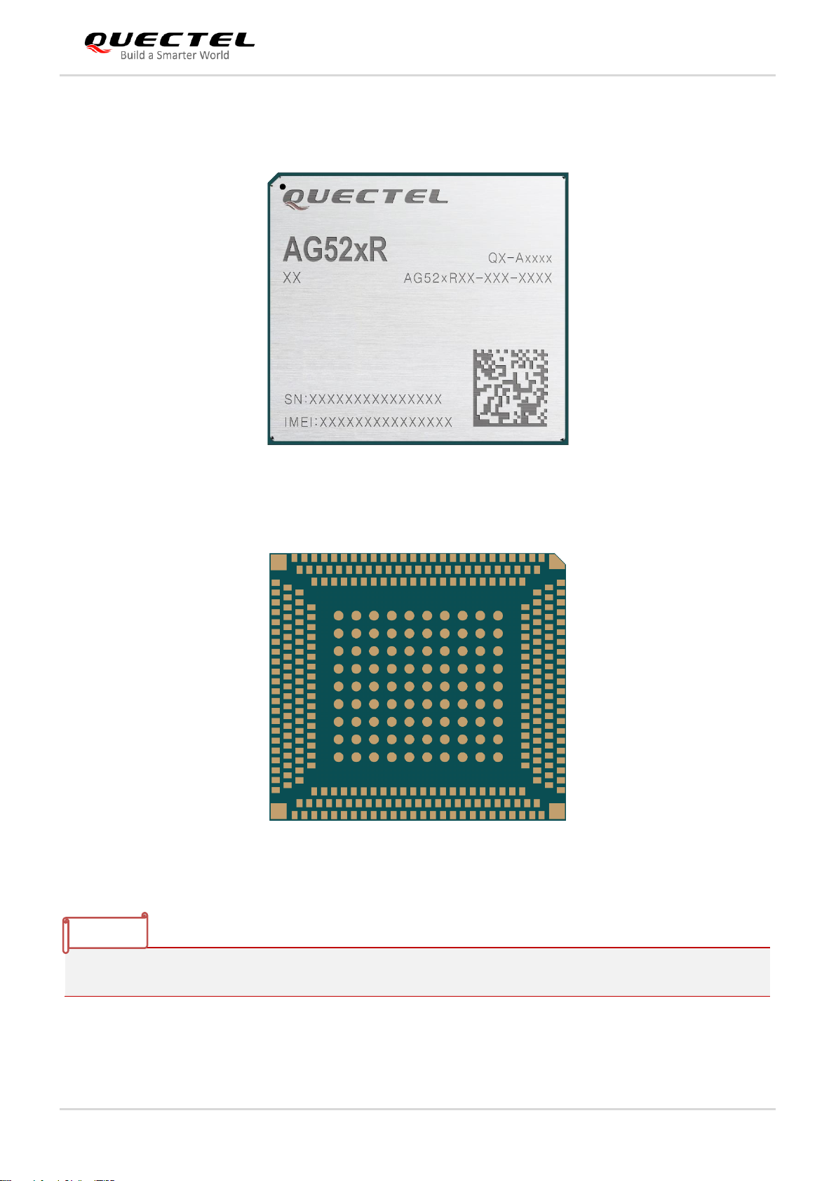
Automotive Module Series
AG521R-NA QuecOpen Hardware Design
AG521R-NA_QuecOpen_Hardware_Design 83 / 104
6.3. Top and Bottom Views
Figure 42: Top View of the Module
Figure 43: Bottom View of the Module
These are renderings of the module. For authentic appearance, see the module received from Quectel.
NOTE

Automotive Module Series
AG521R-NA QuecOpen Hardware Design
AG521R-NA_QuecOpen_Hardware_Design 84 / 104
7 Storage, Manufacturing and Packaging
7.1. Storage
The module is provided with vacuum-sealed packaging. MSL of the module is rated as 3. The storage requirements
are shown below.
1. Recommended Storage Condition: The temperature should be 23 ±5 °C and the relative humidity should be
35–60 %.
2. The storage life (in vacuum-sealed packaging) is 12 months in Recommended Storage Condition.
3. The floor life of the module is 168 hours
1)
in a plant where the temperature is 23 ±5 °C and relative humidity is
below 60 %. After the vacuum-sealed packaging is removed, the module must be processed in reflow soldering
or other high-temperature operations within 24 hours. Otherwise, the module should be stored in an
environment where the relative humidity is less than 10% (e.g. a drying cabinet).
4. The module should be pre-baked to avoid blistering, cracks and inner-layer separation in PCB under the
following circumstances:
⚫ The module is not stored in Recommended Storage Condition;
⚫ Violation of the third requirement above occurs;
⚫ Vacuum-sealed packaging is broken, or the packaging has been removed for over 24 hours;
⚫ Before module repairing.
5. If needed, the pre-baking should follow the requirements below:
⚫ The module should be baked for 8 hours at 120 ±5 °C;
⚫ All modules must be soldered to PCB within 24 hours after the baking, otherwise they should be put in a
dry environment such as in a drying oven.
NOTE

Automotive Module Series
AG521R-NA QuecOpen Hardware Design
AG521R-NA_QuecOpen_Hardware_Design 85 / 104
1.
1)
This floor life is only applicable when the environment conforms to IPC/JEDEC J-STD-033.
2. To avoid blistering, layer separation and other soldering issues, it is forbidden to expose the modules to the air
for a long time. It is recommended to start the solder reflow process within 24 hours after the package is
removed if the temperature and moisture do not conform to IPC/JEDEC J-STD-033. And do not remove the
packages of tremendous modules if they are not ready for soldering.
3. Please take the module out of the packaging and put it on high-temperature resistant fixtures before the baking.
If shorter baking time is desired, see IPC/JEDEC J-STD-033 for baking procedure.
7.2. Manufacturing and Soldering
Push the squeegee to apply the solder paste on the surface of stencil, thus making the paste fill the stencil openings
and then penetrate to the PCB. The force on the squeegee should be adjusted properly so as to produce a clean
stencil surface on a single pass. To ensure the module soldering quality, the thickness of stencil for the module is
recommended to be 0.15–0.18 mm. For more details, see document [6].
It is suggested that the peak reflow temperature is 238–246 ºC, and the absolute maximum reflow temperature is
246 ºC. To avoid damage to the module caused by repeated heating, it is strongly recommended that the module
should be mounted after reflow soldering for the other side of PCB has been completed. The recommended reflow
soldering thermal profile (lead-free reflow soldering) and related parameters are shown below.
Tem p. (°C )
R eflow Z one
S oak Z one
246
200
220
238
C
D
B
A
150
100
M ax slop e : 1~ 3 °C /s
C oolin g dow n slop e :
-1.5 ~ -3 °C /s
M ax slop e :
2~ 3 °C /s
Figure 44: Recommended Reflow Soldering Thermal Profile
Table 38: Recommended Thermal Profile Parameters

Automotive Module Series
AG521R-NA QuecOpen Hardware Design
AG521R-NA_QuecOpen_Hardware_Design 86 / 104
7.3. Packaging
The module is packaged in tape and reel carriers. One reel is 10.56 meters long and contains 220 modules. The
figures below show the packaging details, measured in mm.
Factor
Recommendation
Soak Zone
Max slope
1–3 °C/s
Soak time (between A and B: 150°C and 200°C)
70–120 s
Reflow Zone
Max slope
2–3 °C/s
Reflow time (D: over 220°C)
45–70 s
Max temperature
238–246 °C
Cooling down slope
-1.5 to -3 °C/s
Reflow Cycle
Max reflow cycle
1

Automotive Module Series
AG521R-NA QuecOpen Hardware Design
AG521R-NA_QuecOpen_Hardware_Design 87 / 104
Figure 45: Tape Specifications
Figure 46: Reel Specifications

Automotive Module Series
AG521R-NA QuecOpen Hardware Design
AG521R-NA_QuecOpen_Hardware_Design 88 / 104
8 Appendix A References
Table 39: Related Documents
SN
Document Name
Remark
[1]
Quectel_V2X&5G_EVB_User_Guide
EVB User Guide for Automotive Modules
[2]
Quectel_AG52xR_Series_QuecOpen_Developer_Guide
AG52xR Series QuecOpen Developer Guide
[3]
Quectel_AG52xR_Series _AT_Commands_Manual
AG52xR Series AT Commands Manual
[4]
Quectel_RF_Layout_Application_Note
RF Layout Application Note
[5]
Quectel_LTE_Module_Thermal_Design_Guide
Thermal Design Guide for Quectel LTE (LTE
Standard/LTE-A/Automotive) modules
[6]
Quectel_Module_Secondary_SMT_Application_Note
Quectel Module Secondary SMT Application
Note
[7]
Quectel_AG52xR_Series_QuecOpen_Reference_Design
AG52xR Series QuecOpen Reference Design
Table 40: Terms and Abbreviations
Abbreviation
Description
AMR
Adaptive Multi-rate
API
Application Program Interface
bps
Bits Per Second
BT
Bluetooth
CHAP
Challenge Handshake Authentication Protocol
CS
Coding Scheme
CSD
Circuit Switched Data
CTS
Clear To Send

Automotive Module Series
AG521R-NA QuecOpen Hardware Design
AG521R-NA_QuecOpen_Hardware_Design 89 / 104
DC-HSPA+
Dual-carrier High Speed Packet Access
DFOTA
Delta Firmware Upgrade Over The Air
DL
Downlink
DTR
Data Terminal Ready
DTX
Discontinuous Transmission
EFR
Enhanced Full Rate
ESD
Electrostatic Discharge
EVDO
Evolution-Data Optimized
FDD
Frequency Division Duplex
FR
Full Rate
GLONASS
GLObalnaya NAvigatsionnaya Sputnikovaya Sistema, the Russian Global
Navigation Satellite System
GMSK
Gaussian Minimum Shift Keying
GPS
Global Positioning System
GSM
Global System for Mobile Communications
HR
Half Rate
HSPA
High Speed Packet Access
HSDPA
High Speed Downlink Packet Access
HSUPA
High Speed Uplink Packet Access
I/O
Input/Output
Inorm
Normal Current
LED
Light Emitting Diode
LNA
Low Noise Amplifier
LTE
Long Term Evolution
MIMO
Multiple Input Multiple Output
MO
Mobile Originated

Automotive Module Series
AG521R-NA QuecOpen Hardware Design
AG521R-NA_QuecOpen_Hardware_Design 90 / 104
MS
Mobile Station (GSM engine)
MT
Mobile Terminated
PAP
Password Authentication Protocol
PCB
Printed Circuit Board
PDU
Protocol Data Unit
PPP
Point-to-Point Protocol
Ppp
Peak Pulse Power
QAM
Quadrature Amplitude Modulation
QPSK
Quadrature Phase Shift Keying
RF
Radio Frequency
RHCP
Right Hand Circularly Polarized
Rx
Receive
SIMO
Single Input Multiple Output
SMS
Short Message Service
TDD
Time Division Duplexing
TDMA
Time Division Multiple Access
TD-SCDMA
Time Division-Synchronous Code Division Multiple Access
TX
Transmitting Direction
UL
Uplink
UMTS
Universal Mobile Telecommunications System
URC
Unsolicited Result Code
(U)SIM
(Universal) Subscriber Identity Module
Vmax
Maximum Voltage Value
Vnorm
Normal Voltage Value
Vmin
Minimum Voltage Value

Automotive Module Series
AG521R-NA QuecOpen Hardware Design
AG521R-NA_QuecOpen_Hardware_Design 91 / 104
VIHmax
Maximum Input High Level Voltage Value
VIHmin
Minimum Input High Level Voltage Value
VILmax
Maximum Input Low Level Voltage Value
VILmin
Minimum Input Low Level Voltage Value
VImax
Absolute Maximum Input Voltage Value
VImin
Absolute Minimum Input Voltage Value
VOHmax
Maximum Output High Level Voltage Value
VOHmin
Minimum Output High Level Voltage Value
VOLmax
Maximum Output Low Level Voltage Value
VOLmin
Minimum Output Low Level Voltage Value
V
RWM
Reserve Stand-Off Voltage
VSWR
Voltage Standing Wave Ratio
WCDMA
Wideband Code Division Multiple Access
WLAN
Wireless Local Area Network

OEM/Integrators Installation Manual
Important Notice to OEM integrators 1. This module is limited to OEM installation ONLY. 2. This module
is limited to installation in mobile or fixed applications, according to Part 2.1091(b). 3. The separate
approval is required for all other operating configurations, including portable configurations with respect
to Part 2.1093 and different antenna configurations 4. For FCC Part 15.31 (h) and (k): The host
manufacturer is responsible for additional testing to verify compliance as a composite system. When
testing the host device for compliance with Part 15 Subpart B, the host manufacturer is required to show
compliance with Part 15 Subpart B while the transmitter module(s) are installed and operating. The
modules should be transmitting and the evaluation should confirm that the module's intentional
emissions are compliant (i.e. fundamental and out of band emissions). The host manufacturer must
verify that there are no additional unintentional emissions other than what is permitted in Part 15 Subpart
B or emissions are complaint with the transmitter(s) rule(s). The Grantee will provide guidance to the
host manufacturer for Part 15 B requirements if needed.
Important Note
notice that any deviation(s) from the defined parameters of the antenna trace, as described by the
instructions, require that the host product manufacturer must notify to Quectel that they wish to change
the antenna trace design. In this case, a Class II permissive change application is required to be filed by
the USI, or the host manufacturer can take responsibility through the change in FCC ID (new application)
procedure followed by a Class II permissive change application
End Product Labeling
When the module is installed in the host device, the FCC/IC ID label must be visible through a window
on the final device or it must be visible when an access panel, door or cover is easily re-moved. If not, a
second label must be placed on the outside of the final device that contains the following text: “Contains
FCC ID: XMR2021AG521RNA” “Contains IC: XMR2021AG521RNA”. The FCC ID/IC ID can be used
only when all FCC/IC compliance requirements are met.

Antenna
(1) The antenna must be installed such that 20 cm is maintained between the antenna and users,
(2) The transmitter module may not be co-located with any other transmitter or antenna.
In the event that these conditions cannot be met (for example certain laptop configurations or co-location
with another transmitter), then the FCC/IC authorization is no longer considered valid and the FCC ID/IC
ID cannot be used on the final product. In these circumstances, the OEM integrator will be responsible
for re-evaluating the end product (including the transmitter) and obtaining a separate FCC/IC
authorization.
To comply with FCC regulations limiting both maximum RF output power and human exposure to RF
radiation, maximum antenna gain (including cable loss) must not exceed
Test Mode
Antenna Gain (dBi)
Test Mode
Antenna Gain (dBi)
WCDMA B2
8.00
LTE B12
5.00
WCDMA B4
8.00
LTE B13
5.00
WCDMA B5
5.00
LTE B14
5.00
LTE B2
8.00
LTE B25
8.00
LTE B4
8.00
LTE B26
5.00
LTE B5
5.00
LTE B66
5.00
LTE B7
8.00
LTE B71
5.00
Note: “*” means when using maximum gain antenna, the host manufacturer should reduce the
conducted power to meet the FCC maximum RF output power limit.
Manual Information to the End User
The OEM integrator has to be aware not to provide information to the end user regarding how to install
or remove this RF module in the user’s manual of the end product which integrates this module. The end
user manual shall include all required regulatory information/warning as show in this manual

Federal Communication Commission Interference Statement
This device complies with Part 15 of the FCC Rules. Operation is subject to the following two conditions:
(1) This device may not cause harmful interference, and (2) this device must accept any interference
received, including interference that may cause undesired operation.
This equipment has been tested and found to comply with the limits for a Class B digital device, pursuant
to Part 15 of the FCC Rules. These limits are designed to provide reasonable protection against harmful
interference in a residential installation. This equipment generates, uses and can radiate radio frequency
energy and, if not installed and used in accordance with the instructions, may cause harmful interference
to radio communications. However, there is no guarantee that interference will not occur in a particular
installation. If this equipment does cause harmful interference to radio or television reception, which can
be determined by turning the equipment off and on, the user is encouraged to try to correct the
interference by one of the following measures:
- Reorient or relocate the receiving antenna.
- Increase the separation between the equipment and receiver
- Connect the equipment into an outlet on a circuit different from that to which the receiver is connected.
- Consult the dealer or an experienced radio/TV technician for help.
Any changes or modifications not expressly approved by the party responsible for compliance could void
the user's authority to operate this equipment. This transmitter must not be co-located or operating in
conjunction with any other antenna or transmitter.
List of applicable FCC rules
This module has been tested and found to comply with part 22, part 24, part 27, part 90 requirements for
Modular Approval.
The modular transmitter is only FCC authorized for the specific rule parts (i.e., FCC transmitter rules)
listed on the grant, and that the host product manufacturer is responsible for compliance to any other
FCC rules that apply to the host not covered by the modular transmitter grant of certification. If the
grantee markets their product as being Part 15 Subpart B compliant (when it also contains unintentional-
radiator digital circuity), then the grantee shall provide a notice stating that the final host product still
requires Part 15 Subpart B compliance testing with the modular transmitter installed.

This device is intended only for OEM integrators under the following
conditions: (For module device use)
1) The antenna must be installed such that 20 cm is maintained between the antenna and users, and
2) The transmitter module may not be co-located with any other transmitter or antenna.
As long as 2 conditions above are met, further transmitter test will not be required. However, the OEM
integrator is still responsible for testing their end-product for any additional compliance requirements
required with this module installed.
Radiation Exposure Statement
This equipment complies with FCC radiation exposure limits set forth for an uncontrolled environment.
This equipment should be installed and operated with minimum distance 20 cm between the radiator &
your body.

Industry Canada Statement
This device complies with Industry Canada’s licence-exempt RSSs. Operation is subject to the following
two conditions:
(1) This device may not cause interference; and
(2) This device must accept any interference, including interference that may cause undesired operation
of the device.
Le présent appareil est conforme aux CNR d'Industrie Canada applicables aux appareils radio exempts
de licence. L'exploitation est autorisée aux deux conditions suivantes:
(1) l'appareil ne doit pas produire de brouillage, et
(2) l'utilisateur de l'appareil doit accepter tout brouillage radioélectrique subi, même si le brouillage est
susceptible d'en compromettre le fonctionnement."
Radiation Exposure Statement
This equipment complies with IC radiation exposure limits set forth for an uncontrolled environment. This
equipment should be installed and operated with minimum distance 20 cm between the radiator & your
body
Déclaration d'exposition aux radiations:
Cet équipement est conforme aux limites d'exposition aux rayonnements ISED établies pour un
environnement non contrôlé. Cet équipement doit être installé et utilisé avec un minimum de 20 cm de
distance entre la source de rayonnement et votre corps.
This device is intended only for OEM integrators under the following
conditions: (For module device use)
1) The antenna must be installed such that 20 cm is maintained between the antenna and users, and
2) The transmitter module may not be co-located with any other transmitter or antenna. As long as 2
conditions above are met, further transmitter test will not be required. However, the OEM integrator is still
responsible for testing their end-product for any additional compliance requirements required with this
module installed.

Cet appareil est conçu uniquement pour les intégrateurs OEM dans les
conditions suivantes: (Pour utilisation de dispositif module)
1) L'antenne doit être installée de telle sorte qu'une distance de 20 cm est respectée entre l'antenne et
les utilisateurs, et
2) Le module émetteur peut ne pas être coïmplanté avec un autre émetteur ou antenne.
Tant que les 2 conditions ci-dessus sont remplies, des essais supplémentaires sur l'émetteur ne seront
pas nécessaires. Toutefois, l'intégrateur OEM est toujours responsable des essais sur son produit final
pour toutes exigences de conformité supplémentaires requis pour ce module installé.
IMPORTANT NOTE:
In the event that these conditions cannot be met (for example certain laptop configurations or colocation
with another transmitter), then the Canada authorization is no longer considered valid and the IC ID
cannot be used on the final product. In these circumstances, the OEM integrator will be responsible for
re-evaluating the end product (including the transmitter) and obtaining a separate Canada authorization.
NOTE IMPORTANTE:
Dans le cas où ces conditions ne peuvent être satisfaites (par exemple pour certaines configurations
d'ordinateur portable ou de certaines co-localisation avec un autre émetteur), l'autorisation du Canada
n'est plus considéré comme valide et l'ID IC ne peut pas être utilisé sur le produit final. Dans ces
circonstances, l'intégrateur OEM sera chargé de réévaluer le produit final (y compris l'émetteur) et
l'obtention d'une autorisation distincte au Canada.
End Product Labeling
This transmitter module is authorized only for use in device where the antenna may be installed such
that 20 cm may be maintained between the antenna and users. The final end product must be labeled in
a visible area with the following: “Contains IC: 10224A-2021AG521R”.
Plaque signalétique du produit final
Ce module émetteur est autorisé uniquement pour une utilisation dans un dispositif où l'antenne peut
être installée de telle sorte qu'une distance de 20cm peut être maintenue entre l'antenne et les
utilisateurs. Le produit final doit être étiqueté dans un endroit visible avec l'inscription suivante: "Contient
des IC: 10224A-2021AG521R".

Manual Information to the End User
The OEM integrator has to be aware not to provide information to the end user regarding how to install
or remove this RF module in the user’s manual of the end product which integrates this module.
The end user manual shall include all required regulatory information/warning as show in this manual.
Manuel d'information à l'utilisateur final
L'intégrateur OEM doit être conscient de ne pas fournir des informations à l'utilisateur final quant à la
façon d'installer ou de supprimer ce module RF dans le manuel de l'utilisateur du produit final qui intègre
ce module.
Le manuel de l'utilisateur final doit inclure toutes les informations réglementaires requises et
avertissements comme indiqué dans ce manuel.
 Loading...