

lQ QT60160, QT60240
16
AND
24 KEY QM
ATRIX
™ T
OUCH SENSOR
IC
s
/RST
Y2A
Y1A
Y0A
SDA
SCL
These devices are designed for low cost mobile and consumer electronics
applications.
QMatrix™ technology employs transverse charge-transfer sensing electrode
designs which can be made very compact and are easily wired. Charge is
forced from an emitting electrode into the overlying panel dielectric, and then
collected on a receiver electrode which directs the charge into a sampling
capacitor which is then converted directly to digital form without the use of
amplifiers.
Keys are configured in a matrix format that minimizes the number of required
scan lines and device pins. The key electrodes can be designed into a
conventional Printed Circuit Board (PCB) or Flexible Printed Circuit Board
(FPCB) as a copper pattern, or as printed conductive ink on plastic film.
M_SYNC
CHANGE
VSS
VDD
VSS
VDD
32
2
3
4
5
6
X6
7
X7 X5
817
910
LATCH
29 282726
QT60240
QT60160
MLF-32
13
11
12
VREF
S_SYNCX0X1X2X3
14
31 30
AT A GLANCE
Number of keys: 1 to 16 (QT60160), or 1 to 24 (QT60240)
Technology: Patented spread-spectrum charge-transfer (transverse mode)
Key outline sizes: 6mm x 6mm or larger (panel thickness dependent); widely different sizes and shapes possible
Key spacings: 8mm or wider, center to center (panel thickness dependent)
Electrode design: Two-part electrode shapes (drive-receive); wide variety of possible layouts
Layers required: One layer (with jumpers), two layers (no jumpers)
†
Electrode materials: PCB, FPCB, silver or carbon on film, ITO on film, Orgacon
Panel materials: Plastic, glass, composites, painted surfaces (low particle density metallic paints possible)
Adjacent Metal: Compatible with grounded metal immediately next to keys
Panel thickness: Up to 50mm glass, 20mm plastic (key size dependent)
Key sensitivity: Individually settable via simple commands over serial interface
2
Interface: I
C slave mode (100kHz), or parallel output via external shift registers
Moisture tolerance: Best in class.
Power: 1.8V ~ 5.5V, 40µA (16 keys at 1.8V, 2s Low Power mode). Guaranteed to 1.62V.
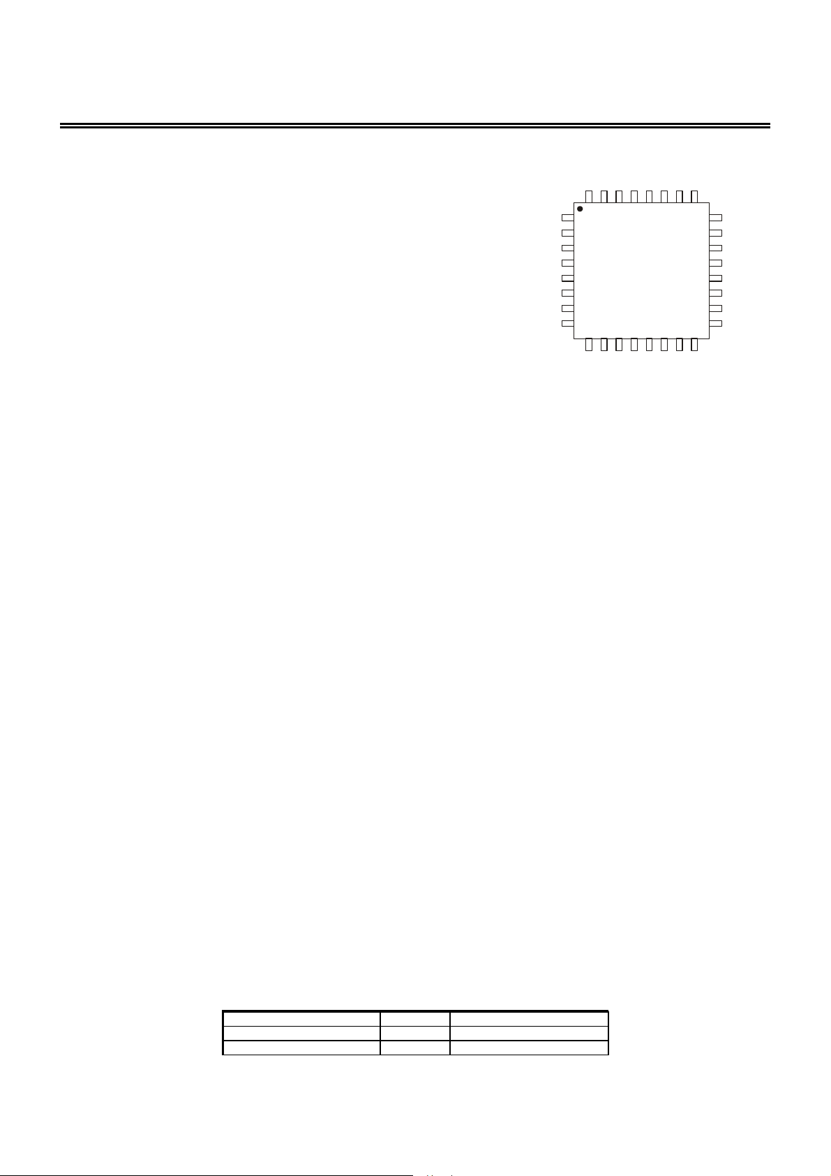
Package: 32-pin 5 x 5mm MLF RoHS compliant
Signal processing: Self-calibration, auto drift compensation, noise filtering, Adjacent Key Suppression
Applications: Mobile phones, remote controls, domestic appliances, PC peripherals, automotive
ink on film
TM
SMP
25
1615
Y2B
X4
24
23
22
21
20
19
18
Y1B1
Y0B
A0
VSS
VDD
A1
VDD
†
Orgacon is a registered trademark of Agfa-Gevaert N.V
LQ
AVAILABLE OPTIONS
KeysPart Number
-40
-400C to +850C24QT60240-ISG
T
A
0
C to +850C16QT60160-ISG
Copyright © 2006 QRG Ltd
QT60240-ISG R8.06/0906

Contents
1 Overview
1.1 Introduction
1.2 Part Differences
1.3 Enabling / Disabling Keys
2 Hardware and Functional
2.1 Matrix Scan Sequence
2.2 Burst Paring
2.3 Cs Sample Capacitor Operation
2.4 Sample Capacitor Saturation
2.5 Sample Resistors
2.6 Signal Levels
2.7 Matrix Series Resistors
2.8 Key Design
2.9 PCB Layout, Construction
2.10 Power Supply Considerations
2.11 Startup / Calibration Times
2.12 Reset Input
2.13 Spread Spectrum Acquisitions
2.14 Detection Integrators
2.15 Sleep
2.16 Wiring
3 Interfaces
3.1 Introduction
3.2 Shift Register Output Mode
3.3 I2C Port
3.4 CHANGE Pin
4 Control Commands
4.1 Introduction
4.2 Writing Data to the Device
4.3 Reading Data From the Device
4.4 Report Detections for All Keys
4.5 Raw Data Commands
4.6 Cal All
4.7 Setups
...............................
............................
..........................
............................
.........................
...........................
............................
2.9.1 Overview
2.9.2 LED Traces and Other Switching Signals
2.9.3 PCB Cleanliness
...........................
........................
...........................
..............................
..............................
..............................
............................
..............................
...........................
........................
............................
...............................
..............................
.....................
.....................
.......................
..................
...................
......................
.....................
..............
..................
....................
..................
.......................
....................
.....................
..................
...................
.......................
5 I2C Operation
3
5.1 Interface Bus
3
5.2 Transferring Data Bits
3
5.3 START and STOP Conditions
3
5.4 Address Packet Format
3
5.5 Data Packet Format
3
5.6 Combining Address and Data Packets Into a Transmission
3
6 Setups
3
6.1 Introduction
4
6.2 Negative Threshold - NTHR
4
6.3 Positive Threshold - PTHR
4
6.4 Drift Compensation - NDRIFT, PDRIFT
5
6.5 Detect Integrators - NDIL, FDIL
6
6.6 Negative Recal Delay - NRD
6
6.7 Positive Recalibration Delay - PRD
6
6.8 Burst Length - BL
6
6.9 Adjacent Key Suppression - AKS
6
6.10 Oscilloscope Sync - SSYNC
6
6.11 Mains Sync - MSYNC
7
6.12 Sleep Duration - SLEEP
7
6.13 Wake on Key Touch - WAKE
7
6.14 Awake Timeout - AWAKE
7
6.15 Drift Hold Time - DHT
7
6.16 Setups Block
8
7 Specifications
10
10
10
10
11
12
12
12
12
12
13
13
13
7.1 Absolute Maximum Electrical Specifications
7.2 Recommended Operating Conditions
7.3 DC Specifications
7.4 Timing Specifications
7.5 Power Consumption
7.6 Mechanical Dimensions
7.7 Marking
7.8 Moisture Sensitivity Level (MSL)
............................
...........................
.......................
...................
......................
........................
....
................................
............................
....................
....................
..............
..................
....................
................
.........................
.................
...................
......................
.....................
...................
....................
......................
..........................
...........................
............
...............
.........................
.......................
........................
......................
..............................
..................
15
15
15
15
15
15
16
17
17
17
17
17
18
18
18
19
19
19
19
20
20
20
20
21
23
23
23
23
23
24
25
25
25
lQ
2 QT60240-ISG R8.06/0906
1 Overvie
w
1.1 Introduction
QT60xx0 devices are digital burst mode charge-transfer (QT)
sensors designed specifically for matrix layout touch controls;
they include all signal processing functions necessary to
provide stable sensing under a wide variety of changing
conditions. Only a few external parts are required for
operation. The entire circuit can be built within a few square
centimeters of single-sided PCB area. CEM-1 and FR1
punched, single-sided materials can be used for the lowest
possible cost. The PCB’s rear can be mounted flush on the
back of a glass or plastic panel using a conventional
adhesive, such as 3M VHB two-sided adhesive acrylic film.
1.3 Enabling / Disabling Keys
The NDIL parameter is used to enable and disable keys in the
matrix. Setting NDIL = 0 for a key disables it (Section 6.5). At
no time can the number of enabled keys exceed the
maximum specified for the device (see Section 1.2).
On the QT60160, only the first 2 Y lines (Y0, Y1) are
operational by default. On the QT60160, to use keys located
on line Y2, one or more of the pre-enabled keys must be
disabled simultaneously while enabling the desired new keys.
This can be done in one Setups block load operation.
2 Hardware and Functional
Figure 1.1 Field Flow Between X and Y Elements
overlying panel
X
element
QT60xx0 devices employ transverse charge-transfer ('QT')
sensing, a technology that senses changes in electrical
charge forced across two electrode elements by a pulse edge
(Figure 1.1). QT60xx0 devices allow a wide range of key sizes
and shapes to be mixed together in a single touch panel.
The devices use an I
extracted and to permit individual key parameter setup. The
command structure is designed to minimize the amount of
data traffic while maximizing the amount of information
conveyed.
In addition to normal operating and setup functions the device
can also report back actual signal strengths.
QmBtn™ software for the PC can be used to program the
operation of the IC, as well as read back key status and
signal levels in real time.
2
C interface to allow key data to be
Y
elem ent
2.1 Matrix Scan Sequence
The circuit operates by scanning each key sequentially, key
by key. Key scanning begins with location X=0 / Y=0 (key 0).
X axis keys are known as rows while Y axis keys are referred
to as columns although this has no reflection on actual wiring .
Keys are scanned sequentially by row, for example the
sequence X0Y0 X1Y0 .... X7Y0, X0Y1, X1Y1... etc. Keys are
also numbered from 0...23. Key 0 is located at X0Y0.
Table 2.1 shows the key numbering.
Table 2.1 Key Numbers
X0X1X2X3X4X5X6X7
Y0
Y1
Y2
Each key is sampled in a burst of acquisition pulses whose
length is determined by the Setups parameter BL (page 19);
this can be set on a per-key basis. A burst is completed
entirely before the next key is sampled; at the end of each
burst the resulting signal is converted to digital form and
processed. The burst length directly impacts key gain; each
key can have a unique burst length in order to allow tailoring
of key sensitivity on a key-by-key basis.
01234567
89101112131415
Key
1617181920212223
numbers
2.2 Burst Paring
Keys that are disabled by setting NDIL = 0 (Section 6.5,
page 18) have their bursts removed from the scan sequence
to save scan time. As a consequence, the fewer keys that are
used the faster the device can respond. All calibration times
are reduced when keys
are
disabled
.
1.2 Part Differences
There are two versions of the device; one is capable of a
maximum of 16 keys (QT60160), the other is capable of a
maximum of 24 keys (QT60240).
These devices are identical in all respects, except for the
maximum number of keys specified. The keys can be located
anywhere within an electrical grid of 8 X and 3 Y scan lines.
Unused keys are always pared from the burst sequence in
order to optimize speed. Similarly, in a given part a lesser
number of enabled keys will cause any unused acquisition
burst timeslots to be pared from the sampling sequence to
optimize acquire speed. Thus, if only 14 keys are actually
enabled, only 14 timeslots are used for scanning.
lQ
2.3 Cs Sample Capacitor Operation
Cs capacitors absorb charge from the key electrodes on the
rising edge of each X pulse. On each falling edge of X, the Y
matrix line is clamped to ground to allow the electrode and
wiring charges to neutralize in preparation for the next pulse.
With each X pulse charge accumulates on Cs causing a
staircase increase in its differential voltage.
After the burst completes, the device clamps the Y line to
ground causing the opposite terminal to go negative. The
charge on Cs is then measured using an external resistor to
ramp the negative terminal upwards until a zero crossing is
achieved. The time required to zero cross becomes the
measurement result.
3 QT60240-ISG R8.06/0906
The Cs should be connected as shown in Figure 2.7, page 9.
The value of these capacitors is not critical but 4.7nF is
recommended for most cases. They should be 10 percent
X7R ceramics. If the transverse capacitive coupling from X to
Y is large enough the voltage on a Cs capacitor can saturate,
destroying gain. In such cases the burst length should be
reduced and/or the Cs value increased. See Section 2.4.
If a Y line is not used its corresponding Cs capacitor may be
omitted and the pins left floating.
2.4 Sample Capacitor Saturation
Cs voltage saturation at a pin YnB is shown in Figure 2.1
Saturation begins to occur when the voltage at a YnB pin
becomes more negative than -0.25V at the end of the burst.
This nonlinearity is caused by excessive voltage
accumulation on Cs inducing conduction in the pin protection
diodes. This badly saturated signal destroys key gain and
introduces a strong thermal coefficient which can cause
'phantom' detection. The cause of this is either from the burst
length being too long, the Cs value being too small, or the
X-Y transfer coupling being too large. Solutions include
loosening up the key structure interleaving, more separation
of the X and Y lines on the PCB, increasing Cs, and
decreasing the burst length.
Increasing Cs will make the part slower; decreasing burst
length will make it less sensitive. A better PCB layout and a
looser key structure (up to a point) have no negative effects.
Cs voltages should be observed on an oscilloscope with the
matrix layer bonded to the panel material; if the Rs side of
any Cs ramps more negative than -0.25 volts during any burst
(not counting overshoot spikes which are probe artifacts),
there is a potential saturation problem.
Figure 2.2 shows a defective waveform similar to that of 2.1,
but in this case the distortion is caused by excessive stray
capacitance coupling from the Y line to AC ground; for
example, from running too near and too far alongside a
ground trace, ground plane, or other traces. The excess
coupling causes the charge-transfer effect to dissipate a
significant portion of the received charge from a key into the
stray capacitance. This phenomenon is more subtle; it can be
best detected by increasing BL to a high count and watching
what the waveform does as it descends towards and below
-0.25V. The waveform will appear deceptively straight, but it
will slowly start to flatten even before the -0.25V level is
reached.
A correct waveform is shown in Figure 2.3. Note that the
bottom edge of the bottom trace is substantially straight
(ignoring the downward spikes).
Unlike other QT circuits, the Cs capacitor values on QT60xx0
devices have no effect on conversion gain. However, they do
affect conversion time.
Unused Y lines should be left open.
2.5 Sample Resistors
There are three sample resistors (Rs) used to perform
single-slope ADC conversion of the acquired charge on each
Cs capacitor. These resistors directly control acquisition gain;
larger values of Rs will proportionately increase signal gain.
For most applications Rs should be 1M✡. Unused Y lines do
not require an Rs resistor.
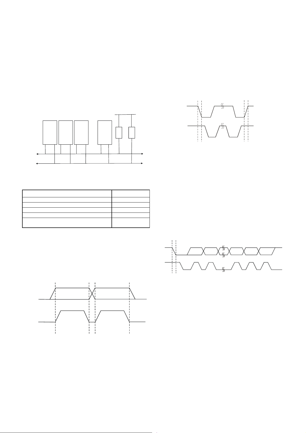
Figure 2.1 VCs - Nonlinear During Burst
(Burst too long, or Cs too small, or X-Y transcapacitance too large)
X Drive
YnB
Figure 2.2 VCs - Poor Gain, Nonlinear During Burst
(Excess capacitance from Y line to Gnd)
X Drive
YnB
Figure 2.3 VCs - Correct
X Drive
YnB
Figure 2.4 X-Drive Pulse Roll-off and Dwell Time
The Dwell time is fixed at ~500ns - see Section 2.7
X drive
Dwell time
Y gate
Lost charge due to
inadequate settling
before end of dwell time
2.6 Signal Levels
Quantum’s QmBtn software makes it is easy to observe the
absolute level of signal received by the sensor on each key.
The signal values should normally be in the range of 200 to
750 counts with properly designed key shapes and values of
Rs. However, long adjacent runs of X and Y lines can also
artificially boost the signal values, and induce signal
saturation; this is to be avoided. The X-to-Y coupling should
come mostly from intra-key electrode coupling, not from stray
X-to-Y trace coupling.
lQ
4 QT60240-ISG R8.06/0906
Figure 2.5 Probing X-Drive
Waveforms With a Coin
Figure 2.6 Recommended Key Structure
‘T’ should ideally be similar to the complete thickness the fields
need to penetrate to the touch surface. Sm aller dimens ions will also
work but will give less signal strength. If in doubt, make the pattern
coarser. The lower figure shows a simpler structure used for
compact key layouts, for exam ple for m obile phones. A layout with a
common X drive and three receive electrodes is depicted.
Y0
QmBtn software is available free of charge on Quantum’s
website www.qprox.com.
The signal swing from the smallest finger touch should
preferably exceed 8 counts, with 12 being a reasonable
target. The signal threshold setting (NTHR) should be set to a
value guaranteed to be less than the signal swing caused by
the smallest touch.
Increasing the burst length (BL) parameter will increase the
signal strengths as will increasing the sampling resistor (Rs)
values.
2.7 Matrix Series Resistors
The X and Y matrix scan lines can use series resistors
(referred to as Rx and Ry respectively) for improved EMC
performance (Figure 2.7, page 9).
X drive lines require Rx in most cases to reduce edge rates
and thus reduce RF emissions. Typical values range from
1K
✡
to 20K✡.
Y lines need Ry to reduce EMC susceptibility problems and in
some extreme cases, ESD. Typical Y values are about 1K
Y resistors act to reduce noise susceptibility problems by
forming a natural low-pass filter with the Cs capacitors.
It is essential that the Rx and Ry resistors and Cs capacitors
be placed very close to the chip. Placing these parts more
than a few millimeters away opens the circuit up to high
frequency interference problems (above 20MHz) as the trace
lengths between the components and the chip start to act as
RF antennae.
✡
X0
Y1
Y2
The upper limits of Rx and Ry are reached when the signal
level and hence key sensitivity are clearly reduced. The limits
of Rx and Ry will depend on key geometry and stray
capacitance, and thus an oscilloscope is required to
determine optimum values of both.
Dwell time is the duration in which charge coupled from X to
Y is captured (Figure 2.4, page 4). Increasing Rx values will
cause the leading edge of the X pulses to increasingly roll off,
causing the loss of captured charge (and hence loss of signal
.
strength) from the keys.
The dwell time of these parts is fixed at 500ns. If the X pulses
have not settled within 500ns, key gain will be reduced; if this
happens, either the stray capacitance on the X line(s) should
be reduced (by a layout change, for example by reducing X
line exposure to nearby ground planes or traces), or, the Rx
resistor needs to be reduced in value (or a combination of
both approaches).
lQ
5 QT60240-ISG R8.06/0906

One way to determine X line settling time is to monitor the
fields using a patch of metal foil or a small coin over the key
(Figure 2.5). Only one key along a particular X line needs to
be observed, as each of the keys along that X line will be
identical. The 500ns dwell time should exceed the observed
95 percent settling of the X-pulse by 25 percent or more.
In almost all cases, Ry should be set equal to Rx, which will
ensure that the charge on the Y line is fully captured into the
Cs capacitor.
2.8 Key Design
Circuits can be constructed out of a variety of materials
including conventional FR-4, Flexible Printed Circuit Boards
(FPCB), silver silk-screened on PET plastic film, and even
inexpensive punched single-sided CEM-1 and FR-2.
The actual internal pattern style is not as important as the
need to achieve regular X and Y widths and spacings of
sufficient size to cover the desired graphical key area or a
little bit more; ~3mm oversize is acceptable in most cases,
since the key’s electric fields drop off near the edges anyway.
The overall key size can range from 6mm x 6mm up to
100mm x 100mm but these are not hard limits. The keys can
be any shape including round, rectangular, square, etc. The
internal pattern can be interdigitated as shown in Figure 2.6.
For small, dense keypads, electrodes such as shown in the
lower half of Figure 2.6 can be used. Where the panels are
thin (usually mobile phones have panels under 2mm thick)
the electrode density can be quite high.
For better surface moisture suppression, the outer perimeter
of X should be as wide as possible, and there should be no
ground planes near the keys. The variable ‘T’ in this drawing
represents the total thickness of all materials that the keys
must penetrate.
2.9 PCB Layout, Construction
Ground planes, if used, should be placed under or around the
QT chip itself and the associated resistors and capacitors in
the circuit, under or around the power supply, and back to a
connector, but nowhere else.
2.9.2 LED Traces and Other Switching Signals
Digital switching signals near the Y lines will induce transients
into the acquired signals, deteriorating the SNR perfomance
of the device. Such signals should be routed away from the Y
lines, or the design should be such that these lines are not
switched during the course of signal acquisition (bursts).
LED terminals which are multiplexed or switched into a
floating state and which are within or physically very near a
key structure (even if on another nearby PCB) should be
bypassed to either Vss or Vdd with at least a 10nF capacitor
to suppress capacitive coupling effects which can induce
false signal shifts. The bypass capacitor does not need to be
next to the LED, in fact it can be quite distant. The bypass
capacitor is noncritical and can be of any type.
LED terminals which are constantly connected to Vss or Vdd
do not need further bypassing.
2.9.3 PCB Cleanliness
All capacitive sensors should be treated as highly sensitive
circuits which can be influenced by stray conductive leakage
paths. QT devices have a basic resolution in the femtofarad
range; in this region, there is no such thing as ‘no clean flux’.
Flux absorbs moisture and becomes conductive between
solder joints, causing signal drift and resultant false
detections or transient losses of sensitivity or instability.
Conformal coatings will trap in existing amounts of moisture
which will then become highly temperature sensitive.
The designer should specify ultrasonic cleaning as part of the
manufacturing process, and in cases where a high level of
humidity is anticipated, the use of conformal coatings after
cleaning to keep out moisture.
2.9.1 Overview
It is best to place the chip near the touch keys on the same
PCB so as to reduce X and Y trace lengths, thereby reducing
the chances for EMC problems. Long connection traces act
as RF antennae. The Y (receive) lines are much more
susceptible to noise pickup than the X (drive) lines.
Even more importantly, all signal related discrete parts
(resistors and capacitors) should be very close to the body of
the chip. Wiring between the chip and the various resistors
and capacitors should be as short and direct as possible to
suppress noise pickup.
Ground planes and traces should NOT
be used around the keys and the Y lines
from the keys. Ground areas, traces, and
other adjacent signal conductors that act
as AC ground (such as Vdd and LED drive
lines etc.) will absorb the received key signals and
reduce signal-to-noise ratio (SNR) and thus will be
counterproductive. Ground planes around keys will also
make water film effects worse.
2.10 Power Supply Considerations
The power supply can range from +1.8V to +5V nominal. The
device can tolerate ±5mV/s short-term power supply
fluctuations. If the power supply fluctuates slowly with
temperature, the device will track and compensate for these
changes automatically with only minor changes in sensitivity.
If the supply voltage drifts or shifts quickly, the drift
compensation mechanism will not be able to keep up,
causing sensitivity anomalies or false detections.
As these devices use the power supply itself as an analog
reference, the power should be very clean and come from a
separate regulator. A standard inexpensive Low Dropout
(LDO) type regulator should be used that is not also used to
power other loads such as LEDs, relays, or other high current
devices. Load shifts on the output of the LDO can cause Vdd
to fluctuate enough to cause false detection or sensitivity
shifts.
Caution: A regulator IC shared with other logic can result in
erratic operation and is not advised.
A regulator can be shared among two or more QT devices on
one board. One such regulator known to work well with QT
chips is the S-817 series from Seiko Instruments
(Seiko Instruments - www.sii-ic.com).
lQ
6 QT60240-ISG R8.06/0906

A single ceramic 0.1uF bypass capacitor, with short traces,
should be placed very close to supply pins 3, 4, 5 and 6 of the
IC. Failure to do so can result in device oscillation, high
current consumption, erratic operation etc. Pins 18, 20, and
21 do not require bypassing.
2.11 Startup / Calibration Times
The devices require initialization times of up to 20ms. A
calibration takes one matrix scan.
Disabled keys are subtracted from the burst sequence and
thus the cal time is shortened. The scan time should be
measured on an oscilloscope.
2.12 Reset Input
The /RST pin can be used to reset the device to simulate a
power-down cycle, in order to bring the device up into a
known state should communications with the device be lost.
The pin is active low, and a low pulse lasting at least 10µs
must be applied to this pin to cause a reset.
The reset pin has an internal 30K
capacitor plus a diode to Vdd can be connected to this pin as
a traditional reset circuit, but this is not required.
If an external hardware reset is not used, the reset pin may
be connected to Vdd or left floating.
✡
- 60K✡ resistor. A 2.2µF
The QT60xx0 uses a two-tier confirmation mechanism having
two such counters for each key. These can be thought of as
‘inner loop’ and ‘outer loop’ confirmation counters.
The ‘inner’ counter is referred to as the ‘fast-DI’; this acts to
attempt to confirm a detection via rapid successive
acquisition bursts, at the expense of delaying the sampling of
the next key. Each key has its own fast-DI counter and limit
value; these limits can be changed via the Setups block on a
per-key basis.
The ‘outer’ counter is referred to as the ‘normal-DI’; this DI
counter increments whenever the fast-DI counter has reached
its limit value. If a fast-DI counter failed to reach its terminal
count, the corresponding normal-DI counter is also reset. The
normal-DI counter also has a limit value which is settable on
a per-key basis. If a normal-DI counter reaches its terminal
count, the corresponding key is declared to be touched and
becomes ‘active’. Note that the normal-DI can only be
incremented once per complete keyscan cycle, i.e. more
slowly, whereas the fast-DI is incremented ‘on the spot’
without interruption.
The net effect of this mechanism is a multiplication of the
inner and outer counters and hence a highly noise-resistance
sensing method. If the inner limit is set to 5, and the outer to
3, the net effect is 5x3=15 successive threshold crossings to
declare a key as active.
2.13 Spread Spectrum Acquisitions
QT60xx0 devices use spread-spectrum burst modulation.
This has the effect of drastically reducing the possibility of
EMI effects on the sensor keys, while simultaneously
spreading RF emissions. This feature is hard-wired into the
device and cannot be disabled or modified.
Spread spectrum is configured as a frequency chirp over a
wide range of frequencies for robust operation.
2.14 Detection Integrators
See also Section 6.5, page 18.
The devices feature a detection integration mechanism, which
acts to confirm a detection in a robust fashion. A per-key
counter is incremented each time the key has exceeded its
threshold and stayed there for a number of acquisitions.
When this counter reaches a preset limit the key is finally
declared to be touched.
For example, if the limit value is 10, then the device has to
exceed its threshold and stay there for 10 acquisitions in
succession without going below the threshold level, before
the key is declared to be touched. If on any acquisition the
signal is not seen to exceed the threshold level, the counter is
cleared and the process has to start from the beginning.
2.15 Sleep
The device will sleep whenever possible to conserve power.
Periodically, the part will wake automatically, scan the matrix,
and return to sleep unless there is activity which demands
further attention. The part will always return to sleep
automatically once all activity has ceased. The time for which
the part will sleep before automatically awakening can be
configured.
A new communication with the device while it is asleep will
cause it to wake up, service the communication and scan the
matrix. At least one full matrix scan is always performed after
waking up and before returning to sleep.
At the end of each matrix scan, the part will return to sleep
unless recent activity demands further attention. If there has
been recent activity, the part will perform another complete
matrix scan and then attempt to sleep once again. This
process is repeated indefinitely until the activity stops and the
part returns to sleep.
Key touch activity will prevent the part from sleeping. The part
will not sleep if any touch events were detected at any key in
the most recent scan of the key matrix.
lQ
7 QT60240-ISG R8.06/0906

2.16 Wiring
Table 2.2 Pin Listing
If Unused, Connect To...CommentsI/OFunctionPin
VddMains Sync inputIM_SYNC1
Leave openState change notification OCHANGE2
-Supply groundPVss3
-Power, +1.8V to +5VPVdd4
-Supply groundPVss5
-Power, +1.8V to +5VPVdd6
Leave openX matrix drive lineOX67
Leave openX matrix drive lineOX78
Leave openShift Register Latch OutputOLATCH9
-GroundIVref10
Leave openOscilloscope syncOS_SYNC11
Leave openX matrix drive lineOX012
Leave openX matrix drive lineOX113
Leave openX matrix drive lineOX214
Leave openX matrix drive lineOX315
Leave openX matrix drive lineOX416
Leave openX matrix drive lineOX517
-Power, +1.8V to +5VPVdd18
-Com port address 1IA119
-Power, +1.8V to +5VPVdd20
-Supply groundPVss21
-Com port address 0IA022
Leave openY line connectionIY0B23
Leave openY line connectionIY1B24
Leave openY line connectionIY2B25
-Sample output.OSMP26
-Serial Interface DataI/OSDA27
-Serial Interface ClockI/OSCL28
Leave open or VddReset low; has internal 30K - 60K pull-upI/RST29
Leave openY line connectionIY0A30
Leave openY line connectionIY1A31
Leave openY line connectionIY2A32
Input onlyI
Output only, push-pullO
Open drain outputOD
Input and outputI/O
Ground or powerP
lQ
8 QT60240-ISG R8.06/0906

See Table 2.2 for further connection information.
Figure 2.7 Wiring Diagram
Vunreg
follow regulator manufacturers
recommended values for input and
output bypass capacitors; keep output
capacitor close to QT60xx0 pins 4 and 6.
If not possible, add a 100nF capacitor
next to those pins.
I2C
CHANGE
LATCH
MAINS SYNC
SCOPE SYNC
+1.8V to +5V
VREG
10K
SDA
SCL
VDD
10K
VDD
QT60240
QT60160
*RX7
RS0
1M
*RX6
1K
*RX2
1K
*RX5
1K
*RX1
1K
4.7nFCS0
CS1 4.7nF
CS2 4.7nF
Note: Leave YnA, YnB unconnected
if not used
1K
*RX3
1K
* optional - for emission suppression
** optional - for RF susceptibility improvement
RS2
RS1
1M
1M
*RX4
1K
*RX0
1K
**RY0
1K
**RY1
1K
**RY2
1K
MATRIX Y SCAN IN MATRIX X DRIVE
Suggested regulator manufacturers:
• Toko (XC6215 series)
• Seiko (S817 series)
• BCDSemi (AP2121 series)
lQ
9 QT60240-ISG R8.06/0906

3 Interfaces
3.1 Introduction
The QT60xx0 can be configured to communicate either over
2
an I
C bus or a shift register type Serial Peripheral Interface
(SPI).
The pins A0, A1 are used to configure the type of interface
and the I
addresses are available as shown in Table 3.1 below.
3.2 Shift Register Output Mode
When the option jumpers are both set at Vss, the device
disables the I
suitable for driving a shift register.
The shift register data is output at pin 27 (SDA). The clock is
output at pin 28 (SCL). The data is clocked on the
positive-going transition of SCL. Data is transferred from the
shift registers to the latched outputs on the positive-going
transition of LATCH. An example shift register connection is
shown in Figure 3.1.
The shift register data is output over the duration of a matrix
scan, as each key is being processed, and it is latched at the
end of the scan. The overall communication time depends on
the matrix scan time.
2
C address if this mode is used. The modes and I2C
Table 3.1 Interface Details
InterfaceA0A1
Shift RegisterVssVss
I2C Address 7VddVss
I2C Address 17VssVdd
I2C Address 117VddVdd
2
C interface and instead generates output
Table 3.2 Shift Register
SCL low pulse width
SCL high pulse width
LATCH pulse width
SDA data to SCL clock hold time
SCL
SCH
LATCH
SDA-SCL
UnitsLegendParameter
500ns mint
125us mint
500ns mint
75us mint
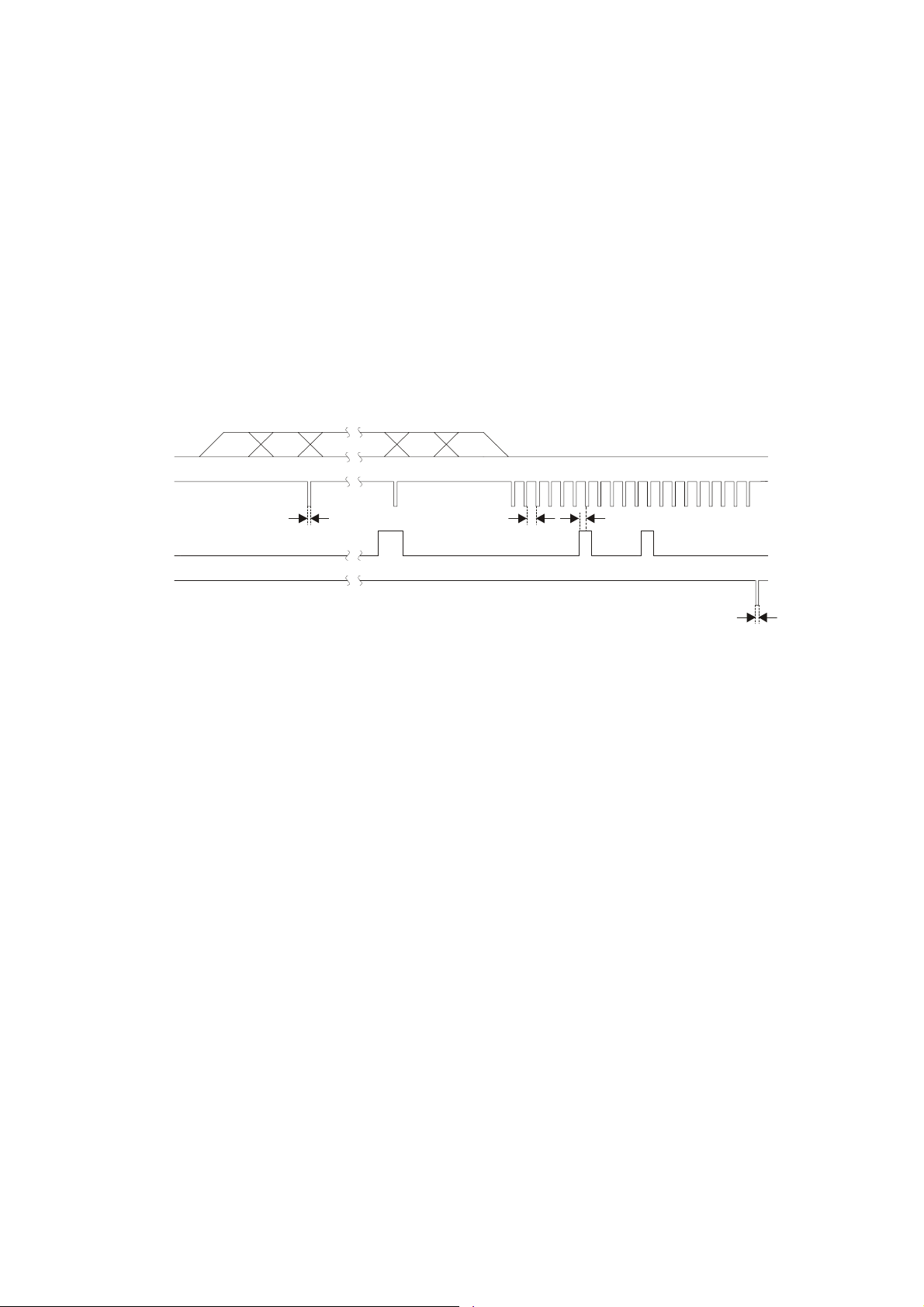
Figure 3.2, page 11 shows a full shift register cycle with keys
3, 10 and 15 activated. Key Scan represents the time when
the chip is measuring signal from each key. SCL, SDA and
LATCH represent their respective signals from the chip. SCL
is an active low clock output. SDA is the data output; high if
the key is in detect and low if it is not. LATCH pulses low
when the data transfer is complete.
Data output proceeds as soon as the key has been
processed. Most keys do not get processed during the key
scan. If so, these keys are processed and the data is output
after the complete key scan.
The internal settings of the device in Shift Register mode are
the default factory settings found in Table 6.2. This means the
device will operate with a Burst Length of 48 on all keys, and
a Sleep time of 125ms for example. These settings cannot be
changed in this mode.
In Shift Register mode, the CHANGE pin is inactive and
should be left open.
3.3 I2C Port
These devices use I2C communications, in slave mode only.
The QT60160/QT60240 will only respond to the correct
address match. I
Max Data Transfer: 100KHz
Address: 7-bit
The match address is selected via pins A0 and A1. Table 3.1
shows the address selections.
The QT60160/QT60240 allows multiple byte transmissions to
provide a more efficient communication. This is particularly
useful to retrieve several information bytes at once. Every
time the host retrieves data from the QT60160/QT60240, an
internal address pointer is incremented.
Therefore, the host only needs to write the initial address
pointer of interest (the lowest address), followed by read
cycles for as many bytes as required.
2
C operating parameters are as follows:
lQ
QT60160/60240
SDA
SCL
Latch
Figure 3.1 Shift Register Output
74HC595
Q0
27
28
9
DS
SH_CP
ST_CP
74HC595
DS
SH_CP
ST_CP
74HC595
DS
SH_CP
ST_CP
Q2
Q3
Q4
Q5
Q6
Q7
/Q7
Q0
Q2
Q3
Q4
Q5
Q6
Q7
/Q7
Q0
Q2
Q3
Q4
Q5
Q6
Q7
/Q7
Outputs, keys 16 to 23
Outputs, keys 8 to 15
Outputs, keys 0 to 7
10 QT60240-ISG R8.06/0906
3.4 CHANGE Pin
Pin 2 (CHANGE) is an active-high output that can be used to
alert the host to key touches or key releases, thus reducing
the need for wasteful I
can simply not bother to communicate with the device, except
when the CHANGE pin goes high.
CHANGE becomes active only when there is a change in key
state (either touch or touch release); CHANGE goes low
again only when the host performs a read from address 1, the
detect status register for all keys on Y0. CHANGE does not
self-clear; only an I
clear.
It is important to read all three key state addresses to ensure
the host has a complete picture of which keys have changed.
SCL
SDA
2
C communications. Normally, the host
2
C read from location 1 will cause it to
Figure 3.2 Shift Register Cycle
Key 0 Key 1 Key 2 Key 21 Key 22 Key 23Key Scan
Key 0 Key 3 Key 4 Key 23
t
SCL
In Shift Register mode the CHANGE pin does not operate
and should be left open.
Every key can be individually configured to wake a host
microcontroller upon a touch change; so, a product can wake
from sleep when any key state changes, or only when certain
desired keys change state. The configuration is set in the
Setups block (Section 6.13) on a key-by-key basis.
t
SCH
t
SDA-SCL
LATCH
t
LATCH
lQ
11 QT60240-ISG R8.06/0906

4 Control Commands
/
4.1 Introduction
The devices feature a set of commands which are used for
control and status reporting.
As well as Table 4.1 refer to Table 6.1, page 21 for further
details.
Table 4.1 Memory Map
AccessUseAddress
1
2
3
4 to 123
125
130
131 to
253
Detect status for keys 0 to 7, one bit
per key
Detect status for keys 8 to 15, one bit
per key
Detect status for keys 16 to 23, one
bit per key
Data for keys 0 to 23, in sequence.
Refer to Table 4.3 for details
Recalibrate all keys. Write 0x55 to
this address location to recalibrate all
the keys
Setups write-unlock. Write 0x55
immediately before writing setups
Poll rate: The host can make use of the CHANGE pin output
to initiate a communication; this will guarantee the optimal
polling rate.
If the host cannot make use of the CHANGE pin the poll rate
in normal ‘run’ operation should be no faster than once per
matrix scan (see Section 7.4, page 23). Typically 10 to 20ms
is more than fast enough to extract the key status. Anything
faster will not provide new information and will slow down the
chip operation.
Sending or reading the setup block is an exception, in this
case the host can send the data at the maximum possible
rate.
Run Poll Sequence: In normal run mode the host should
limit traffic with a minimalist control structure. The host should
just read the three detect status registers (see Figure 4.1,
page 14).
Repeated Start: Using repeated start is not allowed and can
cause communication failure.
4.2 Writing Data to the Device
The sequence of events required to write data to the device is
shown next.
Host to Device Device to Host
SLA+W
MemAddress
AAS
Data A P
ReadReserved0
Read
Read
Read
Read
Write
Write
Read/WriteSetups - refer to Table 5.2 for details
The host initiates the transfer by sending the START
condition, and follows this by sending the slave address of
the device together with the Write-bit. The device sends an
ACK. The host then sends the memory address within the
device it wishes to write to. The device sends an ACK. The
host transmits one or more data bytes; each will be
acknowledged by the device.
If the host sends more than one data byte, they will be written
to consecutive memory addresses. The device automatically
increments the target memory address after writing each data
byte. After writing the last data byte, the host should send the
STOP condition.
The host should not try to write beyond address 255 because
the device will not increment the internal memory address
beyond this.
4.3 Reading Data From the Device
The sequence of events required to read data from the device
is shown next.
Host to Device Device to Host
SLA+W MemAddressAASSSLA+RA
Data 1
Key
MemAddress
/A
Data 2
A
Start conditionS
Slave address plus write bitSLA+W
Acknowledge bitA
Target memory address within
device
Data from deviceData
Stop conditionP
Slave address plus read bitSLA+R
Not Acknowledge bit/indicates
last byte transmission
The host initiates the transfer by sending the START
condition, and follows this by sending the slave address of
the device together with the Write-bit. The device sends an
ACK. The host then sends the memory address within the
device it wishes to read from. The device sends an ACK.
The host must then send a STOP and a START condition
followed by the slave address again but this time
accompanied by the Read-bit. The device will return an ACK,
followed by a data byte. The host must return either an ACK
or NACK. If the host returns an ACK, the device will
subsequently transmit the data byte from the next address.
Each time a data byte is transmitted, the device automatically
increments the internal address. The device will continue to
return data bytes until the host responds with a NACK. The
host should terminate the transfer by issuing the STOP
condition.
P
A
Data n
A
P
Key
MemAddress
Start conditionS
Slave address plus write bitSLA+W
Acknowledge bitA
Target memory address within
device
Data to be writtenData
Stop conditionP
4.4 Report Detections for All Keys
Address 1: detect status for keys 0 to 7
Address 2: detect status for keys 8 to 15
Address 3: detect status for keys 16 to 23
Each location indicates all keys in detection, if any, as a
bitfield; touched keys report as 1’s, untouched or disabled
keys report as 0’s.
Note: the change pin is cleared on reading address 1.
lQ
12 QT60240-ISG R8.06/0906

Table 4.2 Bits for Key Reporting and Numbering
Address
1
2
3
Note: the device should be reset after disabling keys
because, if a key was in detect when it was disabled, it could
incorrectly report detect.
Bit Number
01234567
01234567
89101112131415
1617181920212223
4.5 Raw Data Commands
Addresses 4 to 123 allow data to be read for each key. There
are a total of 24 keys and 5 bytes of data per key, yielding a
total of 120 addresses. These addresses are read-only.
The data for the keys is mapped in sequence, starting with
key 0 at addresses 4 to 8. The data for key 15 is located at
addresses 79 to 83, and that for key 23 is located at
addresses 119 to 123. Table 4.3 summarizes this.
Table 4.3 Key Data
UseKey #Address
Signal LSB04
Signal MSB05
Reference LSB06
Reference MSB07
DetectCount (lower nibble)08
Signal LSB19
Signal MSB110
Reference LSB111
Reference MSB112
DetectCount (lower nibble)113
Signal LSB214
Signal MSB215
Reference LSB216
Reference MSB217
DetectCount (lower nibble)218
Range of values3 to 2219 to 118
Signal LSB23119
Signal MSB23120
Reference LSB23121
Reference MSB23122
DetectCount (lower nibble)23123
There are five bytes of data for each key. The first two are the
key’s 16-bit signal, and the second two are the key’s 16-bit
reference. These are followed by the Detect Integrator Count,
which is a 4-bit value stored in the lower nibble. In the case of
both the signal and reference, the 16-bit values are accessed
as two 8-bit bytes, stored LSB first.
4.6 Cal All
A value of 0x55 must be written to address 125. Upon
receiving this command the QT60xx0 will recalibrate all of the
keys. Recalibration will start at the beginning of the next full
matrix scan and last for one scan cycle.
4.7 Setups
The location “Setups write-unlock”, address 130, allows write
access to the setups. Normally the setups are write-protected;
the write-protection is engaged as soon as a read operation is
performed at any address. By writing a value of 0x55 to this
address, the write-protection is disengaged. This address is
located conveniently immediately before the setups so that
the write protection may be disengaged and the setups
written in a single I
address is undefined.
Addresses 131 to 252 provide read/write access to the
setups. Details of different setups can be found in Section 6,
page 17.
When the host is writing a new setup block the values are
being recorded into EEPROM as they arrive from the host.
2
C communication sequence. Reading this
lQ
13 QT60240-ISG R8.06/0906

Figure 4.1 Power-on or Hardware Reset Flow Chart
Power-on or
Hardware Rese t
Read key
status registers
Addr: 1, 2
and 3
Key Detection(s) / End of
Detection Processing
'CHANGE'
output set
Stuck Key
Detected
Verify Setup
Correct Setup
Block
Host main
Process
Keys OK
Block
Recalibrate All
Send 0x55 to
Setup Data
Addr 125
Incorrect
Send Correct
Setup Block
Legend
Intern a l Host
Processes
Comms
with QT
Recalibrate All
Send 0x55 to
Addr 125
lQ
14 QT60240-ISG R8.06/0906
5 I2C Operation
5.1 Interface Bus
More detailed information about I2C is available from
www.i2C-bus.org. Devices are connected onto the I
shown in Figure 5.1. Both bus lines are connected to Vdd via
pull-up resistors. The bus drivers of all I
2
C devices must be
open-drain type. This implements a wired-AND function which
allows any and all devices to drive the bus, one at a time. A
low level on the bus is generated when a device outputs a
zero.
Figure 5.1 I2C Interface Bus
Vcc
2
C bus as
5.3 START and STOP Conditions
The host initiates and terminates a data transmission. The
transmission is initiated when the host issues a START
condition on the bus, and is terminated when the host issues
a STOP condition. Between START and STOP conditions, the
bus is considered busy. As shown below, START and STOP
conditions are signaled by changing the level of the SDA line
when the SCL line is high.
Figure 5.3 START and STOP Conditions
SDA
Device 1 Device 2 Device 3 Device n R1 R2
SDA
SCL
Table 5.1 I2C Bus Specifications
UnitParameter
7-bitAddress space
100 kHzMaximum bus speed (SCL)
4µs minimumHold time START condition
4µs minimumSetup time for STOP condition
Bus free time between a STOP and START
condition
4.7µs minimum
5.2 Transferring Data Bits
Each data bit transferred on the bus is accompanied by a
pulse on the clock line. The level of the data line must be
stable when the clock line is high; The only exception to this
rule is for generating START and STOP conditions.
Figure 5.2 Data Transfer
SCL
START STOP
5.4 Address Packet Format
All address packets are 9 bits long, consisting of 7 address
bits, one READ/WRITE control bit and an acknowledge bit. If
the READ/WRITE bit is set, a read operation is performed,
otherwise a write operation is performed. When the device
recognizes that it is being addressed, it will acknowledge by
pulling SDA low in the ninth SCL (ACK) cycle. An address
packet consisting of a slave address and a READ or a
WRITE bit is called SLA+R or SLA+W, respectively.
The most significant bit of the address byte is transmitted
first. The address sent by the host must be consistent with
that selected with the option jumpers.
Figure 5.4 Address Packet Format
Addr MSB Addr LSB R/W ACK
DA
SCL
12 789
START
SDA
SCL
Data Stable Data Stable
lQ
5.5 Data Packet Format
All data packets are 9 bits long, consisting of one data byte
and an acknowledge bit. During a data transfer, the host
generates the clock and the START and STOP conditions,
while the Receiver is responsible for acknowledging the
reception. An acknowledge (ACK) is signaled by the Receiver
pulling the SDA line low during the ninth SCL cycle. If the
Receiver leaves the SDA line high, a NACK is signaled.
Data Change
15 QT60240-ISG R8.06/0906

5.6 Combining Address and Data Packets
Into a Transmission
A transmission consists of a START condition, an SLA+R/W,
one or more data packets and a STOP condition. The
wired-ANDing of the SCL line is used to implement
handshaking between the host and the device. The device
extends the SCL low period by pulling the SCL line low
whenever it needs extra time for processing between the data
transmissions.
Figure 5.5 Data Packet Format
Data MSB Data LSB ACK
Aggregate
SDA
SDA from
Transmitter
SDA from
Receiver
SCL from
Master
SLA+R/W
12 789
Figure 5.6 shows a typical data transmission. Note that
several data bytes can be transmitted between the SLA+R/W
and the STOP.
STOP,
Data Byte
or
Next Data Byte
Addr MSB Ad dr LSB R/W ACK
SDA
SCL
12 789
START SLA+R/W
Figure 5.6 Packet Transmission
Data MSB Data LSB ACK
12 789
Data Byte STOP
lQ
16 QT60240-ISG R8.06/0906
6 Setups
6.1 Introduction
The devices calibrate and process all signals using a
number of algorithms specifically designed to provide for
high survivability in the face of adverse environmental
challenges. They provide a large number of processing
options which can be user-selected to implement very
flexible, robust keypanel solutions.
User-defined Setups are employed to alter these
algorithms to suit each application. These setups are
loaded into the device over the I
Setups are stored in an onboard EEPROM array.
Many setups employ lookup-table value translation.
Table 6.2, the Setups Lookup Table on page 22 shows all
translation values. The default values are the factory
defaults.
Refer to Table 6.1 for all Setups.
6.2 Negative Threshold - NTHR
The negative threshold value is established relative to a
key’s signal reference value. The threshold is used to
determine key touch when crossed by a negative-going
signal swing after having been filtered by the detection
integrator. Larger absolute values of threshold desensitize
keys since the signal must travel farther in order to cross
the threshold level. Conversely, lower thresholds make
keys more sensitive.
As Cx and Cs drift, the reference point drift-compensates
for these changes at a user-settable rate; the threshold
level is recomputed whenever the reference point moves,
and thus it also is drift compensated.
The amount of NTHR required depends on the amount of
signal swing that occurs when a key is touched. Thicker
panels or smaller key geometries reduce ‘key gain’, i.e.
signal swing from touch, thus requiring smaller NTHR
values to detect touch.
The negative threshold is programmed on a per-key basis
using the Setup process. See
Negative hysteresis: NHYST is fixed at 12.5 percent of
the negative threshold value and cannot be altered.
Typical values: 3 to 8
(7 to 12 counts of threshold; 4 is internally added to
NTHR to generate the threshold).
Default value: 6
(10 counts of threshold)
2
C serial interfaces. The
Table 6.2, page 22.
6.3 Positive Threshold - PTHR
The positive threshold is used to provide a mechanism for
recalibration of the reference point when a key's signal
moves abruptly to the positive. This condition is not
normal, and usually occurs only after a recalibration when
an object is touching the key and is subsequently removed.
The desire is normally to recover from these events
quickly.
Positive hysteresis: PHYST is fixed at 12.5 percent of the
positive threshold value and cannot be altered.
Positive threshold levels are all fixed at six counts of signal
and cannot be modified.
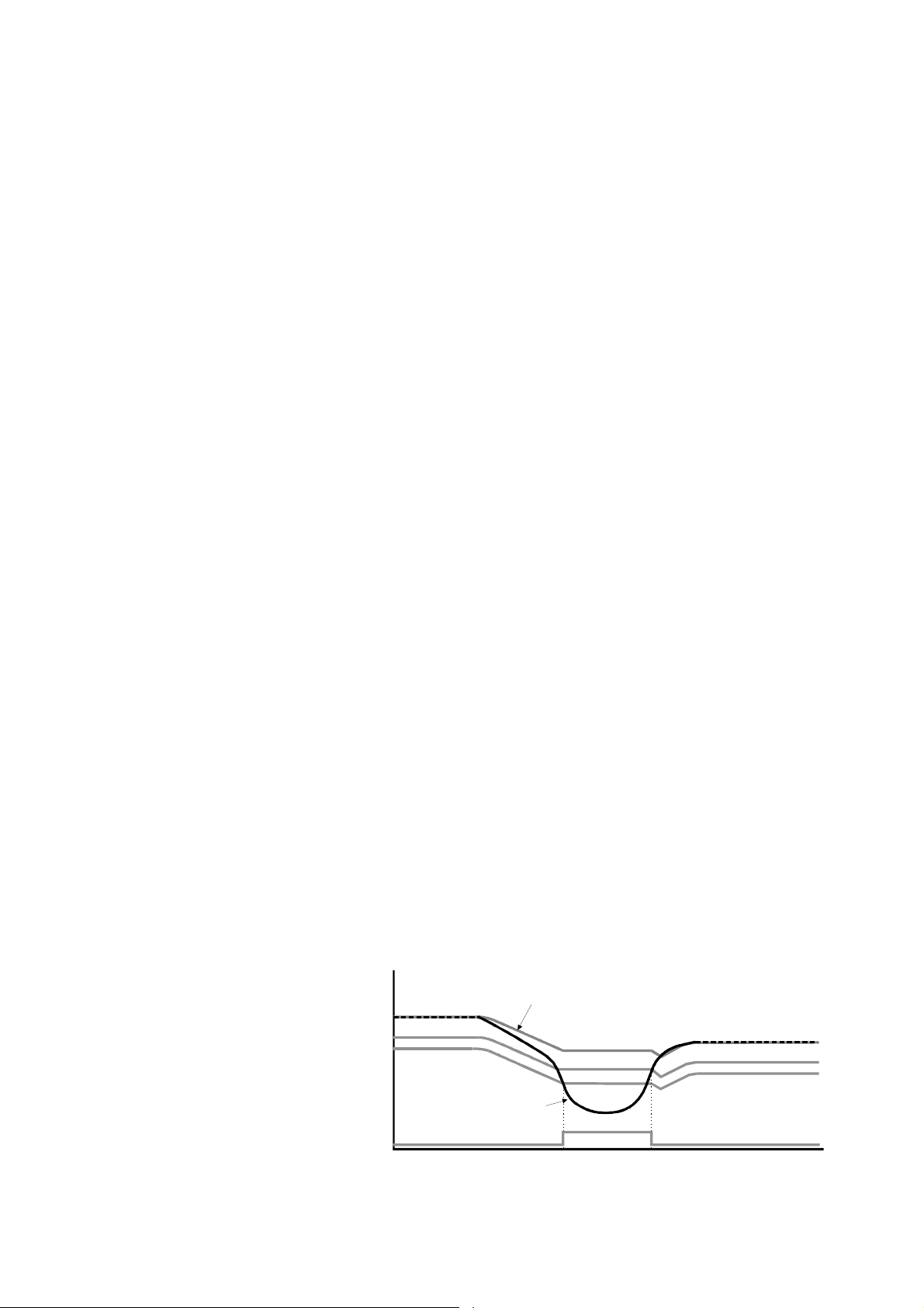
6.4 Drift Compensation - NDRIFT, PDRIFT
Signals can drift because of changes in Cx and Cs over
time and temperature. It is crucial that such drift be
compensated, else false detections and sensitivity shifts
can occur.
Drift compensation (Figure 6.1) is performed by making the
reference level track the raw signal at a slow rate, but only
while there is no detection in effect. The rate of adjustment
must be performed slowly, otherwise legitimate detections
could be ignored. The devices drift compensate using a
slew-rate limited change to the reference level; the
threshold and hysteresis values are slaved to this
reference.
When a finger is sensed, the signal falls since the human
body acts to absorb charge from the cross-coupling
between X and Y lines. An isolated, untouched foreign
object (a coin, or a water film) will cause the signal to rise
very slightly due to an enhancement of coupling. This is
contrary to the way most capacitive sensors operate.
Once a finger is sensed, the drift compensation
mechanism ceases since the signal is legitimately
detecting an object. Drift compensation only works when
the signal in question has not crossed the negative
threshold level.
The drift compensation mechanism can be asymmetric; the
drift-compensation can be made to occur in one direction
faster than it does in the other simply by changing the
NDRIFT and PDRIFT Setup parameters. This can be done
on a per-key basis.
Figure 6.1 Thresholds and Drift Compensation
lQ
Reference
Hysteresis
Threshold
Signal
Output
17 QT60240-ISG R8.06/0906

Specifically, drift compensation should be set to compensate
faster for increasing signals than for decreasing signals.
Decreasin
since an approaching finger could be compensated for
partially or entirely before even touching the touch pad.
However, an obstruction over the sense pad, for which the
sensor has already made full allowance, could suddenly be
removed leaving the sensor with an artificially suppressed
reference level and thus become insensitive to touch. In
this latter case, the sensor should compensate for the
object's removal by raising the reference level relatively
quickly.
Drift compensation and the detection time-outs work
together to provide for robust, adaptive sensing. The
time-outs provide abrupt changes in reference calibration
depending on the duration of the signal 'event'.
NDRIFT Typical values: 9 to 11
NDRIFT Default value: 10
PDRIFT Typical values: 3 to 5
PDRIFT Default value: 4
g signals should not be compensated quickly,
(2 to 3.3 seconds per count of drift compensation)
(2.5s / count of drift compensation)
(0.4 to 0.8 seconds per count of drift compensation;
translation via LUT, page )
(0.6s / count of drift compensation)
6.5 Detect Integrators - NDIL, FDIL
NDIL is used to enable or disable keys and to provide
signal filtering. To enable a key, its NDIL parameter should
be nonzero (ie NDIL=0 disables a key). See Section 2.2.
To suppress false detections caused by spurious events
like electrical noise, the devices incorporate a 'detection
integrator' or DI counter mechanism. A per-key counter is
incremented each time the key has exceeded its threshold
and stayed there for a number of acquisitions in
succession, without going below the threshold level. When
this counter reaches a preset limit the key is finally
declared to be touched.
If on any acquisition the signal is not seen to exceed the
threshold level, the counter is cleared and the process has
to start from the beginning.
The DI mechanism uses two counters. The first is the ‘fast
DI’ counter FDIL. When a key’s signal is first noted to be
below the negative threshold, the key enters ‘fast burst’
mode. In this mode the burst is rapidly repeated for up to
the specified limit count of the fast DI counter. Each key
has its own counter and its own specified fast-DI limit
(FDIL), which can range from 1 to 15. When fast-burst is
entered the QT device locks onto the key and repeats the
acquire burst until the fast-DI counter reaches FDIL, or, the
detection fails beforehand. After this the device resumes
normal keyscanning and goes on to the next key.
The ‘Normal DI’ counter counts the number of times the
fast-DI counter reached its FDIL value. The Normal DI
counter can only increment once per complete scan of all
keys. Only when the Normal DI counter reaches NDIL does
the key become formally ‘active’.
The net effect of this is that the sensor can rapidly lock
onto and confirm a detection with many confirmations,
while still scanning other keys. The ratio of ‘fast’ to ‘normal’
counts is completely user-settable via the Setups process.
The total number of required confirmations is equal to FDIL
times NDIL.
If FDIL = 5 and NDIL = 2, the total detection confirmations
required is 10, even though the device only scanned
through all keys only twice.
The DI is extremely effective at reducing false detections at
the expense of slower reaction times. In some applications
a slow reaction time is desirable. The DI can be used to
intentionally slow down touch response in order to require
the user to touch longer to operate the key.
If FDIL = 1, the device functions conventionally. Each
channel acquires only once in rotation, and the normal
detect integrator counter (NDIL) operates to confirm a
detection. Fast-DI is in essence not operational.
If FDIL m 2, then the fast-DI counter also operates in
addition to the NDIL counter.
If Signal [ NTHR: The fast-DI counter is incremented
towards FDIL due to touch.
If Signal >NTHR then the fast-DI counter is cleared due to
lack of touch.
Disabling a key: If NDIL =0, the key becomes disabled.
Keys disabled in this way are pared from the burst
sequence in order to improve sampling rates and thus
response time. See Section 2.2, page 3.
NDIL Typical values:
NDIL Default value: 2
FDIL Typical values:
FDIL Default value: 5
2, 3
4 to 6
6.6 Negative Recal Delay - NRD
If an object unintentionally contacts a key resulting in a
detection for a prolonged interval it is usually desirable to
recalibrate the key in order to restore its function, perhaps
after a time delay of some seconds.
The Negative Recal Delay timer monitors such detections;
if a detection event exceeds the timer's setting, the key will
be automatically recalibrated. After a recalibration has
taken place, the affected key will once again function
normally even if it is still being contacted by the foreign
object. This feature is set on a per-key basis using the
NRD setup parameter.
NRD can be disabled by setting it to zero (infinite timeout)
in which case the key will never auto-recalibrate during a
continuous detection (but the host could still command it).
NRD is set using one byte per key, which can range in
value from 0...254. NRD above 0 is expressed in 0.5s
increments. Thus if NRD =120, the timeout value will
actually be 60 seconds. 255 is not a legal number to use.
NRD Typical values:
NRD Default value: 20 (10 seconds)
NRD Range: 0..254 (∞, 0.5...127s)
NRD Accuracy: to within ± 250ms
20 to 60 (10 to 30 seconds)
6.7 Positive Recalibration Delay - PRD
A recalibration occurs automatically if the signal swings
more positive than the positive threshold level. This
condition can occur if there is positive drift but insufficient
positive drift compensation, or, if the reference moved
negative due to a NRD auto-recalibration, and thereafter
the signal rapidly returned to normal (positive excursion).
lQ
18 QT60240-ISG R8.06/0906

As an example of the latter, if a foreign object or a finger
contacts a key for period longer than the Negative Recal
Delay (NRD), the key is by recalibrated to a new lower
reference level. Then, when the condition causing the
negative swing ceases to exist (e.g. the object is removed)
the signal suddenly swings positive to its normal reference.
It is almost always desirable in these cases to cause the
key to recalibrate quickly so as to restore normal touch
operation. The time required to do this is governed by
PRD. In order for this to work, the signal must rise through
the positive threshold level PTHR continuously for the PRD
period.
After the PRD interval has expired and the
autorecalibration has taken place, the affected key will
once again function normally.
PRD Accuracy: to within ± 50ms
Delay: PRD is fixed at 200ms for all keys,
and cannot be altered.
6.8 Burst Length - BL
The signal gain for each key is controlled by circuit
parameters as well as the burst length.
The burst length is simply the number of times the
charge-transfer (‘QT’) process is performed on a given key.
Each QT process is simply the pulsing of an X line once,
with a corresponding Y line enabled to capture the
resulting charge passed through the key’s capacitance Cx.
QT60xx0 devices use a fixed number of QT cycles which
are executed in burst mode. There can be up to 64 QT
cycles in a burst, in accordance with the list of permitted
values shown in Table 6.2, page 22.
Increasing burst length directly affects key sensitivity. This
occurs because the accumulation of charge in the charge
integrator is directly linked to the burst length. The burst
length of each key can be set individually, allowing for
direct digital control over the signal gains of each key
individually.
Apparent touch sensitivity is also controlled by the
Negative Threshold level (NTHR). Burst length and NTHR
interact; normally burst lengths should be kept as short as
possible to limit RF emissions, but NTHR should be kept
above 6 to reduce false detections due to external noise.
The detection integrator mechanism also helps to prevent
false detections.
BL Typical values: 1, 2 (32, 48 pulses / burst)
BL Default value: 2 (48 pulses / burst)
BL Possible values: 0, 1, 2, 3 (16, 32, 48, 64
pulses/burst)
6.9 Adjacent Key Suppression - AKS
These devices incorporate adjacent key suppression
(‘AKS’ - patent pending) that can be selected on a per-key
basis. AKS permits the suppression of multiple key
presses based on relative signal strength. This feature
assists in solving the problem of surface moisture which
can bridge a key touch to an adjacent key, causing multiple
key presses. This feature is also useful for panels with
tightly spaced keys, where a fingertip might inadvertently
activate an adjacent key.
AKS works for keys that are AKS-enabled anywhere in the
matrix and is not restricted to physically adjacent keys; the
device has no knowledge of which keys are actually
physically adjacent. When enabled for a key, adjacent key
suppression causes detections on that key to be
suppressed if any other AKS-enabled key in the panel has
a more negative signal deviation from its reference.
This feature does not account for varying key gains (burst
length) but ignores the actual negative detection threshold
setting for the key. If AKS-enabled keys in a panel have
different sizes, it may be necessary to reduce the gains of
larger keys relative to smaller ones to equalize the effects
of AKS. The signal threshold of the larger keys can be
altered to compensate for this without causing problems
with key suppression.
Adjacent key suppression works to augment the natural
moisture suppression of narrow gated transfer switches
creating a more robust sensing method.
AKS Default value: 0 (Off)
6.10 Oscilloscope Sync - SSYNC
Pin 11 (S_SYNC) can output a positive pulse oscilloscope
sync that brackets the burst of a selected key. More than
one burst can output a sync pulse as determined by the
Setups parameter SSYNC for each key.
This feature is invaluable for diagnostics; without it,
observing signals clearly on an oscilloscope for a particular
burst is very difficult.
This function is supported in Quantum’s QmBtn PC
software.
SSYNC Default value: 0 (Off)
6.11 Mains Sync - MSYNC
The Mains Sync feature uses M_SYNC pin 1.
External fields can cause interference leading to false
detections or sensitivity shifts. Most fields come from AC
power sources. RFI noise sources are heavily suppressed
by the low impedance nature of the QT circuitry itself.
Noise such as from 50Hz or 60Hz fields becomes a
problem if it is uncorrelated with acquisition signal
sampling; uncorrelated noise can cause aliasing effects in
the key signals. To suppress this problem the M_SYNC
input allows bursts to synchronize to the noise source.
The noise synchronization operating mode is set by
parameter MSYNC in Setups.
The synchronization occurs only at the burst for the lowest
numbered enabled key in the matrix. The device waits for
the synchronization signal for up to 100ms after the end of
a preceding full matrix scan, then when a negative
synchronization edge is received, the matrix is scanned in
its entirety again.
The sync signal drive should be a buffered logic signal, or
perhaps a diode-clamped signal, but never a raw AC signal
from the mains. The device will synchronize to the falling
edge.
lQ
19 QT60240-ISG R8.06/0906

Since noise synchronization is highly effective and
inexpensive to implement, it is strongly advised to take
advantage of it anywhere there is a possibility of
encountering low frequency (i.e. 50/60Hz) electric fields.
Quantum’s QmBtn software can show such noise effects
on signals, and will hence assist in determining the need to
make use of this feature.
If the synchronization feature is enabled but no
synchronization signal exists, the sensor will continue to
operate but with a delay of 100ms before the start of each
matrix scan, and hence will have a slow response time.
SYNC Default value: 0 (Off)
SYNC Possible range: 0, 1 (Off, On)
6.12 Sleep Duration - SLEEP
The QT60xx0 is designed to sleep as much as possible to
conserve power. Periodically, the part wakes automatically,
scans the keyboard matrix and then returns to sleep. The
length of time the part sleeps before automatically waking
up can be configured to one of eight different values, via a
look-up table. The look-up table index must be written to
the setups (see Table 6.2, page 22).
Note that when a key changes state, the CHANGE pin can
be made to go active and the device can go into ‘fast
mode’ automatically if the WAKE feature is enabled on that
key (next section).
SLEEP default value: 3 (125ms)
SLEEP range: 0...7 (16ms...2s)
In Shift Register mode, the WAKE function is enabled for
all keys, however the CHANGE pin does not function in
this mode. The AWAKE timeout in Shift Register mode is
2.5s (note default setting of AWAKE parameter in Table
6.2).
WAKE Default value: 1 (On)
WAKE Possible range: 0, 1 (Off, On)
6.14 Awake Timeout - AWAKE
After each matrix scan, the part will automatically go to
sleep whenever possible to conserve power, unless there
has been a key state change on a key with the WAKE
feature enabled (Section 6.13), in which case the part will
wake up into ‘fast mode’ which has no sleep states and
operates at the fastest possible speed. The AWAKE
timeout feature determines how long the device will remain
in this mode from the last key state change.
Subsequent key state changes further prolong the AWAKE
interval. In other words, once the part has been awakened
by a change on a WAKE enabled key, the key response
time will be fast for as long as the keyboard remains in
use. Once key activity lapses for a period longer than the
AWAKE timeout, the part will return to sleep mode.
The AWAKE period can be configured to a value between
100ms and 25.5s, in increments of 100ms.
AWAKE default value: 25 (2.5s)
AWAKE range: 1...255 (100ms...25.5s)
AWAKE Timeout accuracy: to within ±50ms
6.13 Wake on Key Touch - WAKE
The device can be configured for full time wake-up from
Sleep mode when specific keys are touched or released
using this feature, in order to improve response time after
each key state change. Once awake the key will remain
awake until the AWAKE function times out (Section 6.14).
Also this feature makes the CHANGE pin go active on a
key touch or key release (Section 3.4).
Each key has its own WAKE configuration bit so that any
combination of keys can be configured for this function.
The time the part will remain awake after any key state
change can also be configured in the Setup block (AWAKE
feature, next section).
Any key, even one where the WAKE feature is not
enabled, will prolong the time the part remains awake once
the part is awake
6.15 Drift Hold Time - DHT
Drift Hold Time (DHT) is used to restrict drift on all keys
while one or more keys are activated. DHT defines the
length of time the drift is halted after a key detection.
This feature is particularly useful in cases of high-density
keypads where touching a key or hovering a finger over the
keypad would cause untouched keys to drift, and therefore
create a sensitivity shift, and ultimately inhibit any touch
detection.
DHT can be configured to a value of between 100ms and
25.5s, in increments of 100ms. Setting this parameter to 0
will disable this feature and the drift compensation on any
key will not be dependent on the state of other keys.
DHT default value: 10 (1s)
DHT range: 0...255 (Off, 100ms...25.5s)
lQ
20 QT60240-ISG R8.06/0906

6.16 Setups Block
Table 6.1 Setups Table
Setups data is sent from the host to the QT using the I2C interface. The setups block is memory mapped onto this interface. Thus each setup can be accessed by
reading/writing the appropriate address. Setups can be accessed individually or as a block. Before writing to any setup, an unlock code (value 0x55) must be written to the
setups write unlock address (130). Refer also to Table 6.2, page 22 for further details, and all of Section 6.
BitsValid RangeSymbolParameterBytesAddressItem
Neg thresh
1
24131...154
Neg Drift Comp
NTHR
NDRIFT
NTHR = 0...15
NDRIFT = 0...15
Key
Scope
4
4
2
Normal DI Limit
3
24179...202
Fast DI Limit
NDIL
FDIL
NDIL = 0...15
FDIL = 0...15
4
4
4
BL
WAKE = 0,1
BL = 0...3
AKS = 0,1
SSYNC = 0,1
SLEEP = 0...7
MSYNC = 0,1
Wake On Touch
Burst Length
5
6
24227...250
1251
AKS
Scope Sync
Sleep Duration
Mains Sync
WAKE
AKS
SSYNC
SLEEP
MSYNC
1
2
1
1
3
1
24
24
7
8
Default
Value
Lower nibble = Neg Threshold - take operand and add 4 to get value
1
1
1
1
1
1
1
1
6
Upper nibble = Neg Drift comp - via Lookup Table (LUT) (Table 6.2, page 22)
10
Upper nibble = Pos Drift comp - via LUT (Table 6.2, page 22)414PDRIFT = 0...15PDRIFTPos Drift Comp24155...178
Lower nibble = Normal DI Limit, values same as operand (0 = disabled burst)
2
For QT60160, only the first 16 locations are set to 2, the last eight are set to 0
5
Upper nibble = Fast DI Limit, values same as operand (0 does not work)
Range is in 0.5 sec increments; 0 = infinite, default = 10s
20180...254NRDNeg recal delay24203...226
Range is {infinite, 0.5...127s}; 255 is illegal to use
Bit 3 = WAKE, 1 - enabled
1
Bits 5, 4 = BL, via LUT (Table 6.2 page 22), default = 48
2
Bit 6 = AKS, 1 - enabled
0
Bit 7 = Scope sync, 1 = enabled
0
Bits 2,1,0 = Sleep Duration, 8 values via LUT, default = 125ms
3
Bits 6 = Mains sync, negative edge, 1 = enabled, default = off
0
Range is in 100ms increments; 1 = 100ms. Default = 2.5s. 0 is illegal to use252481...255AWAKEAwake Timeout1252
Range is in 100ms increments; 0 = disable, 1 = 100ms, default = 1s102480...255DHTDrift Hold Time1253
PageDescription
17
17
17
18
18
20
19
19
19
20
19
20
20
lQ
21 QT60240-ISG R8.06/0906

Table 6.2 Setups Lookup Table
Typical values: For most touch applications, use the values shown in the outlined cells. Bold text items indicate default settings. The number to send to the QT is the number in
the leftmost column (0...15), not numbers from within the table. The QT uses lookup tables to translate the 0.. .15 to the parameters for each function.
NRD is an exception: it can range from 0...254 which is translated from 1 = 0.5s to 254 = 127s, in increments of 0.5s, with zero = infinity. 255 is illegal.
AWAKE is an exception: it can range from 1...255 which is translated from 1 = 0.1s to 255 = 25.5s , in increments of 0.1s. Zero is illegal.
DHT is an exception: it can range from 0...255 which is translated from 1 = 0.1s to 255 = 25.5s , in increments of 0.1s. Zero will disable DHT.
Index
Number
0
1
2
3
4
5
7
8
9
11
13
NTHR
counts
17
NDRIFT
secs
0.68
PDRIFT
secs
0.30.36
- 0.6 -
NDIL
counts
- 2 -
50.80.89
FDIL
counts
2
- 5 -
881.51.512
992213
10102.5- 2.5 -1410
11113.33.315
12124.54.51612
131366
14147.57.51814
151510101915
NRD
secs
0.5 .. 127s110.20.25
Default=
10s
Parameter
WAKE
- On -
BL
Pulses
16Off0 (Infinite)unusedKey off0.10.14
- 48 -
64330.40.47
SSYNCAKS
SLEEP
ms
MSYNC
AWAKE
secs
DHT
secs
(Page 20)(Page 20)(Page 19)(Page 20)(Page 19)(Page 19)(Page 19)(Page 20)(Page 18)(Page 18)(Page 18)(Page 17)(Page 17)(Page 17)
GlobalGlobalGlobalGlobalPer keyPer keyPer keyPer keyPer keyPer keyPer keyPer keyPer keyPer key
- Off -- Off -
16
64
-125-
25044
500
1,0006611- 10 -6
2,000771.21.211
- Off -
Default=
2.5s
Offunused
0.1...25.5s0.1...25.5sOn32OnOn32
Default=
1s
lQ
22 QT60240-ISG R8.06/0906

7 Specifications
7.1 Absolute Maximum Electrical Specifications
Operating temp................................................................................... -40OC to +85OC
Storage temp.................................................................................... -55
Vdd.................................................................................................-0.5 to +5.5V
Max continuous pin current, any control or drive pin.......................................................... ±10mA
Short circuit duration to ground, any pin......................................................................infinite
Short circuit duration to Vdd, any pin........................................................................ infinite
Voltage forced onto any pin............................................................... -0.6V to (Vdd + 0.6) Volts
EEPROM setups maximum writes.............................................................. 100,000 write cycles
7.2 Recommended Operating Conditions
Vdd...............................................................................................+1.8V to 5.25V
Note: the devices will run at a minimum of 1.62V.
Supply ripple+noise........................................................................................ ±5mV
Cx transverse load capacitance per key...................................................................2 to 20pF
7.3 DC Specifications
Vdd = 5.0V, Cs = 4.7nF, Rs = 470K; Ta = recommended range, unless otherwise noted
Iddr
Idds
Average supply current,
running
Average supply current,
sleeping
1.02
2.34
4.60
3
4
6
Vdd = 1.8V
mA
µA
µA1Input leakage currentIil
bits10Acquisition resolutionAr
k✡60Internal /RST pullup resistorRrst
Vdd = 3.3V
Vdd = 5.0V
Vdd = 1.8V
Vdd = 3.3V
Vdd = 5.0V
1.8V <Vdd <5VV0.2VddLow input logic levelVil
1.8V <Vdd <5VV0.6VddHigh input logic levelVhl
V0.2Low output voltageVol
V4.2High output voltageVoh
O
C to +125OC
NotesUnitsMaxTypMinDescriptionParameter
7.4 Timing Specifications
BS
Burst spacingT
380
490
600
NotesUnitsMaxTypMinDescriptionParameter
BL = 16
µs270
BL = 32
BL = 48
BL = 64
kHz155Burst center frequencyFc
%±10Burst modulation, percentageFm
lQ
23 QT60240-ISG R8.06/0906

7.5 Power Consumption
Test condition: BL = 48, 16 or 24 keys enabled (see appropriate column)
Table 7.1 Average Current Consumption
Voltage (V)
1.8
1.8
1.8
1.8
1.8
1.8
1.8
1.8
Sleep
Setting (ms)
16
32
64
125
250
500
1000
2000
Idd Typical (mA)
16 keys24 keys
0.3600.480
0.8401.0503.3
1.5501.9005.0
0.2500.300
0.5400.6703.3
0.9101.2205.0
0.1500.170
0.3100.3503.3
0.5500.7305.0
0.0800.090
0.1700.2203.3
0.3000.4005.0
0.0480.050
0.1000.1203.3
0.1600.2405.0
0.0400.043
0.0600.0903.3
0.1100.1605.0
0.0380.040
0.0530.0803.3
0.1000.1305.0
0.0370.039
0.0500.0753.3
0.0950.1205.0
The formula to find the average current is:
Idd = (current sleeping x sleep period) + (current running x (burst spacing x number of keys enabled))
sleep period + (burst spacing x number of keys enabled)
Idd = (Idds x Tsleep) + (Iddr x (TBS x KE)) Note: there may be more than one instance of (TBS x KE)
Tsleep + (TBS x KE) (see example below)
Where:
average current (mA)=Idd
(mA)
=Idds
(Section 7.3)current when sleeping
(ms)
=Tsleep
(Table 6.2)sleep period
(Section 7.3)current when running (mA) =Iddr
1
BS
number of keys enabled
1
if more than one burst spacing is used then each must be
=KE
(ms) =T
1
(Section 7.4)burst spacing
included in the calculation.
Example: Conditions: Vdd = 1.8V, 10 keys BL = 32, 14 keys BL = 16, Tsleep = 125ms
Idd = (0.003 x 125) + (1.02 x ((0.38 x 10) + (0.27 x 14)))
= 0.06115mA = 61.15µA
125 + ((0.38 x 10) + (0.27 x 14))
lQ
24 QT60240-ISG R8.06/0906

7.6 Mechanical Dimensions
B
PIN 1
C
Dimensions in Millimeters
Symbol Minimum Nominal Maximum
A 0.80 0.90 1.00
A1 0.02 0.05
A2 0.65 1.00
A3
B
C
D 0.18 0.23 0.30
E 0.30 0.40 0.50
F 2.95 3.10 3.25
G 2.95 3.10 3.25
e 0.50 BSC
0.20 REF
5.00 BSC
5.00 BSC
F
e
G
D
A2
A
E
A3
A1
7.7 Marking
16QT60160-ISG
24QT60240-ISG
7.8 Moisture Sensitivity Level (MSL)
MarkingKeysMLF Part Number
6160
6240
SpecificationsPeak Body TemperatureMSL Rating
IPC/JEDEC J-STD-020C260OCMSL3
lQ
25 QT60240-ISG R8.06/0906

lQ
Copyright © 2006 QRG Ltd. All rights reserved
Patented and patents pending
Corporate Headquarters
1 Mitchell Point
Ensign Way, Hamble SO31 4RF
Great Britain
Tel: +44 (0)23 8056 5600 Fax: +44 (0)23 8045 3939
www.qprox.com
North America
651 Holiday Drive Bldg. 5 / 300
Pittsburgh, PA 15220 USA
Tel: 412-391-7367 Fax: 412-291-1015
This device is covered under one or more United Stat es and corresponding international patents. QRG patent num bers can be found online
at www.qprox.com. Numerous further patents are pending, which may apply to this device or the applications thereof.
The specifications set out in t his docum ent are subj ect to c hange without noti ce. All product s sold and s ervic es s upplied by QR G are subjec t
to our Terms and Conditions of sale and suppl y of services which are available online at www.qprox.com and are suppli ed with every order
acknowledgement. QRG trademark s can be found onli ne at www. qp rox. c om . Q RG product s are not s uitable f or medic al (including lif esaving
equipment), safety or mi ssion crit ical appl ications or other sim ilar purposes. Except as expressly set out in QRG's Term s and Conditions, no
licenses to patent s or other intellectual property of QRG (express or impl ied) are granted by QRG in connection with the sale of QRG
products or provision of QRG services. QRG will not be liable for customer product design and customers are entirely responsible f or their
products and applications which incorporate QRG's products.
Development Team: Samuel Brunet, Dr. Tim Ingersoll, Matthew Trend
 Loading...