

Page 1

l
lQ
Q
ll
QQ
zzzz QT401 QSlide™ enhancement - simplified calibration
zzzz Linear finger-touch capacitive slider control
z Robust Charge-Transfer sensing method
zzzz Extremely simple circuit - no external active components
zzzz SPI slave-mode interface
zzzz Self-calibration and drift compensation
z Spread-spectrum operation for optimal EMC compliance
zzzz 2.5 - 5.5V single supply operation; very low power
z Enhanced power supply & thermal drift rejection
zzzz 14-pin TSSOP Pb-free package
z Compatible with clear ITO over LCD construction
z Inexpensive, simple 1-sided PCB construction possible
APPLICATIONS
QS
LIDE
QT411-ISSG
™ T
SCLK
SNS3B
SNS3A
OUCH SLIDER
VDD 1
SDO
/SS
2
3
4
5
6
7
QT411
14
13
12
11
10
9
8
IC
GND
DRDY
DETECT
SDI
SNS1A
SNS1B
SNS2ASNS2B
y Automotive controlsy Climate controlsy Appliance controlsy Personal electronics
The QT411 QSlide™ IC is a new type of linear capacitive touch ‘slider’ sensor IC based on Quantum’s patented
charge-transfer (‘QT’) methods. This unique IC allows designers to create speed or volume controls, menu bars, and other
more exotic forms of human interface on the panel of an appliance or personal electronic device. Generally it can be used to
replace any form of linear control, through a completely sealed panel.
The device uses a simple, inexpensive resistive sensing element between four connection points. The sense element can be a
straight line or curved. The device can report a single rapid touch anywhere along the sense element, or, it can track a finger
moving along the sensing surface in real time.
This device uses three channels of synchronous sensing across a resistive element to determine touch position, using
mathematical analysis. A positional accuracy of 5% (or better) is relatively easy to achieve. The acquisitions are performed in a
burst mode which uses proprietary spread-spectrum modulation for superior noise immunity and ultra-low RF low emissions.
The output of the QT411 can also be used to create discrete controls buttons in a line, by interpreting sets of number ranges
as buttons. For example, the number range 0..19 can be button A, 30..49 button B, 60..79 button C etc. Continuous slider
action and number-range based discrete control points can be mixed on a single element, or, the element can be reinterpreted
differently at different times, for example when used adjacent to or on top of an LCD to act as a menu input device that
dynamically changes function in context. The device is compatible with ITO (Indium Tin Oxide) overlays on top of various
displays or simply to provide for a backlighting effect.
The QT411 is significantly more stable with temperature and other environmental influences than the QT401 which it is
designed to replace. In particular it can tolerate extreme temperature swings without false detection or shifts in reported touch
position. Also it does not require special calibration of the endpoints of the slider area. However, unlike the QT401 the QT411
does not have a proximity detection function.
LQ
Copyright © 2005 QRG Ltd
QT411-ISSG R6.01/1005
Page 2

1 Operation
The QT411 uses a SPI slave mode
interface for control and data
communications with a host
controller. Acquisition timings and
operating parameters are under host
control; there are no option jumpers
and the device cannot operate in a
stand-alone mode.
The output data is a 7-bit binary
number (0...127) indicating angular
position.
Like all QProx™ devices, the QT411
1= Detect Output
operates using bursts of
charge-transfer pulses; burst mode
permits an unusually high level of
control over spectral modulation,
power consumption, and response
time.
The QT411 modulates its bursts in a spread-spectrum
fashion in order to heavily suppress the effects of external
noise, and to suppress RF emissions.
1.1 Synchronized Mode
Refer also to Figure 3-1, page 6.
Sync mode allows the host device to control the rep etition
rate of the acquisition bursts, which in turn govern response
time and power consumption.
In sync mode, the device will wait for the SPI slave select line
/SS to fall and rise and will then do an acquisition burst;
actual SPI clocks and data are optional. The /SS pin thus
becomes a ‘sync’ input in addition to acting as the SPI
framing control.
Within 35µs of the last rising edge of CLK, the device will
enter a low power sleep mode. The rising edge of /SS must
occur after this time; when /SS rises, the device wakes from
sleep, and shortly thereafter does an acquisition burst. If a
more substantial sleep time is desired, /SS should be made
to rise some delay period later.
By increasing the amount of time spent in sleep mode, the
host can decrease the average current drain at the expense
of response time. Since a burst typically requires 31ms (at
3.3V, reference circuit), and an acceptable response time
might be ~100ms, the power duty cycle will be 3 1/100 or 31%
of peak current.
VIN
C1
2.2uF
SPI BUS
Regulator
VIN VOUT
GND
Figure 1-1 QT411 Wiring Diagram
1
C2
2.2uF
R2
100k
R3
1k
C3
1nF
R1
22k
13
DRDY
2
SDO
3
/SS
4
SCLK
11
SDI
12
DETECT
VDD
VSS
SNS3B
SNS3A
SNS2A
SNS2B
SNS1A
SNS1B
4
1
Rs3 4.7k
5
Cs3
100nF
6
8
Cs2
100nF
7
Rs2 4.7k
10
Cs1
100nF
9
Rs1 4.7k
Rs5 8.2k
If power is not an issue the device can run constantly under
host control, by always raising /SS after 35µs from the last
rising edge of CLK. Constant burst operation can be used by
the host to gather more data to filter the position data further
to suppress noise effects, if required.
Synchronized mode also allows the host device to control the
rate of drift compensation, by periodically sending a ‘drift’
command to the device.
Mains Sync: Sync mode can and should be used to sync to
mains frequency via the host controller, if mains interference
is possible (ie, running as a lamp dimmer control). The host
should issue SPI commands synchronously with the mains
frequency. This form of operation will heavily suppress
interference from low frequency sources (e.g. 50/60Hz),
which are not easily suppressed using spread-spectrum pulse
modulation.
Cross-talk suppression: If two or more QT411’s are used in
close proximity, or there are other QTouch™ type device(s)
close by, the devices can interfere strongly with one another
to create position jitter or false triggering. This can be
suppressed by making sure that the devices do not perform
acquisition bursts at overlapping times. The host controller
can make sure that all such devices operate in distinctly
different timeslots, by using a separate /SS line for each part.
~400k
~400k
~400k
Rs4 8.2k
'RIGHT'
'LEFT'
127
83
45
0
RESISTIVE SLIDER ELEMENT
Acquire Bur st
DRDY from QT
lQ
Figure 1-2 Free-Run Timing Diagram ( /SS = high )
~31ms ~31ms
<4ms ~30us
~25ms
2 QT411-ISSG R6.01/1005
Page 3

Table 1-1 Pin Descriptions
DESCRIPTIONTYPENAMEPIN
Positive power pin (+2.5 .. +5V)PowerVDD1
Serial data outputOSDO2
Slave Select pin. This is an active low input that enables serial communicationsI/SS3
Serial clock input. Clock idles highISCLK4
Sense pin (to Cs3, Rs3); connects to both slider ends, each via separate additional 8.2K ohm resistorsI/OSNS3B5
Sense pin (to Cs3)I/OSNS3A6
Sense pin (to Cs2, Rs2); connects to 66% point (from left) of sliderI/OSNS2B7
Sense pin (to Cs2)I/OSNS2A8
Sense pin (to Cs1, Rs1); connects to 33% point (from left) of sliderI/OSNS1B9
Sense pin (to Cs1)I/OSNS1A10
Serial data inputISDI11
ODETECT12
Active high touch detected. May be left unconnected. Note (1)
ODRDY13
Data ready output. Goes high to indicate it is possible to communicate with the QT411. Note (1)
Negative power pinGroundVSS14
Note (1): Pin floats ~400µs after wake from Sleep mode.
1.2 Free-Run Mode
If /SS stays high, the device will acquire on its own repetitively
after a timeout of about 30ms (Figure 1-2). In this mode, the
DETECT pin can be used to wake up the host when it goes
high upon touch.
In free-run mode, the device does not sleep between bursts.
In this mode the QT411 performs automatic drift
compensation at the maximum rate of one count per 1 20
acquisition burst cycles, or about one count every 7 seconds
without host intervention. It is not possible to change this
setting of drift compensation in Free-Run mode. See also
Section 3.3.3.
1.3 Sleep Mode
After an SPI transmission, the device will enter a low power
sleep state; see Figure 3-1, page 6, and Section 3.2.4, page
7 for details. This sleep state can be extended in order to
lower average power, by simply delaying the rise of /SS.
Coming out of sleep state when /SS is pulsed, the DETECT
and DRDY pins will float for ~400µs. It is recommended that
the DRDY pin be pulled to Vss with a resistor and DETECT
by bypassed with a capacitor to avoid false signalling if they
are being monitored during this time ; see Section 1.4.
Note: Pin /SS clamps to Vss for 250ns after coming out of
sleep state as a diagnostic pulse. To prevent a possible pin
drive conflict, /SS should either be driven by the host as an
open-drain pull-high drive (e.g. with a 100K pullup resistor), or
there should be a ~1K resistor placed in series with the /SS
pin. See Figure 1-1.
Note that activity on SCLK will also wake the QT411, which
in turn will then wait for the /SS to rise. For lowest possible
operation in Sleep mode, do not pulse on SCLK until after
/SS goes low.
1.4 DETECT Output Pin
This pin drives high when touch is detected and the chip is
reporting an angular position. This condition is also found as
bit 7 in the standard response.
This output will float for ~400µs during wake from Sleep mode
(see Section 1.3). It is recommended that the DETECT pin (if
it is used) be shunted to ground with a 1nF capacitor to hold
its state during the 400µs float interval when emerging from
Sleep.
Note that in the QT411, detection occurs when one or two of
the sensing channels becomes imbalanced with respect to
the other channel(s). A touch at one position will always
cause such an imbalance. However, a signal change that is
balanced among all 3 channels will not cause a detection. For
example, if a book is placed on top of the slider element, the
channels will all change in the same way and as a result,
detection will be suppressed. This feature is significantly
different from the way the QT401 operates.
1.5 Position Data
The position value is internally calculated and can be
accessed only when the sensor is touched (Detect pin high).
Direction convention: ‘Left’ is defined as the side closest to
the connection made by SNS1, and ‘Right’ is defined as the
side closest to the SNS2 connection. The ends are both
connected to SNS3, each via a resistor which allows the chip
to identify left and right as separate positions. See Figure 1-1.
The use of the terms ‘left’ and ‘right’ should not be interpreted
to mean the device can only be used in one orientation. In
fact the strip can be oriented backwards, vertically, or at any
angle.
The position on the left end reports as 0, while the position at
the right reports as 127. The device reports 45 when touched
at the SNS1 node and 83 at SNS2. The position data is a
7-bit number (0..127) that is computed in real time and is
returned via a status command.
End stops: The QT411 defines end zones of the slider
element as saturated ‘end stops’, which consist of fixed
regions where only a reading of ‘0’ or ‘127’ is returned. This is
to allow robust position detection of these important locations,
so that it is easy for a user to select ‘full off’ and ‘full on’. The
left slider end allocates 10% of the slider’s length to location
‘0’, and the right end similarly allocates 10% of the slider’s
length to location ‘127’. Only the center 80% of the slider’s
length will track changes in touch position in the range of
1..126.
The position data will update either with a single rapid touch
or will track if the finger is moved along the surface of the
lQ
3 QT411-ISSG R6.01/1005
Page 4

Figure 1-3 Conventional PCB Layout (1-sided)
Copper side faces away from the panel; the bare side is glued to the inside of the product.
element. The position data ceases to be reported when touch
detection is no longer sensed.
1.6 Calibration
Calibration is possible via two methods:
1) Power up or power cycling (there is no reset input).
2) On command from the host via the SPI port
(Command 0x01: see Section 3.3.2).
The calibration period requires 10 burst cycles, which are
executed automatically without the need for additional SPI
commands from the host. The spacing between each Cal
burst is 1ms, and the bursts average about 31ms each, i.e.
the Cal command requires ~325ms to execute. The power up
calibration has 6 extra bursts to allow for power supply
stabilization, and requires a total of ~550ms to begin normal
operation.
Calibration should be performed when there is no hand
proximity to the element, or the results may be in error.
Should this happen, the error flag (bit 1 of the standard
response, see Section 3.3) will activate when the hand is
withdrawn. In most cases this condition will self-correct if drift
compensation is used, and it can thus be ignored. See
Section 1.9 below.
Note: During calibration, the device cannot communicate.
DRDY will remain low during this interval.
electrode afterwards, so that the drift compensation
mechanism does not artificially create a threshold offset
during the iteration process. Between threshold changes, the
probe must be removed to at least 100mm from the panel.
1.8 Drift Compensation
The device features an ability to compensate for slow drift
due to environmental factors such as temperature changes or
humidity. Drift compensation is performed under host control
via a special drift command. See Section 3.3.3 for further
details.
1.9 Error Status
An error flag status is provided via a special command. An
error can only occur when a finger was touching the sensing
strip during power-on or recalibration, and then removed. In
this sequence of events, the finger is ‘calibrated away’ and is
not recognized as a touch. When the finger is removed, the
signals from the device are inverted and a position is reported
as though the strip has been touched. However, this position
report is in error.
After any calibration event (i.e. a power-on cycle or a CAL
command) the next detection event should be checked to see
if it is in error by using the special error command. If it an
error is reported, the device should be immediately calibrated
again to restore normal function (Section 3.3.2).
1.7 Sensitivity Setting
The sensitivity of the slider area to finger detection is
dependent on the values of the three Cs capacitors (Section
2.2) and the threshold setting (Section 3.3.5). Larger values
of Cs increase sensitivity and also reduce granularity (missing
codes), at the expense of higher power consumption due to
longer acquisition bursts.
The threshold setting can be used to fine tune the sensitivity
of the sensing element. When setting the threshold, use the
smallest finger size for which detection is desired (normally a
6mm diameter spot), and probe at one of the two center
connection points where sensitivity is weakest. The linear
stretches between connection points are generally slightly
higher in sensitivity due to the collection of charge from two
channels.
A ‘standard finger’ probe can be made by taking a piece of
metal foil of the required diameter, gluing it on the end of a
cylinder of sponge rubber, and connecting it to ground with a
wire. This probe is pressed against the panel centered on one
of the middle two connection points; the threshold parameter
is iterated until the sensor just detects. It is important to push
the probe into the panel quickly and not let it linger near the
lQ
2 Wiring & Parts
The device should be wired according to Figure 1-1. An
examples of a PCB layout is shown in Figure 1-3.
2.1 Electrode Construction
The strip electrode should be a resistive element of between
200K to 500K ohms (400K nominal target value) between
each set of connection points, of a suitable length and width.
Under heavy capacitive loading (for example if the element
Table 1-2 Recommended Cs vs. Materials
Thickness,
mm
0.4
0.8
1.5
2.5
3.0
4.0
4 QT411-ISSG R6.01/1005
Acrylic
(
εεεε
=2.8)
R
Borosilicate glass
εεεε
=4.8)
(
R
5.6nF10nF
10nF22nF
22nF47nF
39nF100nF
47nF-
100nF-
Page 5

must be placed immediately over a ground plane within a
millimeter), the resistance might need to be lowered. Observe
the sensing pulses for flatness on their tops in the middle of a
segment using a small coin and scope probe to make sure
the pulses fully settle before the falling edge (see app note
AN-KD02 Figure 7).
The electrode can be made of a series chain of discrete
resistors with copper pads on a PCB, or from ITO (Indium Tin
Oxide, a clear conductor used in LCD panels and touch
screens) over a display. Thick-film carbon paste can also be
used, however linearity might be a problem as these films are
notoriously difficult to control without laser trimming or
scribing.
The linearity of the sensing strip is governed largely by the
linearity and consistency of the resistive element. Position
accuracy to within 5% is routinely achievable with good grade
resistors and a uniform construction method.
2.2 Cs Sample Capacitors
Cs1, Cs2 and Cs3 are the charge sensing sample capacitors;
normally they are identical in nominal value. They should be
of type X7R dielectric.
The optimal Cs values depend on the thickness of the panel
and its dielectric constant. Lower coupling to a finger caused
by a low dielectric constant and/or thicker panel will cause the
position result to become granular and more subject to
position errors. The ideal panel is made of thin glass. The
worst panel is thick plastic. Granularity due to poor coupling
can be compensated for by the use of larger values of sample
capacitors.
A table of suggested values for no missing position values is
shown in Table 1-2. Values of Cs smaller than those shown in
the table can cause skipping of position codes. Code skipping
may be acceptable in many applications where fine position
data is not required. Smaller Cs capacitors have the
advantage of requiring shorter acquisition bursts and hence
lower power drain.
Larger values of Cs improve granularity at the expense of
longer burst lengths and hence more average power.
Cs1, Cs2 and Cs3 should be X7R type, matched to within
10% of each other (ie, 5% tolerance) for best accuracy. The
PCB reference layout (Figure 1-3) is highly recommended. If
the Cs capacitors are poorly matched, position accuracy will
be affected and there could also be missing codes.
2.3 Rs Resistors
See Figure 1-1. Rs1, Rs2, and Rs3 are low value (typically
4.7K) resistors used to suppress the effects of ESD and
assist with EMC compliance. They are optional in most
cases.
In addition, there are two 8.2K resistors required to split
channel SNS3B into the two constituent ends. These two
resistors should be placed close to the ends of the slider
strip.
2.4 Power Supply
The usual power supply considerations with QT parts applies
also to the QT411. The power should be very clean and come
from a separate regulator if possible. This is particularly
critical with the QT411 which reports continuous position as
opposed to just an on/off output.
A ceramic 0.1µF bypass capacitor should be placed very
close to the power pins of the IC.
Regulator stability: Most low power LDO regulators have
very poor transient stability, especially when the load
transitions from zero current to full operating current in a few
microseconds. With the QT411 this happens when the device
comes out of sleep mode. The regulator output can suffer
from hundreds of microseconds of instability at this time,
which will have a negative effect on acquisition accuracy.
To assist with this problem, the QT411 waits 500µs after the
400µs taken to come out of sleep mode before acquiring to
allow power to fully stabilize. This delay is not present before
an acquisition burst if there is no preceding sleep state.
Use an oscilloscope to verify that Vdd has stabilized to within
5mV or better of final settled voltage before a burst begins.
The QT411 has specially enhanced power supply rejection
built in. This means that it is often possible to share the
regulator with other circuits. However, it is always advised to
be sure that Vdd is free from spikes and transients, and is
filtered sufficiently to prevent detection problems.
During development it is wise to first design a regulator onto
the PCB just for (and next to) the QT411, but allow for it to be
‘jumpered out’. If in development it is clear that there are no
problems with false detection or ‘angle noise’ even without a
separate regulator for the QT411, then the regulator can be
safely omitted.
2.5 PCB Layout and Mounting
One form of PCB layout is shown in Figure 1-3. This is a
1-sided board; the blank side is simply adhered to the inside
of a 2mm thick (or less) control panel. Thicker panels can be
tolerated with additional position error due to capacitive ‘hand
shadow’ effects and will also have poorer EMC performance.
The Figure 1-3 layout uses a series copper pads connected
with intervening series resistors in a row. The total resistance
between any two connection points can be in the range of
100K to 500K, with ~400K being a suitable target value .
Resistance values at the higher end of this range will
generate more sensitivity provided there is no ground plane
close underneath the electrode strip.
A human finger interpolates between the copper pads (if the
pads are narrow enough) to make a smooth output with no
apparent steps. The lateral dimension along the centre of
each electrode should be no wider than the expected
smallest diameter of finger touch, to prevent stepping of the
position response (if it matters).
It is also possible create an interleaved electrode array with
only 3 resistors between each channel’s connection point on
the strip. Interleaving eliminates stepping while reducing the
number of required resistors. Consult Quantum for further
details.
Resistive inks (such as ITO, Agfa Orgacon
used if the resistance between connection points is in the
recommended range.
The electrode strip can be made in various lengths up to at
least 80mm. The electrode width should be about 12mm wide
or more, as a rule. The strip can also be an arc or other
irregular shape. For a 360 degree wheel, use the QT511 or
consult Quantum for other options.
TM
etc.) can also be
lQ
5 QT411-ISSG R6.01/1005
Page 6
The SMT components should be oriented perpendicular to
t
/
the direction of bending so that they do not fracture when the
PCB is flexed during bonding to the panel.
Additional ground area or a ground plane on the PCB will
compromise signal strength and is to be avoided. A single
sided PCB can be made of FR-2 or CEM-1 for low cost.
‘Handshadow’ effects: With thicker and wider panels an
effect known as ‘handshadow’ can become noticeable. If the
capacitive coupling from finger to electrode element is weak,
for example due to a narrow electrode width or a thick, low
dielectric constant panel, the remaining portion of the human
hand can contribute a significant portion of the total
detectable capacitive load. This will induce an offset error,
which will depend on the proximity and orientation of the hand
to the remainder of the element. Thinner panels and those
with a smaller diameter will reduce this effect since the finger
contact surface will strongly domina te the total signal, and the
remaining handshadow capacitance will not contribute
significantly to create an error offset.
PCB Cleanliness: All capacitive sensors should be treated
as highly sensitive circuits which can be influenced by stray
conductive leakage paths. QT devices have a basic
resolution in the femtofarad range; in this region, there is no
such thing as ‘no clean flux’. Flux absorbs moisture and
becomes conductive between solder joints, causing signal
drift and resultant false detections or temporary loss of
sensitivity. Conformal coatings will trap in existing amounts of
moisture which will then become highly temperature
sensitive.
The designer should specify ultrasonic cleaning as part of the
manufacturing process, and in extreme cases, the use of
conformal coatings after cleaning.
2.6 ESD, EMC and Related Issues
Please refer to Quantum app note AN-KD02 for further
information on ESD and EMC matters.
3 Serial Communications
The serial interface is a SPI slave-only mode type which is
compatible with multi-drop operation, i.e. the MISO pin will
float after a shift operation to allow other SPI devices (master
or slave) to talk over the same bus. There should be one
dedicated /SS line for each QT411 from the host controller.
A DRDY (‘data ready’) line is used to indicate to the host
controller when it is possible to talk to the QT411.
3.1 Power-up Timing Delay
Immediately after power-up, DRDY floats for approximately
20ms, then goes low. The device requires ~525ms thereafter
before DRDY goes high again, indicating that the device has
calibrated and is able to communicate.
From power up to first communication, allow a total of 550ms
in startup delay.
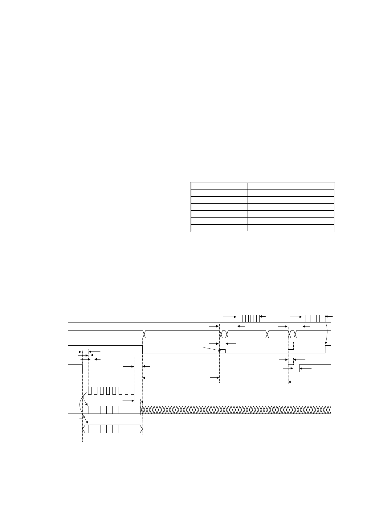
3.2 SPI Timing
The SPI interface is a five-wire slave-only type; timings are
found in Figure 3-1. The phase clocking is as follows:
HighClock idle:
Falling edge of CLK from hostData out changes on:
Rising edge of CLK from hostInput data read on:
Negative level frame from hostSlave Select /SS:
Low from QT inhibits hostData Ready DRDY:
8 bits, MSB shifts firstBit length & order:
5kHz min, 40kHz maxClock rate:
The host can shift data to and from the QT on the same cycle
(with overlapping commands). Due to the nature of SPI, the
return data from a command or request is always one SPI
cycle behind.
An acquisition burst always happens about 920µs after /SS
goes high after coming out of Sleep mode . SPI clocking
lasting more than 15ms can cause the chip to self-reset.
Figure 3-1 SPI Timing Diagram
Acquire Burs
Sleep Mode awake low-power sleep awake sleep
DRDY from QT >13us, <100us
SS from host
CLK from Host
Host Data Output
(Slave Input - MOSI)
<10us delay
QT Data Output 3-state 3-state
(Slave Out - MISO)
edge to data
>12us, <100us
>12us, <100us >20us
Data sampled on rising edge
Data shifts out on falling edge
0? 7654321
command byte
response byte
?
76543210
output driven output floats
<12us after /SS before DRDY
goes low goes low
lQ
3-state if left to float
<35us >1us, <5us
sleep until automatic wake (~3s)
data hold >=12us
after last clock
6 QT411-ISSG R6.01/1005
~31ms ~31ms
400us typ
<1ms <1ms
wake up on /SS line
Page 7

3.2.1 /SS Line
/SS acts as a framing signal for SPI data clocking under host
control. See Figure 3-1.
After a shift operation /SS must be pulsed high before being
pulsed low for 1-5 µs. This must be a minimum of 35µs after
the last clock edge on CLK. The device automatically goes
into sleep state during this interval, and wakes again after /SS
rises. If /SS is simply held low after a shift operation, the
device will remain in sleep state up to the maximum time
shown in Figure 3-1. When /SS is pulsed, another acquisition
burst is triggered.
If /SS is held high all the time, the device will burst in a
free-running mode at a ~17Hz rate. In this mode a valid
position result can be obtained quickly on demand, and/or the
DETECT pin can be used to wake the host. This rate
depends on the burst length which in turn depends on the
value of each Cs and load capacitance Cx. Smaller values of
Cs or higher values of Cx will make this rate faster.
Dummy /SS Burst Triggers: In order to force a single burst,
a dummy ‘command’ can be sent to the device by pulsing /SS
low for 10µs to 10ms; this will trigger a burst after the rising
edge of /SS without requiring an actual SPI transmission. In
order to ensure the sampling capacitors have enough time to
discharge after a short /SS pulse, DRDY is held high for
approximately 700µs before the burst occurring .
After the burst completes, DRDY will rise again to indicate
that the host can get the results.
Note: Pin /SS clamps to Vss for 250ns after coming out of
sleep state as a diagnostic pulse. To prevent a possible pin
drive conflict, /SS should either be driven by the host as an
open-drain pull-high drive (e.g. with a 100K pullup resistor), or
there should be a ~1K resistor placed in series with the /SS
pin.
3.2.2 DRDY Line
The DRDY line acts primarily as a way to inhibit the host from
clocking to the QT411 when the QT411 is busy. It also acts to
signal to the host when fresh data is available after a burst.
The host should not attempt to clock data to the QT411 when
DRDY is low, or the data will be ignored or cause a framing
error.
On power-up, DRDY will first float for about 20ms, then pull
low for ~525ms until the initial calibration cycle has
completed, then drive high to indicate completion of
calibration. The device will be ready to communicate in
typically under 600ms (with Cs1 = Cs2 = Cs3 =100nF).
While DRDY is a push-pull output ; however, this pin floats
after power-up and after wake from Sleep mode, for ~400µs
(typical at Vdd = 3.3V). It is desirable to use a pulldown
resistor on DRDY to prevent false signalling back to the host
controller; see Figure 1-1 and Section 1.3.
3.2.3 MISO / MOSI Data Lines
MISO and MOSI shift on the falling edge of each CLK pulse.
The data should be clocked in on the rising edge of CLK. This
applies to both the host and the QT411. The data path follows
a circular buffer, with data being mutually transferred from
host to QT, and QT to host, at the same time. However the
return data from the QT is always the standard response byte
regardless of the command.
The setup and hold times should be observed per Figure 3-1.
3.2.4 Sleep Mode
Please refer to Figure 3-1, page 6.
The device always enters low-power sleep mode after an SPI
transmission (Figure 3-1), at or before about 35µs after the
last rising edge of CLK. Before entering sleep mode, the
device will lower DRDY. If another immediate acquisition
burst is desired, /SS should be pulsed at least 35µs after the
last rising edge of CLK. To prolong the sleep state, it is only
necessary to pulse /SS after an even longer duration. During
this time, the QT411 will wake up approximately every 3
seconds and burst before going back to sleep. This allows
the QT411 to compensate for thermal changes.
Changes on CLK will also cause the device to wake, however
the device will not cause an acquire burst to occur if /SS has
also gone low and high again.
In sleep mode, the device consumes only a few microamps of
current. The average current can be controlled by the host, by
adjusting the percentage of time that the device spends in
sleep.
The delay between the wake signal and the following burst is
1ms max to allow power to stabilize. The DETECT and DRDY
lines will float for ~400µs (typical at Vdd = 3.3V) during wake
from Sleep mode; see Section 1.3 for details.
After each acquisition burst, DRDY will rise again to indicate
that the host can do another SPI transmission.
3.3 Commands
Commands are summarized in Table 3-1. Commands can be
overlapped, i.e. a new command can be used to shift out the
results from a prior command.
All commands cause a new acquisition burst to occur when
/SS is raised again after the command byte is fully clocked.
Standard Response: All SPI shifts return a ‘standard
response’ byte which depends on the touch detection state:
No touch detection: Bit 7 = 0 (0= not touched)
Bit 6 = 0 to indicate linear type sensor
= { 1 to indicate wheel chip }
Bits 5, 4, 3, 2: unused (report 0)
Bits 1, 0 reserved (report 0 or 1)
Is touch detection: Bit 7 = 1 (1= is touched)
Bits 0..6: Contains calculated position
Note that touch detection calculated position is based on the
results of the prior burst, which is triggered by the prior /SS
rising edge (usually, from the prior command, or, from a
dummy /SS trigger).
Bit 6 indicates the type of device: ‘1’ means that the device is
a wheel (e.g. QT501 or QT511), and ‘0’ means the device is a
linear type (e.g. QT411, or QT401).
There are 5 commands as follows.
3.3.1 0x00 - Null Command
01234567
00000000
The Null command will trigger a new acquisition (if /SS rises),
otherwise, it does nothing. The response to this command is
the Standard Response byte, returned on the next SPI shift.
lQ
7 QT411-ISSG R6.01/1005
Page 8

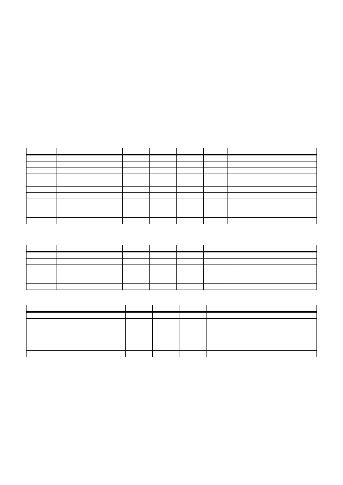
TABLE 3-1 - Command Summary
What it doesCommandHex
Shift out data; cause acquire burst (if /SS rises again)Null0x00
Calibrate0x01
Threshold0x8T
Force recalibration of reference; causes 10 sequential bursts
Power up default value = calibrated
Drift compensation request; causes acquire burst. Max drift rate is 1 count per ten 0x03 commands.Drift Comp0x03
On the following SPI shift, returns the error status of the part; causes acquire burst. See Section 3.3.4.Error Status0x04
Set touch threshold; causes acquire burst. Bottom 6 bits (‘T’) are the touch threshold value. (10TT TTTT)
Power up default value = 10
This command is predominant once the device has been
calibrated and is running normally.
3.3.2 0x01 - Calibrate
01234567
10000000
This command takes ~325ms @ 3.3V to complete.
0x01 causes the device to do a basic recalibration. After the
command is given the device will execute 10 acquisition
bursts in a row in order to perform the recalibration, without
the need for /SS to trigger each of the bursts. The host should
wait for DRDY to rise again after the calibration has
completed before shifting commands again.
This command should be given if there is an error
reported via the 0x04 command.
On power-up the device calibrates itself automatically and so
a 0x01 command is not required on startup.
The response to this command is the Standard Response
byte, returned on the next SPI shift. During calibration,
device communications are suspended.
3.3.3 0x03 - Drift Compensate
01234567
11000000
0x03 causes the sensor to perform incremental drift
compensation. This command must be given periodically in
order to allow the sensor to compensate for drift. The more
0x03 commands issued as a percentage of all commands,
the faster the drift compensation will be.
The 0x03 command must be given 10 times in order for the
device to do one count of drift compensation in either
direction. The 0x03 command should be used in substitution
of the Null command periodically.
Example: The host causes a burst to occur by sending a
0x00 Null command every 50ms (20 per second). Every 10th
command the host sends is a 0x03 (drift) command.
The maximum drift compensation slew rate in the reference
level is -
50ms x 10 x 10 = 5.0 seconds
The actual rate of change of the reference level depends on
whether there is an offset in the signal with respect to the
reference level, and whether this offset is continuous or not.
It is possible to modulate the drift compensation rate
dynamically depending on circumstances, for example a
significant rate of change in temperature, by varying the mix
of Drift and Null commands.
If the Drift command is issued while the device is in touch
detection (ie bit 7 of the Standard Response byte =1), the drift
function is ignored.
Drift compensation during Free-Run mode is fixed at 6, which
results in a maximum rate of drift compensation rate of about
3secs / count; see Section 1.2.
The drift compensation rate should be made slow, so that it
does not interfere with finger detection. A drift compensation
rate of 3s ~ 5s is suitable for almost all applications. If the
setting is too fast, the device can become u nnecessarily
desensitized when a hand lingers near the element. Most
environmental drift rates are of the order of 10's or 100's of
seconds per count.
The response to this command is the Standard Response
byte, returned on the next SPI shift.
3.3.4 0x04 - Error Status
01234567
00100000
This command is used to read the current status of the
device. In particular it is used to detect if there is a sensing
error caused by a calibration or power-on at a bad time, ie
when a finger is on the sensing strip and thereafter removed.
The reported bits are as follows:
Bit 7 = 1 indicates touch;
= 0 indicates no touch
Bit 6 = 0 indicates Linear type (QT401 or QT411)
= 1 indicates Wheel type (QT510 or QT511)
Bits 5, 4, 3, 2: unused (0)
Bit 1 = 1 if calibration error
Bit 0 reserved (reports 0 or 1)
All bits except Bit 1 can be safely ignored.
The status byte should be read the first time there is a
detection just after a power-on reset or after a 0x01
calibration. If Bit 1 = 1, there was a calibration error and the
device should be immediately calibrated again using the 0x01
command. After the second calibration it should be checked
yet again (and so on) until there is no error.
If there is no error according to the sequence of the above
paragraph, it is not required to read this byte again.
The error byte is returned on the following SPI shift.
lQ
8 QT411-ISSG R6.01/1005
Page 9

3.3.5 0x8T - Set Touch Threshold
01234567
T
T
T
T
T
T
01
4
5
2
3
The lower 6 bits of this command (T5..T0) are used to set the
touch threshold level. Higher numbers are less sensitive (ie
the signal has to travel further to cross the threshold).
Operand ‘T’ can range from 0 to 63. Internally the number is
multiplied by 4 to achieve a wider range. 0 should never be
used.
This number is normally set to 10, more or less depending on
the desired sensitivity to touch and the panel thickness.
Touch detection uses a hysteresis value equal to 12.5% of
the threshold setting.
Both the touch bit (bit 7) in the standard response and the
DETECT pin will go high if this threshold is crossed. The
DETECT pin can be used to indicate to the host that the
device has detected a finger, without the need for SPI polling.
However the /SS line must remain high constantly so that the
device continues to acquire continuously, or /SS has to be at
least pulsed regularly for this to work.
0
1
The response to this command is the Standard Response
byte, returned on the next SPI shift.
0x8T power-up default setting: 10
3.4 SPI - What to Send
The host should execute the following commands after
powerup self-cal cycle has completed (assuming a 50ms SPI
repetition rate):
1. 0x01 - Basic calibration (optional as this is done
automatically on power-up)
2. 0x8T - Set touch threshold (optional)
3. An endlessly repeating mixture of:
a. 0x00 (Null) - all commands except:
b. 0x03 (Drift compensate) - replace every nth Null
command with 0x03 where typically, n = 10
c. 0x04 (Error status) - use after any detection just
after a calibration or power-up to see if there is a
calibration error.
Note: the Null can be replaced by an empty /SS pulse if there
is no need for fast updates.
lQ
9 QT411-ISSG R6.01/1005
Page 10
4.1 Absolute Maximum Specifications
Operating temperature range, Ta....................................................................... -40OC to +85OC
Storage temperature range, Ts........................................................................ -55
V
DD
.....................................................................................................-0.5 to +7.0V
Max continuous pin current, any control or drive pin .............................................................. ±20mA
Short circuit duration to ground, any pin ..........................................................................infinite
Short circuit duration to V
DD
, any pin.............................................................................infinite
Voltage forced onto any pin................................................................... -0.6V to (Vdd + 0.6) Volts
O
C to +125OC
4.2 Recommended Operating Conditions
VDD..................................................................................................... +2.5 to 5.0V
Supply ripple+noise......................................................................................5mV p-p max
Cs1, Cs2, Cs3................................................................................................. 100nF
Cs1, Cs2, Cs3 relative matching.................................................................................. ±5%
Output load, max............................................................................................. ±0.5mA
4.3 DC Specifications
Vdd = 5.0V, Cs1 = Cs2 = 100nF, 100ms rep rate, Ta = recommended range, all unless otherwise noted
NotesUnitsMaxTypMinDescriptionParameter
@ 5VmA1.50.75Peak supply currentIDD5
@ 3VmA0.60.45Peak supply currentIDD3
@ 5VµA180Average supply currentIDD5
@ 3VµA110Average supply currentIDD3
Required for proper startup and calibrationV/s100Supply turn-on slopeV
V0.8Low input logic levelV
V2.2High input logic levelV
4mA sinkV0.6Low output voltageV
1mA sourceVVdd-0.7High output voltageV
µA±1Input leakage currentI
DDS
HL
OL
OH
IL
P
P
A
A
IL
R
bits7Acquisition resolutionA
4.4 AC Specifications
Vdd = 5.0V, Cs1 = Cs2 = 100nF, Ta = recommended range, unless otherwise noted
R
T
QT
BS
D
SPI
4.5 Signal Processing and Output
P
T
P
T
R
L
NotesUnitsMaxTypMinDescriptionParameter
Under host controlms-Response timeT
Variable parameter under host controlpF 0.6Touch SensitivityS
Modulated spread-spectrum (chirp)kHz1049892Sample frequencyF
ms1QT Burst spacingT
ms550Power-up delay to operateT
kHz37 5SPI clock rateF
NotesUnitsMaxTypMinDescriptionParameter
Both prox and touch detectioncounts1Detection integrator countsDI
Host controlled variable631Threshold, proxT
Host controlled variable631Threshold, wheel touchT
% of threshold setting%0Hysteresis, prox sensingH
% of threshold setting%12.5Hysteresis, touch sensingH
% of bursts; host controlled%±10Drift compensation rateD
Depends on element linearity, layout%±3Position linearity
lQ
10 QT411-ISSG R6.01/1005
Page 11

4.6 TSSOP Package
B
E
E1
D
2
n
1
A
a
c
Dimension Limits
Number of Pins n 14 14
Pitc h p 0.026 0.65
Overall Height A 0.043 1.10
Standoff A1 0.002 0.004 0.006 0.05 0.10 0.15
Overall W idth E 0.246 0.251 0.256 6.25 6.38 6.50
Moulded P ack age W idth E1 0.169 0.173 0.177 4.30 4.40 4.50
Moulded P ack age Length D 0.193 0.197 0.201 4.90 5.00 5.10
Foot Length L 0.020 0.024 0.028 0.50 0.60 0.70
FootAngle 048048
Lead Thicknes s c 0.004 0.006 0.008 0.09 0.15 0.20
Lead W idth B 0.007 0.010 0.012 0.19 0.25 0.30
MouldDraftAngleTop a 05100510
MouldDraftAngleBottom 0 5 10 0 5 10
4.7 Ordering Information
Units
L
A1
MILLIMETERSINCHES
MIN NOM MAX MIN NOM MAX
MARKINGTEMP RANGEPACKAGEPART NO.
QT411-400C ~ +850CTSSOP-14QT411-ISSG
lQ
11 QT411-ISSG R6.01/1005
Page 12

lQ
Copyright © 2004-2005 QRG Ltd. All rights reserved.
Patented and patents pending
Corporate Headquarters
1 Mitchell Point
Ensign Way, Hamble SO31 4RF
Great Britain
Tel: +44 (0)23 8056 5600 Fax: +44 (0)23 80565600
www.qprox.com
North America
651 Holiday Drive Bldg. 5 / 300
Pittsburgh, PA 15220 USA
Tel: 412-391-7367 Fax: 412-291-1015
This device covered under one or more of the following United States and corresponding international patents: 5,730,165, 6,288,707,
6,377,009, 6,452,514, 6,457,355, 6,466,036, 6,535,200. Numerous further patents are pending which may apply to this device or the
applications thereof.
The specifications set out in this document are subject to change without notice. All products sold and services supplied by QRG are subject
to our Terms and Conditions of sale and supply of services which are available online at www.qprox.com and are supplied with every order
acknowledgment. QProx, QTouch, QMatrix, QLevel, QWheel, QView, QScreen, and QSlide are trademarks of QRG. QRG products are not
suitable for medical (including lifesaving equipment), safety or mission critical applications or other similar purposes. Except as expressly set
out in QRG's Terms and Conditions, no licenses to patents or other intellectual property of QRG (express or implied) are granted by QRG in
connection with the sale of QRG products or provision of QRG services. QRG will not be liable for customer product design and customers
are entirely responsible for their products and applications which incorporate QRG's products.
Development Team: Martin Simmons, Matthew Trend
 Loading...