

Page 1
lQ QT240
z Four independent charge-transfer (‘QT’) touch keys
z Individual outputs per channel - active high
z Projects prox fields through any dielectric
z Sensitivity easily adjusted on a per-channel basis
z 100% autocal for life - no adjustments required
z 3.9V ~ 5.5V single supply operation
z 10s, 60s, infinite auto-recal timeout (strap options)
z Sync pin for line sync to suppress noise
z Spread spectrum operation
z Pin options for auto recalibration timings
z Extremely low cost per key
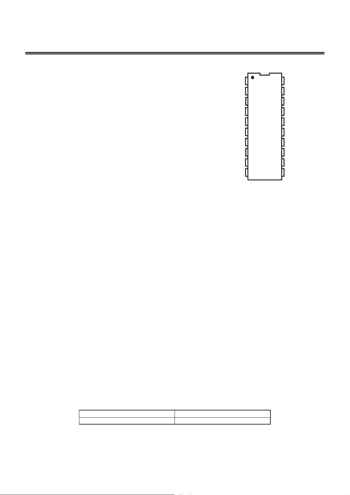
z 20-SSOP Pb-free package
APPLICATIONS
PC Peripherals
Backlighted buttons
Appliance controls
Security systems
4 KEY QT
SNS2
SNS1
SNS1K
OUT1
OUT2
OUT3
VSS
SS/SYNC
n.c. n.c.
Access systems
Pointing devices
OUCH
1
2
3
4
5
6
7
8
9
10
™ S
QT240
20-SSOP
ENSOR
SNS3K
20
SNS3SNS2K
19
SNS4K
18
SNS4
17
n.c.
16
OSC
15
VDD
14
/RES
13
OUT4
12
11
IC
Instrument panels
Gaming machines
The QT240 charge-transfer (“QT’”) QTouch IC is a self-contained digital sensor IC capable of detecting near-proximity or touch
on 4 electrodes. It allows electrodes to project independent sense fields through any dielectric like glass, plastic, stone,
ceramic, and wood. It can also turn metal-bearing objects into intrinsic sensors, making them responsive to proximity or touch.
This capability coupled with its continuous self-calibration feature can lead to entirely new product concepts , adding high value
to product designs.
Each of the channels operates independently of the other s, and each can be tuned for a unique sensitivity level by simply
changing its sample capacitor value. Two speeds are supported, one of which consumes on ly 90µA of typical current at 4V.
Unique among capacitance sensors, the device incorporates spread spectrum modulation for unsurpassed EMC compliance.
The devices are designed specifically for human interfaces, like control panels, appliances, gaming devices, lighting controls,
or anywhere a mechanical switch or button may be found; they may also be used for some material sensing and control
applications.
These devices feature a SYNC pin which allows for synchronization with additional similar parts and/or to an external source to
suppress interference. This pin doubles as a drive pin for spread-spectrum modulation. Option pins are provided which allow
different timing and feature settings.
The RISC core of these devices use signal processing techniques pioneered by Quantum which are designed to survive
numerous real-world challenges, such as ‘stuck sensor’ conditions, component ageing, moisture films, and signal drift.
By using the charge transfer principle, these devices deliver a level of performance clearly superior to older technologies yet
are highly cost-effective.
AVAILABLE OPTIONS
A
SSOP-20T
QT240-ISS-G-400C to +850C
LQ
Copyright © 2003 QRG Ltd
QT240R R1.10/0905
Page 2
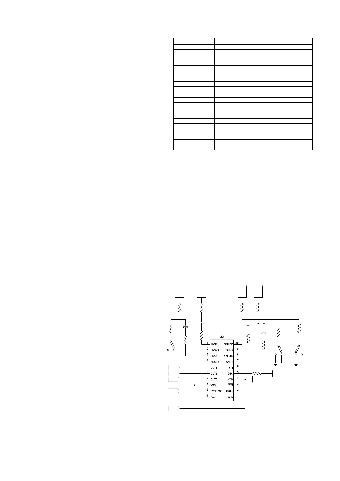
1 - OVERVIEW
QT240 devices are burst mode digital charge-transfer (QT)
sensor ICs designed specifically for touch controls; they
include all hardware and signal processing functions
necessary to provide stable sensing under a wide variety of
conditions. Only a single low cost capacitor per channel is
required for operation.
Figures 1-1 and 1-2 show basic circuits for these device s.
See Table 1-1 for device pin listings.
The devices employ bursts of charge-transfer cycles to
acquire signals. Burst mode permits low power operation,
dramatically reduces RF emissions, lowers susceptibility to
RF fields, and yet permits excellent speed. Internally, signals
are digitally processed to reject impulse noise using a
'consensus' filter that requires six consecutive confirmations
of detection.
The QT switches and charge measurement hardware
functions are all internal to the device. A single-slope
switched capacitor ADC includes the QT charge and transfer
switches in a configuration that provides direct ADC
conversion; an external Cs capacitor accumulates the charge
from sense-plate Cx, which is then measured.
Larger values of Cx cause the charge transferred into Cs to
rise more rapidly, reducing available resolution; as a
minimum resolution is required for proper operation, this can
result in dramatically reduced gain. Larger values of Cs
reduce the rise of differential voltage across it, increasing
available resolution by permitting longer QT bursts. The
value of Cs can thus be increased to allow larger values of
Cx to be tolerated. The IC is responsive to both Cx and Cs,
and changes in either can result in substantial changes in
sensor gain.
Unused channels: If a channel is not used, a dummy sense
capacitor (nominal value: 1nF) of any type plus a 2.2K series
resistor must be connected between unused SNS pin pairs
ensure correct operation.
T
ABLE
1-1 PIN L
ISTING
- QT240-ISS
DescriptionNamePin
Sense pin (to Rs2 + Cs2)SNS21
Sense pin (to Cs2, electrode)SNS2K2
Sense pin (to Rs1 + Cs1)SNS13
Sense pin (to Cs1, electrode); speed optionSNS1K4
Output, key 1OUT15
Output, key 2OUT26
Output, key 3OUT37
GroundVSS8
Sync in and/or spread spectrum driveSYNC/SS9
Unbonded internallyn.c.10
Unbonded internallyn.c.11
Output, key 4OUT412
Reset pin, active low. Can usually tie to Vdd./RES13
Power: +4.0 to +5V locally regulatedVDD14
Oscillator bias inOSC15
Ground or no connectVSS16
Sense pin (to Rs4 + Cs4)SNS417
Sense pin (to Cs4, electrode); OPT2SNS4K18
Sense pin (to Rs3 + Cs3)SNS319
Sense pin (to Cs3, electrode); OPT1SNS3K20
optional passive parts (if desired ). Sync operation is not
supported in this mode.
1.2 ELECTRODE DRIVE; WIRING
The QT240 has four completely independent sensing
channels. The conversion process treats Cs on each channel
as a floating transfer capacitor; as a direct result, sense
electrodes can be connected to either SNS pin and the
sensitivity and basic function will be the same; however
electrodes should be connected to SNSnK lines to reduce
EMI susceptibility.
The PCB traces, wiring, and any components associated
with or in contact with either SNS pin will become touch
sensitive and should be treated with caution to limit the touch
area to the desired location.
1.1 OPERATING MODES
The QT240 features spread-spectrum acquisition
capability, external synchronization of acquire
bursts, and fast and slow acquisition modes. These
modes are enabled via high-value resistors
connected to the SNS pins to ground or Vdd. These
resistors are required in every circuit.
There are two basic modes as shown in Figures 1-1
and 1-2.
Low-power Sync mode: In this mode the device
operates with about a 100ms response time and
very low current (about 90µA average at 4.0V). This
mode allows the device to be synchronized to an
external clock source, which can be used to either
suppress external interference (such as from
50/60Hz wiring) or to decrease response time
(which will also increase power consumption).
Spread-spectrum operation is not directly supported
in this mode. Sync usage is optional; the Sync pin
should simply be grounded if unused.
Fast, Spread-Spectrum mode: In this mode the
device operates with ~40ms response times but
higher current drain (~1.5mA @ 4.0V). This mode
also supports spread-spectrum operation via a few
lQ
F
IGURE
S1
SPEED
OPT
R1
1M
VDD
OUT1
OUT2
OUT3
SYNC
OUT4
1-1 LOW P
KEY 1
RSNS1
22K
CS1
10nF
RS1
2.2K
KEY 2
CS2
10nF
RSNS2
22K
RS2
2.2K
OWER
QT240-ISS
, S
YNCHRONIZED CIRCUIT
KEY 3
KEY 4
RSNS4
RSNS3
22K
22K
CS3
10nF
CS4
10nF
RS3
2.2K
RS4
2.2K
62K
R4
VDD
10 second
timeout shown
R3
1M
S3
OPT2
VDD
VDD
2 QT240R R1.10/0905
OPT1
R2
1M
S2
VDD
Page 3
F
IGURE
1-2 F
AST
, S
PREAD-SPECTRUM CIRCUIT
RSNS4
CS4
10nF
RS4
2.2K
R5
360K
C1
22nF
10 second
timeout shown
R3
1M
S3
OPT2
VDD
62K R4
R6
180K
SPEED
OPT
KEY 3
RSNS3
22K
CS3
10nF
RS3
2.2K
KEY 4
22K
VDD
CS1
10nF
RS1
2.2K
KEY 2
RSNS2
22K
CS2
10nF
RS2
2.2K
QT240_ISS
KEY 1
RSNS1
22K
R1
1M
S1
VDD
OUT1
OUT2
OUT3
OUT4
Multiple touch electrodes connected to any SNSnK can be
used, for example to create control surfaces on both sides of
an object.
It is important to limit the amount of stray capacitance on the
SNS terminals, for example by minimizing trace lengths and
widths to allow for higher gain without requiring higher values
of Cs. Under heavy delta-Cx loading of one key, cross
coupling to another key’s trace can cause the other key to
trigger. Therefore, electrode traces from adjacent keys
should not be run close to each other over long runs in order
to minimize cross-coupling if large values of delta-Cx are
expected, for example when an electrode is directly touched.
This is not a problem when the electrodes are working
through a plastic panel with normal touch sensitivity.
1.3 SENSITIVITY
Sensitivity can be altered to suit various applications and
situations on a channel-by-channel basis. The easiest and
most direct way to impact sensitivity is to alter the value of
each Cs; more Cs yields higher sensitivity. Each channel has
its own Cs value and can therefore be independently
adjusted.
Figure 2-1 Drift Compensation
Signal
Threshold
Reference
Output
Hysteresis
1.3.1 A
LTERNATIVE WAYS TO INCREASE SENSITIVITY
Sensitivity can also be increased by using bigger
electrode areas, reducing panel thickness, or using
a panel material with a higher dielectric constant .
1.3.2 D
ECREASING SENSITIVITY
In some cases the circuit may be too sensitive.
Gain can be lowered further by a number of
R2
1M
OPT1
VDD
strategies: a) making the electrode smaller, b)
making the electrode into a sparse mesh using a
high space-to-conductor ratio, or c) by decreasing
S2
the Cs capacitors.
1.3.3 KEY B
ALANCE
A number of factors can cause sensitivity
imbalances. Notably, SNS wiring to electrodes can
VDD
have differing stray amounts of capacitance to
ground. Increasing load capacitance will cause a
decrease in gain. Key size differences, and
proximity to other metal surfaces can also impact
gain.
The four keys may thus require ‘balancing’ to
achieve similar sensitivity levels. This can be best
accomplished by trimming the values of the four
Cs capacitors to achieve equilibrium. The four Rs
resistors have no effect on sensitivity and should
not be altered. Load capacitances can also be
added to overly sensitive channels to ground, to reduce their
gains. These should be on the order of a few picofarads.
2 - QT240 SPECIFICS
2.1 SIGNAL PROCESSING
These devices process all signals using 16 bit math , using a
number of algorithms pioneered by Quantum. These
algorithms are specifically designed to provide for high
survivability in the face of adverse environmental changes.
2.1.1 D
Signal drift can occur because of changes in Cx , Cs, and
Vdd over time. If a low grade Cs capacitor is chosen, the
signal can drift greatly with temperature. If keys are subject
to extremes of temperature or humidity, the signal can also
drift. It is crucial that drift be compensated, else false
detections, non-detections, and sensitivity shifts will follow.
Drift compensation (Figure 2-1) is a method that makes the
reference level track the raw signal at a slow rate, only while
no detection is in effect. The rate of reference adjustment
RIFT COMPENSATION
must be performed slowly else legitimate detections
can also be ignored. The IC drift compensates each
channel independently using a slew-rate limited
change to the reference level; the threshold and
hysteresis values are slaved to this reference .
Once an object is sensed, the drift compensation
mechanism ceases since the signal is legitimately
high, and therefore should not cause the reference
level to change.
The signal drift compensation is 'asymmetric'; the
reference level drift-compensates in one direction
faster than it does in the other. Specifically, it
compensates faster for decreasing signals than for
increasing signals. Increasing signals should not be
lQ
3 QT240R R1.10/0905
Page 4

compensated for quickly, since an approaching finger could
be compensated for partially or entirely before even
approaching the sense electrode. However, an obstruction
over the sense pad, for which the sensor has already made
full allowance for, could suddenly be removed leaving the
sensor with an artificially elevated reference level and thus
become insensitive to touch. In this latter case, the sensor
will compensate for the object's removal very quickly, usually
in only a few seconds.
With large values of Cs and small values of Cx, drift
compensation will appear to operate more slowly than with
the converse.
Drift Compensation in Slow Mode: Drift compensation
rates in Slow mode are preserved if there is no Sync signal,
and the rates are derived from the ~90ms Sleep interval.
However if there is a Sync signal, then drift compensation
rates are derived from an assumption that the Sync
periodicity is ~18ms (which is corresponds to 55.5Hz). Thus,
drift compensation timings in Sync mode are correct for an
~18ms Sync period but different (slower or faster) for other
Sync periods. For example a Sync period of 36ms would
halve the expected drift compensation rates.
2.1.2 T
The internal threshold level is fixed at 12 counts for all four
channels. The hysteresis is fixed at 2 counts (17%).
2.1.3 MAX ON-D
If a sufficiently large object contacts a key for a prolonged
duration, the signal will trigger a detection output preventing
further normal operation. To cure such ‘stuck key’ conditions ,
the sensor includes a timer on each channel to monitor
detection duration. If a detection exceeds the maximum timer
setting, the timer causes the sensor to perform a full
recalibration (if not set for infinite) . This is known as the Max
On-Duration feature.
After the Max On-Duration interval, the sensor channel will
once again function normally, even if partially or fully
obstructed, to the best of its ability given electrode
conditions. There are three timeout durations available via
strap option: 10s, 60s, and infinite (Table 2-2).
Max On-Duration works independently per channel; a
timeout on one channel has no effect on another channel.
Note also that the timings in Table 2-2 are dependent on the
oscillator frequency in fast mode. Doubling the
recommended frequency will halve the timeouts. This is not
true in Slow mode.
Infinite timeout is useful in applications where a prolonged
detection can occur and where the output must reflect the
detection no matter how long. In infinite timeout mode, the
designer should take care to be sure that drift in Cs, Cx, and
Vdd do not cause the device to ‘stick on’ inadvertently even
when the target object is removed from the sense field.
Timeouts are approximate and can vary substantially over
Vdd and temperature, and should not be relied upon for
critical functions. Timeouts are also dependent on operating
frequency in Fast mode.
Max On-Duration in Slow Mode: When Sync mode is used
in Slow mode, the Max On-Duration timings are derived from
the Sync period. The device assumes the Sync periodicity is
18ms (midway between 50Hz and 60Hz sync timings). Thus,
Max On-Duration timings in Sync mode are correct for an
HRESHOLD LEVEL
URATION
18ms Sync period but different (shorter or longer) for other
Sync periods. For example a Sync period of 36ms would
double all expected Max On-Duration timings.
2.1.4 D
It is desirable to suppress false detections due to electrical
noise or from quick brushes with an object. To this end,
these devices incorporate a per-key ‘Detection Integrator’
counter that increments with each signal detection exceeding
the signal threshold (Figure 2-1) until a limit count is
reached, after which an Out pin becomes active. If a ‘no
detect’ is sensed even once prior to the limit, this counter is
reset to zero and no detect output is generated. The required
limit count is 6.
The Detection Integrator can also be viewed as a
'consensus' vote requiring a detection in successive samples
to trigger an active output.
In slow mode, the detect integrator forces the device to
operate faster to confirm a detection. The six successive
acquisitions required to affirm a detection are done without
benefit of a low power sleep mode between bursts.
2.1.5 F
Pin 13 is a Reset pin, active-low, which in cases where
power is clean can be simply tied to Vdd. On power-up, the
device will automatically recalibrate all channels of sensing.
Pin 13 can also be controlled by logic or a microcontroller to
force the chip to recalibrate, by toggling it low for 10µs or
more, then raising it high again.
2.1.6 F
If the sensed capacitance becomes lower by 5 counts than
the reference level for 2 seconds, the sensor will consider
this to be an error condition and will force a recalibration on
the affected channel.
ETECTION INTEGRATOR
ORCED SENSOR RECALIBRATION
AST POSITIVE RECALIBRATION
2.2 OPTIONS
These devices are designed for maximum flexibility and can
accommodate most popular sensing requirements via option
pins.
The option pins are read on power-up and about once every
10 seconds while the device is not detecting touch on any
channel. Options are set using high value resistors
connected to certain SNS pins, to either Vdd or Vss. These
options are read 25 times over 250µs to ensure that they are
not influenced by noise pulses. All 25 samples must agree.
However, large values of Cx on the SNS wires can load
down the pins to the point where the 1M pullup resistors
cannot pull high fast enough, and the pins are read
erroneously as a result. Cx should be below 50pF to prevent
errors; this value can be read with a conventional
capacitance meter with the QT240 removed.
The option setting resistors are mandatory and cannot be
deleted. The must be strapped to either Vdd or Vss.
Speed option (Strap S1): This jumper selects whether the
device acts in a slower, low power mode with a response
time of approximately 100ms, or in a fast mode with a
response time of 40ms typical. Fast mode consumes
substantially more power than the slow mode, but also
enables the use of spread-spectrum detection. Only slow
mode supports the use of external Sync (Section 2.3).
lQ
4 QT240R R1.10/0905
Page 5

T
ABLE
2-1 S1 S
T
ABLE
2-2 OPT O
DC Out
DC Out
Toggle
DC Out
Response time can also be modified by changing the
oscillator frequency (Section 3.3).
Recalibration / toggle select (S2, S3): See Table 2-2.
There are 3 recalibration timing options (‘Max On-Duration’;
see Section 2.1.3) and one toggle mode option. The
recalibration options control how long it takes for a
continuous detection to trigger a recalibration on a key.
When such an event occurs, only the ‘stuck’ key is
recalibrated. S2 / S3 should be connected as shown in Table
2-2 to achieve the desired Max On-Duration of either 10s,
60s, or infinite.
Toggle option: One option is toggle mode, which allows all
four keys to behave with flip-flop action. In this mode, each
key’s corresponding OUT pin will toggle High / Low with
successive touches on the key. The underlying Max
On-Duration is 10s in this mode. If a timeout occurs in
Toggle mode, the toggle state is not affected. Toggle state
flips only when the corresponding Out pin goes High.
This is useful for controlling power loads, for example in
kitchen appliances, power tools, light switches, etc . or
wherever a ‘touch-on / touch-off’ effect is required.
PEED
/ S
YNC OPTIONS
PTIONS
S2
SNS3K pin 20
Timings assume 100 kHz operation
S3
SNS4K pin 18
- SNS1K PIN 4
VssFast / Spread Spectrum
VddSlow / Sync
Max On-Duration
10sVddVss
60sVssVdd
10sVddVdd
infiniteVssVss
2.3 SYNCHRONIZATION
Sync capability is only present in Slow mode (Section 2.2). If
SYNC is not desired, SYNC/SS should be connected to Vss.
Adjacent capacitive sensors that operate independently can
cross-interfere with each other in ways that will create
sensitivity shifts and spurious detections. Since Quantum’s
QT devices operate in burst mode, the opportunity exists to
solve this problem by time-sequencing sensing channels so
that physically adjacent keys do not sense at the same time.
Within the QT240 the four channels operate synchronously,
so it is not possible for these channels to cross interfere.
However 2 or more adjacent chips will cross-interfere if they
are not synchronized to each other. The same is true of the
effects of unsynchronized external noise sources.
External noise sources can also be heavily suppressed by
synchronizing the QT240 to the noise source period. External
noise creates an ‘aliasing’ or ‘beat’ frequency effect between
the sampling rate of the QT part and the external noise
frequency. This shows up as a random noise component on
the internal signals, which in turn can lead to false activation.
Mains frequency is one common source of interference. A
simple AC zero-crossing detector feeding the SYNC pin is
enough to suppress this kind of periodic noise. Multiple
devices tied to SYNC can be synchronized to the mains
frequency in this fashion.
If two physically adjacent devices are to be synchronized to
each other, they should be connected via the SYNC pin to a
clock source that is slower than the burst rate of either
device. For example, a 50Hz clock can synchronize two
QT240’s running with burst spacings of up to 10ms each.
The two QT240’s should be synchronized on opposite
phases of the clock source, ie the clock source should feed
one part and its inverted phase, the other part.
A sync pulse on SYNC/SS in slow mode acts to break the
QT240 out of its sleep state between bursts, and to do
another burst. The device will then go back to sleep again
and await a new SYNC pulse. If a Sync pulse does not arrive
within about 90ms, it will wake again and run normally.
External sync pulses can be used to accelerate response
time (at the expense of power) in Slow mode. Sync pulses
running at 25Hz for example will improve response time by a
factor of 2. Sync cannot be used to slow down the device.
Sync Mode Effects on Timings: In the absence of a Sync
signal, the Max On-Duration timings and drift compensation
rates in Slow mode are nominally correct. It should be
understood that the Max On-Duration timings and drift
compensation rates are slaved to the burst interval in Slow
mode, and that changing the burst interval will have direct
effects on these parameters.
Since the most common use of Sync is to synchronize the
device to Mains frequency (50 or 60Hz) the device makes an
assumption that the presence of a Sync signal is at 55Hz,
and the timings are made to be correct at this frequency.
Should the Sync pulses vary from this frequency, the Max
On-Duration timings and drift compensation rates will vary
proportionately. Thus, if the Sync pulses are 25Hz, the
10-second Max On-Duration timing will become 10*55/25 =
22 seconds nominal. Only at Sync=55Hz will the 10s timeout
be 10s (the same as if there were no Sync signal, or the
device was in Fast mode).
3 - CIRCUIT GUIDELINES
3.1 CS SAMPLE CAPACITOR
Charge sampler caps Cs can be virtually any plastic film or
low to medium-K ceramic capacitor. The ‘normal’ Cs range is
4.7nF to 47nF depending on the sensitivity required; larger
values of Cs require higher stability to ensure reliable
sensing. Acceptable capacitor types for most uses include
plastic film (especially PPS film and polypropylene film) and
X7R ceramic. Lower grades than X7R are not advised;
higher-K ceramics have nonlinear dielectrics which induce
instabilities.
3.2 POWER SUPPLY, PCB LAYOUT
The power supply can range from 3.9 to 5.5 volts. If this
fluctuates slowly with temperature, the device will track and
compensate for these changes automatically with only minor
changes in sensitivity. If the supply voltage drifts or shift
quickly, the drift compensation mechanism will not be able to
keep up, causing sensitivity anomalies or false detections.
lQ
5 QT240R R1.10/0905
Page 6

The QT240 will track slow changes in Vdd, but can be
seriously affected by rapid voltage steps.
If the supply is shared with another electronic system, care
should be taken to assure that the supply is free of digital
spikes, sags, and surges which can cause adverse effects.
The supply is best locally regulated using almost any
3-terminal LDO device from 4.0V to 5V.
For proper operation a 0.1µF or greater bypass capacitor
must be used between Vdd and Vss; the bypass cap should
be placed very close to the device Vss and Vdd pins.
The PCB should if possible include a copper pour under and
around the IC, but not extensively under the SNS lines.
3.3 OSCILLATOR; SPREAD SPECTRUM
The oscillator is an internal type using an external current
bias source. Normal operation occurs at ~100 kHz +/ -20%
with R=62K at Vdd = 4.0V.
In Fast mode the oscillator can be spread-spectrum
modulated with a simple external RC network to avoid
dwelling on any one frequency. The circuit works by current
modulating the oscillator bias to provide a chirp modulation
within each burst. This helps dramatically with both RF
emissions and susceptibility. The circuit for this is shown in
Figure 1-2. The SYNC/SS pin outputs a rectangular pulse
with a period of one burst. At the end of the burst, SYNC/SS
clamps to ground. This forms a sawtooth modulation
waveform to create the frequency chirp modulation (Figure
3-1).
The detection integrator (DI) filters out false detections
caused by interference on up to any 6 of these acquisitions.
The DI is a consensus filter that throws out a pending
detection if even one of the 6 samples does not confirm a
detection. As a result of this feature, it is extremely difficult
for an external signal to interfere with the device.
The typical modulation band of this circuit is +/-7% around
the center frequency.
The oscillator frequency can be measured by observing the
acquisition pulses on any sense channel with an
oscilloscope. The first two positive pulses in each burst will
be exactly 10µs from rising edge to rising edge
(100kHz) if the oscillator is set correctly ( no
spread spectrum). Some subsequent pulse
pairs will have wider spacings; this is normal.
If desired the response time of the device in
Fast mode can be modified by altering the
oscillator frequency. The device can be set to
any center frequency from 20kHz to 150kHz by
simply altering the value of the bias resistor.
Lower values of R will speed up the device.
Higher resistor values will slow down the device
and reduce power consumption.
Slow mode relies on an internal RC timer which
cannot be adjusted via the bias resistor. During
intervals between bursts in Slow mode, the
100kHz oscillator is disabled.
Spread Spectrum in Slow Mode: The QT240
does not support spread spectrum in Slow
mode directly via the SYNC/SS pin. However,
the designer can still implement spread
spectrum by modulating the oscillator through a resistor to
OSC with a triangle or sawtooth wave.
The modulation signal should be exactly synchronous with
each burst, so that the resulting acquired signal is modulated
in the same way. If this rule is not followed, the signals will
contain modulation noise and false detections may occur.
3.4 UNUSED CHANNELS
Unused SNS pins should not be left open. They should have
a small value non-critical dummy Cs capacitor plus a 2.2K
series-R connected to their SNS pins to allow the internal
circuit to continue to function properly. A nominal value of
1nF (1,000pF) X7R ceramic will suffice.
Unused channels should not have sense traces or
electrodes connected to them except for the required option
resistors, which must always be installed and connected to
Vdd or Vss.
3.5 ESD PROTECTION
Normally, only a series resistor is required for ESD
suppression. A 22K Rsns resistor in series with the sense
trace is sufficient in most cases. The dielectric panel (glass
or plastic) usually provides a high degree of isolation to
prevent ESD discharge from reaching the circuit . Rsns
should be placed close to the chip.
If the Cx load is high, Rsns can prevent total charge and
transfer and as a result gain can deteriorate. If a reduction in
Rsns increases gain noticeably, the lower value should be
used. Conversely, increasing the Rsns can result in added
ESD and EMC benefits provided that the increase does not
decrease sensitivity.
3.6 CROSSTALK PRECAUTIONS
Adjacent sense traces might require intervening ground
traces in order to reduce capacitive cross bleed if high
sensitivity is required or high values of delta-Cx are
anticipated (for example, from direct human touch to an
electrode connection). In normal touch applications behind
plastic panels this is almost never a problem regardless of
how the electrodes are wired.
Figure 3-1 Spread-Spectrum Waveforms
lQ
6 QT240R R1.10/0905
Page 7

Higher values of Rsns will make crosstalk problems worse;
try to keep Rsns to 22K or less if possible.
In general try to keep the QT240 close to the electrodes and
reduce the adjacency of the sense wiring to ground planes
and other signal traces; this will reduce the Cx load, reduce
interference effects, and increase signal gain.
The one and only valid reason to run ground near SNS
traces is to provide crosstalk isolation between traces, and
then only on an as-needed basis.
lQ
7 QT240R R1.10/0905
Page 8

4.1 ABSOLUTE MAXIMUM SPECIFICATIONS
Operating temp................................................................................ as designated by suffix
Storage temp....................................................................................... -55
V
DD
.................................................................................................... -0.3 to +5.5V
Max continuous pin current, any control or drive pin ..............................................................±20mA
Short circuit duration to ground, any pin ......................................................................... infinite
Short circuit duration to V
DD
, any pin............................................................................ infinite
Voltage forced onto any pin...................................................................-0.3V to (Vdd + 0.3) Volts
O
C to +105OC
4.2 RECOMMENDED OPERATING CONDITIONS
VDD....................................................................................................+3.9 to +5.0V
Operating temperature range, 4.0V - 5.5V................................................................... -40 - +85C
Operating frequency, 4.0V - 5.5V............................................................................. 100 kHz
Short-term supply ripple+noise.................................................................................. ±5mV
Long-term supply stability.................................................................................... ±100mV
Cs (reference capacitors) value......................................................................... 4.7nF to 47nF
Cx (SNS load capacitance) maximum value.......................................................................50pF
4.3 AC SPECIFICATIONS
Parameter
T
RC
PC
PT
AC
BL
OSC
SSD
SS
Recalibration time from cold
start or hard reset
Response time to outputT
R
Vdd = 4.0, Ta = recommended, Cx = 10pF, Cs = 10nF, Rosc = 62K ohms
UnitsMaxTypMinDescription
180
280
40
110
ms
ms
ms
ms
Fast mode
Slow mode
Either speed modeµs2Pulse durationT
Either speed modeµs8Clamp durationT
Either speed modems4Burst duration, all channelsT
Either speed modecounts250Burst length, each channelN
Fast mode
Slow mode
Either speed modekHz12010080Acquisition center frequencyF
% of Fosc; fast mode only;
%+/-7Spread spectrum freq deviationF
Circuit of Figure 1-2
Fast mode onlybursts6Spread spectrum drive intervalT
4.4 DC SPECIFICATIONS
Vdd = 4.0V, Cx = 10pF, Cs = 10nF, Fosc = 100kHz, Ta = recommended range, unless otherwise noted
Parameter
DD
DDS
ILR
HLR
ILS
HLS
OL
OH
IL
R
Supply currentI
1.5
90
UnitsMaxTypMinDescription
mA
µA
bits9Acquisition resolutionA
Fast mode
Slow mode, no Sync
Req’d for startup, w/o reset circuitV/s100Supply turn-on slopeV
/RESV0.4VddLow input logic levelV
/RESV0.9VddHigh input logic levelV
SYNCV0.3VddLow input logic levelV
SYNCV0.7VddHigh input logic levelV
OUTn, 4mA sinkV0.6Low output voltageV
OUTn, 1mA sourceVVdd-0.7High output voltageV
OPT1, OPT2, OPT3µA±1Input leakage currentI
Notes
Notes
lQ
8 QT240R R1.10/0905
Page 9

4.5 SIGNAL PROCESSING
Vdd = 4.0V, Cx = 10pF, Cs = 10nF, Fosc = 100kHz, Ta = recommended range, unless otherwise noted
UnitsValueDescription
From signal referencecounts12Threshold differential (positive)
From thresholdcounts2Hysteresis
counts5Fast negative threshold differential
samples6Consensus filter length (Detection integrator)
Nominal timing dependent on Fosc, Syncms/level1,000Positive drift compensation rate
Nominal timing dependent on Fosc, Syncms/level250Negative drift compensation rate
Nominal timing dependent on Fosc, Syncsecs2Fast negative recalibration timer duration
secs10, 60, infinitePost-detection recalibration timer duration
Option pin selected;
Nominal timings; dependent on Fosc, Sync
Notes
5 - PACKAGE OUTLINE
SYMBOL
&
Seating level
C
F
D
E
B
A
C'
Base l evel
209 mil 20-pin SSOP Dimensions
H
ø
G
Metric (mm)Inches (mils)
MaxTypMinMaxTypMin
8.207.39323.0291.0A
5.594.98220.0196.0B
0.380.2315.09.0C
7.496.88295.0271.0C’
1.851.6573.065.0D
-0.650--25.59-E
0.250.1010.04.0F
0.860.6634.026.0G
0.200.108.04.0H
8º0º8º0º
lQ
9 QT240R R1.10/0905
Page 10

6 - ORDERING INFORMATION
7 - MARKING DIAGRAM
xxxx = fab code
1
PACKAGETEMP RANGEPART
SSOP-20-40 - 85CQT240-ISS-G
QT240-IG
© QRG xxxxR
lQ
10 QT240R R1.10/0905
Page 11

NOTES
lQ
11 QT240R R1.10/0905
Page 12

lQ
Copyright © 2003 QRG Ltd. All rights reserved.
Patented and patents pending
Corporate Headquarters
Ensign Way, Hamble SO31 4RF
Tel: +44 (0)23 8056 5600 Fax: +44 (0)23 8045 3939
1 Mitchell Point
Great Britain
www.qprox.com
North America
651 Holiday Drive Bldg. 5 / 300
Pittsburgh, PA 15220 USA
Tel: 412-391-7367 Fax: 412-291-1015
The specifications set out in this document are subject to change without notice. All products sold and services supplied by QRG are subject
to our Terms and Conditions of sale and supply of services which are available online at www.qprox.com and are supplied with every order
acknowledgement. QProx, QTouch, QMatrix, QLevel, QView, QWheel, and QSlide are trademarks of QRG. QRG products are not suitable
for medical (including life-saving equipment), safety or mission critical applications or other similar purposes. Except as expressly set out in
QRG's Terms and Conditions, no licenses to patents or other intellectual property of QRG (express or implied) are granted by QRG in
connection with the sale of QRG products or provision of QRG services. QRG will not be liable for customer product design and customers
are entirely responsible for their products and applications which incorporate QRG's products.
 Loading...